

Page 1
ORDER NO.
PDP-614MX
PLASMA DISPLAY
ARP3232
PDP-614MX LUC
PRO-1410HD LUC
THIS MANUAL IS APPLICABLE TO THE FOLLOWING MODEL(S) AND TYPE(S).
Model Type Power Requirement Remarks
PDP-614MX LUC AC100-120V
PRO-1410HD LUC AC120V
PIONEER CORPORATION 4-1, Meguro 1-chome, Meguro-ku, Tokyo 153-8654, Japan
PIONEER ELECTRONICS (USA) INC. P.O. Box 1760, Long Beach, CA 90801-1760, U.S.A.
PIONEER EUROPE NV Haven 1087, Keetberglaan 1, 9120 Melsele, Belgium
PIONEER ELECTRONICS ASIACENTRE PTE. LTD. 253 Alexandra Road, #04-01, Singapore 159936
PIONEER CORPORATION 2004
T – ZZE NOV. 2004 Printed in Japan
Page 2

CONTENTS
SAFETY INFORMATION ........................................................................ 2-1
SPECIFICATIONS .................................................................................. 3-1
TABLE OF SIGNAL SUPPORTED ......................................................... 4-1
PANEL FACILITIES ................................................................................ 5-1
CONTRAST OF MISCELLANEOUS PARTS .......................................... 6-1
HOW TO DIAGNOSE THE PDP MODULE ............................................ 7-1
TROUBLESHOOTING ............................................................................ 8-1
METHOD OF ADJUSTMENTS ............................................................... 9-1
METHOD OF DISASSEMBLY .............................................................. 10-1
METHOD OF PACKAGING .................................................................. 11-1
PARTS LIST.......................................................................................... 12-1
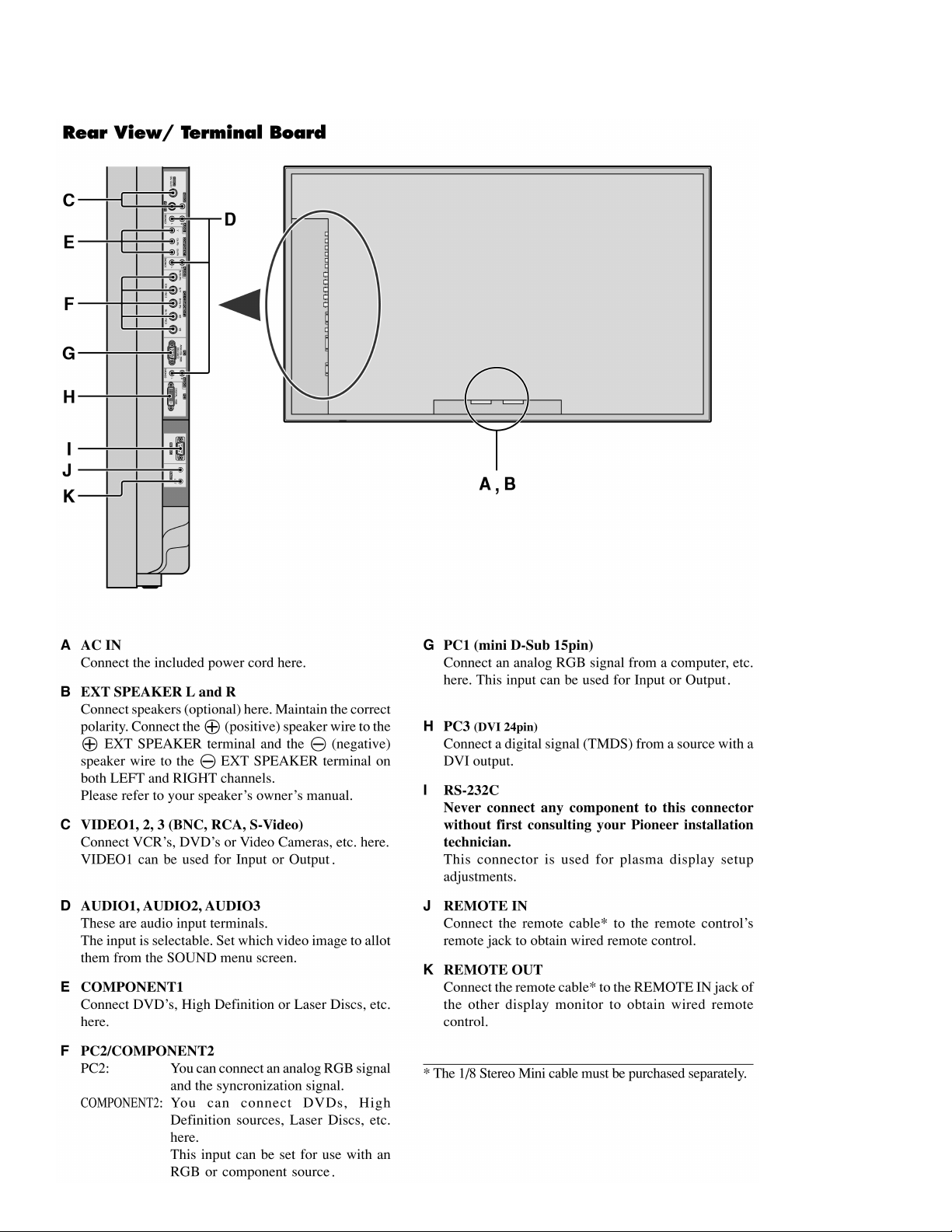
CONNECTION DIAGRAMS .................................................................. 13-1
CONNECTOR PIN EXPLANATION ...................................................... 14-1
BLOCK DIAGRAM ................................................................................ 15-1
1-1
Page 3

SAFETY INFORMATION
This service manual is intended for qualified service technicians ; it is not meant for the casual
do-it-yourselfer. Qualified technicians have the necessary test equipment and tools, and have been
trained to properly and safely repair complex products such as those covered by this manual.
Improperly performed repairs can adversely affect the safety and reliability of the product and may
void the warranty. If you are not qualified to perform the repair of this product properly and safely,
you should not risk trying to do so and refer the repair to a qualified service technician.
WARNING
This product contains lead in solder and certain electrical parts contain chemicals which are known to the state of California to
cause cancer, birth defects or other reproductive harm.
Health & Safety Code Section 25249.6 - Proposition 65
NOTICE
(FOR CANADIAN MODEL ONLY)
Fuse symbols (fast operating fuse) and/or (slow operating fuse) on PCB indicate that replacement parts
must be of identical designation.
REMARQUE
(POUR MODÈLE CANADIEN SEULEMENT)
Les symboles de fusible (fusible de type rapide) et/ou (fusible de type lent) sur CCI indiquent que les pièces
de remplacement doivent avoir la même désignation.
SAFETY PRECAUTIONS
NOTICE : Comply with all cautions and safety related notes
located on or inside the cabinet and on the chassis.
The following precautions should be observed :
1. When service is required, even though the PDP UNIT an
isolation transformer should be inserted between the power line
and the set in safety before any service is performed.
2. When replacing a chassis in the set, all the protective devices
must be put back in place, such as barriers, nonmetallic knobs,
adjustment and compartment covershields, isolation resistorcapacitor, etc.
3. When service is required, observe the original lead dress. Extra
precaution should be taken to assure correct lead dress in the
high voltage circuitry area.
4. Always use the manufacture's replacement components.
Especially critical components as indicated on the circuit
diagram should not be replaced by other manufacture's.
Furthermore where a short circuit has occurred, replace those
components that indicate evidence of overheating.
5. Before returning a serviced set to the customer, the service
technician must thoroughly test the unit to be certain that it is
completely safe to operate without danger of electrical shock,
and be sure that no protective device built into the set by the
manufacture has become defective, or inadvertently defeated
during servicing. Therefore, the following checks should be
performed for the continued protection of the customer and
servicetechnician.
6. Perform the following precautions against unwanted radiation
and rise in internal temperature.
• Always return the internal wiring to the original styling.
• Attach parts (Gascket, Ferrite Core, Ground, Rear Cover,
Shield Case etc.) surely after disassembly.
7. Perform the following precautions for the PDP panel.
• When the front case is removed, make sure nothing hits the
panel face, panel corner, and panel edge (so that the glass does
not break).
• Make sure that the panel vent does not break. (Check that the
cover is attached.)
• Handle the FPC connected to the panel carefully.
Twisting or pulling the FPC when connecting it to the
connector will cause it to peel off from the panel.
8. Pay attention to the following.
• When the front case is removed, infrared ray is radiated and
may disturb reception of the remote control unit.
• Pay extreme caution when the front case and rear panel are
removed because this may cause a high risk of disturbance to
TVs and radios in the surrounding.
2-1
Page 4
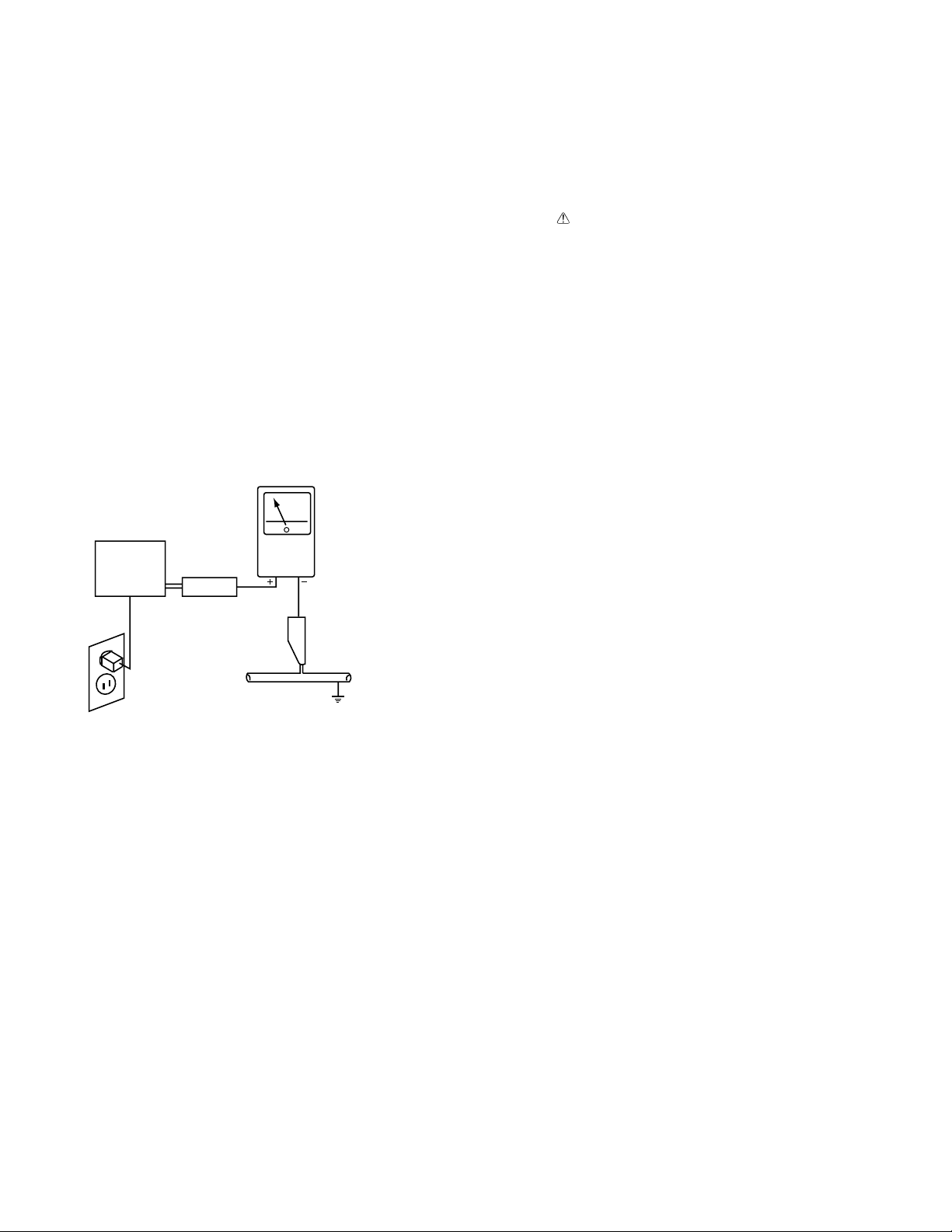
Leakage Current Cold Check
With the AC plug removed from an AC power source, place a
jumper across the two plug prongs. Turn the AC power switch on.
Using an insulation tester (DC 500V), connect one lead to the
jumpered AC plug and touch the other lead to each exposed metal
part (input/output terminals, screwheads, metal overlays, control
shafts, etc.), particularly any exposed metal part having a return
path to the chassis. Exposed metal parts having a return path to
the chassis should have a minimum resistor reading of 0.3MΩ
and a maximum resistor reading of 5MΩ. Any resistor value
below or above this range indicates an abnormality which
requires corrective action. Exposed metal parts not having a
return path to the chassis will indicate an open circuit.
Leakage Current Hot Check
Plug the AC line cord directly into an AC power source (do not
use an isolation transformer for this check).
Turn the AC power switch on.
Using a "Leakage Current Tester (Simpson Model 229
equivalent)", measure for current from all exposed metal parts of
the cabinet (input/output terminals, screwheads, metal overlays,
control shaft, etc.), particularly any exposed metal part having a
return path to the chassis, to a known earth ground (water pipe,
conduit, etc.). Any current measured must not exceed 0.5mA.
PRODUCT SAFETY NOTICE
Many electrical and mechanical parts in PIONEER set have
special safety related characteristics. These are often not evident
from visual inspection nor the protection afforded by them
necessarily can be obtained by using replacement components
rated for higher voltage, wattage, etc. Replacement parts which
have these special safety characteristics are identified in this
Service Manual.
Electrical components having such features are identified by
marking with a on the schematics and on the parts list in this
Service Manual.
The use of a substitute replacement component which dose not
have the same safety characteristics as the PIONEER
recommended replacement one, shown in the parts list in this
Service Manual, may create shock, fire or other hazards.
Product Safety is continuously under review and new instructions
are issued from time to time. For the latest information, always
consult the current PIONEER Service Manual. A subscription to,
or additional copies of, PIONEER Service Manual may be
obtained at a nominal charge from PIONEER.
Reading should
not be above
0.5mA
Earth
ground
Device
under
test
Also test with
plug reversed
(Using AC adapter
plug as required)
Leakage
current
tester
Test all
exposed metal
surfaces
AC Leakage Test
ANY MEASUREMENTS NOT WITHIN THE LIMITS
OUTLINED ABOVE ARE INDICATIVE OF A POTENTIAL
SHOCK HAZARD AND MUST BE CORRECTED BEFORE
RETURNING THE SET TO THE CUSTOMER.
2-2
Page 5
2-3
Page 6
2-4
Page 7
[Important Check Points for Good Servicing]
In this manual, procedures that must be performed during repairs are marked with the below symbol.
Please be sure to confirm and follow these procedures.
1. Product safety
Please conform to product regulations (such as safety and radiation regulations), and maintain a safe servicing environment by
following the safety instructions described in this manual.
1 Use specified parts for repair.
Use genuine parts. Be sure to use important parts for safety.
2 Do not perform modifications without proper instructions.
Please follow the specified safety methods when modification(addition/change of parts) is required due to interferences such as
radio/TV interference and foreign noise.
3 Make sure the soldering of repaired locations is properly performed.
When you solder while repairing, please be sure that there are no cold solder and other debris.
Soldering should be finished with the proper quantity. (Refer to the example)
4 Make sure the screws are tightly fastened.
Please be sure that all screws are fastened, and that there are no loose screws.
5 Make sure each connectors are correctly inserted.
Please be sure that all connectors are inserted, and that there are no imperfect insertion.
6 Make sure the wiring cables are set to their original state.
Please replace the wiring and cables to the original state after repairs.
In addition, be sure that there are no pinched wires, etc.
7 Make sure screws and soldering scraps do not remain inside the product.
Please check that neither solder debris nor screws remain inside the product.
8 There should be no semi-broken wires, scratches, melting, etc. on the coating of the power cord.
Damaged power cords may lead to fire accidents, so please be sure that there are no damages.
If you find a damaged power cord, please exchange it with a suitable one.
9 There should be no spark traces or similar marks on the power plug.
When spark traces or similar marks are found on the power supply plug, please check the connection and advise on secure
connections and suitable usage. Please exchange the power cord if necessary.
0 Safe environment should be secured during servicing.
When you perform repairs, please pay attention to static electricity, furniture, household articles, etc. in order to prevent injuries.
Please pay attention to your surroundings and repair safely.
2. Adjustments
To keep the original performance of the products, optimum adjustments and confirmation of characteristics within specification.
Adjustments should be performed in accordance with the procedures/instructions described in this manual.
3. Lubricants, Glues, and Replacement parts
Use grease and adhesives that are equal to the specified substance.
Make sure the proper amount is applied.
4. Cleaning
For parts that require cleaning, such as optical pickups, tape deck heads, lenses and mirrors used in projection monitors, proper
cleaning should be performed to restore their performances.
5. Shipping mode and Shipping screws
To protect products from damages or failures during transit, the shipping mode should be set or the shipping screws should be
installed before shipment. Please be sure to follow this method especially if it is specified in this manual.
2-5
Page 8
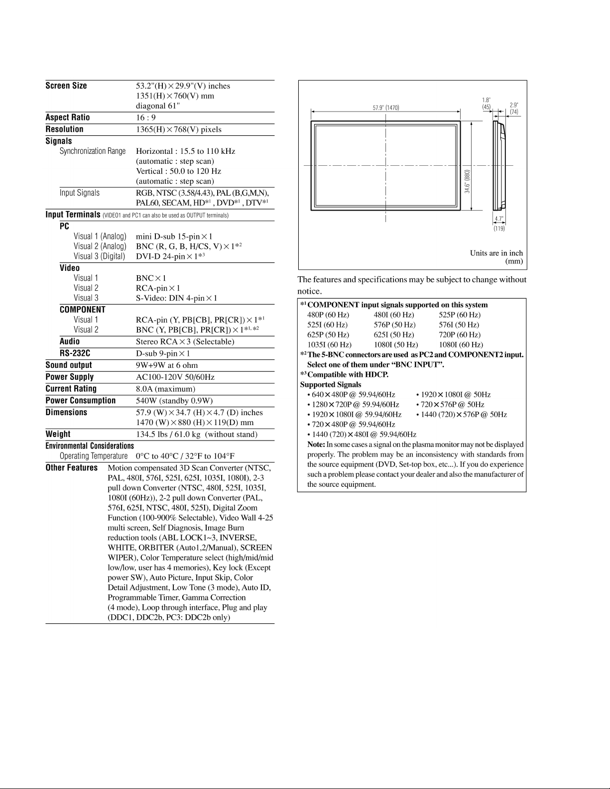
SPECIFICATIONS
PDP-614MX
3-1
Page 9
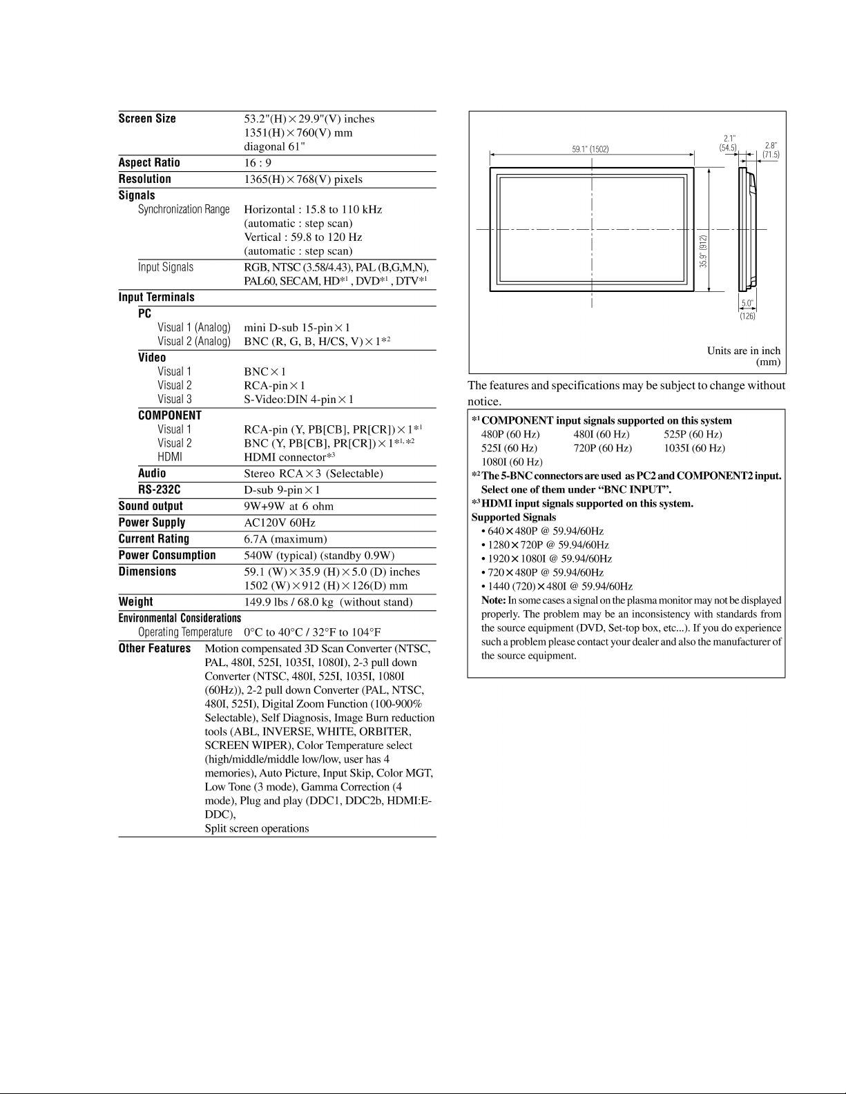
PRO-1410HD
3-2
Page 10
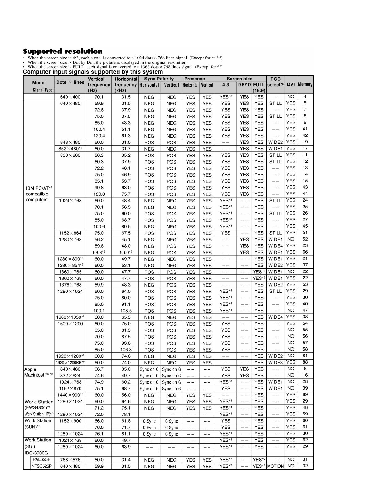
TABLE OF SIGNAL SUPPORTED
PDP-614MX
4-1
Page 11
4-2
Page 12
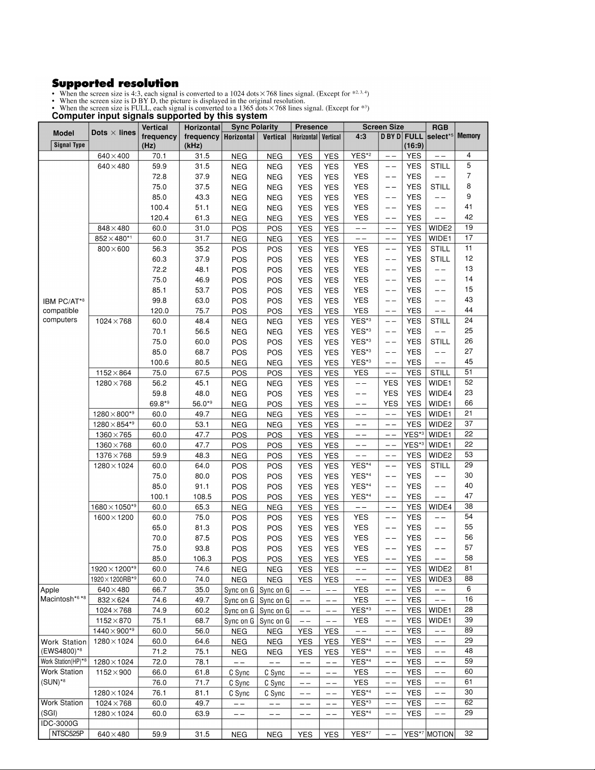
PRO-1410HD
4-3
Page 13
4-4
Page 14
PANEL FACILITIES
PDP-614MX
5-1
Page 15
5-2
Page 16
PRO-1410HD
5-3
Page 17
5-4
Page 18
CONTRAST OF MISCELLANEOUS PARTS
NOTES:
Parts marked by "NSP" are generally unavailable because they are not in our Master Spare Parts List.
The mark found on some component parts indicates the importance of the safety factor of the part.
Therefore, when replacing, be sure to use parts of identical designation.
Screws adjacent to mark on product are used for disassembly.
For the applying amount of lubricants or glue, follow the instructions in this manual.
(In the case of no amount instructions, apply as you think it appropriate.)
7 CONTRAST TABLE for PDP-614MX
PDP-614MX/LUC and PX-61XM3A are constructed the same except for the following:
Symbol
A01 MAIN1 PWB ASSY 937G3M01 937J8M01
A02 232C PWB ASSY 937F7SA1 937J8SA1
A03 CTL PWB ASSY 937F7SB1 937J8SB1
A04 PWR PWB ASSY 937F7SC1 937J8SC1
A05 LED PWB ASSY 937F7SD1 937J8SD1
A06 SENB PWB ASSY 937F7SE1 937J8SE1
A07 SENC PWB ASSY 937F7SF1 937J8SF1
A08 SEND PWB ASSY 937F7SG1 937J8SG1
A09 AUDIO PWB ASSY 937F7SH1 937J8SH1
A10 CCD PWB ASSY 937F6C01 Not used
CN-PI CN 2-WP(PI) 360W, 1672-18 7SWXV002 Not used
Mark
Symbol and Description
PX-61XM3A PDP-614MX/LUC
PWB ASSYS
MISCELLANEOUS ELECTRICAL PARTS
Part No.
Remarks
SRW18 PL-CPIMS*3*10*15KFE Not used 29N01431
M11 GASKET(L30*10*T10) Not used 29C01761
M12 GASKET(L50*10*T10) Not used 29C01771
M13 GASKET(L120*10*T10) Not used 29C01781
M14 GASKET(L30*6*T3) Not used 29C01791
M15 GASKET(L140*13*T1.5) Not used 29C01801
M16 FRONT PANEL(61XM2) 29D00612 Not used
M16 FRONT FRAME ASSY(614MX) Not used 29DS0591
M24 COVER CTL 29F00781 Not used
M24 COVER CTL-G Not used 29F01121
M26 CONTROL BUTTON 29G00311 Not used
M26 CONTROL BUTTON-G Not used 29G00401
M50 INDICATOR(50XM3) 29K00421 Not used
M52 TERMINAL SHEET M(50XM3)W 29K00571 Not used
M52 TERMINAL SHEET M(614MX) Not used 29K00711
M53 TERMINAL SHEET S(50XM3)W 29K00581 Not used
M53 TERMINAL SHEET S(614MX) Not used 29K00721
M54 FILTER(61A) 29KS0211 Not used
M54 FILTER(61B) Not used 29KS0171
M57 NSP NAME PLATE(61XM3A) 29L05811 Not used
M57 NSP NAME PLATE(PDP-614MX) Not used 29L06201
M62 SHILDING TAPE AL(25*50M) 29C01911 Not used
MECHANISM PARTS
6-1
Page 19
Symbol
Mark
Symbol and Description
Part No.
PX-61XM3A PDP-614MX/LUC
Remarks
SHT001 INFORMATION 61XM3A 7S801371 Not used
SHT002 OPERATION 50XM4A/61XM3A 7S801381 Not used
SHT002 INSTRUCTIONS(PDP-614MX) Not used 7S801711
SHT003 NOTICE SHEET US(PDP) 78038622 Not used
PK14 CARTON BOX(61XM3) 29MS3091 Not used
PK14 CARTON BOX T(PDP-614MX) Not used 29M01051
PK16 REM-T HAND UNIT RP-114 3S120221 Not used
PK16 REM-T HAND UNIT AXD1498 Not used 3S120241
PK31 NSP MODEL NAME LABEL 29L05951 Not used
PK33 POWER CORD CASE Not used 29MS3241
PRINTED & PACKING MATERIALS
6-2
Page 20
7 CONTRAST TABLE for PRO-1410HD
PRO-1410HD/LUC and PX-61XM3A are constructed the same except for the following:
Symbol
A01 MAIN1 PWB ASSY 937G3M01 937J9M01
A02 232C PWB ASSY 937F7SA1 937J9SA1
A03 CTL PWB ASSY 937F7SB1 937J9SB1
A04 PWR PWB ASSY 937F7SC1 937J9SC1
A05 LED PWB ASSY 937F7SD1 937J9SD1
A06 SENB PWB ASSY 937F7SE1 937J9SE1
A07 SENC PWB ASSY 937F7SF1 937J9SF1
A08 SEND PWB ASSY 937F7SG1 937J9SG1
A09 AUDIO PWB ASSY 937F7SH1 937J9SH1
A10 CCD PWB ASSY 937F7SH1 Not used
CN-PI CN 2-WP(PI) 360W, 1672-18 7SWXV002 Not used
SRW18 PL-CPIMS*3*10*15KFE Not used 29N01431
SRW38 PL-CPIMS*4*16*3KF Not used 910E4066
SRW39 PL-CPIMS*4*16*3KF Not used 910E4066
SRW40 PL-CPIMS*4*16*3KF Not used 910E4066
SRW41 CBIPS*4*12*15KFE Not used 29N01401
SRW42 CBIPS*4*12*15KFE Not used 29N01401
SRW43 CBIPS*4*12*15KFE Not used 29N01401
SRW44 CPIMS*4*8*3KF Not used 29N01521
SRW45 CBIPS*4*12*15KFE Not used 29N01401
M11 GASKET(L30*10*T10) Not used 29C01761
Mark
Symbol and Description
PX-61XM3A PRO-1410HD/LUC
PWB ASSYS
MISCELLANEOUS ELECTRICAL PARTS
MECHANISM PARTS
Part No.
Remarks
M12 GASKET(L50*10*T10) Not used 29C01771
M13 GASKET(L120*10*T10) Not used 29C01781
M14 GASKET(L30*6*T3) Not used 29C01791
M15 GASKET(L140*13*T1.5) Not used 29C01801
M16 FRONT PANEL(61XM2) 29D00612 Not used
M28 TERMINAL PANEL M(50XM3) 29H02551 Not used
M28 TERMINAL PANEL M(50XR4) Not used 29H03491
M50 INDICATOR(50XM3) 29K00421 Not used
M52 TERMINAL SHEET M(50XM3)W 29K00571 Not used
M52 TERMINAL SHEET M(ELITE) Not used 29K00731
M53 TERMINAL SHEET S(50XM3)W 29K00581 Not used
M53 TERMINAL SHEET S(ELITE) Not used 29K00741
M54 FILTER(61A) 29KS0211 Not used
M54 FILTER(61B) Not used 29KS0171
M57 NSP NAME PLATE(61XM3A) 29L05811 Not used
M57 NSP NAME PLATE(PRO-1410HD) Not used 29L06221
M62 SHILDING TAPE AL(25*50M) 29C01911 Not used
M73 CORNER PIECE OUT Not used 29H03651
M74 CORNER PIECE IN Not used 29H03661
M75 LED LENS-E Not used 29K00761
M76 IR CAP Not used 29K00771
M77 ELITE BADGE Not used 29K00811
M78 OVER BEZEL TOP Not used 29P01501
M79 OVER BEZEL SIDE Not used 29P01511
M80 OVER BEZEL BOTTOM Not used 29P01521
M81 CORNER BRACKET Not used 29P01541
M82 CORNER PLATE SASSY-1 Not used 29PS0911
M83 CORNER PLATE SASSY-2 Not used 29PS0921
M84 SIDE PLATE SASSY Not used 29PS0931
M85 SHIELDING TAPE 25X25 Not used 29J01361
6-3
Page 21
Symbol
Mark
Symbol and Description
Part No.
PX-61XM3A PRO-1410HD/LUC
Remarks
SHT001 INFORMATION 61XM3A 7S801371 Not used
SHT002 OPERATION 50XM4A/61XM3A 7S801381 Not used
SHT002 INSTRUCTIONS PRO-1410HD Not used 7S801721
SHT003 NOTICE SHEET US(PDP) 78038622 Not used
PK05 CUSHION(TL) 29MS2611 Not used
PK05 CUSHION(TL)E Not used 29MS3161
PK06 CUSHION(TC) 29MS2621 Not used
PK06 CUSHION(TC)E Not used 29MS3171
PK07 CUSHION(TR) 29MS2631 Not used
PK07 CUSHION(TR)E Not used 29MS3181
PK08 CUSHION(BL) 29MS2641 Not used
PK08 CUSHION(BL)E Not used 29MS3191
PK09 CUSHION(BC) 29MS2651 Not used
PK09 CUSHION(BC)E Not used 29MS3201
PK10 CUSHION(BR) 29MS2661 Not used
PK10 CUSHION(BR)E Not used 29MS3211
PK11 CUSHION(BTM-L) 29MS2671 Not used
PK11 CUSHION(BTM-L)E Not used 29MS3221
PK12 CUSHION(BTM-R) 29MS2681 Not used
PK12 CUSHION(BTM-R)E Not used 29MS3231
PK14 CARTON BOX(61XM3) 29MS3091 Not used
PK14 CARTON BOX T(PRO-1410HD) Not used 29M01071
PK16 REM-T HAND UNIT RP-114 3S120221 Not used
PK16 REM-T HAND UNIT AXD1499 Not used 3S120251
PK17 BAG,POLYETHYLENE(150*370) 24813191 Not used
PRINTED & PACKING MATERIALS
PK28 BAG,POLYETHYLENE(150*370) Not used 24813191
PK31 NSP MODEL NAME LABEL 29L05951 Not used
PK33 POWER CORD CASE Not used 29MS3241
6-4
Page 22

HOW TO DIAGNOSE THE PDP MODULE
(PDP-NP61C2MF01)
1. List of tools required for repair
2. Points of failure diagnosis for a Board Assy (PKG)
3. Replacement method of a Board Assy (PKG)
and notes on replacement
4. Adjustments after replacement of parts in the module
5. Operation check
1. List of tools required for repair
a) Phillips screwdriver:For detaching/reattaching PKGs
b) Antistatic wrist strap:
To be used when electronic components, such as PKGs, are to be handled
c) Signal generator (PC, etc.) :For voltage adjustment and display check
d) Powe:For voltage adjustment and display check
f)Tester:For cable check, voltage adjustment, etc.
g) Cushion:To be used when the PKGs are to be replaced
Note: Be sure to wear a wrist strap when you detach/reattach PKGs (Board Assy) to protect
electronic components from being damaged by electrostatic charges.
7-1
Page 23
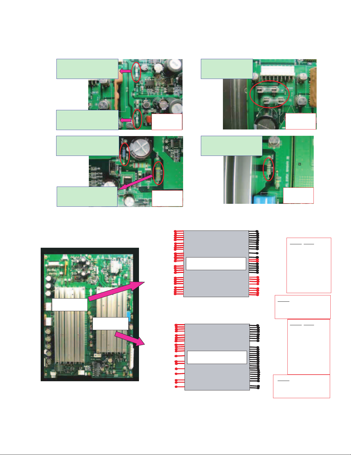
2. Points of failure diagnosis for a Board Assy (PKG)
The fuses and/or fusible resistors shown in the photos below may be blown by electric
surges caused by a failure. In such a case, replace the corresponding PKG.
Failure diagnosis of the Scanning PKG
Fusible resistor (R12) located
at the upper-left corner of the
Scanning PKG: Approx. 1.0 Ω
(1/2 W)
Fusible resistor (R29) located
at the upper-left corner of the
Scanning PKG: Approx. 4.7 Ω
(1/4 W)
OK: Short-
circuited,
NG: Open
Glass fuses (F1 and F2)
located at the upper-left
corner of the Scanning
PKG
OK: Short-
circuited,
NG: Open
Fusible resistor (R108A)
located at the lower-right corner
of the Scanning PKG: Approx.
2.2 Ω (1 W)
Fusible resistor (R113) located
at the lower-right corner of the
Scanning PKG: Aapprox. 4.7 Ω
(2 W)
OK: Short-
circuited,
NG: Open
Fusible resistor (R111) located
at right center of the Scanning
PKG: Approx. 10 Ω (1 W)
Failure diagnosis of the Power HIC on the Scanning PKG
D
(58~62)
E
(53~56)
F
(47~51)
G
(42~45)
H
(37~40)
I
(32~35)
PH2311(rear view)
PH2311
Note: A, D, and E are ground.
11
1
13
A
20
B
C
9
(14~15)
(23~26)
(28~31)
Result:
OK: k Ω or more,
NG: Short-circuited
OK: Short-
circuited,
NG: Open
Check points
Between A and B
Between B and H
Between C and I
Between D and E
Between F and G
PH2312
A
(59~62)
B
(54~57)
52
49
C
E
G
I
(42)
(38)
(34)
(46)
D
(43)
F
(40)
H
(35)
J
(32)
PH2312(rear view)
Note: C and G are ground.
7-2
1
8
11
27
30
31
Check points
Between A and B
Between C and D
Between E and F
Between G and H
Between I and J
Result:
OK: k Ω or more,
NG: Short-circuited
Page 24
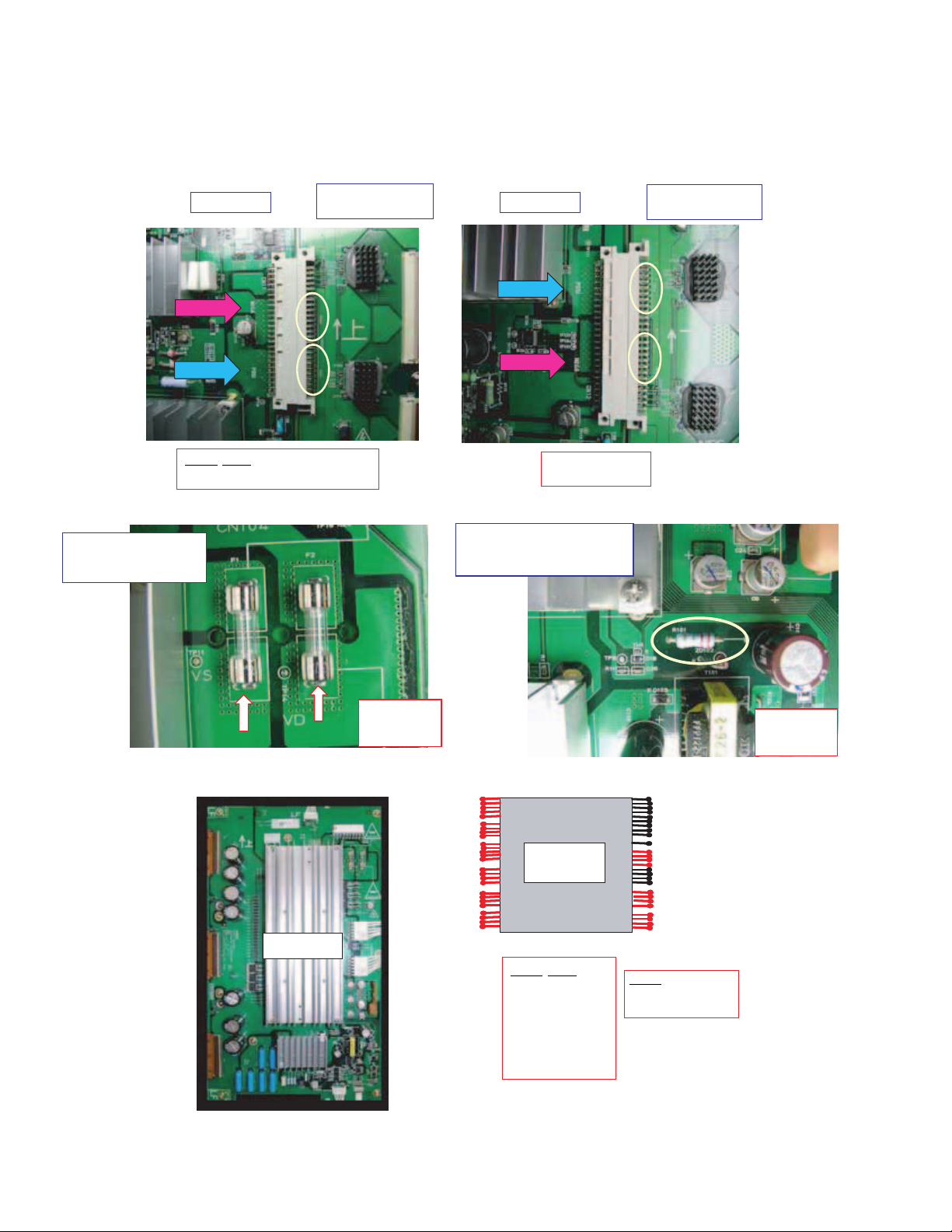
Failure diagnosis of the Scanning IC
Check with a tester the resistance value between any pins indicated as NEGA and POSI of the
connector in the photos below. If a positive and a negative pin of the connector on the Scanning
Relay PKGs are short-circuited and remains short-circuited even after the connectors on the
Scanning PKG and Scanning Relay PKG are disconnected, the Scanning IC on the Scanning Relay
PKG is in failure.
Scanning PKG Scanning PKG
NEGA
NEGA
POSI
POSI
Check points
Between any pins of
NEGA and POSI blocks
Scanning Relay PKG
(upper connector)
Failure diagnosis of the Common PKG
Glass fuses (F1 and F2) at
the upper-right corner of
the Common PKG
POSI
POSI
NEGA
NEGA
OK: k Ω or more,
NG: Short-circuited
Fusible resistor (R101) at the
lower-right corner of the Common
PKG: Approx. 2.2 Ω (1 W)
Scanning Relay PKG
(lower connector)
OK: Short-
circuited,
NG: Open
Failure diagnosis of the Power HIC on the Common PKG
D
(58~62)
E
(53~56)
F
(47~51)
G
(42~45)
H
(37~40)
I
(32~35)
PH2311
Check points
Between A and B
Between B and H
Between C and I
Between D and E
Between F and G
Note: A and D are ground.
PH2311
(rear view)
1
9
11
A
(13~16)
20
B
(23~26)
C
(28~31)
Result:
OK: k Ω or more,
NG: Short-circuited
OK: Short-
circuited,
NG: Open
7-3
Page 25
Failure diagnosis of the Data HIC
Failure symptom: The image in any block of the screen is not displayed.
Check with a tester between Pin 5 or 6 (Vd line of Data IC)
and ground of each Signal Relay PKG.
OK: Open
NG: Short-
circuited,
CN2
CN8CN8CN2
CN8
CN3
CN8
CN3
Failure diagnosis of the Digital PKG
Chip fuse (FU701) at the
upper-right corner of the digital
PKG
CN8
7-4
OK: Short circuited,
NG: Open
Page 26
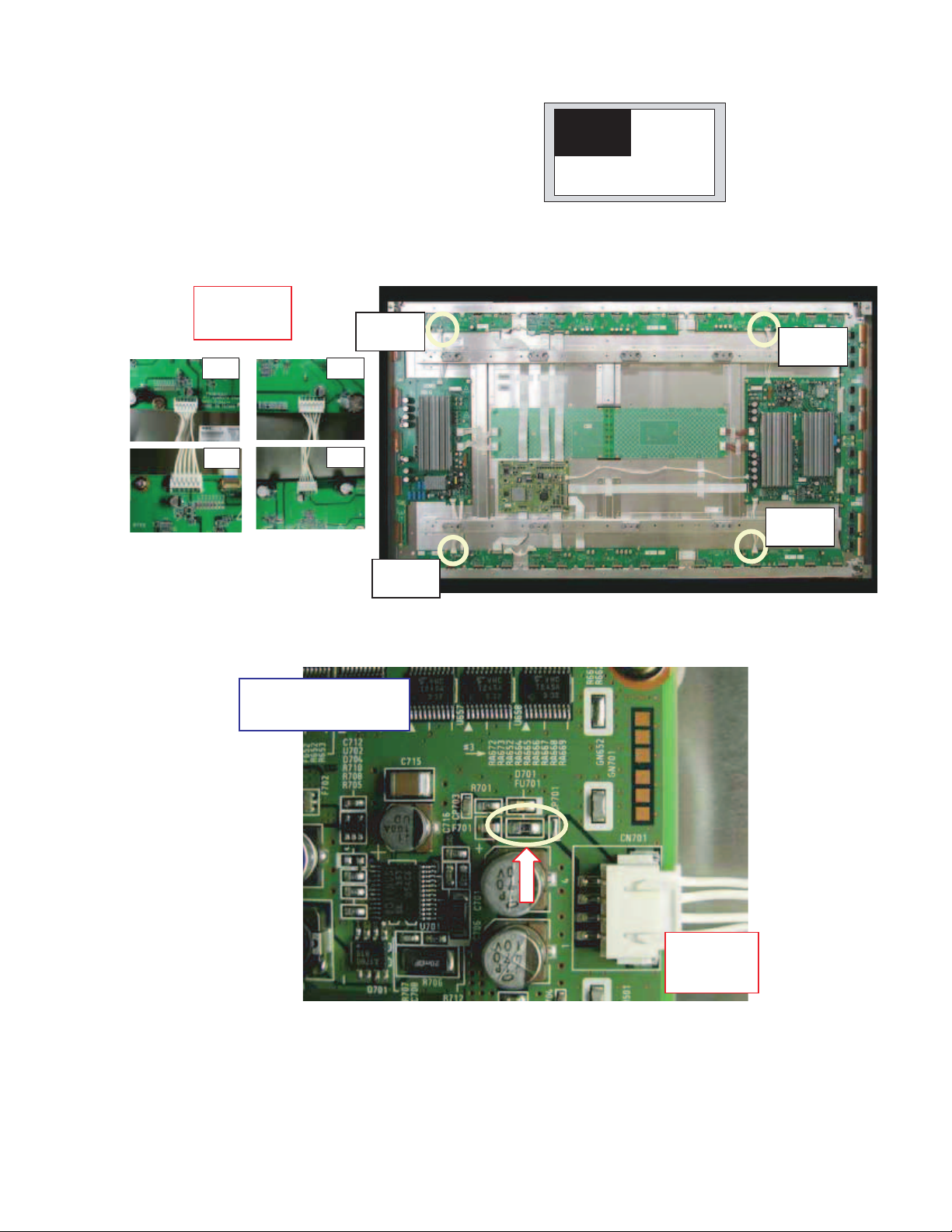
3. Replacement method for a Board Assy (PKG) and notes on replacement
Preparation
Place a cushion on the workbench and set the module to be repaired on it.
Note: With the glass surface facing downward, be sure that the entire glass surface is
against the cushion.
Disconnection of connectors and cables
Disconnect all the connectors on the PKG to be repaired.
(When a Signal Relay PKG is to be removed, remove the heat sink beforehand.)
Common Branch
PKG (upper): One
connector
Common Branch
PKG (lower): One
connector
Flat cable
(longitudinal type)
Signal Relay PKG (upper
left): 7 connectors
Common board:
10 connectors
Digital PKG: 8
connectors
Signal Relay PKG (lower
left): 8 connectors
Flat cable
Lock. Lock. Lock. Lock.
(horizontal type 1)
Signal Relay PKG (upper
center): 10 connectors
Recovery Relay PKG
Signal Relay PKG (lower
center): 10 connectors
Flat cable
(horizontal type 2)
Signal Relay PKG
(upper right): 8 connectors
Scanning PKG:
8 connectors
Signal Relay PKG
(lower right): 8 connectors
Cable type
Scanning Relay PKG
(upper): 5 connectors
Scanning Relay PKG
(lower): 5 connectors
Unlock. Unlock. Unlock. Unlock.
7-5
Page 27
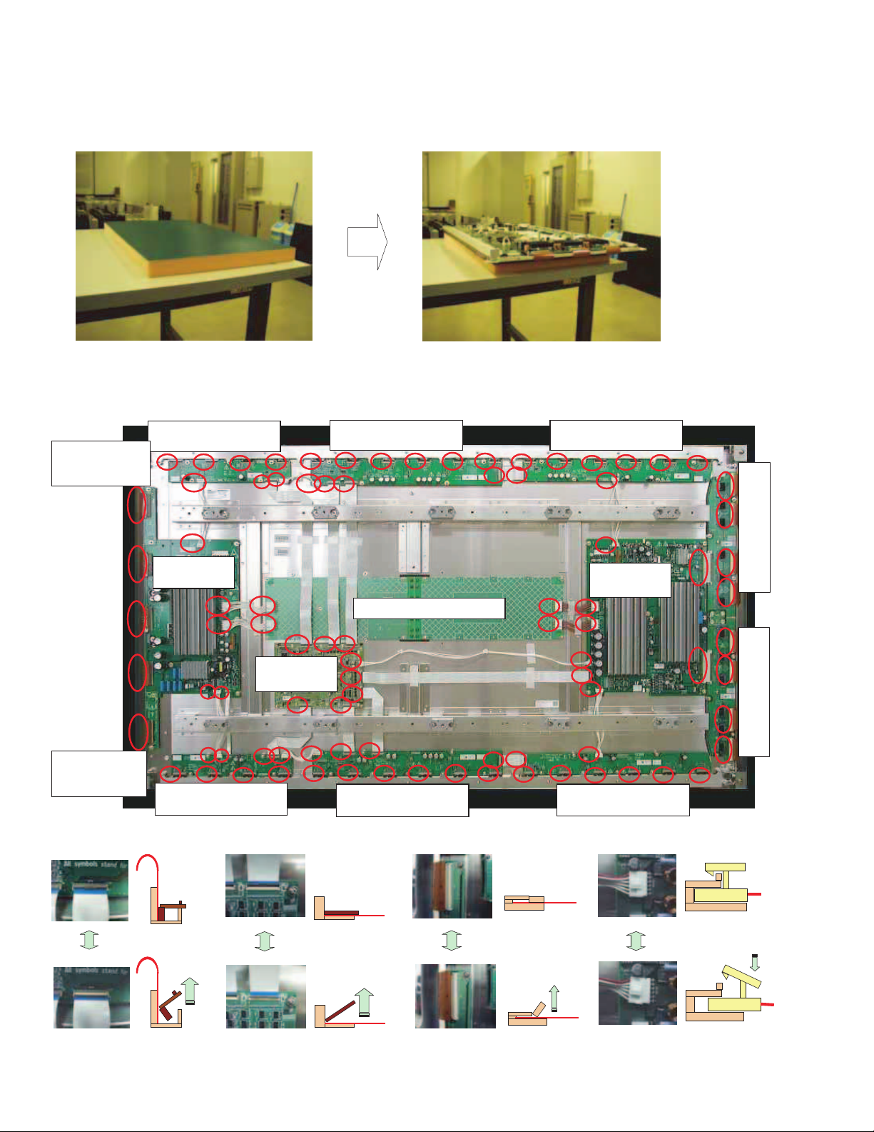
How to remove/reattach the Board Assy (PKGs)
Notes: · Be sure not to drop a screwdriver or screw on a PKG or a cable.
· When removing/reattaching a screw, be sure not to leave any tiny metal shavings, because
they may cause a failure.
· Before removing Signal Relay PKGs, remove the heat sink.
· Be sure not to apply any stress to a PKG, connector, or cable when reattaching them.
· Reattach Signal Relay PKGs before reattaching the heat sink.
Heat sink: 17 screws
Common Branch PKG
(upper): One screw
Common PKG: 8 screws
Common Branch PKG
(lower): One screw
Signal Relay PKG
(upper left): 4 screws
Digital PKG:
4 screws
Signal Relay PKG
(lower left): 4 screws
Signal Relay PKG (upper
center): 5 screws
Recovery Relay PKG :11screws
Signal Relay PKG
(lower center): 5 screws
Signal Relay PKG (upper
right): 5 screws
Scanning PKG: 9 screws
Signal Relay PKG
(lower right): 5 screws
Confirmation of connector connection
Check whether or not the connectors indicated by circles are correctly connected.
Scanning Relay PKG
(upper): 6 screws
Scanning Relay PKG
(lower): 5 screws
Heat sink: 17 screws
Signal Relay PKG
(upper left): 7 connectors
Common board:
10 connectors
Digital PKG:
8 connectors
Signal Relay PKG (lower
left): 8 connectors
Signal Relay PKG (upper
center): 10 connectors
Common branch PKG
Signal Relay PKG (lower
center): 10 connectors
Signal Relay PKG (upper
right): 8 connectors
Scanning PKG:
8 connectors
Signal Relay PKG (lower
right): 8 connectors
Scanning Relay PKG
(upper): 5 connectors
Scanning Relay PKG
(lower): 5 connectors
7-6
Page 28
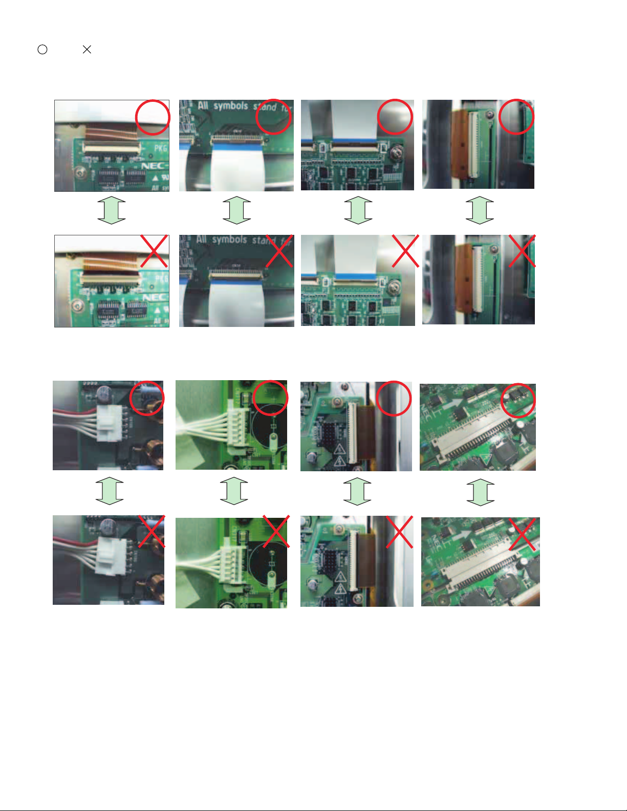
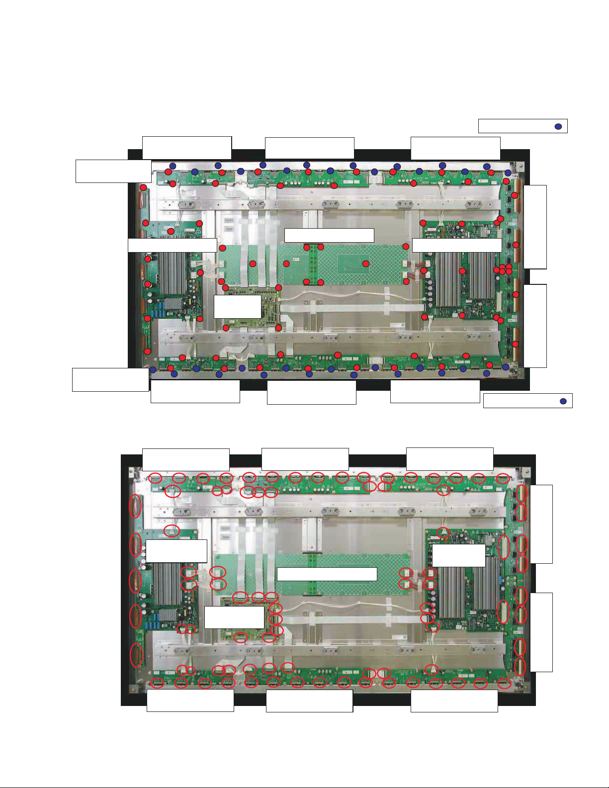
Confirmation of connector connection and locking statuses
: OK : NG
Between the Data IC and Signal
Relay PKG (photo)
Between the Scanning PKG
(photo) and Recovery Relay PKG
Between the Signal Relay PKG
(photo) and Digital PKG
Between the Signal Relay PKG
and Scanning PKG (photo)
Between the Signal Relay PKG
and Digital PKG (photo)
Between the Scanning Relay PKG
(photo) and panel
Between the panel and
Common PKG (photo)
Between the Scanning PKG (photo)
and Signal Relay PKG (photo)
7-7
Page 29
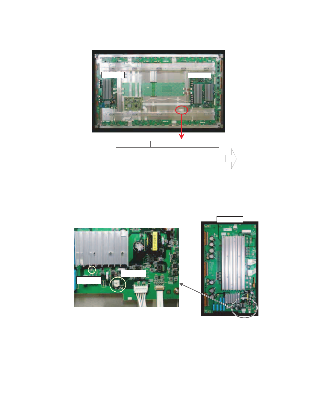
4. Adjustments after replacement of parts in the module
After the module has been reassembled, adjust the panel-drive voltages as indicated below:
Check Vbw, Vsw, and Vp voltages (values specific for each panel) indicated on the drivevoltage label.
Common PKG
Drive-voltage label
(s185.0 / d65.0)115.2/209.9/199.8
(s185.0 / d65.0)115.2/209.9/199.8
*************************************
*************************************
311200062
311200062
Vsw Vp
Vsw Vp
Vbw
Vbw
Scanning PKG
Example
V
bw : 115.2V
Vsw:209.9V
Vp : 199.8V
Vsw adjustment inside the Common PKG
Points to measure: Voltage between TP10 and GND (chassis GND) on the Common PKG
Adjustment method: Adjust VR101 so that the Vsw value of TP10 becomes in the range of
±0.5 V of the Vsw value indicated on the drive-voltage label.
Common PKG
TP10
VR101
7-8
Page 30
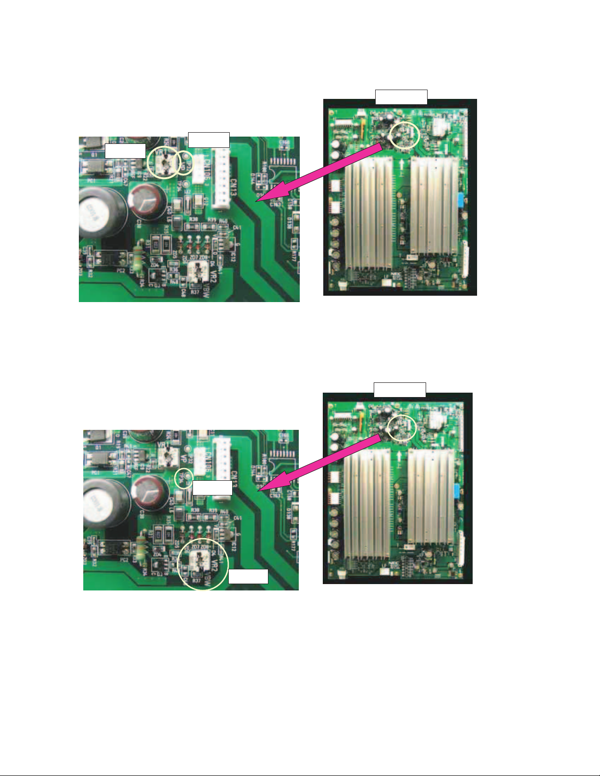
Vp adjustment inside the Scanning PKG
Points to measure: Voltage between TP32 and GND (chassis GND) on the Scanning PKG
Adjustment method: Adjust VR1 so that the Vp value of TP32 becomes in the range of ±1.5 V
of the Vp value indicated on the drive-voltage label.
Scanning PKG
TP32
VR1
Vbw adjustment inside the Scanning PKG
Points to measure: Voltage between TP34 and GND (chassis GND) on the Scanning PKG
Adjustment method: Adjust VR2 so that the Vbw value of TP34 becomes in the range of ±0.5
V of the Vbw value indicated on the drive-voltage label.
Scanning PKG
TP34
VR2
7-9
Page 31

5. Operation check
After replacing the module or parts inside the module, perform aging for 30 minutes or more
while displaying a fully white screen.
After that, check the screen by displaying a fully red, fully green, and fully blue screen, color
bars, and gray scale.
Note: If any flashing or luminescent spots are recognized during display check after a long period of
storage of the module, perform aging with a fully white screen displayed for another hour or so.
7-10
Page 32

7-11
Page 33

8-1
TROUBLESHOOTING
• Problems in the power supply, such as “Failure in Power ON” or “LED flashing or lighting (alarm
display)”
→ 1. Go to Power failure (P8-2).
• Problems in the images, such as “No pictures available”
→ 2. Go to Image errors (P8-8).
• No video loop-out signal is generated.
→ The MAIN PWB is faulty.
• “Remote control not effective”
→ 3. Go to Audio errors (P8-14).
• “Remote control not effective”
→ 4. Go to Remote control not effective (P8-15).
• The closed caption is displayed incorrectly. (PX-*****A only)
→ 5. Go to "The closed caption (CC) is displayed incorrectly." (P8-17).
Page 34

1. Power failure
(p
8-2
(1) The power supply is not turned on.
Move the main power setting for
OFF→ ON.
Is the POWER/STANDBY lamp lit?
(2) Blinking in green (Alarm of
temperature sensor error or fan error)
Go to (P8-3)
(3) Blinking in red after repeating
reciprocal flash in red and green
(POWER ON↔OFF) 3times (Alarm of
temperature error) Go to (P8-5).
(4) Reciprocal flashing in red and
green (Alarm of panel error) Go to
(P8-6).
(5) Lighting in green, and then in
red (Alarm of power line error) Go to
(P8-7).
Is a 5Vdc output available in the state that
the LD connector is disconnected and the
main power is turned ON?
YES
NO
Is a 5Vdc output available in the state that
the RS connector is disconnected and the
main power is turned ON?
YES
NO
The PW connector, PWR PWB or the MAIN
PWB is fault.
YES
The LD connector or the
LED PWB is fault.
The RS connector or the
232C PWB is fault.
(Caution) If any abnormality is sensed in such a
NO
Is the AC power
output available at
the AC connector
ower cord)?
YES
Is a 6.8Vdc output
available at Pin of
the PM connector?
YES
Is a 6.8Vdc output
available at Pin of
the PW connector?
YES
Is a 6.8Vdc output
available at Pin of
the PM connector?
YES
Is a 4.9Vdc output
available at Pin of
the PM connector?
NO
Is a 5Vdc output
available at Pin of
the PW connector?
NO NO NO
The MAIN PWB is fault.
manner that the LED flashes or lights, all
the power lines other than those of 7Vdc
(M+7V) and 5Vdc (M+5V) are automatically
turned off in about 10 seconds. When
checking the power lines other than those of
M+7V and M+5V, a circuit tester or the like
should have been connected in advance.
NO
The PW
connector or
the PWR PWB
is fault.
NO
The PM
connector or
the MAIN
PWB is fault.
NO
NO
The power cord is defective.
Is a 6.8Vdc output available in
the state that the LD connector
is disconnected and the main
power is turned ON?
The LD
YES
connector or
the LED PWB
NO
Is a 6.8Vdc output available in
the state that the PW connector
is disconnected and the main
power is turned ON?
NO
Is a 6.8Vdc output available in
the state that the PM connector
is disconnected and the main
power is turned ON?
is fault.
The PW
YES
connector or
the PWR PWB
is fault.
YES
The PM
connector or
the MAIN
PWB is fault.
NO
YES
The power unit is fault.
YES
Page 35

(2) Blinking in green
8-3
Alarm of te mperature sensor error
Blinking in green (intervals of 2 seconds)
Turn off the main power supply.
Pressing the [MENU] key of the product,
turn on the main power supply to cancel
alarming.
Press the remove control keys in the
sequential order of [POWER ON] →
[POWER ON] → [EXIT] → [DISPLAY] and
enter the factory adjustment menu. Press
the [MENU/ENTER] key to
display the FAN SET menu (P2/11).
Is there a display of
numerals (almost room
temperatures) at the right
side of [T1, T2, T3]?
YES
The MAIN PWB is fault.
NO
FAN SET
FAN SET
FAN MODE H CONT ENA –
FAN OFF/L – CONT UP –
FAN L/M – CONT TIME –
FAN M/H – UP STEP 2
SF SAVE 075 DOWN STEP 2
PLE SAVE 070 READ TIME 60
T ALM 095 TEMP LEVEL 1
RET TME 030
PLE TIME 001
T1 030 T2 025
T3 030 T4 – MODE 2
IC ERROR –
[MENU/ENTER] NEXT [EXIT] PREV 2/11
Is there a display of [-] for
all the numerals at the
right side of [T1, T2, T3]?
YES
Are there a 3.3Vdc
output at Pin and a
clock signal (3.3Vpp)
at Pins and of the
TS in the state that the
TS connector is
disconnected and the
NO
NO
main power supply is
turned on?
The TS connector
YES
or the SENC PWB
is fault.
When a [-] display is presented, the PWB with the symbol shown
below is fault. T1: SEND PWB, T2: SENB PWB, T3: SENC PWB
Are there a 3.3Vdc
output at Pin and a
clock signal (3.3Vpp)
at Pins and of the
TR in the state that the
TR connector is
disconnected and the
main power supply is
turned on?
YES
The TR connector
or the SEND PWB
is fault.
Are there a 3.3Vdc
output at Pin and a
NO
clock signal (3.3Vpp)
at Pins and of
the TM in the state
that the TM connector
is disconnected and
the main power
supply is turned on?
YES
The TM connector
or the SENB PWB
is fault.
NO
The MAIN PWB
is fault.
Page 36

Alarm of fan error
8-4
Blinking in green (intervals of
0.5seconds)
Turn off the main power supply.
Pressing the [MENU] key
of the product, turn on the
main power supply to
cancel alarming.
Is the fan running?
(Caution) When alarming is
canceled, [FAN MODE] of
FAN SET (P2/11) in the
factory adjustment menu
automatically moves from
[ENA] to [H], thus causing
the fan to run.
FAN SET
FAN MODE ENA CONT ENA –
FAN OFF/L – CONT UP –
FAN L/M – CONT TIME –
FAN M/H – UP STEP 2
FAN SAVE 075 DOWN STEP 2
PLE SAVE 070 READ TIME 60
T ALM 095 TEMP LEVEL 1
RET TME 030
PLE TIME 001
T1 030 T2 025
T3 030 T4 – MODE 2
IC ERROR –
[MENU/ENTER] NEXT [EXIT] PREV 2/11
FAN SET
FAN MODE H CONT ENA –
FAN OFF/L – CONT UP –
FAN L/M – CONT TIME –
FAN M/H – UP STEP 2
FAN SAVE 075 DOWN STEP 2
PLE SAVE 070 READ TIME 60
T ALM 095 TEMP LEVEL 1
RET TME 030
PLE TIME 001
T1 030 T2 025
T3 030 T4 – MODE 2
IC ERROR –
[MENU/ENTER] NEXT [EXIT] PREV 2/11
YES
NO
Is there a 3.3Vdc output
at Pin of the FA and
FB, FC connectors?
Is there a voltage output of 11.3Vdc for PX42XM3/XR3, 11.2Vdc for PX-50XM4/XR4, and
9.3Vdc for PX-61XM3/XR3, respectively, at Pin
1 of the FA, FB, and FC connectors?
NO
Is there a voltage output of
11.3Vdc for PX-42XM3/XR3,
11.2Vdc for PX-50XM4/XR4, and
9.3Vdc for PX-61XM3/XR3,
respectively, when the FA
connector is disconnected and the
mains power is turned ON?
YES
YES
NO
The FAN-A/FAN-B/FAN-C is fault.
Is there a voltage output of
11.3Vdc for PX-42XM3/XR3,
11.2Vdc for PX-50XM4/XR4, and
9.3Vdc for PX-61XM3/XR3,
respectively, when the FB
connector is disconnected and the
mains power is turned ON?
YES
The FAN-A is fault.
The FAN-B is fault.
YES
The fan is out of order on the
side where a 3.3Vdc output
is generated.
NO
The MAIN PWB is fault.
(Caution) The FAN-C and FC
Is there a voltage output of
11.3Vdc for PX-42XM3/XR3,
11.2Vdc for PX-50XM4/XR4, and
9.3Vdc for PX-61XM3/XR3,
respectively, when the FC
connector is disconnected and the
NO
mains power is turned ON?
NO
YES
The FAN-C is fault.
connectors are used
only for the 61XM3
Series.
The MAIN PWB
is fault.
(Caution) In the FAN MODE, [ENA] is automatically recovered when the main power is turned OFF → ON.
Page 37

(3) Blinking in red (Alarm of temperature error)
8-5
Since the internal temperature is too high in the product, the temperature protector has been actuated. In such
a case, the following actions should be taken immediately:
1. Turn off the main power supply and pull out the power cord from the wall outlet.
2. Wait for about 60 minutes until the temperature in the main unit lowers.
3. Check whether the heat discharge port is covered with dust or the like. If yes, remove the clogging substance.
4. If the unit is used where the ambient temperature is high, it should be moved to an adequate place (air
temperature ranging from 5°C to 35°C).
Page 38

(4) Alternation blinking in red and green (Alarm of PDP error)
8-6
(Caution) How to reset the alarming condition
Blinking in red and green
Move the main power
setting for OFF → ON.
Is there alternation blinking
in red and green?
Turn OFF the main power
supply.
With the [Menu] key of the
product kept pressed, turn
on the main power supply
to assume the [Voltage
Check Mode].
Pressing the [Input Select] key of the product, turn on the main power supply
of the main unit. In this state, keep pressing the [Input Select] key for more
than 2 seconds until alarming is canceled. Make confirmation by the method
specified below.
NO
Normal
YES
(Caution) When the main power supply is turned on with the
[Menu] key of the product kept pressed, it takes 30
seconds more to assume the state of [blinking in red and
green]. In this time period, the following voltage checks
should be carried out.
If the state of [blinking in red and green] is assumed
during this checking, take actions of [Alarm Canceling]
and [Voltage Check Mode Setup] again.
Is there a 3.3Vdc output at
Pin 94 of IC9501 in the
MAIN PWB? (See the
PWB Layout Diagram on
P4-20.)
Turn ON the main power
supply in the state that the
AD, PD, and PH connectors
are disconnected. In this
state, are there the outputs
of Vs (170Vdc), Vd (60Vdc),
and 5Vdc at the PD/PH
connectors as specified in
the table at right? In this
case, however, no images
are generate.
NO
YES
The PDP is fault.
YES
NO
The MAIN PWB is fault.
The Power unit is fault.
(Caution) The voltage values of Vd and Vs and also the connector
pin numbers can differ according to the PDP. The method
of checking these voltage values is obtainable from [2.
Adjustment of the power unit] in the method of adjustment
plus the table specified below.
Inch Vs Vd GND 5Vdc GND
42/50 PD-9pin PD-7pin PD-5pin PH-1pin PH-3pin
61
PD-9pin
PH-1pin
PD-7pin
PH-4pin
PD-5pin
PH-5pin
PD-4pin
PH-7pin
PD-5pin
PH-5pin
(Refer to P7-1 "HOW TO DIAGNOSE THE PDP MODULE".)
Page 39

(5) Lighting in green, and then in red (Alarm of power voltage error)
g
8-7
Unlike [lighting in red] in the STANDBY mode, [lighting in green] continues for about 30 seconds without any
output of images and audio signals. Since then, the mode turns into [lighting in red].
Lighting in red
Make an OFF → ON setting
twice for the main power
supply in order to reset the
alarming condition.
Is the LED lit in red after it
has been lit in green for about
30 seconds?
YES
When the main power supply is turned on in
the state that the AD, PD, and PH
connectors are disconnected, are there the
Vs (170Vdc) and Vd (60Vdc) outputs at Pins
- to Pins - of the PD connector and
a 5Vdc output at Pins - of the PH
connector? In this case, is the LED not
turned in red after it has been lit in green for
about 30 seconds? At that time, however, no
ima
es are generated.
NO
When the main power supply is turned on in
the state that the PA and PV connectors are
disconnected from one after another, is
there a 12Vdc output at Pins - of the PA
connector or the 12Vdc and 6Vdc outputs at
Pins and - of the PV connector? In
this case, is the LED not turned in red after it
has been lit in green for about 30 seconds?
NO
(Caution) How to reset the alarming condition The
alarming condition can be reset when an
OFF→ ON setting is repeated twice for the
main power supply in the state that the
LED is lit in red. The interval between the
first and second settings is not particularly
specified.
Normal
Refer to P7-1
"HOW TO DIAGNOSE THE PDP MODULE".
YES
YES
The PDP is fault.
(Caution) The voltage values of Vd and Vs
can differ according to the PDP.
The method of checking these
voltage values is obtainable from
[2. Adjustment of the power unit]
in the method of adjustment.
The MAIN PWB or the
AUDIO PWB is fault.
Is there an output of 3.3Vdc available at Pins
~ and 2.5Vdc at Pins ~ in the
state that the PA and PV connectors are
returned to the former state, the main power
is turned ON, and the PN connector is
disconnected? In this case, however, this
check must be finished in 30 seconds.
Otherwise, there will be power tripping on
account of an alarm.
NO
YES
The MAIN PWB is fault.
NO
The Power unit or the
PN connector is fault.
Page 40

8-8
2. Image errors
(Caution) Typical abnormal images are shown below. All errors do not always fall on these error samples.
(1) Image burn and deterioration in brigh
Residual images are seen
without signal entry.
(2) Failure in writing
(Refer to P7-1 "HOW TO DIAGNOSE THE PDP MODULE".)
This is not a fault.
Deterioration in brightness
This is not a fault.
Failure in writing
The PDP is fault.
tness
A
No signal
All-whitesignal
All-whitesignal
Dot errors change
with no continuity.
All-whitesignal
Page 41

(4) Wrong lighting
8-9
Wrong lighting
The PDP is fault.
(Refer to P7-1 "HOW TO DIAGNOSE THE PDP MODULE".)
All-black signal
Dot errors change
with no continuity.
All-black signal
(5) Dark images [Other than the deterioration in brightness as per (1) above]
The images are dark even
with an all-white input
The PDP is fault.
(Refer to P7-1 "HOW TO DIAGNOSE THE PDP MODULE".)
(6) Defect in horizontal lines
Line defect
The PDP is fault.
(Refer to P7-1 "HOW TO DIAGNOSE THE PDP MODULE".)
All-white signal
All-white signal
Page 42

8-10
Defect in the block unit
All-white signal
All-white signal
(Refer to P7-1 "HOW TO DIAGNOSE THE PDP MODULE".)
The PDP is fault.
All-white signal
All-white signal
Page 43

(7) Defect in vertical lines
8-11
(Refer to P7-1 "HOW TO DIAGNOSE THE PDP MODULE".)
Defect in vertical lines
The PDP is fault.
All-white signal
All-white signal
All-white signal
Block defect
The PDP is fault.
(Refer to P7-1 "HOW TO DIAGNOSE THE PDP MODULE".)
All-white signal
Page 44

8-12
All-white signal
All-white signal
Page 45

(8) No pictures [(Caution) The voltage outputs of Vs = 170V and Vd = 64V, 5Vdc are always generated, but the
8-13
LED is not flashing or lighting for alarming. However, the voltage values can differ according to the MODULE.]
No picture is displayed.
Make the setting of OFF→ ON
for the main power supply.
Does the priming glimpse?
YES
When the AD connector is disconnected, is
the LVDS signal normally output to each
pin of the AD connector? (For more details
of the signal, refer to the descriptions about
the connector pins.)
NO
YES
The PDP is fault.
(Refer to P7-1 "HOW TO DIAGNOSE THE PDP MODULE".)
NO
The MAIN PWB is fault.
The AD connector or the PDP is fault.
(Refer to P7-1 "HOW TO DIAGNOSE THE PDP MODULE".)
Page 46

3. Audio errors
8-14
(Caution) In regard to the method of audio input setting, refer to the specifications and the instruction
manual to confirm that all the setting is free from errors. Since then, troubleshooting can be
carried out. It must be noted that the protector functions and no audio output is available if
the opposing electrodes of the speaker output or the speaker output and the ground (GND)
are short-circuited. In such a case, turn off the main power supply and make the
connections correctly. The protector is reset when the main power supply is turned on after
Audio errors
In the state that the speaker cable is
disconnected, is the audio signal output
available at the speaker terminal?
Is the voltage output specified below
NO
available at each pin of the PA connector
in the AUDIO PWB?
Pin_NO Name Voltage
1 S+12 12Vdc
2 S+12 12Vdc
3 S+12 12Vdc
4 GND GND
5 GND GND
6 GND GND
YES
Is the waveform specified below output to
the AU connector of the AUDIO PWB?
Pin6
Pin7
Pin5
Pin 1,3 • • • Audio signal waveform
5Vpp
5Vpp
3.5Vdc
YES
NO
NO
The speaker or the speaker
cable is fault.
The power unit or the PA
connector is fault.
The MAIN PWB or the AU
connector is fault.
The AUDIO PWB is fault.
YES
Page 47

4. Remote control not effective
p
8-15
(1) The wired remote control is not effective.
When a single item is used
The wired remote control is not
effective.
Is there a signal output specified below
at Pin 7 of the RS connector?
3.3Vpp
Is there a signal output specified below
at Pin 3 of the M2003? (Refer to the
PWB layout diagram on Page P4-21.)
NO
5Vpp
When the RS connector is
disconnected, is there a signal output
specified below at the RS connector of
the
MAIN PWB?
Pin No. Pin name Voltage
1 M+5V 5Vdc
5 M+3.3V 3.3Vdc
YES
(Caution) The wired remote control is not effective if the setting
of [PLE LINK], or [Repeat TIMER] is ON, or if the
setting of [ID NUMBER] has been made. Therefore,
such a setting should be turned off, without fail. Since
then, troubleshooting can be carried out.
YES
NO
The RS connector or the
MAIN PWB is fault.
Is there a 3.3Vdc output
at Pin 2 of the M2003?
(Refer to the PWB layout
diagram on Page P4-21.)
YES
The remote control or the
remote control cable is fault.
NO
The RS232C PWB is fault.
NO
The RS connector or the
MAIN PWB is fault.
YES
The 232C PWB is fault.
When a daisy chain (including the video wall) is used
The wired remote control
is not effective.
Are the 0Vdc and 5Vdc
outputs respectively available
at Pins 9 and 10 of the RS
connector in the standard
roduct of 232C PWB?
The MAIN PWB is fault.
NO
Is there a clock signal output at
YES
Pin 3 of the M2004? (Refer to
the PWB layout diagram on
Page P8-19.)
The 232C PWB is fault.
NO
Check the products of
YES
second and thereafter
according to “1 When a
single item is used.”
Page 48

(2) The wireless remote control is not effective.
s fault
8-16
(Caution) Since the detection of “wired” or “wireless” is conducted for the remote control
through the remote terminal, it is necessary to pull out the remote control cable
from the remote terminal, without fail. Troubleshooting should be carried out after
confirming that “IR REMOTE” is set at ON and that “ID NUMBER” is at ALL
according to the user’s menu.
The wireless remote control is not
effective.
Is there a 0Vdc output at Pin 12 of the
RS connector?
YES
Is there a signal output specified
below at Pin 6 of the PW connector?
5Vp-p
YES
NO
Is there a signal output specified
below at Pin 1 of the LD connector?
5Vp-p
The LED connector or the LED PWB is fault.
NO
NO
YES
When the RS connector is disconnected,
is there a 0Vdc output at Pin 12 of the RS
connector in the MAIN PWB?
YES
The 232C PWB or the RS
connector is fault.
NO
The MAIN PWB is fault.
The PW connector or the
PWR PWB i
.
Page 49

5. The closed caption (CC) is displayed incorrectly. (PX-*****A only)
)
8-17
(Caution) Only the models for North America. The PCB-5044 (CCD PWB) is not installed in other
Are there voltage outputs of
3.3Vdc and 6.0Vdc as specified
in Fig. 1 on next page?
Is there a CLK waveform output
(3.3Vp-p) of 27MHz at Point A of Fig. 1,
and also a digital waveform output
(3.3Vp-p) of H/L at Point B (in 3
places)? In addition, is there an analog
video signal waveform output (1Vp-p)
at Point C?
Is there a digital waveform output
(3.3Vp-p) of H/L at Point D of Fig. 1?
models. Checks are needed by applying a signal output to the video input circuit, which is
equivalent to the closed caption.
CC is displayed incorrectly.
In the state that the CCD PWB is
dislodged, are there a voltage output
YES
NO
of 6.0Vdc at Pin 3 of the PV
connector and 3.3Vdc at Pin 1 of the
PN connector in the MAIN PWB?
YES
The CCD PWB is fault.
NO
The MAIN PWB is fault.
NO
YES
NO
The CCD PWB is fault.
The MAIN PWB
is fault.
YES
Is there a digital waveform output
(3.3Vp-p) at Point E (in 4 places) of Fig.
1?
YES
NO
The CCD PWB is fault.
The MAIN PWB is fault.
Waveform at Point B/D/E
Check point: Check voltage and see whether a change in H/L is present.
3.3Vp-p
Waveform at Point C
NTSC video signal (with gray scale input
1Vp-p
Page 50

8-18
A
B
C
6V
3.3V
E
D
<Fig. 1 CCD PWB Pattern Diagram>
Page 51

8-19
Check point
MAIN PWB
Page 52

8-20
232C PWB
Page 53

8-21
CLT PWB
Page 54

8-22
PWR PWB
Page 55

8-23
LED PWB
Page 56

8-24
SENB PWB
Page 57

8-25
SENC PWB
Page 58

8-26
SEND PWB
Page 59

AUDIO PWB
8-27
Page 60

8-28
CCD PWB (PX-*****A only)
Page 61

9-1
METHOD OF ADJUSTMENTS
■Adjusting conditions
Adjustments should be carried out in the procedures of A to C specified below. However, any
adjustments other than the items A to C below are not required.
A. When the “PDP module (PDP-NP61C2MF01)” is replaced, adjustments
should conform to the adjusting items of [1 and 2] specified below.
B. When the “POWER UNIT” is replaced, adjustments should conform to the
adjusting item of [2] specified below.
C. When the “MAIN PWB” is replaced, adjustments should conform to the
adjusting item of [3] specified below.
■Adjusting items
1. Clearing of the usage time (Using the remote control)
(1) Press the keys in the order of [POWER ON] → [POWER ON] → [EXIT] → [DISPLAY] in order to
enter the factory adjustment menu.
(2) Press the [MENU/ENTER] key to select the [USAGE TIME] menu (8/11). Then, the integrated time
[34567 (hours)] (example) accumulated till the present time is displayed when the main power supply
is turned on (except for the standby mode).
USAGE TIME
34567H
232C-ALARM RX 0
T X 0
[MENU/ENTER] NEXT [EXIT] PREV 8/11
(3) When the keys are pressed in the order of [MUTE] → POSITION/CONTROL [ ] →
POSITION/CONTROL [ ] → [OFF TIMER], the display is cleared to [00000H]. At that time, the
characters of [RESET] are displayed for about 5 seconds on the right side of time display.
USAGE TIME
00000H RESET
232C-ALARM RX 0
T X 0
[MENU/ENTER] NEXT [EXIT] PREV 8/11
Page 62

2. Adjustment of the power unit (Using a screwdriver for general-purpose
9-2
adjustments)
2-1. Adjustment of the Vs voltage
(1) Enter a color bar input by means of either video signal of VIDEO input, or DVD/HD input, or RGB
input, and turn on the power switch of the main unit.
(2) Turn the volume control (RV6) in the power unit and make adjustments until the voltages of CH2 and
CH1 (D, GND) of the power unit attain the voltage values specified for the PDP (Vs value of the
voltage regulation indicator label on below the figure) ±1V.
2-2. Adjustment of the Vd voltage
(1) Enter a color bar input by means of either video signal of VIDEO input, or DVD/HD input, or RGB
input, and turn on the power switch of the main unit.
(2) Confirm that the voltages of CH4 and CH1 (D, GND) of the power unit are maintained at the voltage
values specified for the PDP (Vd value of the voltage regulation indicator label on below the figure)
±1V.
Otherwise, turn the volume control (RV5) until the voltage attains the voltage values specified for the
PDP (Vd value of the voltage regulation indicator label on below the figure) ±1V.
2-3. Adjustment of the +5V voltage
(1) Display a color bar by means of either video signal of VIDEO input, or DVD/HD input, or RGB input.
(2) Confirm that the voltages of CH3 and CH1 (D, GND) of the power unit are maintained at “5.15 ±
0.1V”. Otherwise, turn the volume control (RV2) until the voltage attains “5.15 ± 0.1V”.
SERIAL NO.
********
Vd= **V
Vs=***V
CODE -01
OR
Vs/Vd/100/185/220 V
555/84.2/782/10204 K
347 W/0 /2 P
(Caution) Rear-side view when the back cover is removed The label is concealed between the MAIN
PWB and PDP. Check it by peeping through the space from above. The label position can
be changed, without notice.
Page 63

* Top view of the power unit (Adjustment VR location)
V
9-3
P
V
P
M
P
N
Adjustmen
t of 5
RV3
D+3.3 ADJ
CH1
D.GND
CH3
Vcc
RV5
D+70 ADJ
PD
CH4
Vd
PH
CH2
Vs
Adjustment of
the Vs voltage
RV2
D+5 ADJ
RV6
D+170 ADJ
Adjustment of
P
A
the Vd voltage
AC
Page 64

9-4
3. Adjustments after the replacement of the MAIN PWB (Using the remote control)
3-1. Product serial No. registration
(1) Press the keys in the order of [POWER ON] → [POWER ON] → [EXIT] → [DISPLAY] in order to
enter the factory adjustment menu.
(2) Press the [MENU/ENTER] key to select the [MONITOR INFORMATION] No. menu. (Example : PDP
-614MX)
(3) Press the [WIDE] key 4 times to display a cursor in the lower column of [SERIAL/NUMBER].
MODEL NAME
: PDP-614MX
SERIAL/NUMBER
:
SOFT WARE VERSION
: F123
USAGE TIME
: 00000H
T1 025 T2 025
T3 025 T4 - -
[MENU/ENTER] NEXT [EXIT] PREV
MODEL NAME
: PDP-614MX
SERIAL/NUMBER
:
SOFT WARE VERSION
: F123
USAGE TIME
: 00000H
T1 025 T2 025
T3 025 T4 - -
[MENU/ENTER] NEXT [EXIT] PREV
MONITOR INFORMATION
MONITOR INFORMATION
(Caution 1)
(Caution 2)
(Caution 1) No modification is possible here because this modification is already finished by 3-2.
(Caution 2) No modification is possible here because registration is already finished at the time of
Factory shipment setting (initial setting).
shipment in terms of maintenance parts.
(4) Moving the POSITION/CONTROL keys of [ ] and [ ], select the numerals and characters of
the serial number that is listed in the serial label located on the rear surface of the product. Register
the serial number. (Blank → 0 ~ 9 → A ~ Z)
(5) Moving the POSITION/CONTROL keys of [ ] and [ ], select the next digit by means of a
cursor.
(6) Repeat the processes of (4) and (5) above and register the serial number completely.
Page 65

9-5
(Example) When entering a serial number of [DISS00001XX]
Move the POSITION/CONTROL keys of [ ] and [ ] to select [2].
MODEL NAME
: PDP-614MX
SERIAL/NUMBER
: D
SOFT WARE VERSION
: F123
USAGE TIME
: 00000H
T1 025 T2 025
T3 025 T4 - -
[MENU/ENTER] NEXT [EXIT] PREV
MONITOR INFORMATION
Move the POSITION/CONTROL keys of [ ] and [ ] to select the next digit.
MODEL NAME
: PDP-614MX
SERIAL/NUMBER
: D
SOFT WARE VERSION
: F123
USAGE TIME
: 00000H
T1 025 T2 025
T3 025 T4 - -
[MENU/ENTER] NEXT [EXIT] PREV
MONITOR INFORMATION
Page 66

9-6
Repeat the procedures of and above, and enter all inputs of [DISS00001XX] from the left side.
(7) Following the above, setting must be carried out without fail according to “3-2. Factory shipment
setting (Initial setting)”
MODEL NAME
: PDP-614MX
SERIAL/NUMBER
: 00001XXDISS
SOFT WARE VERSION
: F123
USAGE TIME
: 00000H
T1 025 T2 025
T3 025 T4 - -
[MENU/ENTER] NEXT [EXIT] PREV
MONITOR INFORMATION
3-2.Factory shipment setting (Initial setting)
(1) Press the [MENU/ENTER] ke to select the [FUNCTION] menu.
(2) Move the POSITION/CONTROL keys of [ ] and [ ] to the item of [SHIP]. Then, move the
POSITION/CONTROL keys of [ ] and [ ] to select [DESTINATION ALPHABETS] shown below.
(The asterisks * shown below denote the numerals or the characters.)
J : PDP-615PRO : Specifications for use in Japan
A : PDP-614MX / PRO-1410HD : Specifications for North America
G : PDP-615EX : Specifications for European countries
FUNCTION
SCART OFF SAFEL MODE ---
SHIP A PLE TEST OFF -LIMIT-VD OFF VD2 VLIM 5HZ
LIMIT-PC ON VD2 YCORB -GAMMA MD 12 VD2 YCOREN ON
VOL OFFSET 2 VD2 CORB -FHCRT COMP 3 VD2 COREN ON
ACTVH TIME 2 VD OUT 10
PSC-T OFF ROTATE PTN 1
EXT-PC OFF BLUE GAIN OFF
[MENU/ENTER] NEXT [EXIT] PREV
(3) Press the keys in the order of [MUTE] → POSITION/CONTROL [ ] → POSITION/CONTROL
[ ] → [OFF TIMER] to make “Factory shipment setting”. When “Factory shipment setting” is
executed, the red characters of [SET] is shown for about 5 seconds on the right side of the
[DESTINATION ALPHABETS]. The setting is finished when these red characters of [SET] go out. In
regard to the factory shipment setting values, refer to the descriptions given below.
Page 67

9-7
FUNCTION
SCART OFF SAFEL MODE--SHIP A SET PLE TEST OFF --
LIMIT-VD OFF VD2 VLIM 5HZ
LIMIT-PC ON VD2 YCORB 1
GAMMA MD 10 VD2 YCOREN ON
VOL OFFSET 2 VD2 CORB 1
FHCRT COMP 3 VD2 COREN ON
ACTVH TIME 2 VD OUT 8
PSC-T OFF ROTATE PTN 1
EXT-PC OFF BLUE GAIN OFF
[MENU/ENTER] NEXT [EXIT] PREV
(4) Press the keys of the remote control in the order of [POWER ON] → [POWER ON] → [EXIT] →
[DISPLAY] in order to withdraw from the Factory shipment setting.
[Factory shipment setting values]
1. Initial setting values for the user menu
MENU A,AW,G,GW,W,WW J,JW
POWER ON/OFF ON ON
VOLUME 10step 10step
INPUT MODE VIDEO1 VIDEO1
WIDE MODE STADIUM STADIUM
AUTO PICTURE OFF (RGB1~3) OFF (RGB1~3)
HD SELECT 1080B * 1080B
LANGUAGE ENGLISH JAPANEASE
COLOR SYSTEM AUTO AUTO
All items intended to recover the initial values
through the selection of [All Reset] in the user menu
* 1080I for *PX-***R**
2. Field menu initial setup values (applicable in common to all models)
MENU A G W J
SHIP A G W J AW,GW,
PSC-LIMIT OFF OFF OFF OFF OFF
LIMIT-PC ON ON ON ON ON
U-SCAN OFF OFF OFF OFF OFF
SERVICE
MONITOR
INFORMATION
V-FREQ OT AUTO 60Hz 60Hz AUTO AUTO
V-FREQ VD AUTO 60Hz 60Hz AUTO AUTO
SYNCLEVEL1 TTL TTL TTL TTL TTL
SYNCLEVEL2 TTL TTL TTL TTL TTL
SUB-ORB *1 ON ON ON ON ON
PIC FREEZE *1 ON ON ON ON ON
LOCATION USA Europe other Japan *2
Initial values Initial values
AW,GW,
WW,JW
WW,JW
*1:PX-50XM4/50XR4,PX-61XM3/61XR3 Selies only.
*2:Monitor information when SHIP is for AW, GW, WW, JW setup
Page 68

9-8
PX-42VM5/42VP5/42VR5 Series: 42-WVGA
PX-42XM3/42XR3 Series: 42-WXGA,
PX-50XM4/50XR4 Series: 50-WXGA,
PX-61XM3/61XR3 Series (PDP-614MX, PRO-1410HD): 61-WXGA,
3. Initial setting values for the Factory shipment setting menu The table shown below specifies only the items
that can be changed in the factory adjusting mode. Therefore, any setting values of the items not specified
below cannot be modified.
MENU
SHIP A or AW G or GW W or WW J or JW FUNCTION
LIMIT-PC ON ON ON ON
A,AW G,GW W,WW J,JW
MONITOR
INFORMATION
SERIAL/
NUMBER
- - - -
Page 69

[Materials for reference]
9-9
1. Signal generator
(1) Digital RGB
, Component signal generator
• Equivalent to the VIDEO GENERATOR LT1615 (made by LEADER)
• Equivalent to the PANEL LINK ADAPTER LT9217 (made by LEADER)
• Equivalent to the VIDEO ENCODER LT1606 (made by LEADER)
(2) NTSC signal generator
• Equivalent to the NTSC PATTERN GENERATER LCG-403YC (made by LEADER)
(3) PAL signal generator
• Equivalent to the COLOR BAR PATTERN GENERATOR PM5518 (made by PHILIPS)
2. VIDEO input
Input: Composite video input or S-terminal input
3. DVD/HD/DTV inputs
3-1. HD: Y/Pb/Pr component inputs, ternary sync signals
700
300
300
Y
2.5
5.7
25.1
( H-sync of the Y signal)
The time indication is based on the
rise time of the ternary sync signals.
3-2. DVD: Y/Cb/Cr component inputs
(All white level)
700
300
Y
21.9
25.1
Pr Pb
350
350
18.6
21.9
Cr Cb
700
8.8
15.2
55.4
( H-sync of the Y signal)
The time indication is based on the
lowering of the Horizontal sync signal.
48.7
55.4
42.0
48.7
Page 70

4. RGB inputs
9-10
1) Horizontal sync period
Video signal
0.7Vp-p
Sync signal
TTL level
Positive/negative polarity
2) Vertical sync period
Video signal
0.7Vp-p
Sync signal
TTL level
Positive/negative polarity
For the respective inspection signals, the above “a” to “j” shall be listed on the next page and thereafter.
c d e
b
a
i j h
g
f
Page 71

5. RGB/PC signal timing table
9-11
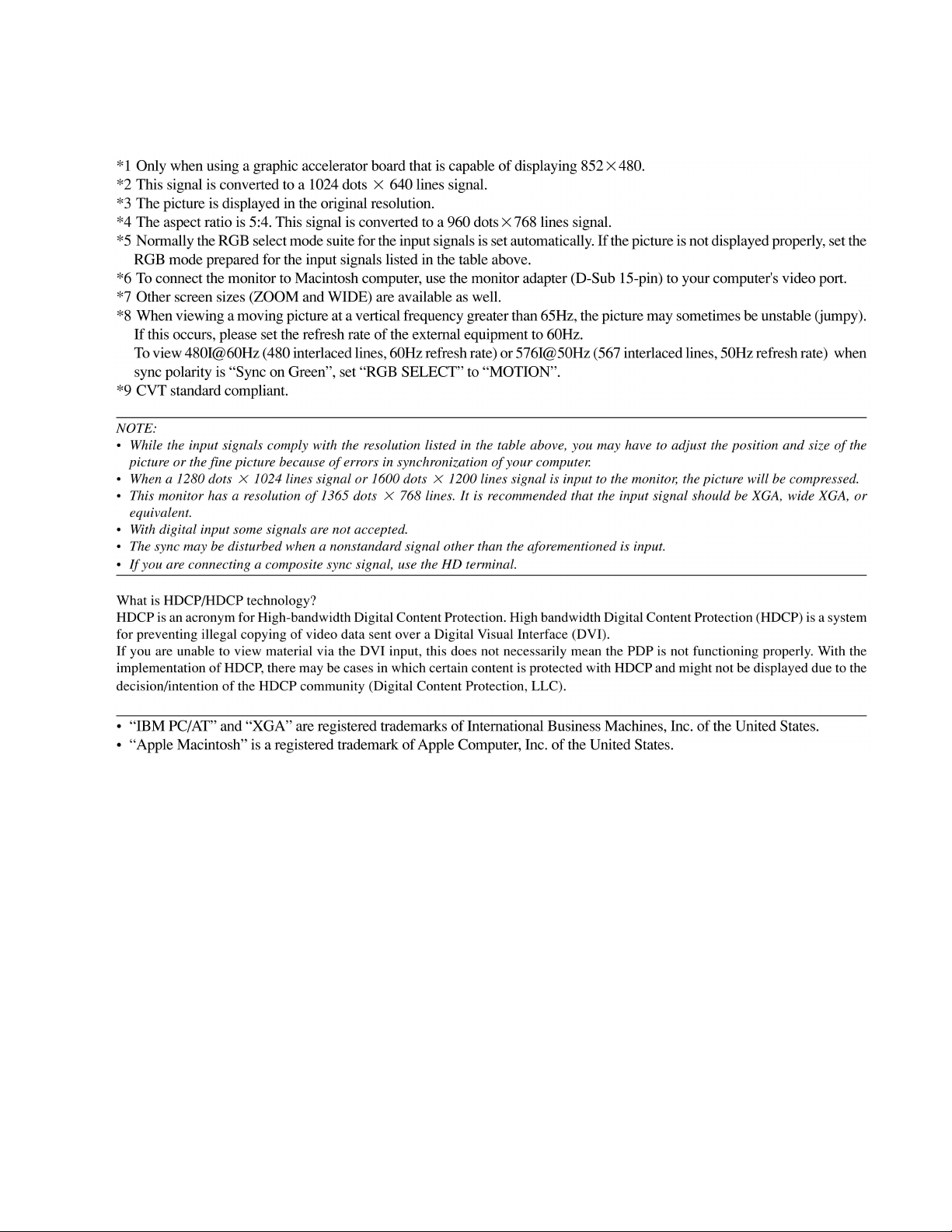
(Caution 1) For HDCP non-application products, the signals of the PC mode 1 ~ 89 can be received. For
HDCP application products, the signals of the PC mode 1 ~ 98 can be received.
(Caution 2) The received PC mode number specified below is displayed in the memory column of the user
menu “Information.”
PC mode 1 2 3 4 5
Signal name VU-6010
NTSC
Definition 640*240 768*288 640*400 640*480
Dot clock frequency (MHz) 12.214 14.752 25.175 25.175
H frequency (kHz) 15.734 15.557 31.469 31.469
V frequency (Hz) 59.94 50.39 70.086 59.94
63.534 64.262 31.778 31.778 H total (uS)
[a] (dots) 776 948 800 800
52.4 52.06 25.422 25.422 H display period (uS)
[d] (dots) 640 768 640 640
1.146 1.288 0.675 0.596 H front porch (uS)
[c] (dots)
[b] (dots) 107 128 64 96
[e] (dots)
14 19 17 15
8.76 8.677 2.542 3.813 H sync pulse width (uS)
1.228 2.237 3.138 1.946 H back porch (uS)
15 33 79 49
VU-6010
PAL/SECAM
NOT USED
PC98
400@70Hz
PC98
480@60Hz
16.652 20.055 14.268 16.683 V total (mS)
[f] (line) 262 312 449 525
15.3 18.513 12.711 15.253 V display period (mS)
[i] (line) 240 288 400 480
0.191 0.321 0.413 0.191 V front porch (mS)
[h] (line)
[g] (line) 18 17 2 2
[j] (line)
H sync polarity Neg Neg Neg Neg
V sync polarity Neg Neg Neg Neg
Scan type Interlaced Interlaced
Remarks
3 5 13 6
1.144 1.093 0.064 0.064 V sync pulse width (mS)
0.064 0.064 1.08 1.176 V back porch (mS)
1 1 34 37
Non Interlaced Non Interlaced
Page 72

9-12
PC mode 6 7 8 9 10
Signal name MAC@13" VESA
480@72Hz
Definition 640*480 640*480 640*480 640*480
Dot clock frequency (MHz) 30.24 31.5 31.5 36.0
H frequency (kHz) 35 37.861 37.5 43.269
V frequency (Hz) 66.667 72.809 75 85.008
28.571 26.413 26.667 23.111 H total (uS)
(dots) 864 832 840 832
21.164 20.317 20.317 17.778 H display period (uS)
(dots)
(dots) 64 24 16 56
(dots)
(dots) 96 128 120 80
640 640 640 640
2.116 0.762 0.508 1.556 H front porch (uS)
2.116 1.27 2.032 1.556 H sync pulse width (uS)
64 40 64 56
3.175 4.064 3.81 2.222 H back porch (uS)
VESA
480@75Hz
VESA
480@85Hz
NOT USED
15 13.735 13.333 11.764 V total (mS)
(line) 525 520 500 509
13.714 12.678 12.8 11.093 V display period (mS)
(line)
(line) 3 9 1 1
(line)
(line) 39 28 16 25
H sync polarity Sync on G Neg Neg Neg
V sync polarity Sync on G Neg Neg Neg
Scan type Non Interlaced Non Interlaced Non Interlaced Non Interlaced
Remarks
480 480 480 480
0.086 0.237 0.027 0.023 V front porch (mS)
0.086 0.079 0.08 0.069 V sync pulse width (mS)
3 3 3 3
1.114 0.739 0.427 0.578 V back porch (mS)
Page 73

9-13
PC mode 11 12 13 14 15
Signal name VESA
600@56Hz
Definition 800*600 800*600 800*600 800*600 800*600
Dot clock frequency (MHz) 36 40 50 49.5 56.25
H frequency (kHz) 35.156 37.879 48.077 46.875 53.674
V frequency (Hz) 56.25 60.317 72.188 75 85.061
28.444 26.4 20.8 21.333 18.631 H total (uS)
(dots) 1024 1056 1040 1056 1048
22.222 20 16 16.162 14.222 H display period (uS)
(dots)
(dots) 24 40 56 16 32
(dots)
(dots) 128 88 64 160 152
800 800 800 800 800
0.667 1 1.12 0.323 0.569 H front porch (uS)
2 3.2 2.4 1.616 1.138 H sync pulse width (uS)
72 128 120 80 64
3.556 2.2 1.28 3.232 2.702 H back porch (uS)
VESA
600@60Hz
VESA
600@72Hz
VESA
600@75Hz
VESA
600@85Hz
17.778 16.579 13.853 13.333 11.756 V total (mS)
(line) 625 628 666 625 631
17.067 15.84 12.48 12.8 11.179 V display period (mS)
(line)
(line) 1 1 37 1 1
(line)
(line) 22 23 23 21 27
H sync polarity Pos. Pos. Pos. Pos. Pos.
V sync polarity Pos. Pos. Pos. Pos. Pos.
Scan type Non Interlaced Non Interlaced Non Interlaced Non Interlaced Non Interlaced
Remarks
600 600 600 600 600
0.028 0.026 0.77 0.021 0.019 V front porch (mS)
0.057 0.106 0.125 0.064 0.056 V sync pulse width (mS)
2 4 6 3 3
0.626 0.607 0.478 0.448 0.503 V back porch (mS)
Page 74

9-14
PC mode 16 17 18 19 20
Signal name MAC@16" I/O data wide VESA wide
(NEC1)
Definition 832*624 852*480 848*480
Dot clock frequency (MHz) 57.2832 34.006 33.75
H frequency (kHz) 49.725 31.722 31.02
V frequency (Hz) 74.55 59.966 60
20.111 31.524 32.237 H total (uS)
(dots) 1152 1072 1088
14.524 25.055 25.126 H display period (uS)
(dots)
(dots) 32 22 16
(dots)
(dots) 224 70 112
(line) 667 529 517
(line)
(line) 1 12 6
(line)
832 852 848
0.559 0.659 0.474 H front porch (uS)
1.117 3.764 3.319 H sync pulse width (uS)
64 128 112
3.91 2.047 3.319 H back porch (uS)
13.414 16.676 16.667 V total (mS)
12.549 15.132 15.474 V display period (mS)
624 480 480
0.02 0.378 0.193 V front porch (mS)
0.06 0.095 0.258 V sync pulse width (mS)
3 3 8
0.784 1.072 0.741 V back porch (mS)
NOT USED
NOT USED
(line) 39 34 23
H sync polarity Sync on G Neg Pos.
V sync polarity Sync on G Neg Pos.
Scan type Non Interlaced Non Interlaced
Remarks
Non Interlaced
Page 75

9-15
PC mode 21 22 23 24 25
Signal name VESA wide
(NEC4)
Definition 1360*768 1024*768 1024*768
Dot clock frequency (MHz) 85.5 65 75
H frequency (kHz) 47.712 48.363 56.476
V frequency (Hz) 60.015 60.004 70.069
20.959 20.677 17.707 H total (uS)
(dots) 1792 1344 1328
15.906 15.754 13.653 H display period (uS)
(dots)
(dots) 64 24 24
(dots)
NOT USED
(dots) 256 160 144
1360 1024 1024
0.749 0.369 0.32 H front porch (uS)
1.31 2.092 1.813 H sync pulse width (uS)
112 136 136
2.994 2.462 1.92 H back porch (uS)
NOT USED
VESA
768@60Hz
VESA
768@70Hz
16.662 16.666 14.272 V total (mS)
(line) 795 806 806
16.097 15.88 13.599 V display period (mS)
(line)
(line) 3 3 3
(line)
(line) 18 29 29
H sync polarity Pos. Neg. Neg.
V sync polarity Pos. Neg. Neg.
Scan type
Remarks
768 768 768
0.063 0.062 0.053 V front porch (mS)
0.126 0.124 0.106 V sync pulse width (mS)
6 6 6
0.377 0.6 0.513 V back porch (mS)
Non Interlaced
Non Interlaced Non Interlaced
Page 76

9-16
PC mode 26 27 28 29 30
Signal name VESA
768@75Hz
Definition 1024*768 1024*768 1024*768 1280*1024 1280*1024
Dot clock frequency (MHz) 78.75 94.5 80 108 135
H frequency (kHz) 60.023 68.677 60.24 63.981 79.976
V frequency (Hz) 75.029 84.997 74.93 60.02 75.025
16.66 14.561 16.600 15.63 12.501 H total (uS)
(dots) 1312 1376 1328 1688 1688
13 10.836 12.8 11.852 9.481 H display period (uS)
(dots)
(dots) 16 48 32 48 2
(dots)
(dots) 176 208 176 248 248
1024 1024 1024 1280 1280
0.203 0.508 0.4 0.444 0.119 H front porch (uS)
1.219 1.016 1.2 1.037 1.067 H sync pulse width (uS)
96 96 96 112 144
2.235 2.201 2.2 2.296 1.837 H back porch (uS)
VESA
768@85Hz
MAC@19" VESA
1024@60Hz
VESA
1024@75Hz
13.328 11.765 13.347 16.661 13.329 V total (mS)
(line) 800 808 804 1066 1066
12.795 11.183 12.749 16.005 12.804 V display period (mS)
(line)
(line) 1 1 3 1 1
(line)
(line) 28 36 30 38 38
H sync polarity Pos. Pos. – Pos. Pos.
V sync polarity Pos. Pos. – Pos. Pos.
Scan type Non Interlaced Non Interlaced Non Interlaced Non Interlaced Non Interlaced
Remarks
768 768 768 1024 1024
0.017 0.015 0.050 0.016 0.013 V front porch (mS)
0.05 0.044 0.050 0.047 0.038 V sync pulse width (mS)
3 3 3 3 3
0.466 0.524 0.498 0.594 0.475 V back porch (mS)
Page 77

9-17
PC mode 31 32 33 34 35
Signal name IDC-3000G
PAL 625P
Definition 768*576 640*480 1920*1035 644*483 1280*720
Dot clock frequency (MHz) 29.687 24.39 74.25 24.37 74.25
H frequency (kHz) 31.389 31.47 33.75 31.469 45.000
V frequency (Hz) 50 59.9 60 59.94 60
31.933 31.775 29.63 31.777 22.222 H total (uS)
(dots) 948 775 2200 774 1650
25.87 26.24 25.86 26.427 17.239 H display period (uS)
(dots)
(dots) 8 10 44 18 70
(dots)
(dots) 97 65 192 55 220
768 640 1920 644 1280
0.269 0.41 0.59 0.75 0.943 H front porch (uS)
2.526 2.46 0.59 2.35 1.077 H sync pulse width (uS)
75 60 44 57 80
3.267 2.665 2.59 2.25 2.963 H back porch (uS)
IDC-3000G
NTSC 525P
HDTV-J DTV (480P) DTV (720P)
19.911 16.522 16.666 16.683 16.667 V total (mS)
(line) 625 525 562.5 525 750
18.35 15.106 15.348 15.348 16 V display period (mS)
(line)
(line) 7 8 5.5/5 6 5
(line)
(line) 35 30 35/34.5 30 20
H sync polarity Neg Neg Neg Neg Neg
V sync polarity Neg Neg Neg Neg Neg
Scan type Non Interlaced Non Interlaced Interlaced Non Interlaced Non Interlaced
Remarks
576 480 517/518 483 720
0.223 0.252 0.163/0.148 0.191 0.111 V front porch (mS)
0.223 0.22 0.148 0.191 0.111 V sync pulse width (mS)
7 7 5 6 5
1.115 0.944 1.037/1.022 0.953 0.444 V back porch (mS)
Page 78

9-18
PC mode 36 37 38 39 40
Signal name HDTV-W MAC@21" VESA
1024@85Hz
Definition 1920*1080 1152*870 1280*1024
Dot clock frequency (MHz) 74.25 100 157.5
H frequency (kHz) 33.75 68.681 91.146
V frequency (Hz) 60 75.062 85.024
29.630 14.560 10.971 H total (uS)
(dots) 2200 1456 1728
25.859 11.520 8.127 H display period (uS)
(dots)
(dots) 44 32 64
(dots)
(dots) 148 144 224
(line) 562.5 915 1072
(line)
(line) 2.5/2 3 1
(line)
1920 1152 1280
0.593 0.320 0.406 H front porch (uS)
1.185 1.280 1.016 H sync pulse width (uS)
88 128 160
1.993 1.440 1.422 H back porch (uS)
16.666 13.322 11.761 V total (mS)
16.000 12.667 11.235 V display period (mS)
540 870 1024
0.074/0.059 0.044 0.011 V front porch (mS)
0.148 0.044 0.033 V sync pulse width (mS)
5 3 3
0.444/0.459 0.568 0.483 V back porch (mS)
NOT USED NOT USED
(line) 15/15.5 39 44
H sync polarity Neg Sync on G Pos.
V sync polarity Neg Sync on G Pos.
Scan type Interlaced
Remarks
Non Interlaced Non Interlaced
Page 79

9-19
PC mode 41 42 43 44 45
Signal name I/O data
480@100Hz
Definition 640*480 640*480 800*600 800*600 1024*768
Dot clock frequency
(MHz)
H frequency (kHz) 51.089 61.307 62.998 75.703 80.451
V frequency (Hz) 100.370 120.440 99.838 119.97 100.56
(dots) 832 832 1048 1056 1392
(dots)
(dots) 64 64 40 24 24
(dots)
42.506 51.008 66.022 79.942 111.987
19.573 16.311 15.873 13.209 12.43 H total (uS)
15.057 12.574 12.117 10.007 9.144 H display period (uS)
640 640 800 800 1024
1.506 1.255 0.606 0.300 0.214 H front porch (uS)
1.317 1.098 0.969 1.001 0.786 H sync pulse width (uS)
56 56 64 80 88
1.694 1.412 2.181 1.901 2.286 H back porch (uS)
I/O data
480@120Hz
I/O data
600@100Hz
I/O data
600@120Hz
I/O data
768@100Hz
(dots) 72 72 144 152 256
9.963 8.302 10.016 8.335 9.944 V total (mS)
(line) 509 509 631 631 800
9.395 7.829 9.524 7.926 9.546 V display period (mS)
(line)
(line) 1 1 1 1 1
(line)
(line) 25 25 27 27 28
H sync polarity Neg Neg Pos. Pos. Neg
V sync polarity Neg Neg Pos. Pos. Neg
Scan type Non Interlaced Non Interlaced Non Interlaced Non Interlaced Non Interlaced
Remarks
480 480 600 600 768
0.020 0.016 0.016 0.013 0.012 V front porch (mS)
0.059 0.049 0.048 0.04 0.037 V sync pulse width (mS)
3 3 3 3 3
0.489 0.408 0.429 0.357 0.348 V back porch (mS)
Page 80

9-20
PC mode 46 47 48 49 50
Signal name I/O data
768@120Hz
Definition 1024*768 1280*1024 1280*1024 1920*1034 768*576
Dot clock frequency (MHz) 132.953 190.908 125 81 29.538
H frequency (kHz) 95.512 108.47 75.12 33.75 31.25
V frequency (Hz) 119.39 100.06 71.204 60 50
10.47 9.219 13.312 29.630 31.993 H total (uS)
(dots) 1392 1760 1664 2400 945
7.702 6.7 10.24 23.7 26 H display period (uS)
(dots)
(dots) 24 104 32 48 22
(dots)
(dots) 256 233 224 144 86
1024 1280 1280 1920 768
0.181 0.545 0.256 0.59 0.745 H front porch (uS)
0.662 0.75 1.024 3.56 2.35 H sync pulse width (uS)
88 143 128 288 69
1.925 1.22 1.792 1.78 2.9 H back porch (uS)
I/O data
1024@100Hz
EWS
4800@71Hz
RCA-STB
1080A
DTV(570P)
8.376 9.994 14.044 16.652 20 V total (mS)
(line) 800 1084 1055 562 625
8.041 9.44 13.631 15.319 18.432 V display period (mS)
(line)
(line) 1 1 3 2 5
(line)
(line) 28 56 25 40 39
H sync polarity Neg Pos. Neg Pos. Neg
V sync polarity Neg Pos. Neg Pos. Neg
Scan type Non Interlaced Non Interlaced Non Interlaced Interlaced Non Interlaced
Remarks
768 1024 1024 517 576
0.010 0.01 0.04 0.059 0.16 V front porch (mS)
0.031 0.03 0.04 0.089 0.16 V sync pulse width (mS)
3 3 3 3 5
0.293 0.52 0.333 1.185 1.248 V back porch (mS)
Page 81

9-21
PC mode 51 52 53 54 55
Signal name VESA
864@75Hz
Definition 1152*864 1280*768 1376*768 1600*1200 1600*1200
Dot clock frequency (MHz) 108 76.064 87.34 162 175.5
H frequency (kHz) 67.5 45.064 48.307 75 81.25
V frequency (Hz) 75 56.187 59.934 60 65
14.815 22.192 20.701 13.333 12.308 H total (uS)
(dots) 1600 1688 1808 2160 2160
10.667 16.828 15.755 9.877 9.117 H display period (uS)
(dots)
(dots) 64 48 32 64 64
(dots)
(dots) 256 248 272 304 304
1152 1280 1376 1600 1600
0.593 0.631 0.366 0.395 0.365 H front porch (uS)
1.185 1.472 1.466 1.185 1.094 H sync pulse width (uS)
128 112 128 192 192
2.37 3.26 3.114 1.877 1.732 H back porch (uS)
I/O data
W_XGA@56Hz
I/O wide
XGA
VESA
1200@60Hz
VESA
1200@65Hz
13.333 17.78 16.685 16.667 15.385 V total (mS)
(line) 900 802 806 1250 1250
12.8 17.043 15.898 16 14.769 V display period (mS)
(line)
(line) 1 2 3 1 1
(line)
(line) 32 29 29 46 46
H sync polarity Pos. Pos. Neg Pos. Pos.
V sync polarity Pos. Pos. Pos. Pos. Pos.
Scan type Non Interlaced Non Interlaced Non Interlaced Non Interlaced Non Interlaced
Remarks
864 768 768 1200 1200
0.015 0.044 0.062 0.013 0.012 V front porch (mS)
0.044 0.067 0.124 0.04 0.037 V sync pulse width (mS)
3 3 6 3 3
0.474 0.644 0.6 0.613 0.566 V back porch (mS)
Page 82

9-22
PC mode 56 57 58 59 60
Signal name VESA
1200@70Hz
Definition 1600*1200 1600*1200 1600*1200 1280*1024 1152*900
Dot clock frequency (MHz) 189 202.5 229.5 135 92.941
H frequency (kHz) 87.5 93.75 106.25 78.130 61.796
V frequency (Hz) 70 75 85 72.009 65.95
11.429 10.667 9.412 12.8 16.182 H total (uS)
(dots) 2160 2160 2160 1728 1504
8.466 7.901 6.972 9.481 12.395 H display period (uS)
(dots)
(dots) 64 64 64 64 29
(dots)
(dots) 304 304 304 192 195
1600 1600 1600 1280 1152
0.339 0.316 0.279 0.474 0.312 H front porch (uS)
1.016 0.948 0.837 1.442 1.377 H sync pulse width (uS)
192 192 192 192 128
1.608 1.501 1.325 1.442 2.098 H back porch (uS)
VESA
1200@75Hz
VESA
1200@85Hz
HP
1024@72Hz
SUN
900@66Hz
14.286 13.333 11.765 13.887 15.163 V total (mS)
(line) 1250 1250 1250 1085 937
13.714 12.8 11.294 13.107 14.564 V display period (mS)
(line)
(line) 1 1 1 3 2
(line)
(line) 46 46 46 55 31
H sync polarity Pos. Pos. Pos. SOG. Csync
V sync polarity Pos. Pos. Pos. SOG. Csync
Scan type Non Interlaced Non Interlaced Non Interlaced Non Interlaced Non Interlaced
Remarks
1200 1200 1200 1024 900
0.011 0.011 0.009 0.038 0.032 V front porch (mS)
0.034 0.032 0.028 0.038 0.065 V sync pulse width (mS)
3 3 3 3 4
0.526 0.491 0.433 0.704 0.502 V back porch (mS)
Page 83

9-23
PC mode 61 62 63 64 65
Signal name SUN
900@76Hz
Definition 1152*900 1024*768 1280*960 1280*960 1400*1050
Dot clock frequency (MHz) 105.561 70 108 148.5 108
H frequency (kHz) 71.710 49.716 60 85.938 63.981
V frequency (Hz) 76.047 60.043 60 85.002 60.020
13.945 20.114 16.667 11.636 15.630 H total (uS)
(dots) 1472 1408 1800 1728 1688
10.913 14.629 11.852 8.62 12.963 H display period (uS)
(dots)
(dots) 16 144 96 64 48
(dots)
(dots) 208 144 312 224 128
1152 1024 1280 1280 1400
0.152 2.057 0.889 0.431 0.444 H front porch (uS)
0.909 1.371 1.037 1.077 1.037 H sync pulse width (uS)
96 96 112 160 112
1.97 2.507 2.889 1.508 1.185 H back porch (uS)
SGI
768@60Hz
VESA
960@60Hz
VESA
960@60Hz
VESA
1050@60Hz
13.15 16.655 16.667 11.764 16.661 V total (mS)
(line) 943 828 1000 1011 1066
12.55 15.448 16 11.171 16.411 V display period (mS)
(line)
(line) 2 22 1 1 1
(line)
(line) 33 35 36 47 12
H sync polarity Csync SOG. Pos. Pos. Neg
V sync polarity Csync SOG. Pos. Pos. Neg
Scan type Non Interlaced Non Interlaced Non Interlaced Non Interlaced Non Interlaced
Remarks
900 768 960 960 1050
0.028 0.443 0.017 0.012 0.016 V front porch (mS)
0.112 0.06 0.05 0.035 0.047 V sync pulse width (mS)
8 3 3 3 3
0.460 0.704 0.6 0.547 0.188 V back porch (mS)
Page 84

9-24
PC mode 66~74
Signal name
Definition
Dot clock frequency (MHz)
H frequency (kHz)
V frequency (Hz)
H total (uS)
(dots)
H display period (uS)
(dots)
H front porch (uS)
(dots)
H sync pulse width (uS)
(dots)
H back porch (uS)
(dots)
V total (mS)
NOT USED
(line)
V display period (mS)
(line)
V front porch (mS)
(line)
V sync pulse width (mS)
(line)
V back porch (mS)
(line)
H sync polarity
V sync polarity
Scan type
Remarks
Page 85

9-25
PC mode 75 80 81 82 83
Signal name 1080I
50Hz
Definition 1920*1080 1280*768 720*400 720*350
Dot clock frequency (MHz) 74.25 81.0 28.3 28.3
H frequency (kHz) 28.125 47.99 31.5 31.5
V frequency (Hz) 50 59.34 70.1 70.1
35.556 20.84 31.78 31.78 H total (uS)
(dots) 2640 1688 900 900
25.859 15.80 25.42 25.42 H display period (uS)
(dots)
(dots) 484 48 18 18
(dots)
(dots) 148 248 54 54
1920 1280 720 720
6.519 0.593 0.636 0.636 H front porch (uS)
1.185 1.38 3.81 3.81 H sync pulse width (uS)
88 112 108 108
1.993 3.06 1.91 1.91 H back porch (uS)
W_XGA 400H 350H
NOT USED
10 16.713 14.269 14.269 V total (mS)
(line) 562.5 802 449 449
9.6 16.005 12.712 11.123 V display period (mS)
(line)
(line) 2.5/2 3 12 37
(line)
(line) 15/15.5 25 35 60
H sync polarity Neg. Pos. Neg. Pos.
V sync polarity Neg. Neg. Pos. Neg.
Scan type Interlaced Non Interlaced
Remarks
540 768 400 350
0.074/0.059 0.063 0.424 1.307 V front porch (mS)
0.148 0.125 0.064 0.064 V sync pulse width (mS)
5 6 2 2
0.444/0.459 0.521 1.112 1.907 V back porch (mS)
Non Interlaced Non Interlaced
Page 86

9-26
PC mode 84 85 86 87 88
Signal name 720P
24Hz
Definition 1280*720 1920*1080 1280*720 1920*1080
Dot clock frequency (MHz) 74.176 74.176 74.25 74.1758
H frequency (kHz) 17.982 26.973 37.5 26.973
V frequency (Hz) 23.976 23.976 50 37.074
55.611 37.704 26.667 37.074 H total (uS)
(dots) 4125 2750 1980 2750
17.256 25.884 17.239 25.884 H display period (uS)
(dots)
(dots) 2545 594 400 594
(dots)
(dots) 220 148 220 148
1280 1920 1280 1920
34.310 8.008 5.387 8.008 H front porch (uS)
1.078 1.078 1.078 1.078 H sync pulse width (uS)
80 88 80 88
2.256 1.995 2.963 1.995 H back porch (uS)
1080P
24Hz
720P
50Hz
1080I
48Hz
NOT USED
41.706 41.708 20 20.855 V total (mS)
(line) 750 1125 750 1125
40.040 40.040 19.2 20.020 V display period (mS)
(line)
(line) 5 4 5 5
(line)
(line) 20 36 20 30
H sync polarity Neg Neg Neg Neg
V sync polarity Neg Neg Neg Neg
Scan type Non Interlaced Non Interlaced Non Interlaced Interlaced
Remarks
720 1080 720 1080
0.278 0.148 0.133 0.093 V front porch (mS)
0.278 0.185 0.133 0.185 V sync pulse width (mS)
5 5 5 10
1.112 1.335 0.533 0.556 V back porch (mS)
Page 87

9-27
PC mode 89 90 91 92 93
Signal name 480i(60Hz) DTV(480P) DTV(480P) DTV(720P)
Definition 720*480Hz 640*480Hz 720*480Hz 1280*720Hz
Dot clock frequency (MHz) 27.000 25.175 27.000 74.250
H frequency (kHz) 15.734 31.469 31.469 45.000
V frequency (Hz) 59.94 59.940 59.94 60.000
16.555 31.777 31.777 22.222 H total (uS)
(dots) 1716 800 858 1650
53.333 25.422 26.666 17.239 H display period (uS)
(dots)
(dots) 38 16 16 110
(dots)
NOT USED
(dots) 114 48 60 220
(line) 262 525 525 750
(line)
(line) 4 10 9 5
(line)
1440 640 720 1280
1.407 0.635 0.592 1.481 H front porch (uS)
4.593 3.813 2.296 0.538 H sync pulse width (uS)
124 96 62 40
4.222 1.906 2.222 2.963 H back porch (uS)
16.635 16.683 19.444 10.101 V total (mS)
15.253 15.253 15.253 16.000 V display period (mS)
240 480 480 720
0.254 0.317 0.333 0.067 V front porch (mS)
0.191 0.064 0.191 0.111 V sync pulse width (mS)
3 2 6 5
0.953 1.049 0.953 0.444 V back porch (mS)
(line) 15 33 30 20
H sync polarity Neg Neg Neg Pos
V sync polarity Neg Neg Neg Pos
Scan type
Remarks HDCP* HDCP HDCP HDCP
*HDCP : High-bandwidth Digital Content Protection
Interlaced Non Interlaced Non Interlaced Non Interlaced
Page 88

9-28
PC mode 94 95 96 97 98
Signal name HDTV-W
Definition 1920*1080Hz
Dot clock frequency (MHz) 74.250
H frequency (kHz) 33.750
V frequency (Hz) 60.000
29.629 H total (uS)
(dots) 2200
25.859 H display period (uS)
(dots)
(dots) 88
(dots)
(dots) 148
1920
1.185 H front porch (uS)
0.592 H sync pulse width (uS)
44
1.993 H back porch (uS)
7.582 V total (mS)
NOT USED
(line) 563
16.000 V display period (mS)
(line)
(line) 3
(line)
(line) 15
H sync polarity Pos
V sync polarity Pos
Scan type Interlaced
Remarks HDCP
*HDCP : High-bandwidth Digital Content Protection
540
0.040 V front porch (mS)
0.148 V sync pulse width (mS)
5
0.444 V back porch (mS)
Page 89

(Caution) 1. Before disassembly, turn power off the main unit and pull out the power plug from the wall outlet.
10-1
METHOD OF DISASSEMBLY
2. Use a screwdriver with a fitting size. Otherwise, the screw threads may be damaged.
3. Reassembly can be carried out in the reverse order for disassembly. Refer to the disassembly procedures and forward
reassembly in the reverse order.
4. The order for taking out the parts (or components) is indicated by the foregoing numeral that is attached to the name of
each part.
5. The wire connector symbol is indicated by two digits of Marking . Read CN- when examining the table of parts.
6. Class A or Class B in the text is applicable to the models specified below.
CLASS A: PX-61XM3J,61XM3A,61XM3W,61XM3G, CLASS B: PDP-614MX,PRO-1410HD,PX-61XR3A,61XR3W,61XR3G
1. Outlined method of disassembly
The outlined procedures for the disassembly of the major parts are shown below (disassembled in the direction of ).
In regard to the details of disassembly, cautions, etc., refer to the method of replacement for each part [page indicated in ( )].
SET
(with a STAND)
SET
(without a STAND)
* Modification means that the screws
are mounted or removed.
STAND
(P10-2)
Modifications of
a STAND *
(P10-11)
BACK COVER
(P10-3)
Modifications of
a BACK COVER *
(P10-12)
BACK COVER
(P10-3)
CHASSIS ASSY
(P10-4)
FRONT PANEL
(P10-10)
F-BRACKET B(OUT)
TERMINAL PANEL M SUB ASSY
(P10-13)
TERMINAL PANEL S
(P10-15)
COVER SW
(P10-16)
TERMINAL PANEL B SUB ASSY
(P10-17)
POWER UNIT
(P10-19)
SEND PWB
(P10-20)
SENB PWB
SENC PWB
PDP
(P10-5)
(P10-9)
(P10-20)
(P10-20)
F-BRACKET(IN)
(P10-6)
F-BRACKET(OUT) ASSY
(P10-8)
LED PWB
(P10-9) (P10-9)
CTL PWB
(P10-9)
TERMINAL PANEL M
(P10-14)
232C PWB
(P10-15)
POWER BUTTON
(P10-16)
TERMINAL PANEL B
(P10-18)
FAN
(P10-20)
COVER CTL
FILTER
(P10-6∼10-7)
CONTROL BUTTON
(P10-9)
MAIN PWB
(P10-14)
PWR PWB
(P10-16)
AUDIO PWB
(P10-18)
AC INLET
(P10-18)
Page 90

2. STAND
10-2
(1)SRW32
(1)SRW32
(1)SCREW M6*50 4p
(1)SCREW M6*50 4p
CBIPS*4*12*15KF
CBIPS*4*12*15KF
24N04471 *12p
24N04471 *12p
(2)PX-61ST1U-ST
(2)PX-61ST1U-ST
Page 91

3. BACK COVER
10-3
(5)SRW33
(5)SRW33
PL-CPIMS*4*12*15KFE
PL-CPIMS*4*12*15KFE
29N01431 *14p
29N01431 *14p
(1)SRW34
(1)SRW34
PL-CPIMS*4*16*3KF
PL-CPIMS*4*16*3KF
910E4066 *4p
910E4066 *4p
M31 GS COVER
M31 GS COVER
29H02782
29H02782
(Caution) Replacement is
(Caution) Replacement is
impossible unless the NAME
impossible unless the NAME
PLATE is removed.
PLATE is removed.
M03 SERIAL LABEL
M03 SERIAL LABEL
24L44731
24L44731
(Caution) This is not a service part.
(Caution) This is not a service part.
M56 SPEAKER LABEL
M56 SPEAKER LABEL
29L03552
29L03552
(3)SRW35 PL-CPIMS*3*10*15KFE
(3)SRW35 PL-CPIMS*3*10*15KFE
29N01431 *14p
29N01431 *14p
(4)SRW32
(4)SRW32
CBIPS*4*12*15KFE
CBIPS*4*12*15KFE
29N01401 *12p
29N01401 *12p
M57 NAME PLATE
M57 NAME PLATE
M55 AC IN LABEL
M55 AC IN LABEL
29L00491
29L00491
(2)M18 HANDLE
(2)M18 HANDLE
29F00591 *2p
29F00591 *2p
(6)M58 BACK COVER(61XM2)
(6)M58 BACK COVER(61XM2)
29P01271
29P01271
M63 LABEL(EARTH)
M63 LABEL(EARTH)
24L44791
24L44791
(Caution) To be used only for the PX-61XM3.
(Caution) To be used only for the PX-61XM3.
Page 92

4. CHASSIS ASSY
10-4
(6)SRW05,06 PL-CPIMS*6*20*15KFE
(6)SRW05,06 PL-CPIMS*6*20*15KFE
29N01451 *10p
29N01451 *10p
(7)SRW07,08,09,11,13
(7)SRW07,08,09,11,13
PL-CPIMS*4*12*15KFE
PL-CPIMS*4*12*15KFE
29N01441 *22p
29N01441 *22p
(4)CONNECTOR
(4)CONNECTOR
(5)CONNECTOR 4p
(5)CONNECTOR 4p
(Caution) Remove the ferrite
(Caution) Remove the ferrite
core first.
core first.
(3)SRW17 TP-M3*6*3KF
(3)SRW17 TP-M3*6*3KF
24N04581
24N04581
(Caution) For mounting, it should
(Caution) For mounting, it should
be tightened together with the
be tightened together with the
round terminal of the AD cable.
round terminal of the AD cable.
(8)CHASSIS ASSY
(8)CHASSIS ASSY
(2)M40 SHIELD COVER MAIN
(2)M40 SHIELD COVER MAIN
29H03021
29H03021
(1)SRW31 PL-CPIMS*4*12*15KFE
(1)SRW31 PL-CPIMS*4*12*15KFE
29N01481 *8p
29N01481 *8p
Page 93

5. PDP
10-5
(4)CN-PH CN 9P(PH) 360W,1007-20
(4)CN-PH CN 9P(PH) 360W,1007-20
7SW9W008
7SW9W008
(3)CN-PD CN 10P(PD) 920W,1007-20
(3)CN-PD CN 10P(PD) 920W,1007-20
7SW0W010
7SW0W010
(5)PDP PDP-NP61C2MF01AA
(5)PDP PDP-NP61C2MF01AA
3S361002
3S361002
(2)CN-AD CABLE 31P L390
(2)CN-AD CABLE 31P L390
(1) SCREW
(1) SCREW
(Caution) This screw is used
(Caution) This screw is used
to fasten the PWB of the PDP.
to fasten the PWB of the PDP.
The right bottom corner is regarded
The right bottom corner is regarded
as the mounting basis.
as the mounting basis.
7S530036
7S530036
Page 94

6. F-BRACKET(IN) /FILTER
10-6
(Caution) Once the shielding tape and the cushion are removed, they must not be used again because their adhesive
strength has been reduced.
(4)M33 F-BRACKET T(IN)
(4)M33 F-BRACKET T(IN)
29H02951
29H02951
29H02941 2p
29H02941 2p
M48 CUSHION(782*10*T5)
M48 CUSHION(782*10*T5)
29J01171 *2p
29J01171 *2p
* Used in common for right and left
* Used in common for right and left
M49 CUSHION(686*10*T5)
M49 CUSHION(686*10*T5)
29J01181 *4p
29J01181 *4p
* Used in common for top and bottom
* Used in common for top and bottom
(2)M32 F-BRACKET LR(IN)
(2)M32 F-BRACKET LR(IN)
* Used in common for right and left
* Used in common for right and left
(3)M34 F-BRACKET B(IN)
(3)M34 F-BRACKET B(IN)
29H02961
29H02961
(5)M54 FILTER
(5)M54 FILTER
CLASS A : 29KS0211
CLASS A : 29KS0211
CLASS B : 29KS0171
CLASS B : 29KS0171
M04 EDGING SADDLE(EDS-1208U)
M04 EDGING SADDLE(EDS-1208U)
29C00461 *2p
29C00461 *2p
(Caution) The filter is standardized to be positioned at bottom left.
(Caution) The filter is standardized to be positioned at bottom left.
M62 SHIELDING TAPE (25MM*50M)
M62 SHIELDING TAPE (25MM*50M)
The 29C01911 shall be stuck to the four sides. (CLASS A only)
The 29C01911 shall be stuck to the four sides. (CLASS A only)
(1)SRW04 PL-CPIMS*3*6*15KFE
(1)SRW04 PL-CPIMS*3*6*15KFE
29N01421 *30p
29N01421 *30p
Page 95

7. FILTER(CLASS A)
10-7
(Caution) No SHIELDING TAPE has been stuck to the service part FILTER. Therefore, in the case of filter replacement,
please order the SHIELDING TAPE and stick it as illustrated below.
(Caution) Once the shielding tape is removed, it must not be used again because its adhesive strength has been reduced.
SHIELDING TAPE
(Caution) Once the shielding tape is removed, it must not be used again because its adhesive strength has been reduced.
1366mm
Spatter film
[Display side]
Silver paste
FILTER
[Display side]
Black area
776mm
Cross-section diagram
M62 SHIELDING TAPE AL(25MM*50M)
29C01911
Page 96

8. F-BRACKET(OUT) ASSY
10-8
M20 CORNER PIECE LT
29F00731
(Caution) Insertion is possible by sliding it
(Caution) Insertion is possible by sliding it
from bottom to top.
from bottom to top.
(1)F-BRACKET (OUT) ASSY
(1)F-BRACKET (OUT) ASSY
(2)FRONT PANEL ASSY
(2)FRONT PANEL ASSY
M21 CORNER PIECE RT
(Caution) Insertion is possible by sliding it
(Caution) Insertion is possible by sliding it
from bottom to top.
from bottom to top.
M36 F-BRACKET T(OUT)
M36 F-BRACKET T(OUT)
29H02981
29H02981
29F00741
SRW03 CBIPS*4*12*15KFE
29N01401 *8p
M37 F-BRACKET B(OUT)
29H02991
M22 CORNER PIECE LB
M22 CORNER PIECE LB
29F00751
29F00751
(Caution) Insertion is possible by sliding it
(Caution) Insertion is possible by sliding it
from top to bottom.
from top to bottom.
M37 F-BRACKET B(OUT)
29H02991
Cross section A-A
A
A
Double-coated adhesive tape
M35 F-BRACKET LR(OUT)
29H02971 *2p
* Used in common for right and
* Used in common for right and
left
left
M72 CUHSION(FILTER)
29J01331*3p
*Stuck so that it touches the bottom wall.
M23 CORNER PIECE RB
M23 CORNER PIECE RB
29F00761
29F00761
(Caution) Insertion is possible by sliding it
(Caution) Insertion is possible by sliding it
from top to bottom.
from top to bottom.
M72 CUHSION(FILTER)
29J01331*3p
*Stuck almost in the midst of the neighboring studs
Page 97

9. LED PWB/CTL PWB/F-BRACKET B(OUT)/COVER CTL/CONTROL BUTTON
10-9
(5)CONNECTOR
(5)CONNECTOR
(6)SRW02 TP-M3*6*3KF
(6)SRW02 TP-M3*6*3KF
(2)A03 CTL PWB ASSY
(2)A03 CTL PWB ASSY
937F7SB1
937F7SB1
(3) M26 CLASS A CONTROL BUTTON:29G00311
(3) M26 CLASS A CONTROL BUTTON:29G00311
CLASS B CONTROL BUTTON-S:29G00331
CLASS B CONTROL BUTTON-S:29G00331
(4)M24 CLASS A COVER CTL:29F00781
(4)M24 CLASS A COVER CTL:29F00781
CLASS B COVER CTL-S:29F00801
CLASS B COVER CTL-S:29F00801
(Caution) For reassembly, put the CONTROL BUTTON in the
(Caution) For reassembly, put the CONTROL BUTTON in the
clearance and screw-fasten the CTL PWB to the F-BRACKET.
clearance and screw-fasten the CTL PWB to the F-BRACKET.
24N04581 *2p
24N04581 *2p
(8)CONNECTOR
(8)CONNECTOR
(7)A05 LED PWB ASSY
(7)A05 LED PWB ASSY
937F7SD1
937F7SD1
(1)SRW01 TP-M3*6*3KF
(1)SRW01 TP-M3*6*3KF
24N04581 *3p
24N04581 *3p
(10)M37 F-BRACKET B(OUT)
29H02991
(9)M10 CLAMP(UAMS-05-2)
(9)M10 CLAMP(UAMS-05-2)
29C01751 *7p
29C01751 *7p
FRONT PANEL ASSY
FRONT PANEL ASSY
Page 98

10. FRONT PANEL
10-10
(1)M50 INDICATOR(50XM3)
(1)M50 INDICATOR(50XM3)
29K00421
29K00421
(Caution) For removal, it comes off when it is pressed
(Caution) For removal, it comes off when it is pressed
strongly from the rear side of the front panel. For installation,
strongly from the rear side of the front panel. For installation,
remove the separator before adhesion.
remove the separator before adhesion.
(2)M16 CLASS A FRONT PANEL(61XM2) :29D00612
(2)M16 CLASS A FRONT PANEL(61XM2) :29D00612
CLASS B FRONT PANEL(61XM2/S):29D00633
CLASS B FRONT PANEL(61XM2/S):29D00633
Page 99

11. STAND (modification)
10-11
(6) Fit it, using the screw that
(6) Fit it, using the screw that
has been removed as per (1).
has been removed as per (1).
(Caution) The screw can
(Caution) The screw can
be tightened only midway.
be tightened only midway.
(1)SRW32
(1)SRW32
(1)SCREW M6*50 2p*2
(1)SCREW M6*50 2p*2
CBIPS*4*12*15KF
CBIPS*4*12*15KF
24N04471 *12p
24N04471 *12p
(3)COVER POST 1p*2
(3)COVER POST 1p*2
(2) PL-CPIMS*4*12*15KF 1p*2
(2) PL-CPIMS*4*12*15KF 1p*2
(5)POST 1p*2
(5)POST 1p*2
(4)HEXAGONAL BOLT 3p*2
(4)HEXAGONAL BOLT 3p*2
(Caution) Use a hexagon head
(Caution) Use a hexagon head
wrench (opposite side distance 5mm).
wrench (opposite side distance 5mm).
Page 100

12. BACK COVER (modification)
10-12
(Caution) The illustration below shows a case when the STAND has been removed.
(1)SRW32
(1)SRW32
CBIPS*4*12*15KFE
CBIPS*4*12*15KFE
29N01401 *12p
29N01401 *12p
(2)FRONT PANEL ASSY
(2)FRONT PANEL ASSY
 Loading...