

Page 1
PDP-508XG
PLASMA TELEVISION
PDP-508XG
PDP-508XDA
PDP-508XC
THIS MANUAL IS APPLICABLE TO THE FOLLOWING MODEL(S) AND TYPE(S).
Model Type Power Requirement Remarks
PDP-508XG DLFT AC 110 V to 240 V
PDP-508XDA YP AC 240 V
PDP-508XC WA5 AC 220 V to 240 V
ORDER NO.
ARP3468
This service manual should be used together with the following manual(s):
Model Order No. Remarks
PDP-5080XA/WYV5 ARP3445 EXPLODED VIEWS, BLOCK DIAGRAM, ADJUSTMENT, etc
For SPECIFICATIONS and PANEL FACILITIES, refer to the operating instructions.
PIONEER CORPORATION 4-1, Meguro 1-chome, Meguro-ku, Tokyo 153-8654, Japan
PIONEER ELECTRONICS (USA) INC. P.O. Box 1760, Long Beach, CA 90801-1760, U.S.A.
PIONEER EUROPE NV Haven 1087, Keetberglaan 1, 9120 Melsele, Belgium
PIONEER ELECTRONICS ASIACENTRE PTE. LTD. 253 Alexandra Road, #04-01, Singapore 159936
PIONEER CORPORATION 2007
T-ZZK-001 AUG. 2007 printed in Japan
Page 2

1234
CONTENTS
1. CONTRAST OF MISCELLANEOUS PARTS.................................................................................................... 4
2. BASIC ITEMS FOR SERVICE.......................................................................................................................... 8
A
B
C
D
E
F
2.1 QUICK REFERENCE.................................................................................................................................8
3. BLOCK DIAGRAM.......................................................................................................................................... 10
3.1 OVERALL WIRING DIAGRAM (1/2) ........................................................................................................ 10
3.2 OVERALL WIRING DIAGRAM (2/2) ........................................................................................................ 12
3.3 OVERALL BLOCK DIAGRAM .................................................................................................................. 14
3.4 POWER SUPPLY BLOCK of MULTI BASE SECTION ............................................................................. 16
3.5 TANSHI ASSY .......................................................................................................................................... 18
3.6 POWER SUPPLY BLOCK of 50LED&IR&RLS and SIDE KEY ASSYS ................................................... 19
4. DIAGNOSIS.................................................................................................................................................... 20
4.1 POWER SUPPLY OPERATION ...............................................................................................................20
4.1.1 LED DISPLAY INFORMATION ........................................................................................................... 20
4.1.2 POWER ON SEQUENCE................................................................................................................... 21
4.1.3 DETAILS OF POWER ON SEQUENCE ............................................................................................. 22
4.2 DIAGNOSIS FLOWCHART OF FAILURE ANALYSIS.............................................................................. 26
4.2.1 VIDEO SYSTEM ................................................................................................................................. 26
4.2.2 AUDIO SYSTEM ................................................................................................................................. 27
4.3 DIAGNOSIS OF SD (SHUTDOWN) ......................................................................................................... 30
4.3.1 SD (SHUTDOWN) DIAGNOSIS.......................................................................................................... 30
4.4 NON-FAILURE INFORMATION ............................................................................................................... 31
4.4.1 INFORMATION ON SYMPTOMS THAT DO NOT CONSTITUTE FAILURE....................................... 31
4.5 OUTLINE OF THE OPERATION.............................................................................................................. 35
4.5.1 SPECIFICATION OF THE FAN CONTROL ........................................................................................ 35
5. SERVICE FACTORY MODE........................................................................................................................... 36
5.1 OUTLINE OF THE SERVICE FACTORY MODE...................................................................................... 36
5.1.1 REMOTE CONTROL CODE IN SERVICE FACTORY MODE ............................................................ 36
5.1.2 INDICATIONS IN SERVICE FACTORY MODE................................................................................... 37
5.2 DETAILS OF FACTORY MENU................................................................................................................ 38
5.2.1 INFORMATION ................................................................................................................................... 38
5.2.2 OPTION .............................................................................................................................................. 41
6. EACH SETTING AND ADJUSTMENT............................................................................................................ 42
6.1 ADJUSTMENT REQUIRED WHEN THE UNIT IS REPAIRED OR REPLACED...................................... 42
7. RS-232C ......................................................................................................................................................... 43
7.1 LIST OF RS-232C COMMANDS.............................................................................................................. 43
7.2 DETAILS OF EACH COMMANDS ........................................................................................................... 44
7.2.1 QSE (DESTINATION PECULIAR INFORMATION)............................................................................. 44
7.2.2 QNG (SHUTDOWN INFORMATION OF MTB) ................................................................................... 45
8. GENERAL INFORMATION ............................................................................................................................. 47
8.1 DISPLAY METHOD OF SIGNAL LEVEL,QUALTY,AND BER INFORMATION SCREEN ........................ 47
9. SCHEMATIC DIAGRAM ................................................................................................................................. 48
9.1 MAIN ASSY (1/20) [BOARD IF0 BLOCK] ................................................................................................ 48
9.2 MAIN ASSY (2/20) [BOARD IF1 BLOCK] ................................................................................................ 50
9.3 MAIN ASSY (3/20) [POWER 0 BLOCK]................................................................................................... 52
9.4 MAIN ASSY (4/20) [POWER 1 BLOCK]................................................................................................... 54
9.5 MAIN ASSY (5/20) [POWER 2 BLOCK]................................................................................................... 56
9.6 MAIN ASSY (6/20) [AV SW BLOCK]........................................................................................................ 58
9.7 MAIN ASSY (7/20) [RGB SW BLOCK]..................................................................................................... 60
9.8 MAIN ASSY (8/20) [VDEC BLOCK]......................................................................................................... 62
9.9 MAIN ASSY (9/20) [ADC BLOCK]............................................................................................................ 64
9.10 MAIN ASSY (10/20) [HDMI SW BLOCK] ............................................................................................... 66
9.11 MAIN ASSY (11/20) [HDMI BLOCK]......................................................................................................68
9.12 MAIN ASSY (12/20) [TUNER BLOCK]................................................................................................... 70
9.13 MAIN ASSY (13/20) [VBI SLICER BLOCK] ........................................................................................... 72
9.14 MAIN ASSY (14/20) [USB BLOCK]........................................................................................................ 74
9.15 MAIN ASSY (15/20) [ARIA 0 BLOCK].................................................................................................... 76
9.16 MAIN ASSY (16/20) [ARIA 1 BLOCK].................................................................................................... 78
9.17 MAIN ASSY (17/20) [ARIA MEMORY BLOCK]......................................................................................80
9.18 MAIN ASSY (18/20) [IF UCOM BLOCK] ................................................................................................ 82
9.19 MAIN ASSY (19/20) [EMMA2 BLOCK] .................................................................................................. 84
9.20 MAIN ASSY (20/20) [EMMA2 MEMORY BLOCK] ................................................................................. 86
9.21 TANSHI ASSY (1/4) [BOARD IF BLOCK] .............................................................................................. 88
9.22 TANSHI ASSY (2/4) [IO_1 BLOCK]........................................................................................................ 90
9.23 TANSHI ASSY (3/4) [IO_2 BLOCK]........................................................................................................ 92
9.24 TANSHI ASSY (4/4) [MSP BLOCK]........................................................................................................ 94
2
1 234
PDP-508XG
Page 3

5678
9.25 SIDE IO ASSY........................................................................................................................................96
9.26 DTV TUNER BOARD (1/16) [DDR TERM/CONN BLOCK] ....................................................................98
9.27 DTV TUNER BOARD (2/16) [DDR-SDRAM BLOCK]...........................................................................100
9.28 DTV TUNER BOARD (3/16) [DVO, PIN STRAPOPTION BLOCK].......................................................102
9.29 DTV TUNER BOARD (4/16) [AUDIO BUFFER BLOCK] ......................................................................104
9.30 DTV TUNER BOARD (5/16) [VIDEO DAC OUTPUT BLOCK] .............................................................106
9.31 DTV TUNER BOARD (6/16) [DVO BLOCK] .........................................................................................108
9.32 DTV TUNER BOARD (7/16) [PCI BLOCK]...........................................................................................110
9.33 DTV TUNER BOARD (8/16) [EBI, RESET BLOCK] .............................................................................112
9.34 DTV TUNER BOARD (9/16) [I2C, UART, CLK BLOCK] .......................................................................114
9.35 DTV TUNER BOARD (10/16) [EJTAG, TS, EEPROM BLOCK]............................................................116
9.36 DTV TUNER BOARD (11/16) [USB;ETHERNET;SATA BLOCK]..........................................................118
9.37 DTV TUNER BOARD (12/16) [POWER BLOCK] .................................................................................120
9.38 DTV TUNER BOARD (13/16) [ANALOG DECOUPLING BLOCK] .......................................................122
9.39 DTV TUNER BOARD (14/16) [VIDEO BUFFERS, DIGITAL DECOUPLING BLOCK]..........................124
9.40 DTV TUNER BOARD (15/16) [FRONT END BLOCK]..........................................................................126
9.41 DTV TUNER BOARD (16/16) [INTER-CONNECTION BLOCK]...........................................................128
9.42 VOLTAGES ...........................................................................................................................................130
10. PCB CONNECTION DIAGRAM..................................................................................................................134
10.1 MAIN ASSY ..........................................................................................................................................134
10.2 TANSHI ASSY ......................................................................................................................................138
10.3 SIDE IO ASSY......................................................................................................................................142
10.4 DTV TUNER BOARD ...........................................................................................................................144
11. PCB PARTS LIST........................................................................................................................................146
A
B
C
D
E
PDP-508XG
56
F
3
7
8
Page 4
1234
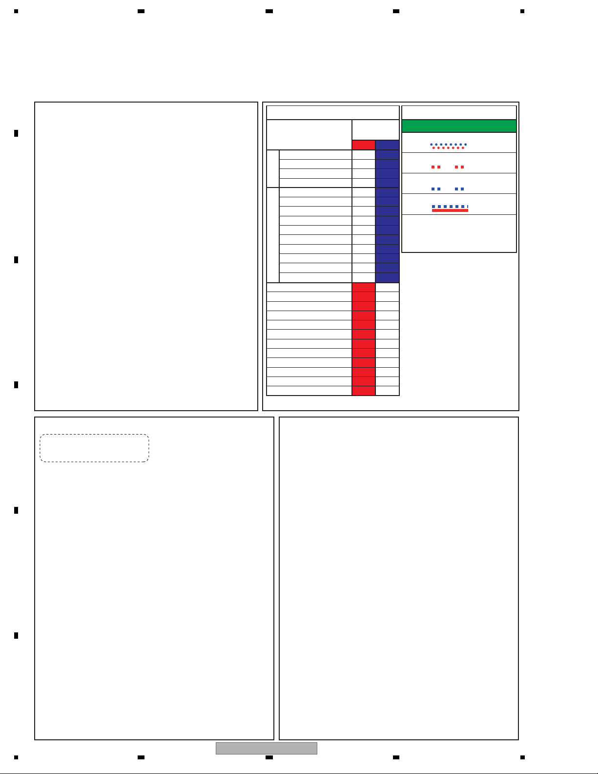
1. CONTRAST OF MISCELLANEOUS PARTS
NOTES:
A
Parts marked by "NSP" are generally unavailable because they are not in our Master Spare Parts List.
The mark found on some component parts indicates the importance of the safety factor of the part.
Therefore, when replacing, be sure to use parts of identical designation.
Screws adjacent to mark on product are used for disassembly.
For the applying amount of lubricants or glue, follow the instructions in this manual.
(In the case of no amount instructions, apply as you think it appropriate.)
Nos. indicate the pages and Nos. in the service manual for the base model.
When ordering resistors, first convert resistance values into code form as shown in the following examples.
Ex.1 When there are 2 effective digits (any digit apart from 0), such as 560 ohm and 47k ohm (tolerance is shown by J=5%,
and K=10%).
B
Ex.2 When there are 3 effective digits (such as in high precision metal film resistors).
56 x 10
47 x 103
R50
1R0
1
561
473
1
5621 5 26 1
RD1/4PU J
RD1/4PU J
RN2H K
RS1P K
5
4 7 3
R 5 0
R 0
1
6 1
RN1/4PC F562 x 10
CONTRAST TABLE
PDP-508XD/WYV5, PDP-508XG/DLFT, PDP-508XDA/YP and PDP-508XC/WA5 are constructed the same except
for the following:
Mark No. Symbol and Description
PCB ASSEMBLIES
P173-1 MAIN Assy AWV2461 AWV2465 AWV2465 AWV2466
NSP 1..FUKUGO Assy AWV2481 AWV2491 AWV2489 AWV2491
C
P173-2 2..TANSHI ASSY AWW1248 AWW1258 AWW1256 AWW1258
P163-1 2..SIDE IO ASSY AWW1253 AWW1259 AWW1259 AWW1259
P173-3 2..232C ASSY AWW1254 Not used Not used Not used
PDP-508XD
/WYV5
PDP-508XG
/DLFT
PDP-508XDA
/YP
PDP-508XC
/WA5
Remarks
NSP 1..50 DIGITAL ASSY AWV2445 AWV2533 AWV2533 AWV2533
P169-3 2..50 DIGITAL ASSY AWW1270 AWW1337 AWW1337 AWW1337
DTV TUNER BOARD Not used Not used AXY1170 Not used *1 No. 1
PACKING SECTION
>
NSP P161-5 Dry Cell Battery (R06, AA) VEM1031 AEX1025 VEM1031 VEM1031
D
NSP P161-13 Warranty Card ARY1204 Not used ARY1192 ARY1161
NSP P161-15 Catalogue Bag AHG1340 Not used Not used
E
P161-1 Power Cord (2 m) ADG1214 Not used ADG1245 ADG1209
P161-3 Remote Control Unit AXD1551 AXD1554 AXD1555 AXD1556
P161-9 Operating Instructions
(English/French/German)
P161-10 Operating Instructions
(Italian/Spanish/Dutch)
P161-11 Caution Card ARM1232
P161-14 Polyethylene Bag AHG1337 AHG1337 AHG1336 AHG1336
P161-21 Power Cord Lid AHC1085 AHC1085 Not used Not used
P161-23 Upper Carton AHD3646 AHD3606 AHD3607 AHD3608
P161-25 After Image Caution ARM1350 Not used Not used Not used
Operating Instructions
(Simp-Chinese)
Operating Instructions (English) Not used Not used ARB1577 Not used
Operating Instructions
(English/Spanish/Portuguese
/Trad-Chinese)
ARE1484 Not used Not used Not used
ARC1601 Not used Not used Not used
ARM1232 ARM1232
Not used Not used Not used ARC1581
Not used ARE1479 Not used Not used
Not used
AHG1340
>
NSP Power Cord Not used ADG1232 Not used Not used
>
NSP
>
NSP
>
NSP
F
>
NSP
>
NSP
>
NSP
4
Power Cord Not used ADG1234 Not used Not used
Power Cord Not used ADG1236 Not used Not used
Power Cord Not used ADG1239 Not used Not used
Power Cord Not used ADG1241 Not used Not used
Power Cord Not used ADG1242 Not used Not used
Power Cord Not used ADG1243 Not used Not used
PDP-508XG
1 234
Page 5
5678
Mark No. Symbol and Description
>
NSP
>
NSP
>
NSP
Power Cord Not used ADG1244 Not used Not used
Power Cord Not used ADG1246 Not used Not used
Power Cord Assy Not used AWX1095 Not used Not used
PDP-508XD
/WYV5
PDP-508XG
/DLFT
PDP-508XDA
/YP
PDP-508XC
/WA5
PAL RF Cable (30cm) Not used Not used ADF1036 Not used
Caution Card (PC) Not used Not used Not used ARM1302
REAR SECTION
NSP P163-17 Name Label AAL3005 AAL3011 AAL3012 AAL3014
P163-19 Bolt Caution Label (E) AAX3533
AAX3533 AAX3533 AAX3550
P163-20 Label A AAX3480 AAX3485 AAX3484 AAX3485
P163-21 Label B50 AAX3543 AAX3500 AAX3520 AAX3500
P163-22 Label C AAX3504 AAX3507 AAX3521 AAX3507
Remarks
A
P163-23 Terminal Panel B ANC2454 ANC2456 ANC2456 ANC2456
P163-28 Input Cover Label E AAX3510 AAX3511 AAX3511 AAX3511
P163-38 Screw BPZ30P080FTB Not used Not used Not used
Destination Label O Not used AAX3446 Not used Not used No. 2
NSP CCC S&E Label Not used Not used Not used DRW2310 No. 3
Screw Not used BBZ30P060FTB BBZ30P060FTB BBZ30P060FTB No. 15
FRONT SECTION
P165-12 Front Case Assy AMB3025 AMB3026 AMB3027 AMB3026
MULTI BASE SECTION
P173-7 Flexible Cable (J217) ADD1494 Not used Not used Not used
P173-20 POD Cover AMR3542 Not used Not used Not used
P173-21 Multi Base Assy ANA2103 ANA2103 ANA2104 ANA2103
P173-22 Terminal Panel A ANC2441 ANC2445 ANC2446 ANC2445
12P Housing Wire (J131) Not used Not used ADX3549 Not used No. 4
Flexible Cable (J219) Not used Not used ADD1450 Not used No. 5
Flexible Cable (J220) Not used Not used ADD1497 Not used No. 6
NSP Bottom Can Not used Not used XNA1005 Not used No. 7
Top Can Not used Not used XNG1002 Not used No. 8
Screw Not used Not used ABZ30P060FTC Not used No. 9
Screw Not used Not used BBZ30P060FTB Not used No. 10
Screw Not used Not used PMB30P080FNI Not used No. 11
Gasket N Not used Not used ANK1776 Not used No. 12
Frontend Holder G Not used ANG3120 Not used ANG3120 No. 13
Screw Not used AMZ30P060FTC Not used AMZ30P060FTC No. 14
Notes : The numbers in the remarks column correspond to the numbers on the “EXPLODED VIEWS”.
For PCB ASSEMBLIES, Refer to “5. SCHEMATIC DIAGRAM” , “6. PCB CONNECTION DIAGRAM" and “7. PCB PARTS LIST”.
*1 : DTV TUNER BOARD has no service parts.
B
C
D
PDP-508XG
56
E
F
5
7
8
Page 6
1234
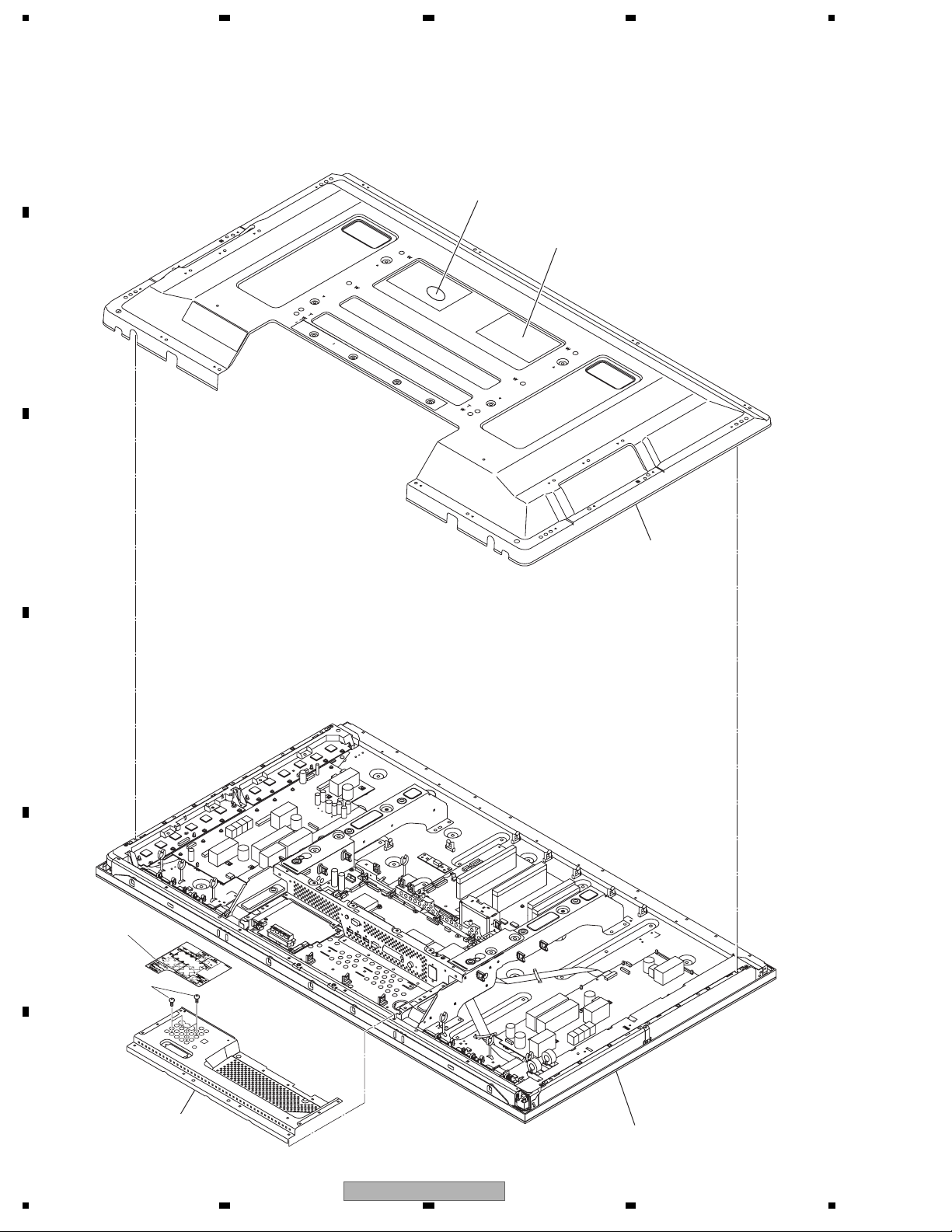
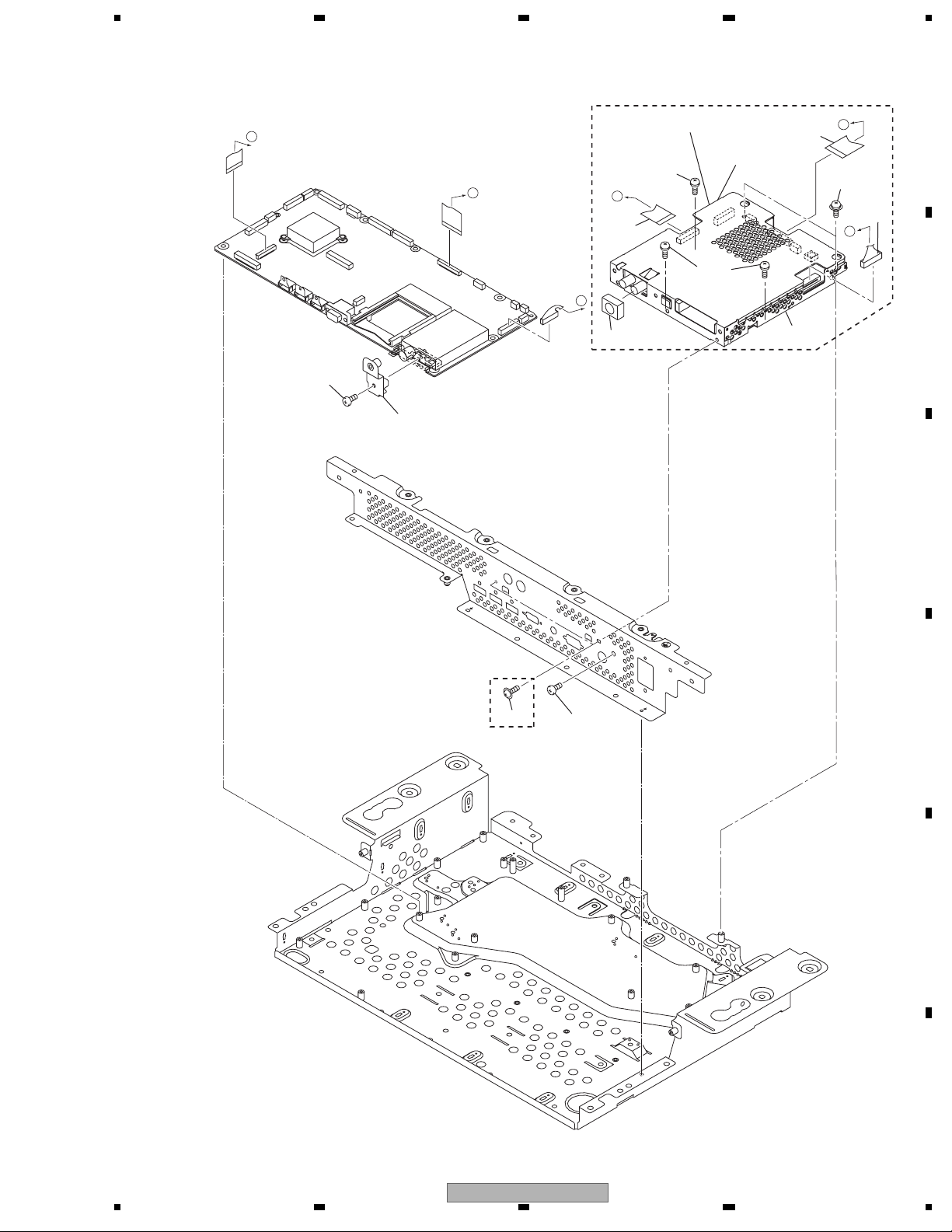
1.0.1 EXPLODED VIEWS
EXTERIOR (Rear Section)
A
B
No. 3
No. 2
C
Rear Case
D
E
Label B
No. 15
F
Terminal Panel B
Refer to
"10.3 FRONT SECTION".
6
1 234
PDP-508XG
Page 7
5678
EXTERIOR (Mult Base Section)
F
PDP-508XDA only
No. 1 DTV Tuner Board
No. 5
H
A
No. 8
No. 9
H
F
No. 6
No. 11
No. 4
G
No. 9
Screw
(ABA1354)
No. 13
No. 10
PDP-508XDA
only
G
No. 14
No. 12
B
No. 7
C
D
PDP-508XG
56
E
F
7
7
8
Page 8
1234
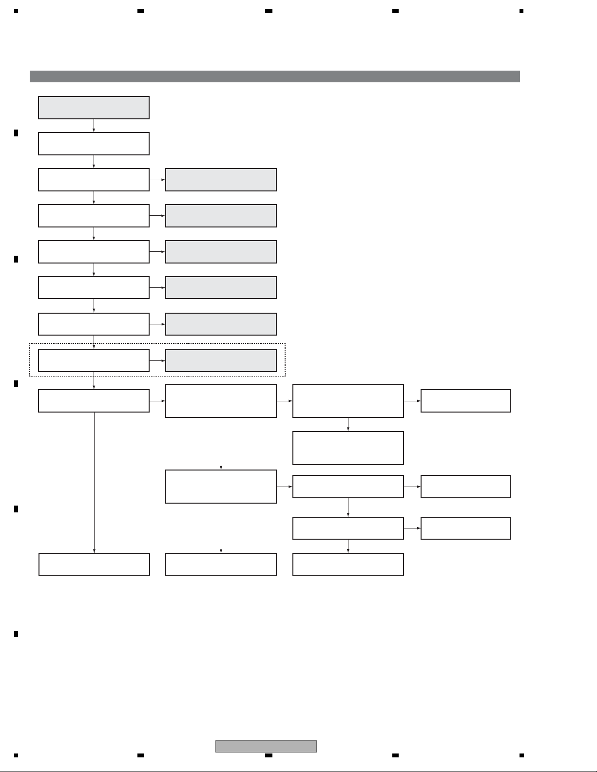
2. BASIC ITEMS FOR SERVICE
2.1 QUICK REFERENCE
A
Quick Reference upon Service Visit 1
Notes, PD/SD diagnosis, and methods for various settings
Notes when visiting for service
1. Notes when disassembling/reassembling
1 Rear case
When reassembling the rear case, the screws must be tightened in a
specific order. Be careful not to tighten them in the wrong order forcibly.
For details, see "Rear Case" in "7. DISASSEMBLY".
2 Attaching screws for the HDMI connector
When attaching the HDMI connector after replacing the Main Assy,
secure the HDMI connector manually with a screwdriver, but not
with an electric screwdriver. If you tighten the screws too tightly
with an electric screwdriver, the screw heads may be damaged, in
B
which case the screws cannot be untightened/tightened any more.
2. On parts replacement
1 How to discharge before replacing the Assys
A charge of significant voltage remains in the Plasma Panel even
after the power is turned off. Safely discharge the panel before
replacement of parts, in either manner indicated below:
Let the panel sit at least for 3 minutes after the power is turned off.
A:
B: Turn the Large Signal System off before the power is turned off
then, after 1 minute, turn the power off.
For details, see "5.6.1 PANEL DRIVE-POWER ON/OFF
FUNCTION".
2 On the settings after replacement of the Assys
Some boards need settings made after replacement of the Assys.
For details, see "8. EACH SETTING AND ADJUSTMENT".
C
3. On various settings
1 Setting in Factory mode
After a Mask indication into the panel is performed, be sure to
set the Mask setting to "OFF" then exit Factory mode.
PD/SD
Item
SQ_LSI
Communication with the module IIC
DIGITAL-RST2
Panel high temperature
Panel section
Audio/
Short-circuit SP terminal
Communication with the Module UCOM
Main 3-wire serial communication
Main IIC communication
Communication with the Main UCOM
FAN
MTB section
Unit high temperature
Digital Tuner communication
MTB-RST2/RST4
Main EEPROM
POWER
SCAN
SCN-5V
Y- D R I VE
Y-DCDC
Y- S U S
ADRS
X-DRIVE
X-DCDC
X-SUS
DIG-DCDC
UNKNOWN
No. of LEDs
flashing
Red Blue
Blue 1
Blue 2
Blue 3
Blue 4
Blue 5
Blue 6
Blue 7
Blue 8
Blue 9
Blue 10
Blue 11
Blue 12
Blue 13
Blue 15
Red 2
Red 3
Red 4
Red 5
Red 6
Red 7
Red 8
Red 9
Red 10
Red 11
Red 12
Red 15
LED Display Information
1 Rewriting software
2 PD (2-15)
3 SD (1-15)
4 No backup
This indication does not display all
LED patterns.
For details, please refer to 5.1.1 LED
DISPLAY INFORMATION.
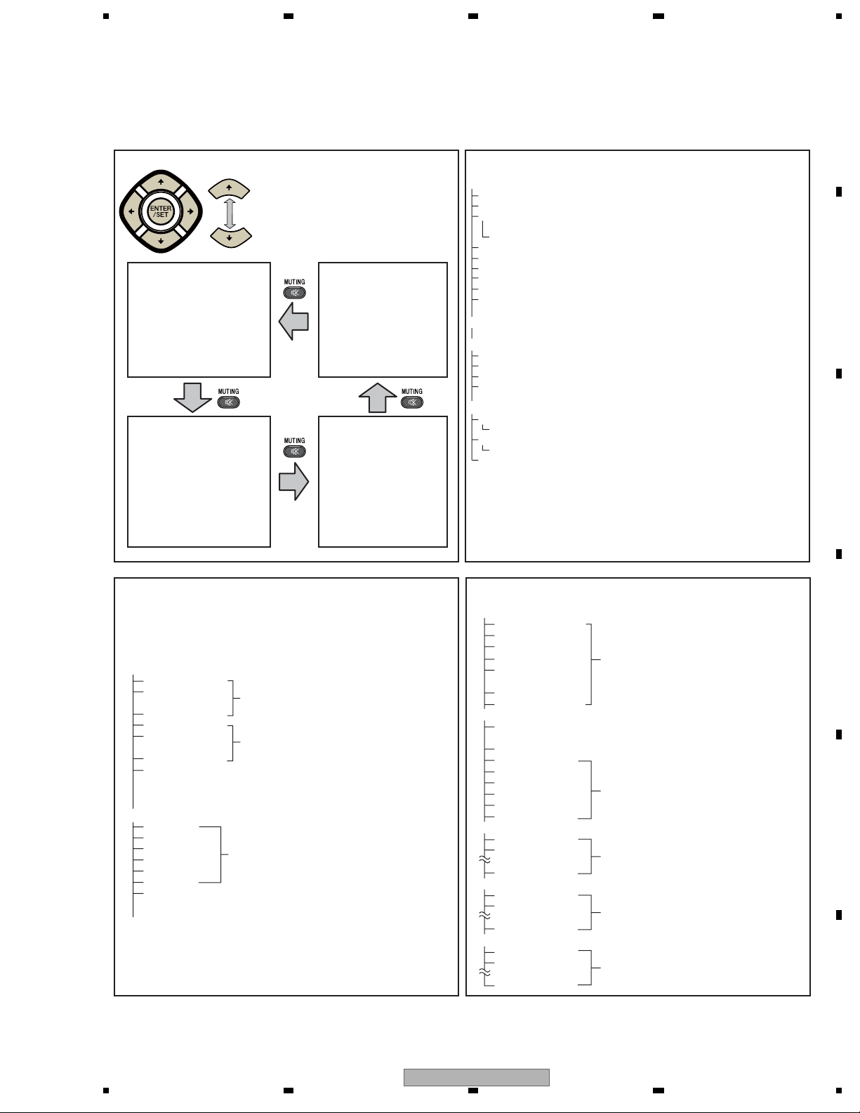
How to locate several items on the Factory menu
{ } : Item on the Factory menu
D
E
F
[ ] : Key on the remote control unit
" " : Screen indication
1. Confirmation of accumulated power-on time and power-on
count
Select {INFORMATION} then {HOUR METER}.
(After entering Factory mode, press
[j] five times.)
2. Confirmation of the Power-down and Shutdown histories
1 Panel system
PD: Select {PANEL FACTORY} then {POWER DOWN}.
(After entering Factory mode, press [MUTING] once, press
[ENTER/SET], then press
[j] three times.)
SD: Select {PANEL FACTORY} then {SHUT DOWN}.
(After entering Factory mode, press [MUTING] once, press
[ENTER/SET], then press
[j] four times.)
2 MTB section
Select {INFORMATION} then {MAIN NG}.
(After entering Factory mode, press
[j] three times.)
3. How to display the Mask indication
1 Mask indication in the panel side
1. Select {PANEL FACTORY} then {RASTER MASK SETUP}.
(After entering Factory mode, press [MUTING] once, press
[ENTER/SET], then press
2. Press [ENTER/SET], then select a Mask indication, using
[j] 8 times.)
[j] or [i].
Adjustments and Settings after replacement of the
Assys (Procedures in Factory mode)
1. Digital Video Assy: Transfer of backup data
1 Select {PANEL FACTORY}, {ETC}, then {BACKUP DATA}. (After entering Factory
mode, press [MUTING] once, press [ENTER/SET], press [j] seven times, then
press [ENTER/SET].)
2 Select {TRANSFER}, using [l], then hold [ENTER/SET] pressed for at least 5
seconds.
3 After transfer of backup data is completed, {ETC} is automatically selected, and the
LED on the front panel returns to normal lighting.
2. MAIN Assy: Execution of FINAL SETUP.
1 Select {INITIALIZE} then {FINAL SETUP}, then press [ENTER/SET]. (After entering
Factory mode, press [MUTING] three times, then press [j] four times.)
2 Select "YES", using [l]. Then hold [ENTER/SET] pressed for at least 5 seconds.
3 After "FINAL SETUP IS COMPLETE" is displayed on the screen, turn the POWER
switch of the main unit off.
3. POWER SUPPLY Unit: Clearance of the accumulated power-on count
and maximum temperature value
1 Select {PANEL FACTORY}, {ETC}, then {P COUNT INFO}. (After entering Factory
mode, press [MUTING] once, press [ENTER/SET], press [j] seven times, press
[ENTER/SET], then press [j] six times.)
2 Press [l] to select "CLEAR". Hold [ENTER/SET] pressed for at least 5 seconds.
After clearance is completed, "ETC" is automatically selected. Clear the maximum
temperature value (MAX TEMP) in the same manner.
4. Other Assys: Clearance of the maximum temperature value
1 Select {PANEL FACTORY}, {ETC}, then {MAX TEMP}. (After entering Factory mode,
press [MUTING] once, press [ENTER/SET], press [j] seven times, press
[ENTER/SET], then press [j] seven times.)
2 Press [l] to select "CLEAR". Hold [ENTER/SET] pressed for at least 5 seconds.
After clearance is completed, "ETC" is automatically selected.
8
1 234
PDP-508XG
Page 9
5678
Quick Reference upon Service Visit 2
Mode transition and structure of layers in Service Factory mode
Mode transition in Service Factory mode
INFORMATION mode
1. VERSION (1)
2. VERSION (2)
3. MAIN NG
4. TEMPERATURE
5. HOUR METER
6. HDMI SIGNAL INFO1
7. HDMI SIGNAL INFO2
8. VDEC SIGNAL INFO1
9. VDEC SIGNAL INFO2
PA NEL FACTORY mode
1. PANEL INFORMATION
2. PANEL WORKS
3. POWER DOWN
4. SHUT DOWN
5. PANEL-1 ADJ
6. PANEL-2 ADJ
7. PANEL FUNCTION
8. ETC.
9. RASTER MASK SETUP
10. PATTEN MASK SETUP
11. COMBI MASK SETUP
Up
Down
• To shift to another mode, press [MUTING].
• To shift to another item in a specific mode,
press [i] or [j].
• To shift to the next nested layer below for an
item with a "(+)" indication, press [ENTER/SET].
To return to the next nested layer above,
also press [ENTER/SET].
INITIALIZE mode
1. SIDE MASK LEVEL
2. FINAL SETUP
3. Wide XGA AUTO
OPTION mode
1. EDID WRITE MODE
2. CH PRESET
3. AFT
4. SYNC DET
Structure of Layers in Service Factory Mode
INFORMATION mode
1. VERSION (1) The software versions for each microcomputer
2. VERSION (2) The Flash memory versions for each device
3. MAIN NG The shutdown message ID/event times
(Going Clear mode by [ENTER/SET] key)
3-1. CLEAR
4. TEMPERATURE The temperature/FAN rotating status/Room light sensor
5. HOUR METER The HOUR METER/P-COUNT information
6. HDMI SIGNAL INFO 1 The information of HDMI information files
7. HDMI SIGNAL INFO 2 The information of HDMI information files
8. VDEC SIGNAL INFO 1 The signal information of VDEC
9. VDEC SIGNAL INFO 2 The signal information of VDEC
PA NEL FACTORY mode Refer to [PANEL FACTORY MODE]
OPTION mode
1. EDID WRITE MODE For factory use
2. CH PRESET For production line use
3. AFT For factory use
4. SYNC DET For technical analysis
INITIALIZE mode
1. SIDE MASK LEVEL For factory use
1-1. SIDE MASK LEVEL
2. FINAL SETUP Set to Factory default settings (it should perform after
2-1. DATA RESET replacing a MAIN Assy)
3. Wide XGA AUTO For technical analysis
Select Yes by [l] key, l pressing and hold [ENTER/SET] key
A
B
C
Structure of Layers in Panel Factory Mode 1
1. PANEL INFORMATION Version indication of the panel
2. PANEL WORKS Indications of the accumulated power-on time, pulse-meter
count, and power-on count of the panel
3. POWER DOWN Indication of the Power-down history
4. SHUT DOWN Indication of the Shutdown history
5. PANEL-1 ADJ (+)
1. VOL SUS
2. VOL OFFSET
• • • • •
8. VOL YNOFS4
9. RESET1ST_KSB
10. RESET2ND_KSB
• • • • •
23. YSTL_FMR_HZ
24. SUS FREQ
6. PANEL-2 ADJ (+)
1. R-HIGH
2. G-HIGH
3 .B-HIGH Parameters for the WB adjustment of the panel, which are
4. R-LOW required during adjustment after panel replacement
5. G-LOW
6. B-LOW
7. ABL Setting of the power consumption. A setting table is
availab
To "Structure of Layers in Panel Factory Mode 2"
Settings required after replacement of the panel
Modification not required because these items
are basically for factory presetting
For AM noise prevention (Depending on the mode,
brightness of the screen changes.)
For confirmation of the result of the setting change,
the unit must be turned off then back on again.
le for each vertical signal.
Structure of Layers in Panel Factory Mode 2
7. PANEL FUNCTION (+)
1. R-LEVEL
2. G-LEVEL
3. B-LEVEL
4. ADDRESS L1 Items for use by engineers
5. ADDRESS L2
• • • • •
11. ADDRESS U4
12. STK MODE
8. ETC (+)
1. BACKUP DATA For transferring backup data (after replacement of
the DIGITAL Assy)
2. DIGITAL EEPROM To clear data of the digital video
3. PD INFO.
4. SD INFO. For clearance of data for the corresponding items.
5. HR-MTR INFO. The clearing method is the same: Select "CLEAR",
6. PM/B1-B5 using [l], then hold [ENTER/SET] pressed for at
7. P COUNT INFO. least 5 seconds. After clearance is completed, {ETC}
8. MAX TEMP. is automatically selected.
9. RASTER MASK SETUP (+)
1. MASK OFF
2. RST MASK 01 For use while Raster Mask (full mask) is displayed.
• • • • • Use [i] or [j] to select the type of mask.
26. RST MASK 25
10. PATTEN MASK SETUP (+)
1. MASK OFF
2. PTN MASK 01 For use while Pattern Mask is displayed. Use [i] or
• • • • • [j] to select the type of mask.
50. PTN MASK 49
11. COMBI MASK SETUP (+)
1. MASK OFF
2. CMB MASK 01 For use while Combination Mask is displayed.
• • • • • Use [i] or [j] to select the type of mask.
1
8. CMB MASK 17
D
E
F
PDP-508XG
56
9
7
8
Page 10

1234
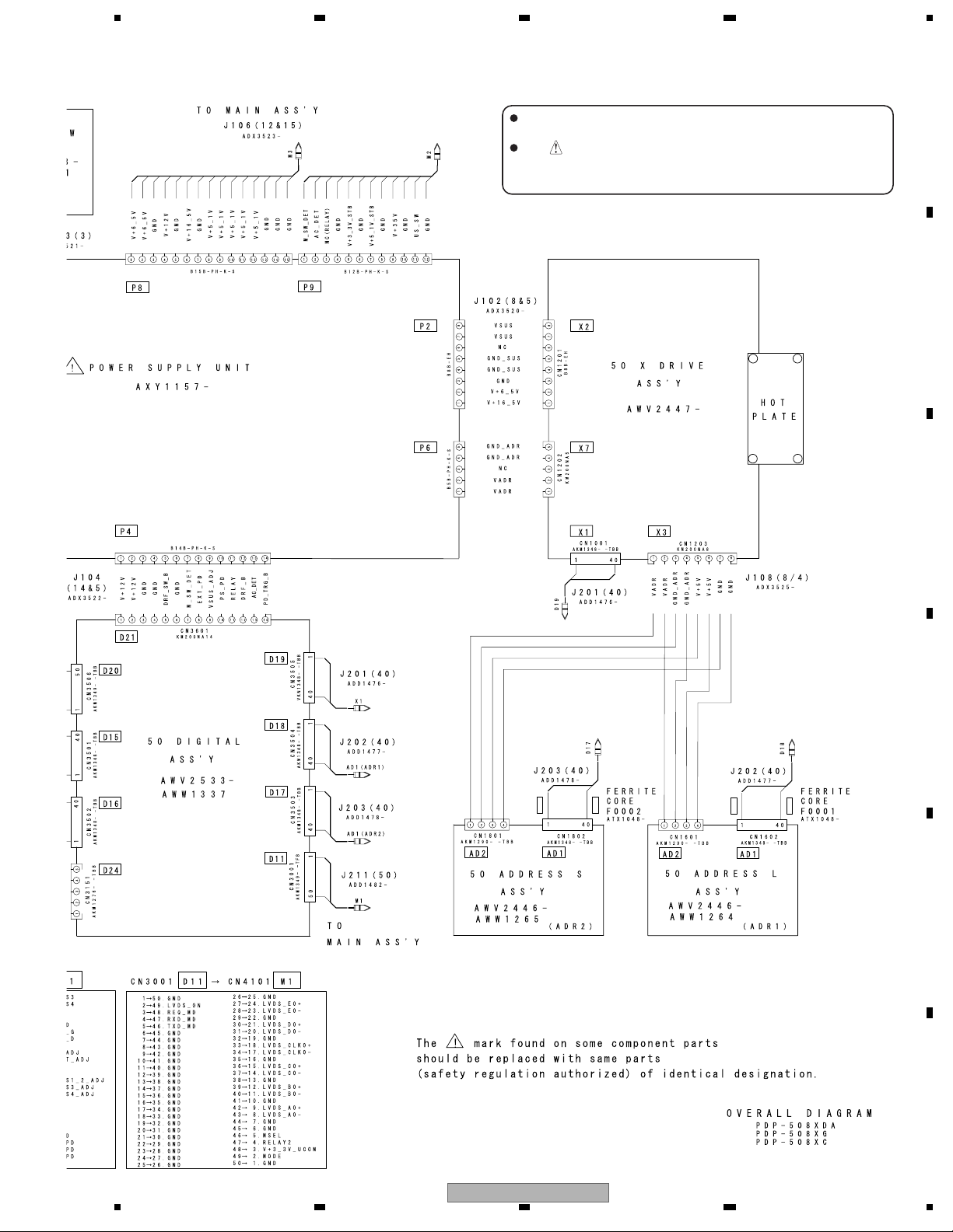
3. BLOCK DIAGRAM
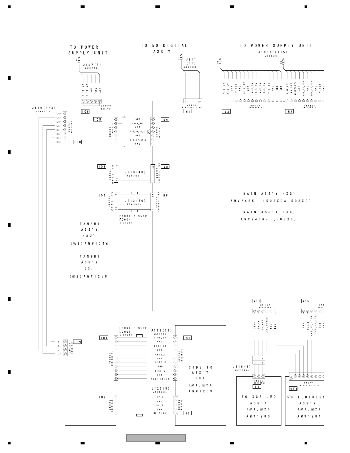
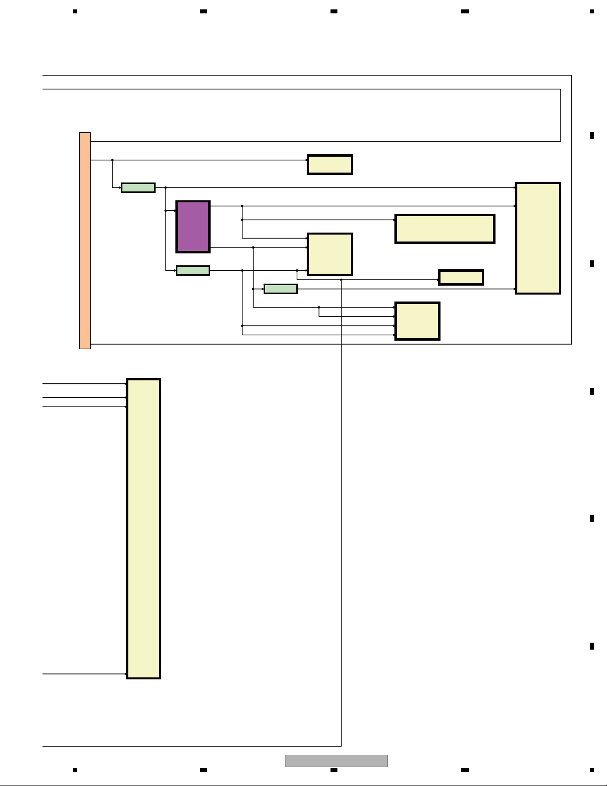
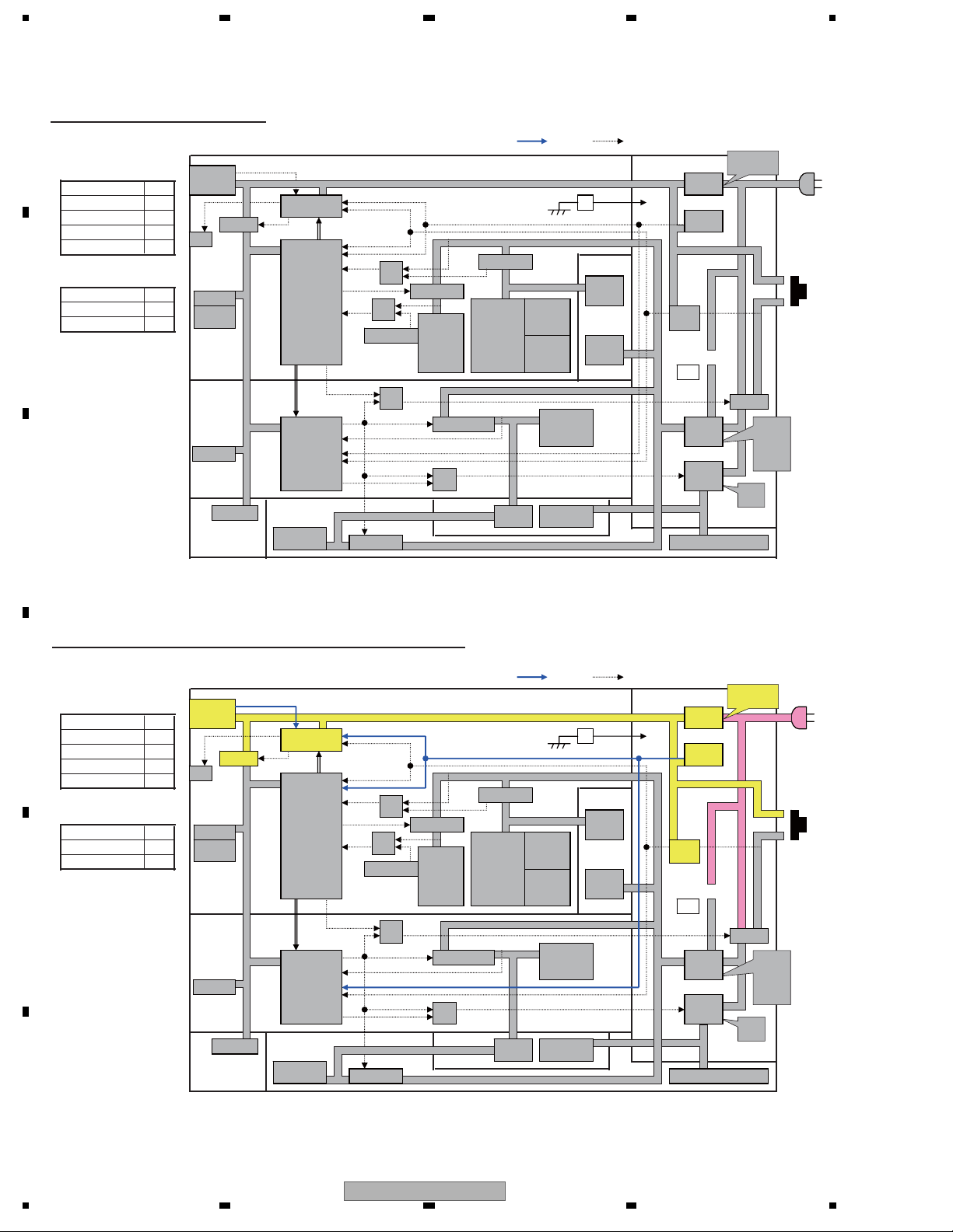
3.1 OVERALL WIRING DIAGRAM (1/2)
A
B
C
D
E
F
10
1 234
PDP-508XG
Page 11
5678
When ordering service parts, be sure to refer to "EXPLODED
VIEWS and PARTS LIST" or "PCB PARTS LIST".
The mark found on some component parts indicates the
importance of the safety factor of the part. Therefore, when
replacing, be sure to use parts of identical designation.
A
B
C
D
E
F
PDP-508XG
56
11
7
8
Page 12
1234
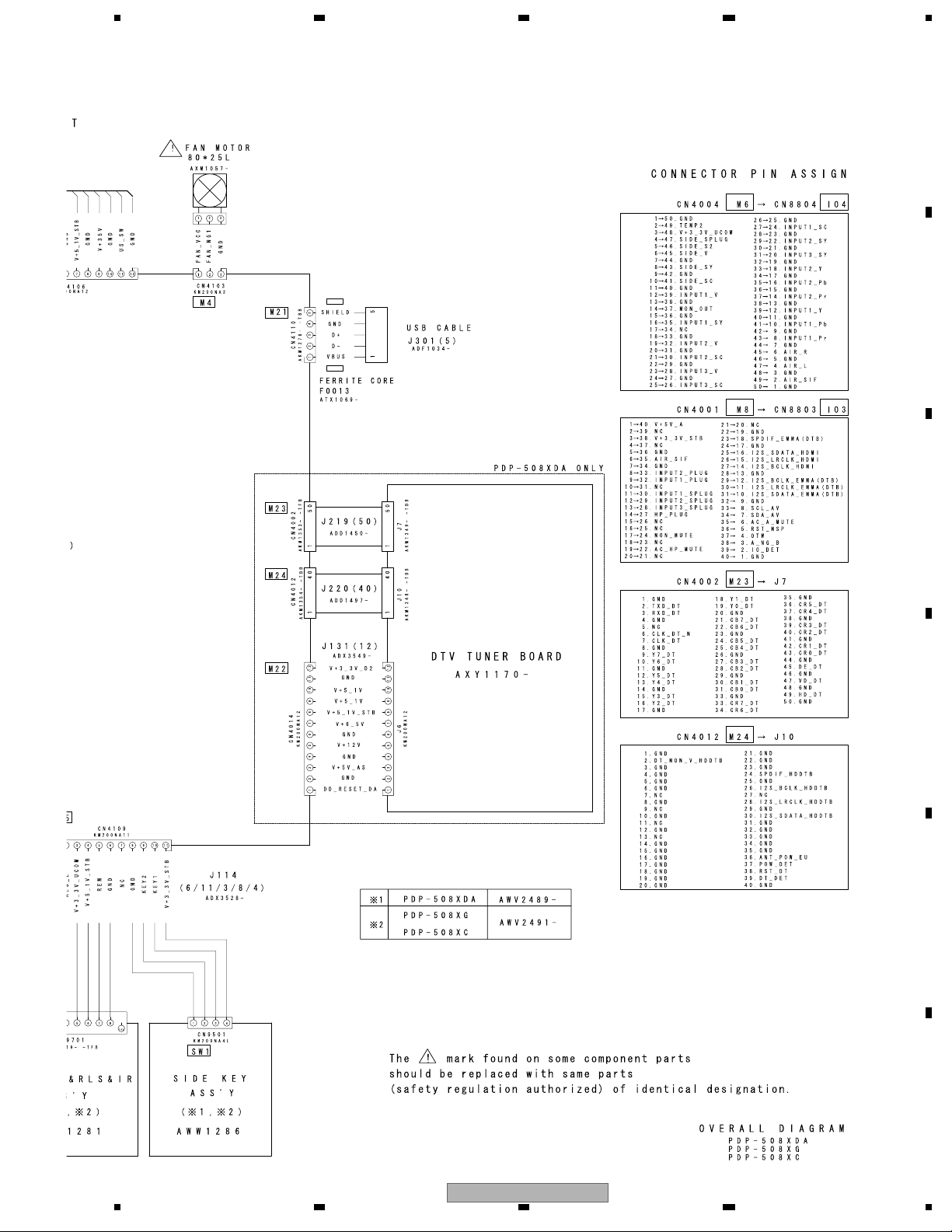
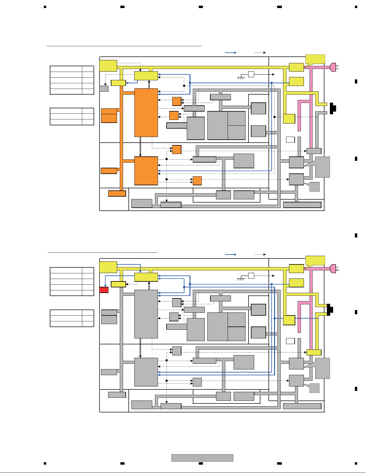
3.2 OVERALL WIRING DIAGRAM (2/2)
A
B
C
D
E
F
12
1 234
PDP-508XG
Page 13
5678
A
B
C
D
E
PDP-508XG
56
F
13
7
8
Page 14
1234
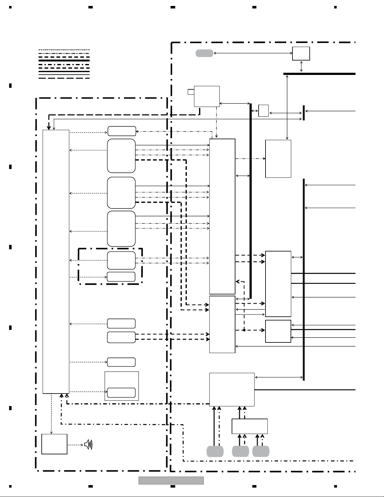
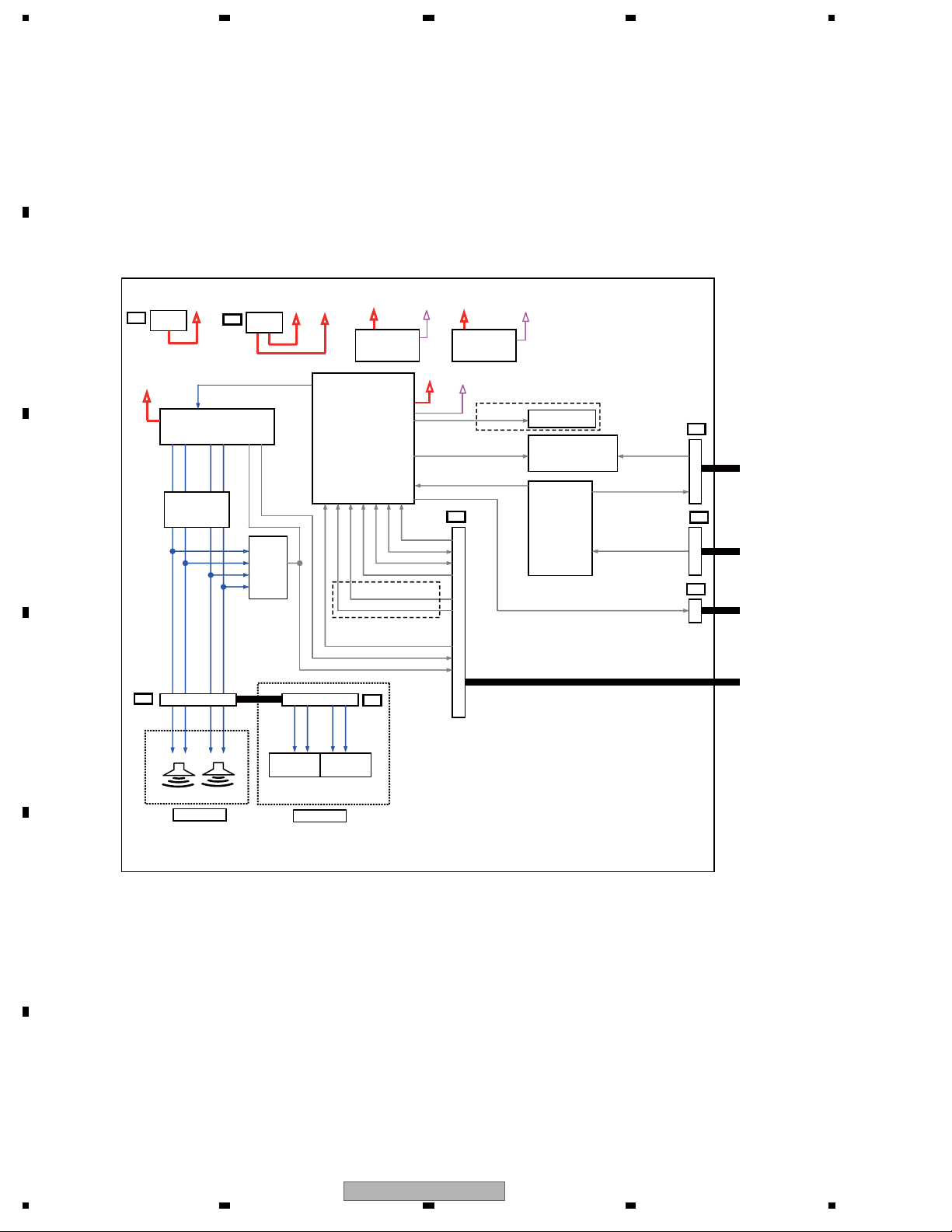
3.3 OVERALL BLOCK DIAGRAM
A
Analogue SIF
SCL_AV
B
SDA_AV
Analog Audio signal
Analog Video signal
Component signal
Digital Video signal
Digital Audio signal
Synchronized signal
Data signal
Control signal
RF signal
MON_OUT_L/R
L/R IN
L/R IN
JA8901
Monitor Out
JA8901
Input1
JA8901
Input2
MON_OUT_V
SPLUG
CVBS
Y/C
SPLUG
CVBS
Y/C
USB
U6001
AXF1180
(Tuner)
VIDEO
IC6401
M65596FP
(USB)
Add1-6
Data0-15
Add0-3
Data0-7
TSSI[0:10]
SCL_AV5
SDA_AV5
Analogue
CVBS
SCL_AV5
SDA_AV5
Q8405
SSM6N
17FU
SCL_AV
SDA_AV
IC6301
TC90173FG
(VBI)
SCL_AV
SDA_AV
C
IC4601
R2S11006FT
(AVSW)
Y/C
L/R IN
JA8901
Input3
SPLUG
CVBS
SIDE IO
IC9101
MSP5651M
(MSP)
ASSY
L/R IN
JA9351
JA9352
Input6
Y/C
CVBS
Main
Sub
SCL_MB
SDA_MB
HP_L/R OUT
D
PC_L/R IN
CN9353
Head Phone
JA9001
Audio Input for PC
CN4701
PC Input
Y/Pb/Pr
Y/Pb/Pr
PC_RGB
PC_H/V
IC4701
R2S11001FT
(RGBSW)
Y
RGB
CLP
FB
RGB/YPbPr
IC4801
CM0048BF
(VDEC)
IC5001
AD9985KSTZ
(ADC)
CLP
SW_L/R OUT
JA8901
SUB WOOFER
E
PDP-428XDA
PDP-508XDA
OPT_OUT
JA9081
SPDIF
SPDIF
I2S,SPDIF
IC9201
TAS5122DCA
ONLY
F
(D-AMP)
INPUT3
HDMI
IC5201
SII9125CTU
(HDMI RX)
INPUT4
HDMI
IC5101
CXB1442
(HDMI SW)
INPUT5
HDMI
MAIN ASSY
TANSHI ASSY
14
PDP-508XG
1 234
Page 15
5678
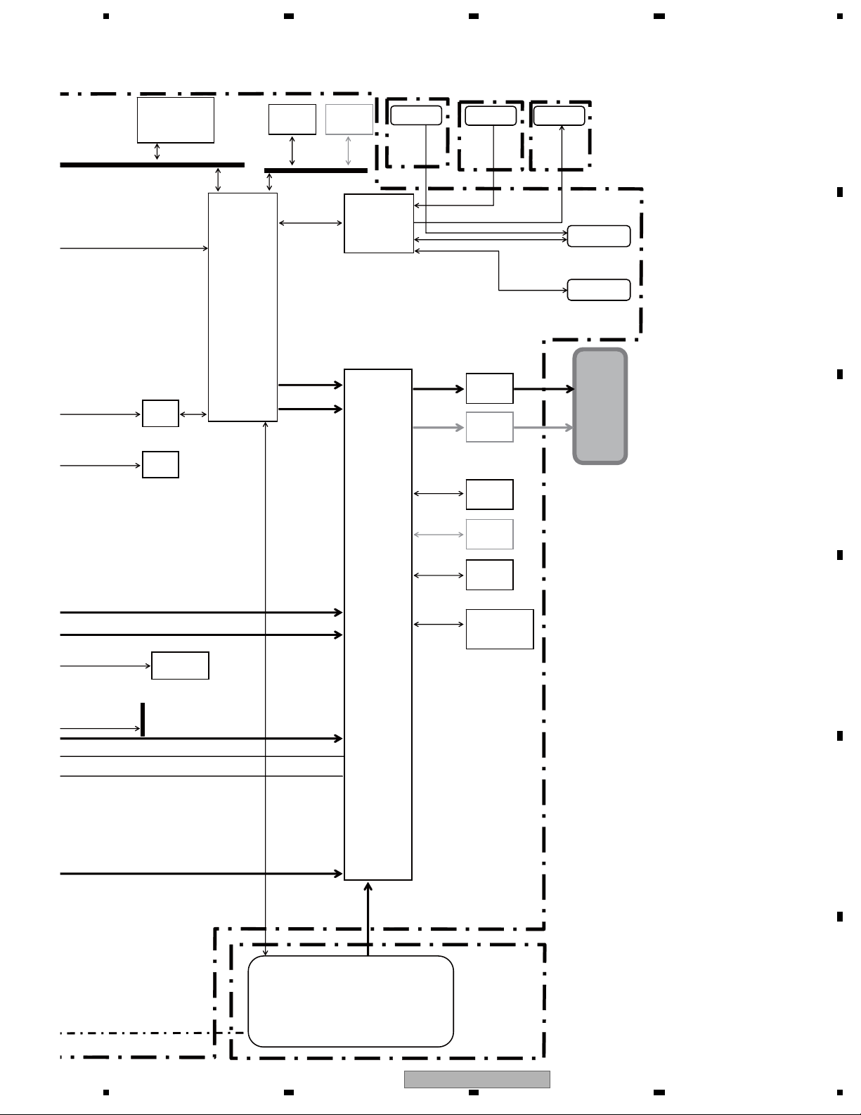
SCL_MB
SDA_MB
IC8602
XGA:AGC1042
FHD:AGC1047
(S29GL032A90TFIR4-K)
32Mbit Flash
Add1-17
Data0-15
ROM IF
I2C-1
IC8407
6
IC8404
BR24F64F
(EEPROM)
I2C-0
TC74HC406
IC8401
uPD61123F1
II
(EMMA
SV)
IC8601
K4H511638D
512Mbit DDR
UMI
TXD_DT
RXD_DT
Add0-12
Data0-15
OSD 8bit *4
FHD
IC8605
K4H510838D
512Mbit DDR
Add0-12
Data0-7
(M30620FCSGP-U5-K)
50LED&RLS
&IR ASSY
IR
REM
IC8301
AGC1037
IF UCOM
SIDE KEY
ASSY
KEY
KEY_AD1
KEY_AD2
IC4101
BU8254KVT
(LVDS)
IC4102
BU8254KVT
(LVDS)
IC8201
EDD1232ABBH
128Mbit (DDR)
50XGA LED
ASSY
LED
SR_OUT
TXD_SR
RXD_SR
232C_CH2
232C_CH3
232C_CH4
232C_CH8
FHD
SR_OUT
RS232C
To
Digital
Ass'y
A
B
C
SCL_AV
SDA_AV
CLP
IC4802
HY57V161610FTP
16Mbit(SDRAM)
TXD_DT
RXD_DT
656 10bit
656 8bit
8bit *3
12bit *3
IC8001
PD6568A
(ARIA)
8bit*3
IC8202
EDD1232ABBH
128Mbit (DDR)
EDD1232ABBH
128Mbit (DDR)
(S29GL016A90TFIR2-K)
IC8203
IC8204
AGC1050
16Mbit Flash
FHD
D
E
PDP-428XDA
PDP-508XDA
DTV TUNER BOARD
ONLY
I2S
PDP-508XG
56
F
15
7
8
Page 16

1234
DDC
BD8602FV-TBB
FET SW
RTQ040P02-TLB
5V Reg
PQ200WNA1ZPH-TLB
5V Reg
NJM2846DL3-05-TLB
5V Reg
NJM2846DL3-05-TLB
1.8V Reg
NJM2846DL3-18-TLB
FAN VCC Reg
PQ200WNA1ZPH-TLB
3.3V Reg
NJM2846DL3-33-TLB
USB CONNECTOR
SW
R5523N001B-TLB
FRONT END
AXF1180-
AV SW
R2S11006FT-K
FAN
FET SW
RTQ040P02-TLB
ADC
AD9985KSTZ-110-K
FET SW
RTQ045N03-TLB
VDEC SDRAM
HY57V161610FTP-7-K
1.8V Reg
NJM2846DL3-18-TLB
HDMI SW
CXB1442R-K
HDMI Rx
SII9125CTU-K
FET SW
MCH3406-TLB
LVDS Tx
BU8254KVT-K
ARIA
UPD61123F1100KA3A-K
ARIA ROM
AGC1050-A-PI-K
(S29GL016A90TFIR2K)
FET SW
UPA1917TE-TRB
MSP
MSP5651M-QK-C2-K
RGB SW
R2S11001FT-K
FPF2007-TLB
2SC4081(QR)-TLB
DDR SDRAM
EDD1232ABBH-5C-E-
DDR SDRAM
EDD1232ABBH-5C-E-
8V Reg
PQ200WNA1ZPH-TLB
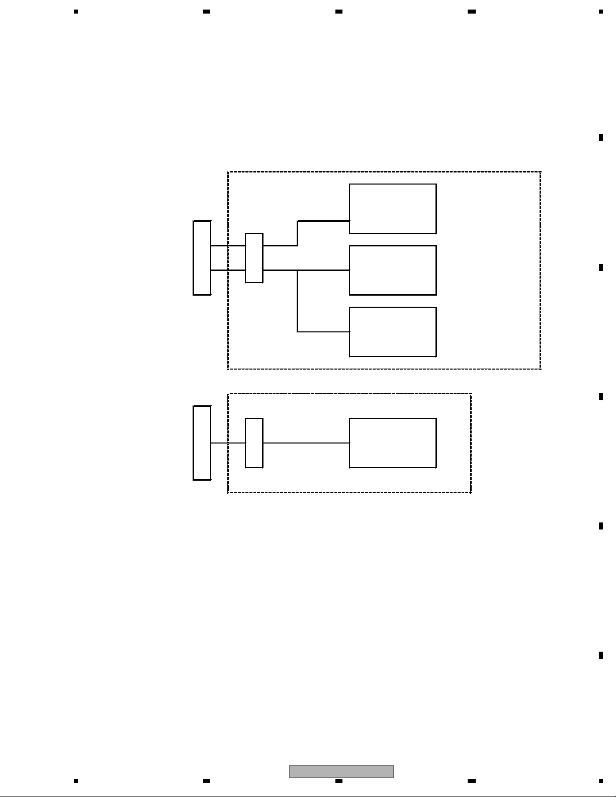
3.4 POWER SUPPLY BLOCK of MULTI BASE SECTION
CN4105
V+6_5V
A
V+12V
B
C
IC4305
V+5_1V
IC4309
IC4403
IC4307
IC4301
IC4310
V+5V_USB
V+5V_ANT
V+3_3V_D
V+5V_A
V+8V_A
FAN_VCC
Q4415
IC6403
V+3_3V_D2
USB1_VBUS
V+5V_A2 V+5V_A2_RGB
V+5V_A_AV
V+8V_A_AV
V+3_3V_D2_VDEC_SDRAM
Q4418
V+3_3V_D3
IC4802
V+3_3V_D3_HDMI
IC4404
IC4601
TANSHI Assy
V+3_3V_AU_D
V+3_3V_D3_HDMI_A
V+3_3V_D3_HDMI_IO
V+3_3V_D3_HDMI_REG
V+3_3V_D3_HDMISW
V+1_8V_A
U6001
IC9191
IC5101
V+1_8V_A_HDMI
ANT_POW_TU
V+31_5V
IC4701
V+3_3V_AU_A
V+1_8V_A_HDMI_A
V+1_8V_A_HDMI_C
V+1_8V_A_HDMI_D
V+8V_AU
V+1_8V_AU
IC4410
Q4306
IC9101
IC5201
D
E
F
IC4401
Q4404
V+1_2V_D V+1_2V_D_ARIA
V+2_5V_D
V+2_5V_D_ARIA
V+3_3V_A__AD V+3_3V_A__AD_A
V+3_3V_A
Q4409
V+3_3V_D4 V+3_3V_D4_LVDS
V+3_3V_A_VDEC
V+3_3V_D4_LVDS_OUT
V+3_3V_D4_LVDS_PLL_A
+3_3V_D4_LVDS_LVDS
V
V+3_3V_D4_ARIA_ROM
V+3_3V_D4_ARIA
V+1_2V_D_ARIA_PLL1
V+1_2V_D_ARIA_PLL2
V+1_2V_D_ARIA_PLL3
V+1_2V_D_ARIA_PLL4
V+VDDIO_ARIA
V+VDDIO_ARIA_DDR_A
V+VDDIO_ARIA_DDR_C
IC4101
IC8204
IC8203
Q4422
IC8401
IC8201
V+1_8V_A_VDEC
V+3_3V_D_AD_D
V+3_3V_A__AD_PLL
PDP-428XDA,PDP-508XDA Only
V+5_1V
V+12V
V+6_5V
V+3_3V_UCOM
IC5001
C
N4014
16
PDP-508XG
1 234
Page 17
CN4106
IF UCOM
AGC1037- -PI-K
(M30620FCSGP-U5-K)
VDEC
CM0048BF-K
FET SW
RSS090P03-TBB
DDC
LTC3407EMSE-
2-TBB
VBI SLICER
TC90173FG-K
EMMA2
UPD61123F1100KA3A-K
DDR DRAM
1:K4H511638D-UCB3-K
2:EDD5116AFTA-6B-E-K
3:HY5DU121622CTP-J
FET SW
MCH3406-TLB
USB CONROLLER
M66596FP-K
FET SW
RTQ040P02-TLB
EMMA2 FLASH ROM
AGC1042- -PI-K
(S29GL032A90TFIR4-
V+35V
V+3_3V_STB
5678
A
IC8301
V+5_1V_STB
V+1_8V_A_VDEC_D
V+1_8V_A_VDEC_PLL
V+3_3V_D2_VDEC_D
Q4512
IC4801
V+3_3V_ACT
IC4501
Q4511
V+2_5V_UCOM
V+1_5V_UCOM
V+3_3V_UCOM_USB
V+3_3V_UCOM_VBI
V+2_5V_UCOM2 V+2_5V_UCOM_VBI
V+2_5V_UCOM_DDR
V+2_5V_EMMA
V+1_5V_UCOM_EMMA
V+3_3V_UCOM
Q4505
V+1_5V_UCOM_USB V+1_5V_UCOM_USB_D
IC8401
V+1_5V_UCOM2
V+1_5V_UCOM_USB_A
V+3_3V_UCOM_USB_D
V+3_3V_UCOM_USB_A
IC8601
V+3_3V_UCOM_ROM
IC6401
IC8602
V+1_5V_UCOM_VBI
IC6301
B
C
D
V+3_3V_A_VDEC_A
PDP-508XG
56
E
F
17
7
8
Page 18
1234
for MAIN ASSY
DIGITAL AMP IC
IC9201
TAS5122DCA
MSP IC
IC9101
MSP5651M
IO3
INPUT1
INPUT2
INPUT3
INPUT6
PC AUDIO
SUB WOOFER OUT
MONITOR OUT
LPF
IO9
IO4
IO1
IO2
OUTPUT(VIDEO)
3.5 TANSHI ASSY
A
TANSHI ASSY XGA BLOCK DIAGRAM
B
IO6
+16.5V
+16.5V
IO5
PWM
+8V
+3.3V
+16.5V
REGULATOR
IC9181
NJM78M12DL1A
+3.3V
+12V
REGULATOR
IC9191
NJM2846DL3
+3.3V
+1.8V
OUTPUT(AUDIO)
INPUT(AUDIO)
+1.8V
*PDP-428XDA,PDP-508XDA only
OPT_OUT
OPTICAL OUT
INPUT(VIDEO)
C
IO8
R_OUT+
R_OUT-
L_OUT+
L_OUT-
DC
DETECT
BLOCK
RST_MSP
I2S_EMMA
SPDIF_EMMA
*PDP-508XDA,PDP-428XDA only
SPDIF_HDMI
OTW
A_NG_B
SDA
AIR_SIF
SCL
HP
INPUT6
for SIDE IO ASSY
for SIDE IO ASSY
for MAIN ASSY
D
E
F
18
R OUT
L OUT
SP TERMINAL
42inch only
50inch only
TANSHI ASS'Y
PDP-508XG
1 234
Page 19
5678
RLS
IC9704
AMS114YD01
OP AMP
IC9703
MM3012XN
MAIN ASSY
CN9501
KEY
S9501 to S9506
MAIN ASSY
CN9701
IR
IC9702
SBX3050-01
3.6 POWER SUPPLY BLOCK of 50LED&IR&RLS and SIDE KEY ASSYS
50LED&IR&RLS ASSY
V+5_1V_STB
V+3_3V_UCOM
A
B
KEY ASSY
V+3_3V_STB
C
D
E
PDP-508XG
56
F
19
7
8
Page 20
1234
4. DIAGNOSIS
DIAGNOSIS of PDP-508XG/DLFT,PDP-508XDA/YP and PDP-508XC/WA5 is the same as PDP-5080XA/WYV5 except for the following:
4.1 POWER SUPPLY OPERATION
4.1.1 LED DISPLAY INFORMATION
A
LED Pattern
POWER ON STANDBY SLEEP
State
AC OFF or Main
power switch OFF
B
Standby power
management
Power ON
(Screen ON)
Power-down
Shutdown
C
No digital adjustment
data copied for
backup
In the process of
rewriting the program
of the microcomputer
During factory
operation
Sleep timer
D
LED Pattern Remarks
B
R
O
B
R
O
B
R
O
B Once Twice n times 2.5s Once
R 500ms
O
B 500ms
R Once Twice n times 2.5s Once
O
B 200ms
R
O
B 100ms
R 100ms
O
B
R
O
B
R
O
The LEDs flash only while the
panel is turned on.
E
F
20
1 234
PDP-508XG
Page 21

5678
4.1.2 POWER ON SEQUENCE
A
REM
infrared
receiver
Inv. Amp
Q9731
Inv. Amp
Q8302
REM
Inv. Amp
Q4105
SR_OUT
SR_IN
Microcomputer
1
Side Keys
1
IF
IC8301
KEY_1
KEY_2
TXD_IF
RXD_IF
CE_IF
REQ_IF
BUSY_IF
Microcomputer
TXD_MD
RXD_MD
REQ_MD
2
MOD
IC3151
3
MAIN
Microcomputer
IC8401
OR
RELAY2
Power MOD
4
RELAY Control
B
C
SR OUT Jack
JA9404
: The remote control (or KEY) signal is input to the IF microcomputer.
: The IF microcomputer sends the operation data of the remote control unit (or KEY) to the main microcomputer.
: The main microcomputer issues a startup command (PON) to the MOD microcomputer.
: The relay is controlled with logical OR interpretation of control signals by the main microcomputer and module
(MOD) microcomputer.
D
E
F
PDP-508XG
56
21
7
8
Page 22
1234
4.1.3 DETAILS OF POWER ON SEQUENCE
A
Power supply status - AC off
Microcomputer
B
C
output port state
IF: ACTIVE
Main: RELAY2
Main: PSW1
Module: RELAY
Module: DRF_B
Microcomputer
input port state
Main: RST4
Main: RST2
Module: RST2
IR/Key/
OFF
232C
OFF
OFF
OFF
OFF
OFF
OFF
OFF
LED
EEPROM
VBI/
USB
SW
ACTIVE
Main
EEPROM
Digital
BAK_EEP
X/Y Drive
Scan
Sensor
The state of AC cord is pulled out.
IF ucom
Main_
ucom
Module_
ucom
DRIVE
AC_DET
M_SW_DET
M_SW_DET_B
RST3
RST4
PSW1
RST2
RELAY2
DCDC/REG
AND
AND
EMG_USB
OR
RELAY
DRF_B
DCDC/REG
VDEC
HDMI
ASIC
LVDS-Tx
DCDC/REG
AND
Address
PDET
A.TUNER
A.D.TUNER
A.TUNER
D.TUNER
A.TUNER
D.TUNER
AAC-DEC
USB(Reg.)
ON OFF
DCDC/REG
AV-SW
ASIC
FAN
RGB-SW
AD
VBI
VBI
BCM
BCM
(XDA)
POD
iLink
RST2
LVDS-Rx
DAC
SQ ASIC
ADDRESS
R
I/O
US_SW
MAP
MAP
MSP
D-AMP
Power supply
STB
AC_
DET
M_SW
_DET
Jumper
P11
Vcc
Vsus
Vadr
DRIVE/SCAN
V+3.3V_STB
V+5.1V_STB
Relay
V+35V
V+16.5V
V+12V
V+6.5V
V+5.1V
VSUS
VADR
Main
Switch
AC
Power supply status - Passive standby (Main switch off)
Microcomputer
D
E
F
output port state
IF: ACTIVE
Main: RELAY2
Main: PSW1
Module: RELAY
Module: DRF_B
Microcomputer
input port state
Main: RST4
Main: RST2
Module: RST2
IR/Key/
OFF
OFF
OFF
OFF
OFF
OFF
OFF
OFF
232C
LED
EEPROM
VBI/
USB
Main
EEPROM
Digital
Sensor
SW
BAK_EEP
IF ucom
ACTIVE
Module_
X/Y Drive
Scan
DRIVE
Main_
ucom
ucom
"kill me"
M_SW_DET_B
PSW1
RST2
RELAY2
AC_DET
M_SW_DET
RST3
RST4
AND
EMG_USB
RELAY
DCDC/REG
AND
OR
DRF_B
The user operation is invalid. (All LED: OFF)
Among standby power devices, only the IF microcomputer periphery operates.
DCDC/REG
VDEC
HDMI
ASIC
LVDS-Tx
DCDC/REG
AND
Address
PDET
A.TUNER
A.D.TUNER
A.TUNER
D.TUNER
A.TUNER
D.TUNER
AAC-DEC
USB(Reg.)
ON OFF
DCDC/REG
AV-SW
VBI
VBI
BCM
BCM
(XDA)
POD
iLink
RST2
FAN
RGB-SW
AD
LVDS-Rx
DAC
SQ ASIC
ADDRESSASIC
R
I/O
US_SW
MAP
MAP
MSP
D-AMP
Power supply
M_SW
_DET
Jumper
P11
Vsus
Vadr
DRIVE/SCAN
STB
AC_
DET
Vcc
V+3.3V_STB
V+5.1V_STB
Relay
V+35V
V+16.5V
V+12V
V+6.5V
V+5.1V
VSUS
VADR
AC
Main
Switch
22
PDP-508XG
1 234
Page 23
5678
Power supply status - Active standby (Main switch off)
Microcomputer
output port state
IF: ACTIVE
Main: RELAY2
Main: PSW1
Module: RELAY
Module: DRF_B
Microcomputer
input port state
Main: RST4
Main: RST2
Module: RST2
IR/Key/
ON
OFF
OFF
OFF
OFF
OFF
OFF
OFF
232C
LED
EEPROM
VBI/
USB
Main
EEPROM
Digital
Sensor
SW
BAK_EEP
IF ucom
ACTIVE
Module_
X/Y Drive
Scan
DRIVE
Main_
ucom
ucom
AC_DET
M_SW_DET
M_SW_DET_B
RST3
RST4
PSW1
RST2
RELAY2
DCDC/REG
AND
AND
EMG_USB
OR
RELAY
DRF_B
DCDC/REG
VDEC
HDMI
ASIC
LVDS-Tx
AND
Address
The user operation is invalid. (All LED: OFF)
Standby power devices (periphery of IF/Main/Module microcomputer) operate.
PDET
DCDC/REG
ON OFF
DCDC/REG
A.TUNER
A.D.TUNER
D.TUNER
A.TUNER
A.TUNER
VBI
VBI
D.TUNER
BCM
BCM
(XDA)
POD
iLink
AAC-DEC
USB(Reg.)
RST2
AV-SW
FAN
RGB-SW
AD
LVDS-Rx
SQ ASIC
ADDRESSASIC
DAC
R
I/O
US_SW
MAP
MAP
MSP
D-AMP
Power supply
STB
AC_
DET
M_SW
_DET
Jumper
P11
Vcc
Vsus
Vadr
DRIVE/SCAN
V+3.3V_STB
V+5.1V_STB
Relay
V+35V
V+16.5V
V+12V
V+6.5V
V+5.1V
VSUS
VADR
AC
Main
Switch
A
B
C
Power supply status - Passive standby
Microcomputer
output port state
IF: ACTIVE
Main: RELAY2
Main: PSW1
Module: RELAY
Module: DRF_B
Microcomputer
input port state
Main: RST4
Main: RST2
Module: RST2
IR/Key/
OFF
OFF
OFF
OFF
OFF
OFF
OFF
OFF
232C
LED
EEPROM
VBI/
USB
SW
ACTIVE
IF ucom
Main_
ucom
"kill me"
Main
EEPROM
Module_
ucom
Digital
BAK_EEP
Sensor
X/Y Drive
Scan
DRIVE
Remote control unit waiting state. (Red LED: ON)
Among standby power devices, only the IF microcomputer periphery operates.
AC_DET
M_SW_DET
M_SW_DET_B
RST3
RST4
PSW1
RST2
RELAY2
DCDC/REG
AND
AND
EMG_USB
OR
RELAY
DRF_B
DCDC/REG
VDEC
HDMI
ASIC
LVDS-Tx
DCDC/REG
AND
Address
PDET
A.D.TUNER
A.TUNER
D.TUNER
USB(Reg.)
ON OFF
DCDC/REG
A.TUNER
D.TUNER
A.TUNER
(XDA)
iLink
AAC-DEC
RST2
VBI
VBI
BCM
BCM
POD
AV-SW
RGB-SW
ASIC
FAN
AD
LVDS-Rx
SQ ASIC
ADDRESS
DAC
R
I/O
US_SW
MAP
MAP
MSP
D-AMP
Power supply
M_SW
_DET
Jumper
P11
V+3.3V_STB
V+5.1V_STB
STB
AC_
DET
Vcc
Vsus
Vadr
DRIVE/SCAN
Relay
VSUS
VADR
V+35V
V+16.5V
V+12V
V+6.5V
V+5.1V
AC
Main
Switch
D
E
F
PDP-508XG
56
23
7
8
Page 24
1234
A
Power supply status - Active standby
Microcomputer
output port state
IF: ACTIVE
Main: RELAY2
Main: PSW1
Module: RELAY
Module: DRF_B
ON
OFF
OFF
OFF
OFF
IR/Key/
232C
LED
SW
Microcomputer
input port state
Main: RST4
Main: RST2
B
Module: RST2
OFF
OFF
OFF
EEPROM
VBI/
USB
Main
EEPROM
Digital
C
BAK_EEP
Sensor
Remote control unit waiting state. (Red LED: ON)
Standby power devices (periphery of IF/Main/Module microcomputer) operate.
IF ucom
ACTIVE
Main_
ucom
"POF"
Module_
ucom
X/Y Drive
Scan
DRIVE
AC_DET
M_SW_DET
M_SW_DET_B
RST3
RST4
PSW1
RST2
RELAY2
DCDC/REG
AND
AND
EMG_USB
OR
RELAY
DRF_B
DCDC/REG
VDEC
HDMI
ASIC
LVDS-Tx
DCDC/REG
AND
Address
PDET
A.TUNER
A.D.TUNER
A.TUNER
D.TUNER
A.TUNER
D.TUNER
AAC-DEC
USB(Reg.)
ON OFF
DCDC/REG
AV-SW
VBI
VBI
BCM
BCM
(XDA)
POD
iLink
RST2
FAN
RGB-SW
AD
LVDS-Rx
DAC
SQ ASIC
ADDRESSASIC
R
I/O
US_SW
MAP
MAP
MSP
D-AMP
Power supply
M_SW
_DET
Jumper
P11
V+3.3V_STB
V+5.1V_STB
STB
AC_
DET
Vcc
Vsus
Vadr
DRIVE/SCAN
Relay
VSUS
VADR
Power
V+35V
V+16.5V
V+12V
V+6.5V
V+5.1V
AC
Main
Switch
Power supply status - Functional standby
Microcomputer
D
E
F
output port state
IF: ACTIVE
Main: RELAY2
Main: PSW1
Module: RELAY
Module: DRF_B
Microcomputer
input port state
Main: RST4
Main: RST2
Module: RST2
IR/Key/
ON
232C
ON
OFF
OFF
OFF
ON
OFF
OFF
LED
EEPROM
VBI/
USB
SW
ACTIVE
Main
EEPROM
Digital
BAK_EEP
X/Y Drive
Scan
Sensor
Remote control unit waiting state. (Red LED: ON)
Standby power device and some Vcc power devices operate.
RGB-SW/AD/D-AMP are electrified, but uses the power-saving mode function of the IC.
IF ucom
Main_
ucom
"POF"
Module_
DRIVE
ucom
AC_DET
M_SW_DET
M_SW_DET_B
RST3
RST4
PSW1
RST2
EMG_USB
RELAY2
RELAY
DCDC/REG
AND
AND
OR
DRF_B
DCDC/REG
VDEC
HDMI
ASIC
LVDS-Tx
DCDC/REG
AND
Address
PDET
DCDC/REG
A.TUNER
A.D.TUNER
A.TUNER
D.TUNER
A.TUNER
D.TUNER
iLink
AAC-DEC
USB(Reg.)
RST2
ON OFF
AV-SW
VBI
VBI
BCM
BCM
(XDA)
POD
FAN
RGB-SW
AD
LVDS-Rx
SQ ASIC
ADDRESSASIC
DAC
R
I/O
D-AMP
US_SW
MAP
MAP
MSP
Power supply
STB
AC_
DET
M_SW
_DET
Jumper
P11
Vcc
Vsus
Vadr
DRIVE/SCAN
V+3.3V_STB
V+5.1V_STB
Relay
V+35V
V+16.5V
V+12V
V+6.5V
V+5.1V
VSUS
VADR
AC
Main
Switch
24
PDP-508XG
1 234
Page 25
5678
Power supply status - ON
Microcomputer
output port state
IF: ACTIVE ON
Main: RELAY2
Main: PSW1
Module: RELAY
Module: DRF_B
Microcomputer
input port state
Main: RST4
Main: RST2
Module: RST2
IR/Key/
232C
ON
ON
ON
ON
ON
ON
ON
LED
EEPROM
VBI/
USB
Main
EEPROM
Digital
BAK_EEP
Sensor
SW
A state when it displays a picture on the PDP. (Blue LED: ON)
All devices are electrified.
IF ucom
ACTIVE
Module_
X/Y Drive
Scan
DRIVE
Main_
ucom
"PON"
ucom
AC_DET
M_SW_DET
M_SW_DET_B
RST3
RST4
PSW1
RST2
EMG_USB
RELAY2
RELAY
DCDC/REG
AND
AND
OR
DRF_B
DCDC/REG
VDEC
HDMI
ASIC
LVDS-Tx
DCDC/REG
AND
Address
PDET
ON
DCDC/REG
A.TUNER
D.TUNER
(XDA)
RST2
ASIC
AV-SW
FAN
RGB-SW
AD
LVDS-Rx
SQ ASIC
ADDRESS
DAC
OFF
R
I/O
MSP
D-AMP
US_SW
Power supply
STB
M_SW
_DET
Jumper
P11
Vsus
Vadr
DRIVE/SCAN
AC_
DET
Vcc
V+3.3V_STB
V+5.1V_STB
Relay
V+35V
V+16.5V
V+12V
V+6.5V
V+5.1V
VSUS
VADR
AC
Main
Switch
A
B
C
D
E
F
PDP-508XG
56
25
7
8
Page 26
1234
4.2 DIAGNOSIS FLOWCHART OF FAILURE ANALYSIS
4.2.1 VIDEO SYSTEM
A
Flowchart of Failure Analysis for The Video System
=> MA3
The input signal is not displayed.
Is the Terrestrial analog signal
not displayed?
B
Is the composite signal input not
displayed?
Is the S-video signal input not
displayed?
Is the component signal input not
displayed?
Is the PC signal input not
C
displayed?
Is the Terrestrial digital signal
not displayed?
Is the HDMI signal input not
displayed?
D
No
No
No
No
No
No
No
Ye s
=> ATV
Ye s
=> COMP / S1
Ye s
=> COMP / S1
Ye s
=> COMP / PC1
Ye s
=> COMP / PC2
Ye s
=> DTV
Are the data displayed on the
Ye s
"HDMI SIGNAL INFO" page of
the Factory menu correct?
Ye s
• PDP-428XDA and PDP-508XDA Only
After changing the source
No
equipment, check the "HDMI
SIGNAL INFO" data again.
OK
The source equipment previously
used is in failure.
No problem with the MAIN Assy.
NG
Replace the MAIN Assy.
No problem with the MAIN Assy.
E
F
26
Does the result of SIG mode
detection on the Factory menu
coincide with the input signal data?
Ye s
Replace the MAIN Assy.
No
Is the sync signal output from
IC5201?
Ye s
Is the sync signal input to IC8001?
Ye s
Replace the MAIN Assy.
No
Replace the MAIN Assy.
No
Replace the MAIN Assy.
PDP-508XG
1 234
Page 27

5678
4.2.2 AUDIO SYSTEM
Flowchart of Failure Analysis for The Audio System
=> AU1
Has the sound been emitted from
the speakers?
Ye s
No
Is sound muting set?
No
Is the volume set to 0?
No
Is not headphone inserted?
Ye s
Sound of all functions does not
output?
Ye s
Check the speakers and speaker
cables. Is it no problem?
Ye s
Is a voltage (+16.5 V) supplied to
IC9201?
Ye s
Is not a signal output from
CN9251? (pins 2, 4, 5, 7)
Ye s
42 43
Ye s
Cancel muting, then check again.
Ye s
Raise the volume, then check again.
No
Pull out headphone, then check
again.
No
Go to .
A
No
Replace the speakers or speaker
cables.
No
Check the cables (CN8806) from the main power and peripheral circuit.
Repair the failure points.
No
Check the CN9251 and peripheral circuit.
Repair the failure points.
A
B
C
Has the sound been emitted from
the Audio out terminal?
Ye s
Is not a PWM signal output from
IC9201?
(pins 34, 38, 46, 50)
Ye s
Is not a PWM signal output from
IC9101?
(pins 52, 53, 54, 55)
Ye s
Is a signal input to IC9101?
(pins 24, 25)
Ye s
Has I2C communication signal
arrived at IC9101?
No
Is a 12 V output from +12V_Reg
output of IC9181 normal?
Ye s
Are signals input to IC9151?
(pins 2, 3, 5, 6)
Ye s
Are signals output from IC9151?
(pins 1, 7)
44 45
46 47
48
49 50
51
No
Check between the LPF (L9255, L9256) and CN9251.
Repair the failure points.
No
Check the IC9101 and peripheral circuit.
Repair the failure points.
No
Check between the input terminals and IC9101.
Repair the failure points.
Check the peripheral circuits, the communication with the microcomputer
No
and X9101 clock output. If there was no ploblem replace the MSP5651M.
Check the IC9181 and peripheral circuit.
Repair the failure points.
Check the peripheral circuits and the communication with the
microcomputer. If there was no ploblem replace the MSP5651M.
Check the IC9151 and peripheral circuit.
Repair the failure points.
D
E
B
PDP-508XG
56
F
27
7
8
Page 28

1234
A
B
Has the sound been emitted from
the Headphones?
B
C
No
Is sound muting set?
No
Is the volume set to 0?
No
Is a signal output from IC9101?
(pins 38, 39)
Ye s
Is a signal output from IC8871?
(pins 1, 7)
Ye s
Check the cables between CN8802
and CN9352 or check around the
Headphones jack.
52
53
Ye s
Cancel muting, then check again.
Ye s
Raise the volume, then check again.
No
Check around the IC9101
Check the communications around the IC8871 and between the IC8871
No
and r
epair the failure points
.
and the microcomputer. If there was no ploblem, replace BH3544F.
NG
Replace the cables or SIDE IO Assy.
Waveforms
Input signal: L/R 1 kHz, 0.5 Vrms (VOL 30)
CN9251 - pins 2, 4
42 43
V: 2 V/div H: 1 mS/div
D
IC9101 - pins 54, 55
47 48
V: 2 V/div H: 5 μS/div
IC9101 - pins 38, 39
52 53
E
V: 1 V/div H: 1 mS/div
CN9251 - pins 5, 7
V: 2 V/div H: 1 mS/div
IC9101 - pins 24, 25
V: 2 V/div H: 1 mS/div
IC8871 - pins 1, 7
V: 1 V/div H: 1 mS/div
IC9201 - pins 34, 38
44
V: 10 V/div H: 5 μS/div
IC9151 - pins 2, 3
49
V: 2 V/div H: 1 mS/div
IC9201 - pins 44, 52
45
V: 10 V/div H: 5 μS/div
IC9151 - pins 5, 6
50
V: 2 V/div H: 1 mS/div
IC9101 - pins 52, 53
46
V: 2 V/div H: 5 μS/div
IC9151 - pin 1, etc.
51
V: 2 V/div H: 1 mS/div
F
28
1 234
PDP-508XG
Page 29

5678
A
Has the sound of the Analog
broadcasting output?
Ye s
Has the sound of the HDMI
output?
Ye s
Has the sound of the Digital
broadcasting output?
Ye s
Is a SIF signal input to IC9101?
No
(pin 68)
Ye s
Check the communications around the IC9101 and between the IC9101
and the microcomputer. If there was no ploblem, replace MSP5651M.
Is a SPDIF signal output from
No
IC5201? (pin 78)
Ye s
Is a SPDIF signal input to
IC9101? (pin 4)
Ye s
Check that the HDMI switch of the
MENU is properly set.
Check the FFC and cables between
No
the MAIN Assy and TANSHI Assy.
Does not sound output even if replace
them?
No
Is a I2S signal input to IC9101?
(pins 106 to 108)
Ye s Ye s
Check the communications around the
IC9101 and between the IC9101 and
the microcomputer. If there was no
ploblem replace the MAIN Assy.
55
54
54
5756
Check the communications between
No
the U6001 and the microcomputer
and between the U6001 and IC9101.
No
Replace the IC5201.
Poor contact of the connector or FFC, or cable is defective.
No
Replace FFC or cable.
NG
Check the communications around the IC9101 and between the IC9101
and the microcomputer. If there was no ploblem, replace MSP5651M.
Poor contact of the connector or
Ye s
FFC, or cable is defective.
Replace FFC or cable.
No
Is a signal output from IC8401 of
the MAIN Assy?
Check around IC8401
the failure points
A
NG
Replace the U6001
epair the failure points
r
No
Repare the DTB block.
and r
.
epair
and
.
B
C
DTV model only
Has the sound of the analog RCA
and PC inputs output?
Ye s
Has the sound of the side input
output?
Waveforms
Input signal: L/R 1 kHz, 0.5 Vrms (VOL 30)
IC5201 - pin 78
54
V: 1 V/div H: 1 μS/div
Is a signal input to IC9101?
No
(pins 24 to 27, 32 to 35)
Ye s
Check the communications around the IC9101 and between the IC9101
and the microcomputer. If there was no ploblem replace the MAIN Assy.
Check the cables between CN8801
No
and CN9351, and check around
the pin jack.
OK
Is a signal input to IC9101?
(pins 30, 31)
Ye s
Check the communications around the IC9101 and between the IC9101
and the microcomputer. If there was no ploblem replace the MAIN Assy.
IC9101 - pin 106
55 56 57
V: 1 V/div H: 10 μS/div
IC9101 - pin 107
V: 1 V/div H: 10 μS/div
No
Check between input terminal and
and r
5049
5049
IC9101
NG
Replace the cables.
Check between IC9101 and
No
CN8801
epair the failure points
and r
epair the failure points
.
.
IC9101 - pin 108
V: 1 V/div H: 10 μS/div
D
E
F
PDP-508XG
56
29
7
8
Page 30
1234
4.3 DIAGNOSIS OF SD (SHUTDOWN)
4.3.1 SD (SHUTDOWN) DIAGNOSIS
A
Remarks
B
unication lines (SCL_EP/SDA_EP).
SQ_IC communication not established. IC3401 may not have properly started up.
A shutdown occurs if IC3401 has not properly started up (a communication failure between IC3401 and IC3306 [FLASH]).
Check the pull-up resistor of the IIC control line and the power to the corresponding IC.
Check the pull-up resistor of the IIC control line and the power to the corresponding IC.
memory does not coincide with the actual SEQ-PROG.
Check the pull-up resistor of the IIC control line and the power to the corresponding IC.
A shutdown occurs if the SEQ-PROG that has been stored in backup
Check the pull-up resistor of the IIC control line and the power to the corresponding IC.
If RST2 does not become high after the unit is turned on, a shutdown will be generated in several seconds.
–20°C or less. Also check the connection with the SENSOR Assy.
Check if V + 12 V is started. Also check if the FU3601 on the DIGITAL Assy has been melted.
If TEMP1 that is read by the module microcomputer is 75°C or higher, a shutdown will be generated.
A shutdown occurs if the reading of TEMP1 detected by the module microcomputer is
Check if cables are firmly connected.
Check the communication lines (TXD_IF/RXD_IF/CLK_IF/BUSY_IF/CE_IF/REQ_IF).
Check the communication lines (TXD_MOD/RXD_MOD/REQ_MOD).
Check if any speaker cable is in contact with the chassis.
Check the communication lines (TXD_IC3/RXD_IC3).
Check the communication lines (TXD_IF/RXD_IF/CLK_IF/BUSY_IF/CE_IF/REQ_IF).
Check if cables are firmly connected.
Check the comm
Part
CN3001, IC3001,IC3401
IC3306, IC3151 The written SEQ-PROG is incoherent with data on the DIGITAL Assy.
C
Possible Defective
IC3401, IC3151 If BUSY_SQ remains high, a shutdown is generated.
IC3401, IC3151
IC3652, IC3151
IC3306, IC3151
POWER SUPPLY Unit,FU3601
IC3157, IC3151
IC3158, IC3151
SENSOR Assy (IC3651)
SENSOR Assy (IC3651)
JA9301
CN8803,CN4001,CN8806,P5
IC8301, IC8401
IC8001, IC8401
IC8301, IC8401
CN9551 to CN9555,CN4103,CN4108
–IC8401 Check if DTV antenna is short-circuited.
–– –
IC8404, IC8401
Checkpoint
D
Check if the video sync signal is input to IC3401.
SQNO
RTRY CLK_SQ/TXD_SQ, etc.
MAIN SUB
Log Indication in Factory Mode
BUSY_SQ
VER-HS
BUSY
SQ-LSI
Check the model number of the DIGITAL Assy and the destination of SEQ-PROS.
IIC communication line of IC3652
Check the model number of the DIGITAL Assy and the
destination of SEQ-PROS.
VER-MS
EEPROM IIC communication line of IC3156 IC3156, IC3151
MD-IIC
The 12 V power is not output.
High temperature abnormality in the panel temperature sensor
IIC communication line of IC3157
IIC communication line of IC3158
Low temperature abnormality in the panel temperature sensor
Is the output voltage of the DC-DC converter low? IC3602(BD9302FP)
TMP-H
TMP-L
TMP-NG
Periphery of the cable between IO3 and M8, and IO6 and P5
Speaker terminals
AUDIO_AMP IC9201, IC9101 Check if the AMP output is short-circuited.
Communication line between MAIN and MOD IC3151, IC8401
Periphery of the cable between D11 and M1 CN3001, CN4101 Check if cables are firmly connected.
Communication line between IF and MAIN
IF
Communication line between MULTI and MAIN
MULTI
MA-3L
Periphery of the cable between FA1 and M5, FAN and M4, and FA2 and FA5
Periphery of the fan control regulator IC4310, IC4303 –
Temperature sensor or its periphery – TEMP2 A shutdown occurs because of high temperature.
Periphery of the temperature sensor TH9091 TEMP2
Communication line between IF and MAIN
Dirt attached to the fan motor – Check the fan(AXM1057).
Periphery of the FAN CONNECT AWW1290, AWW1329 FAN NG
FE1 IIC communication line between Tuner and MAIN U6001,IC8401,IC6101 Check the communication lines (SCL_TU/SDA_TU or SCL_AV5/SDA_AV5).
MA-IIC
FAN1
MAIN –
FAN
Periphery of the cable between IO4 and M6 CN8804, CN4004 Check if cables are firmly connected.
PS/RST
TEMP2 –
DTUNER
RETRY
DC-DC converter or its periphery, RST2 IC4403, Q4404 Check if V + 3.3 V_D4 is started.
EMG_USB IC4309 Check if the voltage at a waveform check point is 5 V.
M-DCDC
The 12 V power is not output, RST4 POWER SUPPLY Unit Check if V + 12 V is started.
RST-MA
The 6.5 V power is not outputPOWER SUPPLY Unit Check if V + 6.5 V is started.
The 5.1 V power is not outputPOWER SUPPLY Unit Check if V + 5.1 V is started.
EMG_DDC DCDC converter Check if the DCDC converter is overloaded.
Periphery of the cable between P8 and M3 CN4105 Check if cables are firmly connected.
IIC communication line between EEPROM and MAIN
–
MA-EEP
E
Drive stop
Busy
Incoherent version (hardware, software)
Incoherent version (memory,
software)
Communication error
DIGITAL Assy EEPROM
SENSOR Assy EEPROM BACKUP
– RST2 –
–
DAC1 DAC1
DAC2 DAC2
– MODULE –
– AUDIO –
RGB switch RGB-SW IIC communication line between RGB-SW and MAIN IC4701, IC8401 Check the communication lines (SCL_AV5/SDA_AV5).
VDEC VDEC IIC communication line between M-VDEC and MAIN IC4801, IC8401 Check the communication lines (SCL_MB/SDA_MB).
MULTI processor
IF microcomputer
Tuner 1
MSP/MAP MSPMAP IIC communication line between MSP/MAP and MAIN IC9101, IC8401 Check the communication lines (SCL_AV/SDA_AV).
VDEC SDRAM SDRAM IIC communication line between VDEC and SDRAM IC4801, IC4802 Check the communication lines (SDRAM). Defective SDRAM
AV switch AV-SW IIC communication line between AV-SW and MAIN IC4601, IC8401 Check the communication lines (SCL_AV5/SDA_AV5).
AD/PLL ADC IIC communication line between ADC and MAIN IC5001, IC8401 Check the communication lines (SCL_AV/SDA_AV).
HDMI HDMI IIC communication line between HDMI_RX and MAIN IC5201, IC8401 Check the communication lines (SCL_MB/SDA_MB).
–
FAN1
–
DTV startup error
DTV communication error
DC-DC Converter power decrease
POWER SUPPLY RELAY
Main EEPROM communication error
Major Type Detailed Type
High temperature of the
Abnormality in the
Sequence LSI
Failure in IIC
communication with the
module microcomputer
Abnormality in RST2
power decrease
Abnormality in panel
temperature
Short-circuiting of the
speakers / D-AMP
temperature abnormality
the module microcomputer
Failure in main
microcomputer 3-wire
serial communication
Failure in IIC
communication with the
main microcomputer
Fail ure in communication
with the main microcomputer
Fail ure in communication with
F
30
Frequency of
Blue 1
LED Flashing
Blue 2
Blue 3
Blue 4
Blue 5
Blue 6
Blue 7
Blue 8
PDP-508XG
Blue 9
Blue 10 FAN NG
unit
Blue 11
Digital Tuner
Blue 12
(PDP-508XDA only)
Failure in the power
supply
Blue 13
Main EEPROM
Blue 15
1 234
Page 31

5678
4.4 NON-FAILURE INFORMATION
4.4.1 INFORMATION ON SYMPTOMS THAT DO NOT CONSTITUTE FAILURE
Information on symptoms that do not constitute failure
Symptom Cause, item to check, information
HDMI: Symptoms concerning the input format and settings
The picture color for an INPUT 3 or 4 or 5 signal is not
correct.
The video signal to INPUT 3 or 4 or 5 is not displayed, and a
message is displayed.
The audio signal input to the INPUT 3 is not output.
No HDMI signal is input.
The color setting for INPUT 3 or 4 or 5 is not compatible with that of the output equipment.
Check whether the color setting is YPbPr or RGB.
A unsupported video signal is input.
The audio setting for INPUT 3 is any setting and a video signal is not input. If the audio setting is
any setting to output an analog audio signal, the HDMI signal must be input. (If a DVI device is to
be connected, use a DVI-HDMI conversion cable.) If the HDMI video signal is not input, the
analog audio signal is not output.
A
No sound of signals to INPUT 3 or 4 or 5 is output.
The 1080p input signal is not displayed properly or at all,
although the 1080i input signal is displayed properly.
MONITOR video output
The video output signal from the MONITOR output is
deteriorated. Or when the video output signal from the MONITOR
output is recorded, its playback picture is deteriorated.
The video signal is not output when the component signal is
input to INPUT 1 or 2.
The video signal is not output when the video signal is input
to INPUT 3 or 4 or 5.
MONITOR audio output
The image displayed on the PDP is not synchronized with the
sound from the MONITOR audio output.
DIGITAL OUT (PDP-508XDA only)
Playback of the signal from the DIGITAL audio output
connector is possible, but recording is not possible.
The digital audio output signal from the DIGITAL connector is
not synchronized with that from the MONITOR video output.
Miscellaneous
The no-signal off function is not activated.
The no-operation off function is not activated.
Power management does not function.
The AUTO SETUP function is not activated.
The audio signal from the PC is not output.
Control via the SR connector is not possible. Wrong connection of the cable to the PC INPUT (AUDIO) connector is suspected.
The picture-quality setting (AV Selection) is not stored.
The picture size changes arbitrary.
The display position of the screen changes slightly while the
screen is on.
The video signal to the S video connector is not displayed.
The video signal to the composite video connector is not
displayed.
The setting on the side of the HDMI output equipment is wrong. (Example: Dolby Digital)
Check that the connected cable supports HDMI Category 2. (As the clock frequency for the 1080p
signal is triple that for the 1080i signal, signal degradation caused by a cable must not be
neglected. A cable supporting HDMI Category 2 can be used for the 1080p signal. Although some
conventional cables can support the 1080p signal, some others cannot.)
The video signal output from the MONITOR output is Macrovision protected.
The video signal is not output from the MONITOR output when the component signal is selected.
The video signal is not output from the MONITOR output when the HDMI signal is selected.
The audio signal from the MONITOR output is synchronized with the
MONITOR output.
The video signal output from the DIGITAL connector is copy-protected.
The digital audio output signal from the DIGITAL connector is synchronized with the video signal
that is currently displayed, and not with the MONITOR video output.
The no-signal off and no-operation off functions are effective only if video (composite, S video,
component, HDMI [excluding PC]) inpu
Power Management is effective only while an analog PC signal is being input. It is not effective
with HDMI-PC signal input.
The Auto Setup function is effective only while an analog PC signal is being input. This function
does not work if an analog PC signal is not input, even if the INPUT PC is selected.
Wrong connection of the cable to the SR connector is suspected.
The picture-quality setting is stored for each input. As the setting is changed when another input
is selected, the user may have a false idea that the setting is not stored.
The Auto Size setting is set to ON.
The orbiter function for minimizing the effects of phosphor burn is activated. Although the setting
for this function can be changed on the Home menu, retaining the factory setting is strongly
recommended.
The component video cable is connected to the same input function as for the S video (even if no
signal is input to the component video connector, merely having something plugged in to the
connector will result in j
takes priority).(Priority of connectors: component video > S video > composite video)
The S Video or component video cable is connected to the same input function as for the
composite video.(Priority of connectors : component video > S video > composite video)
udgment that a signal is being fed in and the component video connector
t or TV input is selected.
video output signal from the
SUPPLEMENT: On the video setting for HDMI
There are three types of HDMI output formats: color difference 4:4:4, color difference 4:2:2, and RGB4:4:4.
(The proportions, such as 4:4:4 and 4:2:2, represent those of the amount of data for video signal components. For example, as for color difference 4:4:4, the
proportion of the amount of data as for Y, Cb, and Cr is 4:4:4.)
It is required to make the settings of the PDP according to the settings of the output equipment. For usual operation, however, set them to AUTO. If the color is
inappropriate, make the settings manually.
In the HDMI system, video signals are coded at 24 bits per pixel and transmitted as a series of 24-bit pixels. In a case of color difference 4:4:4, Y, Cb, and Cr use 8
bits each. In a case of color difference 4:2:2, Y, Cb, and Cr use 12 bits each, but Cb and Cr are transmitted at a half sampling rate of Y. This unit is capable of
processing the upper 10 bits out of 12 bits of video data. Recent high-end DVD players, such as Pioneer DV-79AVi, are capable of outputting 10-bit color-difference
signals. In general, it is said that picture quality for color difference 4:2:2 format is assumed to b
than to colors. In the case of RGB4:4:4, R, G, and B use 8 bits each.
e higher, because human eyes are more sensitive to luminance
B
C
D
E
F
PDP-508XG
56
31
7
8
Page 32

1234
DIGITAL
OUT
OPTICAL
DIGITAL
OUT
OPTICAL
DIGITAL
OUT
OPTICAL
DIGITAL
OUT
OPTICAL
4.4.1.1 CONFIRMATION ON THE HDMI CONTROL FUNCTION
When you use the HDMI Control (HDMI-CEC) function, if the unit does not function properly, such as not being able to control
A
or recognize connected equipment, check the following:
" Confirmation of the manufacturer of the connected equipment
Check if the connected equipment was manufactured by Pioneer and if it supports the HDMI Control function.
If its manufacturer is not Pioneer, proper operations are not guaranteed.
" Confirmation of connections
Check if the unit is connected properly, as shown in the figures below:
(For details, refer to "Making the HDMI Control connections" in the Operating instructions.)
" PDP-508XDA
B
MONITOR
(Rear view)
MONITOR
SUB
OUT
WOOFER
DIGITAL
OUT
OPTICAL
(Rear view)
MONITOR
SUB
OUT
WOOFER
DIGITAL
OUT
OPTICAL
MONITOR
OUT
SUB
OUT
WOOFER
(Rear view)
SUB
WOOFER
DIGITAL
OUT
OPTICAL
MONITOR
SUB
OUT
WOOFER
DIGITAL
OUT
OPTICAL
Optical
digital cable
C
Stereo audio
cable
AV amp
HDMI compliant cable
(HDMI cable having the
HDMI mark)
HDMI compliant cable
(HDMI cable having the
HDMI mark)
DVD recorder BD player
Example 1: When an AV amplifier that supports
HDMI Control is connected
D
" PDP-508XG
MONITOR
SUB
OUT
WOOFER
(Rear view)
MONITOR
SUB
OUT
WOOFER
E
Stereo
audio cable
AV amp
HDMI compliant cable
(HDMI cable having the
HDMI mark)
HDMI compliant cable
(HDMI cable having the
HDMI mark)
Optical
Stereo audio
cable
digital cable
HDMI compliant cable
(HDMI cable having the
HDMI mark)
DVD recorderAV amp
Example 2: When an AV amplifier that does
not support HDMI Control is connected
MONITOR
SUB
OUT
WOOFER
(Rear view)
MONITOR
SUB
OUT
WOOFER
Stereo
audio cable
HDMI compliant cable
(HDMI cable having the
HDMI mark)
DVD recorderAV amp
HDMI compliant cable
(HDMI cable having the
HDMI mark)
DVD recorder
Example 3: When an AV amplifier
is not connected
MONITOR
SUB
OUT
WOOFER
(Rear view)
HDMI compliant cable
(HDMI cable having the
HDMI mark)
DVD recorder
DVD recorder BD player
Example 1: When an AV amplifier that supports
F
HDMI Control is connected
32
1 234
Example 2: When an AV amplifier that does
not support HDMI Control is connected
PDP-508XG
Example 3: When an AV amplifier
is not connected
Page 33

" PDP-508XC
5678
A
MONITOR
SUB
OUT
WOOFER
MONITOR
SUB
OUT
WOOFER
MONITOR
SUB
OUT
WOOFER
(Rear view)
MONITOR
SUB
OUT
WOOFER
Stereo audio
cable
AV amp
HDMI compliant cable
(HDMI cable having the
HDMI mark)
DVD recorder
BD player
HDMI compliant cable
(HDMI cable having the
HDMI mark)
Example 1: When an AV amplifier that supports
HDMI Control is connected
(Rear view)
MONITOR
SUB
OUT
WOOFER
Stereo
audio cable
AV amp
Example 2: When an AV amplifier that does
not support HDMI Control is connected
Check that the following conditions are met:
• The connected equipment must support the HDMI
Control function.
• The equipment must be connected to the INPUT
connector that has been selected in "Input Setting" on
the HDMI Control Setting menu.
• The connections must be made properly, as shown in the
above figures (in a case where an AV device, such as an
AV amplifier, and a DVD recorder/BD player are
connected, in a case where only a DVD recorder/BD
player is connected, and in a case where an AV device,
such as an AV amplifier, which does not support
HDMI-CEC, is connected).
• When an AV device that supports the HDMI Control
function is connected, it must be connected between the
PDP and a DVD recorder/BD player.
• The HDMI Control function must be activated on the
connected equipment (DVD recorder, BD player, AV
device [AV amplifier, etc.]).
(Refer to the instruction manual of the connected
equipment.)
(Rear view)
HDMI compliant cable
DVD recorder
(HDMI cable having the
HDMI mark)
HDMI compliant cable
(HDMI cable having the
HDMI mark)
DVD recorder
Example 3: When an AV amplifier
is not connected
" Confirmation of the number of connected devices
Check that the number of connected devices does not
exceed the maximum number for guaranteed operations.
Equipment
DVD recorder 2
BD player 2
AV System 1
Maximum
Number
" Confirmation of settings
Check that the settings for the HDMI Control function are
properly made. (For details, refer to "Setting the HDMI
Control" in the Operating instructions.)
Check that the following conditions are met:
• "Input Setting" on the HDMI Control Setting menu must
be set to the same input as that to which the equipment
that supports the HDMI Control function is connected.
• When Power Off Control, Power-On Ready, or Hold
Sound Status are to be used, their settings must be On.
B
C
D
E
PDP-508XG
56
F
33
7
8
Page 34

1234
" Confirmation of operations
Check that the HDMI Control function works properly.
A
(1) Connect a device that supports the HDMI Control
function.
(2) Perform the procedures that are required after changing
connections, which are described in "Making the HDMI
Control connections" in the Operating instructions.
1 Turn on the plasma television and all the connected
devices.
2 Confirm that the setting in “Input Setting” for “HDMI
Control Setting” is properly entered according to the
connected devices. Also confirm the HDMI Control
related settings in the connected devices.
3 Switch to the HDMI input terminals to which the
B
devices are connected to check if audio and video
images are properly output and displayed.
4 Try turning off the plasma television, then turn the
power back on to the plasma television.
(3) Perform "Power On Test" or "Power Off Test" on the
HDMI Control Setting menu. (For details, refer to "Power
On/Off Test" in the Operating instructions.)
If the following occurs even if the operation check is
performed properly, a failure, such as
cable, problems on the side of the connected device, and
C
problems with the MAIN Assy, may be suspected:
• "Power On Test" or "Power Off Test" cannot be selected
(the items are grayed)
• The connected device cannot be turned on/off.
breakage of the HDMI
In some cases, an operation check using another HDMI
input connector may be required in order to narrow down the
cause.
D
E
F
34
1 234
PDP-508XG
Page 35

5678
4.5 OUTLINE OF THE OPERATION
4.5.1 SPECIFICATION OF THE FAN CONTROL
Block diagram
The internal fan cools down the MTB and Power blocks.
DIGITAL Assy
Module_Ucom
If an emergency signal is
detected, it will be
transmitted.
Main_Ucom
IF_Ucom
The Main microcomputer
controls the IF microcomputer
as a port expander.
TEMP2
FAN_NG1
FAN_ON1
FAN_CONT1
IO Assy
TEMP2
Internal fan
Detection of
R
disconnection
FAN_I_REG
VOLTAGE
CONTROL
A
B
FAN_VCC1
0 to 12 V
C
MAIN Assy
Operation specifications
DAC output
HIGH
Shutdown caused
by high temperature
LOW
STOP
34.5 ºC 37.5 ºC 40.5 ºC 43 ºC 62 ºC
Notes:
• The operating temperature of the fan is higher than the ambient temperature, because the sensor temperature is read by
the microcomputer.
• If the critical values for signals are displayed in the address circuit, the fan may be activated or be rotated at higher speed
in response to values lower than the set temperature values shown above.
D
E
F
PDP-508XG
56
35
7
8
Page 36

1234
5. SERVICE FACTORY MODE
SERVICE FACTORY MODE of PDP-508XG/DLFT,PDP-508XDA/YP and PDP-508XC/WA5 is the same as PDP-5080XA/WYV5 except for the following:
5.1 OUTLINE OF THE SERVICE FACTORY MODE
A
Operations during Service Factory mode are described here.
5.1.1 REMOTE CONTROL CODE IN SERVICE FACTORY MODE
Remote Control Keys Basic Functions Remarks
MUTINGSwitching the main items. Shifting to the next main item (top).
j (DOWN)
i (UP)
B
k (LEFT)
l (RIGHT)
ENTER/SET Switching the layers. Shifting downward or upward to the next lower or upper layer.
INPUT Selecting INPUT. Shifting the INPUT to the next function.
INPUTxx Selecting INPUT. Switching the INPUT to xx. (xx=1 to 6 etc)
CH+/P+ Increasing the channel num
CH-/P- Decreasing the channel number.
Numeric Keys Function: TV Function: TV (previously selected channel number is selected)
POWER Power OFF. Turning the power off.
C
FACTORY
HOME MENU Menu ON. In Factory mode, turn Factory mode off.
VOLUME+ Volume UP. Increasing 10 the adjustment value. (PANEL FACTORY)
VOLUME- Volume DOWN. Decreasing 10 the adjustment value. (PANEL FACTORY)
DRIVE OFF (Note1) Drive Mode OFF. Turning Drive mode off.
TEGRATOR INTEGRATOR MENU ON. Enter INTEGRATOR MODE.
IN
(Note 1) When ten seconds have passed since the [DRIVE OFF] key was pressed at the standby, it becomes invalid.
Please press [POWER] key from the [DRIVE OFF] key pressing within ten seconds when you do power supply ON while
driven OFF.
D
Switching the subtitled items. Shifting downward to the next subtitiled item.
Switching the subtitled items. Shifting upward to the next upper layer.
Decreasing the adjustment value. Decreasing the adjustment value.
Increasing the adjustment value. Increasing the adjustment value.
ber.
Factory OFF (Factory mode) In Factory mode, turning Factory mode off.
Factory ON (Non-Factory mode). In Non-Factory mode, turn Fuctory mode on.
E
F
36
PDP service
remote control
1 234
PDP-508XG
PDP-508XDA PDP-508XC
PDP-508XG
Page 37

5678
5.1.2 INDICATIONS IN SERVICE FACTORY MODE
1 5 10 15 20 25 30 35 40
1
5
10
15
16
Main-item indications
20 25 30 35 40
V–D1 3 1010 –NTV TG–B
12 34
NNIFOR
EVRSI (N1)O
AMTIO
/IF 0–
AMIN 0–7A22E
UMLTI PRS
OMDULE
ESQ
AP N L I NFO XXXXXXXXE
PIC
PRS
V–D1 3 1010 –NTV TG–B
Main-items
Subtitled-items
0–2E
0–2E
0–6A
0–3W
0A1
0E1
0A1
0A
_
A
01
1
A
1 Input function
Input Functions OSD
VD 1 to 5 VD 1 to 5
Terrestrial Analog Wave AIR
Terrestrial Digital Wave (PDP-508XDA only) ARD
Cable CBL
Home Gallery HG
PC PC
A
B
C
2 SIG mode and Screen size
Note: See SIG-Mode Tables. (See next page.)
3 Color system and Signal type
Color System and Signal Type
At Composite
NTSC
PA L
PA L M
PA L N
PA L 6 0
SECAM
4.43 NTSC
BLACK/WHITE
Y/CB/CR
Y/PB/PR
RGB
Digital Video signal
4
Option (Destination, Panel Generation, etc.)
Options OSD
PDP-508XG GTB
PDP-508XDA UHB
PDP-508XC CTB
OSD
Input
NTV
PLV
PMV
PNV
SCV
4NV
BWV
CBR
PBR
RGB
DIG
At S-connector
Input
NTS
PLS
PMS
PNS
P6SP6V
SCS
4NS
BWS
D
E
F
PDP-508XG
56
37
7
8
Page 38

1234
5.2 DETAILS OF FACTORY MENU
5.2.1 INFORMATION
A
5.2.1.1 VERSION (1)
B
C
Microcomputer Item Name
I/F microcomputer I/F -07A 01A
Main microcomputer MAIN -02E2 01E
Multi processor MULTI PRS -02E 01A
Multi processor MULTI PIC -02E
Module microcomputer MODULE -06A 01A
Sequence processor SEQ PRS -03W_A 01A
Note: In the 29-32 rows, the Boot version information on each device is displayed.
In the 19-24 rows, the version of the execution program is displayed.
D
• PANEL INFO: It displays the generation of the panel, inchage and the type of the panel. For details on display values and settings,
see "10: Panel Information" in "9.3.1. QS1 (PANEL STATUS)."
1 5 10 15 20 25 30 35 40
1
5
10
15
16
NNIFOR
EVRSI (N1)O
AMTIO
/IF 0–
AMIN 0–7A22E
UMLTI PRS
OMDULE
ESQ
AP N L I NFO XXXXXXXXE
PIC
PRS
V–D1 3 1010 –NTV TG–B
0A1
0–2E
0–2E
0–6A
_
0–3W
A
0E1
0A1
0A
1
01
A
Display Example
(Execution program block)
GTB : PDP-508XG
CTB : PDP-508XC
UHB : PDP-508XDA
Display Example
(Boot block)
E
F
38
1 234
PDP-508XG
Page 39

5678
5.2.1.2 VERSION (2)
1 5 10 15 20 25 30 35 40
1
5
10
15
16
PDP-508XDA
Meaning Item Name
DTV Software Version DTB SOFT 0001
DTV Hardware Version DTB HARD 0001
User Password PASSWORD 1234
1 5 10 15 20 25 30 35 40
1
NNIFOR
EVRSI (N2)O
NNIFOR
AMTIO
TDBSOTF0001
TDBHA DR0001
APSWS ORD 1234
AMTIO
V–D1 3 1060 –NTV HU–B
Display Example
V–D1 3 1060 –NTV TG–B
GTB : PDP-508XG
CTB : PDP-508XC
A
B
C
EVRSI (N2)O
5
10
15
16
APSWS ORD 1234
PDP-508XG/PDP-508XC
Meaning Item Name
User Password PASSWORD 1234
D
Display Example
E
PDP-508XG
56
F
39
7
8
Page 40

1234
5.2.1.3 MAIN NG
A
B
MTB side's Shutdown NG information
OSD: MAIN OSD: SUB Cause of Shutdown
AUDIO ----
C
D
E
MODULE ---- Failure of communication to Module microcomputer.
MA-3L 3-wire Serial Communication of Main microcomputer.
MA-IIC IIC Communication failure of Main microcomputer
MAIN Communication failure of Main microcomputer
FAN Fan stopped
TEMP2
DTUNER
(PDP-508XDA
only)
RST-MA
MA-EEP IIC communication line between EEPROM and MAIN
GTB : PDP-508XG
CTB : PDP-508XC
UHB : PDP-508XDA
1 5 10 15 20 25 30 35 40
1
5
10
15
16
NNIFOR
AMI
NGN
AMIN
AM1–II
AM2
–IIC
MA – 3 L
3
MA I N
4
5
TEMP2
6
7
8
AMTIO
C
V–D1 3 1060 –NTV TG–
USB
EF1
VA–SW
FI
––––––
––––––
5001 1H21M
3000 1H50M
1000 3H03M
0000 2H52M
0000 1H58 M
0000 0H07M
B
Short-circuit of the speaker terminal or failure of audio amplifier.
IF Communication failure of IF microcomputer
MULTI Multi Processor communication failure
FE1 Analog Tuner 1
MSPMAP MSP/MAP
AV-SW AV Switch
RGB-SW RGB Switch
VDEC VDEC
SDRAM VDEC-SDRAM
ADC AD/PLL
HDMI HDMI
FAN1
FAN2 Fan stopped (Only with models having the Full HD panel)
Abnormally high temperature at MTB.
Failure of Digital Tuner
PS/RST Failure to DTV Starting
RETRY DTV communication error
M-DCDC Abnormally in RST2 of MTB. (power decrease of DC-DC converter)
RELAY Relay Power Supply
F
40
1 234
PDP-508XG
Page 41

5678
5.2.2 OPTION
Operation item
No. Function Content RS-232C
5.2.2.1
5.2.2.2
5.2.2.3 AFT For factory use
5.2.2.4 SYNC DET (+) Exclusively used for technical analysis
EDID WRITE MODE ⇔ DISABLE ⇔ ENABLE −−−
CH PRESET ⇔ USER ⇔ FACTORY −−−
5.2.2.1 EDID WRITE MODE <=>
Exclusively used for production line.
5.2.2.2 CH PRESET <=>
Exclusively used for production line.
5.2.2.3 AFT
Exclusively used for production line.
5.2.2.4 SYNC DET (+)
Exclusively used for technical analysis (details omitted).
A
−−−
−−−
B
C
D
E
F
PDP-508XG
56
41
7
8
Page 42

1234
6. EACH SETTING AND ADJUSTMENT
EACH SETTING AND ADJUSTMENT of PDP-508XG/DLFT,PDP-508XDA/YP and PDP-508XC/WA5 is the same as PDP-5080XA/WYV5 except for the following:
6.1 ADJUSTMENT REQUIRED WHEN THE UNIT IS REPAIRED OR
A
REPLACED
Notes on replacing parts
For the parts described in the list below, replacement is required for the whole Assy, not only the defective part.
If any part listed below is identified as defective and needs replacement, replace the whole Assy, and make necessary
adjustments after replacement.
Reason: The whole Assy must be replaced, because adjustments and data rewriting for the Assy at the level of production
line are required.
B
C
D
PCB Assy No. Assy Name
AWV2465 (PDP-428XG,
PDP-508XG,PDP-428XDA
and PDP-508XDA)
AWV2466 (PDP-428XC
and PDP-508XC)
AWV2467 (PDP-LX508A,
PDP-LX608A,PDP-LX508G
and PDP-LX608G)
AWV2452, AWV2447
AWV1262, AWV1260
POWER SUPPLY Unit
Parts that Require Whole-Assy Replacement
Ref No. Function Name Part No.
IC4601 AV switch R2S11006FT
IC4701 RGB switch R2S11001FT
IC4703 EEPROM BR24L01AFJ-W
IC4801 MAIN VDEC CM0048BF
IC5001 A/D Converter AD9985KSTZ-110
MAIN Assy
X DRIVE Assy • Parts of X D-D CON BLOCK
Y DRIVE Assy • Parts of Y VF D-D CON BLOCK
IC5102 EEPROM BR24L02FV-W
IC5103 EEPROM BR24L02FV-W
IC5203 EEPROM BR24L02FV-W
IC8204 Flash ROM AGC1055 (for AWV2467)
IC8204 Flash ROM AGC1051 (for AWV2465, AWV2466)
IC8301 Flash UCOM AGC1037
IC8602 Flash ROM AGC1047 (for AWV2467)
IC8602 Flash ROM AGC1042 (for AWV2465, AWV2466)
• Parts of Y MAIN D-D CON BLOCK 1
• Parts of Y MAIN D-D CON BLOCK 2
The assembly must be replaced as a unit, and no
part replacement is allowed.
MAIN Assy
DIGITAL Assy
E
X DRIVE Assy
Y DRIVE Assy
ADDRESS Assy
SENSOR Assy
F
TA NSHI Assy
42
No adjustment is required after replacement of parts
other than those mentioned above.
No adjustment is required after replacement of parts
other than those mentioned above.
No adjustment is required after replacement of parts
other than those shown in “8.5 ADJUSTMENTS
WHEN THE DRIVE ASSYS ARE REPLACED.
No adjustment is required after replacement of parts
other than those shown in “8.5 ADJUSTMENTS
WHEN THE DRIVE ASSYS ARE REPLACED.
No adjustment required
No adjustment is required after replacement of parts
other than those mentioned above.
No adjustment required
PDP-508XG
1 234
Page 43

5678
7. RS-232C
RS-232C of PDP-508XG/DLFT,PDP-508XDA/YP and PDP-508XC/WA5 is the same as PDP-5080XA/WYV5 except for the following:
7.1 LIST OF RS-232C COMMANDS
A
Command
Name
G
GHI
∗∗∗
GLW
∗∗∗
I
INA
∗∗∗
INC
∗∗∗
INH
INP
S01
S02
S03
S04
S05
S06
S07
M
S00
MKC
S01
S02
S03
S04
S05
S06
S07
S08
S09
S10
S11
S12
S13
S14
S15
S16
S17
MKS
S00
S01
S02
S03
S04
S05
Function
User white balance : GREEN highlight
User white balance : GREEN low light
Switching the terrestrial analog signal (∗∗∗: channel number)
Switching the terrestrial analog signal
Switching the terrestrial digital signal (PDP-508XDA only)
(∗∗∗:channel number)
Switching the terrestrial digital signal (PDP-508XDA only)
Switching the HomeGallery
Input switch: INPUT 1
Input switch: INPUT 2
Input switch: INPUT 3
Input switch: INPUT 4
Input switch: INPUT 5
Input switch: INPUT 6
Input switch: INPUT 7 (PC)
Panel mask indication off
H ramp (slant 1) M
H ramp (slant 4) M
Slanting ramp M
30 for aging
05 for aging
Erasing afterimage 1
Erasing afterimage 2 (RGB: zigzag, V: r everse)
White (change in luminance level)
PEAK SEEK RASTER
For engineering use
Green vertical line scroll
Green horizontal line scroll
Vertical ramp vertical scroll (white)
Vertical ramp vertical scroll (green)
Horizontal ramp horizontal scroll (white)
Horizontal ramp horizontal scroll (green)
Cross hatch + window
MASK off
H ramp (slant 1)
H ramp (slant 4)
V ramp (slant 1)
Slanting ramp
Window (Hi= 870, Lo= 102)
MDU
%
%
%
%
%
%
%
%
%
%
%
%
%
%
%
%
%
%
%
%
%
%
%
%
%
%
Active
U-com
MTB
%
%
%
%
%
%
%
%
%
%
%
%
Last
Memory
Main
Main
Main
Main
Main
Main
Main
Main
Main
Main
Main
Mod
Mod
Mod
Mod
Mod
Mod
Mod
Mod
Mod
Mod
Mod
Mod
Mod
Mod
Mod
Mod
Mod
Mod
Mod
Mod
Mod
Mod
Mod
Mod
Effective only
in Factory
mode
%
%
%
%
%
%
%
%
%
%
%
%
%
%
%
%
%
%
%
%
%
%
Remarks
B
C
D
E
PDP-508XG
56
F
43
7
8
Page 44

1234
7.2 DETAILS OF EACH COMMANDS
7.2.1 QSE (DESTINATION PECULIAR INFORMATION)
Induce it peculiar, individual information is acquired.
A
Command
Format
[QSE] Every time
PDP-508XG/PDP-508XC
B
0
1
2 USER PASSWORD 4 byte
3 Check Sum2 byte
−
−
PDP-508XDA
C
0
1
2DTV Hardware Version 4 byte
3 Reserved 4 byte
4 USER PASSWORD 4 byte
5 Check Sum2 byte
−
−
Effective Operation
Modes
Output of status
Data ArrangementPartOrder
Received Command name 3 byte QSE
Reserved 4 byte
Data ArrangementPartOrder
Received Command name 3 byte QSE
DTV Software Version 4 byte
Function Remarks
Data
Length
Data
Length
Output
Example
∗∗∗∗
1234
03
Output
Example
0001
0001
∗∗∗∗
1234
03
D
E
F
44
PDP-508XG
1 234
Page 45

5678
7.2.2 QNG (SHUTDOWN INFORMATION OF MTB)
MTB side's shutdown information is acquired.
Command
Format
[QNG] Every time
Effective Operation
Modes
Function Remarks
Output of status
A
Order Part Data Arrangement
0
1
2Subcategory No. for the 1st latest NG. 1 byte
3 MTB hour meter for the 1st latest NG. 7 byte
4 Reserved 3 byte
5 2nd latest NG No. 1 byte
6Subcategory No. for the 2nd latest NG. 1 byte
7 MTB hour meter for the 2nd latest NG. 7 byte
8 Reserved 3 byte
9 3rd latest NG No. 1 byte
10 Subcategory No. for the 3rd latest NG. 1 byte
11 MTB ho
12 Reserved 3 byte
:: :
29 8th latest NG No. 1 byte
30 Subcategory No. for the 8th latest NG. 1 byte
31 MTB hour meter for the 8th latest NG. 7 byte
32 Reserved 3 byte
33
Received Command name 3 byte QNG
−
1st latest NG No. 1 byte
MTB
ur meter for the 3rd latest NG. 7 byte
Check Sum2 byte
−
Data
Length
Output
Example
0
0
0000000
Fixed on 000
0
0
0000000
Fixed on 000
0
0
0000000
Fixed on 000
0
0
0000000
Fixed on 000
00
B
C
< SD Information No. >
Frequency * Part Part Remarks (Operation)
5
6
73-wire serial communication of Main microcomputer Go to No. 7 Subcategory Information
8 IIC communication failure of MTB side Go to No. 8 Subcategory Information
9 Communication failure of Main microcomputer
10(A) Failure of FAN Go to No. 10 Subcategory Information
11(B) Abnormally in high temperature Shutdown after 30 seconds warning
12(C) Failure of Digital Tuner Go to No. 12 Subcategory Information
13(D) Failure of Power Supply at MTB side Go to No. 13 Subcategory Information
15(F) Failure of Main EEPROM Immediately Shutdown
*: Indicates the frequency of Blue LED flashing when the shutdown is occurred.
MTB
part
Shutdown signal from audio amp. / short-circuit of
speaker terminal
Failure of communication with Module microcomputer
Shutdown after 30 seconds warning
Immediately Shutdown
Immediately Shutdown
D
(PDP-508XDA only)
E
F
PDP-508XG
56
45
7
8
Page 46

1234
< No. 7 Subcategory Information on "Failure in 3-wire
serial communication of Main microcomputer" >
A
Value Shutdown Factor
Communication error of IF
1
microcomputer
Communication error of
2
sequence processor
Remarks (Operation)
Shutdown
Shutdown
< No. 8 Subcategory Information on "Failure in
IIC communication of MTB side" >
Value Shutdown Factor
B
C
1Tuner 1
2 MSP/MAP Shutdown
3AV Switch Shutdown
4 RGB Switch Shutdown
5 VDEC Shutdown
6 VDEC-SDRAM Shutdown
7 AD/PLL Shutdown
8 HDMI Shutdown
Remarks (Operation)
Shutdown
< No. 10 Subcategory Information on "Abnormally in
FAN" >
Value Shutdown Factor
1FAN 1Shutdown
2FAN 2 (FHD only) Shutdown
Remarks (Operation)
< No. 12 Subcategory Information on "Failure in
Digital Tuner" > (PDP-508XDA only)
Value Shutdown Factor
1DTV star ting failure Communication stop
2DTV communication error Shutdown
Remarks (Operation)
< No. 13 Subcategory Information on "Failure in
Power supply at MTB side" >
Value Shutdown Factor
1 RST 2 Shutdown
2 RST 4 Shutdown
Remarks (Operation)
D
E
F
46
PDP-508XG
1 234
Page 47

5678
Display Method of Signal Level, Quality, and BER Information Screen
Signal Level
Quality
BER
8. GENERAL INFORMATION
GENERAL INFORMATION of PDP-508XG/DLFT,PDP-508XDA/YP and PDP-508XC/WA5 is the same as PDP-5080XA/WYV5 except for the following:
8.1 DISPLAY METHOD OF SIGNAL LEVEL,QUALTY,AND BER INFORMATION
SCREEN
(PDP-508XDA Only)
Display Method of Signal Level, Quality, and BER Information Screen
MANUAL SCAN screen has these information.
Operation : Manual Scan
HOMEMENU => Setup => DTV Setup => Installation => Input Password =>Manual Scan
Signal Level
Quality
"Signal Level" and "Quality" are displayed on Manual Scan screen.
These level indicater are laugh standard.
Please use them as reference
BER
While displaying Manual Scan screen, please press the following keys within 5 seconds.
Operation : BER
1. Green Key
2. I-II Key
3. Enter Key
A
B
C
This BER function is effective until turning off power.
Fig : Manual Scan screen
D
E
PDP-508XG
56
F
47
7
8
Page 48

1234
9. SCHEMATIC DIAGRAM
9.1 MAIN ASSY (1/20) [BOARD IF0 BLOCK]
A
B
C
D
E
F
48
1 234
PDP-508XG
Page 49

5678
A
B
C
D
E
PDP-508XG
56
F
49
7
8
Page 50

1234
9.2 MAIN ASSY (2/20) [BOARD IF1 BLOCK]
A
B
C
D
E
F
50
1 234
PDP-508XG
Page 51

5678
A
B
C
D
E
PDP-508XG
56
F
51
7
8
Page 52

1234
9.3 MAIN ASSY (3/20) [POWER 0 BLOCK]
A
B
C
D
E
F
52
1 234
PDP-508XG
Page 53

5678
A
B
C
D
E
PDP-508XG
56
F
53
7
8
Page 54

1234
9.4 MAIN ASSY (4/20) [POWER 1 BLOCK]
A
B
C
D
E
F
54
1 234
PDP-508XG
Page 55

5678
A
B
C
D
E
PDP-508XG
56
F
55
7
8
Page 56

1234
9.5 MAIN ASSY (5/20) [POWER 2 BLOCK]
A
B
C
D
E
F
56
1 234
PDP-508XG
Page 57

5678
A
B
C
D
E
PDP-508XG
56
F
57
7
8
Page 58

1234
9.6 MAIN ASSY (6/20) [AV SW BLOCK]
A
B
C
D
E
F
58
1 234
PDP-508XG
Page 59

5678
A
B
C
D
E
PDP-508XG
56
F
59
7
8
Page 60

1234
9.7 MAIN ASSY (7/20) [RGB SW BLOCK]
A
B
C
D
E
F
60
1 234
PDP-508XG
Page 61

5678
A
B
C
D
E
PDP-508XG
56
F
61
7
8
Page 62

1234
9.8 MAIN ASSY (8/20) [VDEC BLOCK]
A
B
C
D
E
F
62
1 234
PDP-508XG
Page 63

5678
A
B
C
D
E
PDP-508XG
56
F
63
7
8
Page 64

1234
9.9 MAIN ASSY (9/20) [ADC BLOCK]
A
B
C
D
E
F
64
1 234
PDP-508XG
Page 65

5678
A
B
C
D
E
PDP-508XG
56
F
65
7
8
Page 66

1234
9.10 MAIN ASSY (10/20) [HDMI SW BLOCK]
A
B
C
D
E
F
66
1 234
PDP-508XG
Page 67

5678
A
B
C
D
E
PDP-508XG
56
F
67
7
8
Page 68

1234
9.11 MAIN ASSY (11/20) [HDMI BLOCK]
A
B
C
D
E
F
68
1 234
PDP-508XG
Page 69

5678
A
B
C
D
E
PDP-508XG
56
F
69
7
8
Page 70

1234
9.12 MAIN ASSY (12/20) [TUNER BLOCK]
A
B
C
D
E
F
70
1 234
PDP-508XG
Page 71

5678
A
B
C
D
E
PDP-508XG
56
F
71
7
8
Page 72

1234
9.13 MAIN ASSY (13/20) [VBI SLICER BLOCK]
A
B
C
D
E
F
72
1 234
PDP-508XG
Page 73

5678
A
B
C
D
E
PDP-508XG
56
F
73
7
8
Page 74

1234
9.14 MAIN ASSY (14/20) [USB BLOCK]
A
B
C
D
E
F
74
1 234
PDP-508XG
Page 75

5678
A
B
C
D
E
PDP-508XG
56
F
75
7
8
Page 76

1234
9.15 MAIN ASSY (15/20) [ARIA 0 BLOCK]
A
B
C
D
E
F
76
1 234
PDP-508XG
Page 77

5678
A
B
C
D
E
PDP-508XG
56
F
77
7
8
Page 78

1234
9.16 MAIN ASSY (16/20) [ARIA 1 BLOCK]
A
B
C
D
E
F
78
1 234
PDP-508XG
Page 79

5678
A
B
C
D
E
PDP-508XG
56
F
79
7
8
Page 80

1234
9.17 MAIN ASSY (17/20) [ARIA MEMORY BLOCK]
A
B
C
D
E
F
80
1 234
PDP-508XG
Page 81

5678
A
B
C
D
E
PDP-508XG
56
F
81
7
8
Page 82

1234
9.18 MAIN ASSY (18/20) [IF UCOM BLOCK]
A
B
C
D
E
F
82
1 234
PDP-508XG
Page 83

5678
A
B
C
D
E
PDP-508XG
56
F
83
7
8
Page 84

1234
9.19 MAIN ASSY (19/20) [EMMA2 BLOCK]
A
B
C
D
E
F
84
1 234
PDP-508XG
Page 85

5678
A
B
C
D
E
PDP-508XG
56
F
85
7
8
Page 86

1234
9.20 MAIN ASSY (20/20) [EMMA2 MEMORY BLOCK]
A
B
C
D
E
F
86
1 234
PDP-508XG
Page 87

5678
A
B
C
D
E
PDP-508XG
56
F
87
7
8
Page 88

1234
9.21 TANSHI ASSY (1/4) [BOARD IF BLOCK]
A
B
C
D
E
F
88
1 234
PDP-508XG
Page 89

5678
A
B
C
D
E
PDP-508XG
56
F
89
7
8
Page 90

1234
9.22 TANSHI ASSY (2/4) [IO_1 BLOCK]
A
B
C
D
E
F
90
1 234
PDP-508XG
Page 91

5678
A
B
C
D
E
PDP-508XG
56
F
91
7
8
Page 92

1234
9.23 TANSHI ASSY (3/4) [IO_2 BLOCK]
A
B
C
D
E
F
92
1 234
PDP-508XG
Page 93

5678
A
B
C
D
E
PDP-508XG
56
F
93
7
8
Page 94

1234
9.24 TANSHI ASSY (4/4) [MSP BLOCK]
A
B
C
D
E
F
94
1 234
PDP-508XG
Page 95

5678
A
B
C
D
E
PDP-508XG
56
F
95
7
8
Page 96

1234
9.25 SIDE IO ASSY
A
B
C
D
E
F
96
1 234
PDP-508XG
Page 97

5678
A
B
C
D
E
PDP-508XG
56
F
97
7
8
Page 98

1234
9.26 DTV TUNER BOARD (1/16) [DDR TERM/CONN BLOCK]
A
B
C
D
E
F
98
1 234
PDP-508XG
Page 99

5678
A
B
C
D
E
PDP-508XG
56
F
99
7
8
Page 100

1234
9.27 DTV TUNER BOARD (2/16) [DDR-SDRAM BLOCK]
A
B
C
D
E
F
100
1 234
PDP-508XG
 Loading...