

Page 1
ORDER NO.
CRT2497
PUB. NO. CRT2497
AUDIO SYSTEM
POWER AMPLIFIER
Manufactured for TOYOTA
by PIONEER CORPORATION
VEHICLE DESTINATION PRODUCED AFTER TOYOTA PART No. ID No. PIONEER MODEL No.
LEXUS GS300,430 USA,EUROPE August 2000 86280-30372 GM-8506ZT/E
GM-8506ZT-91/E
86280-30362 GM-8606ZT/E
GM-8606ZT-91/E
GS300,430
Service
Manual
Page 2
2
GM-8506ZT,8506ZT-91,8606ZT,8606ZT-91
GM-8506ZT/E
GM-8606ZT/E
CONTENTS
1. SAFETY INFORMATION............................................2
2. EXPLODED VIEWS AND PARTS LIST ......................3
3. BLOCK DIAGRAM AND SCHEMATIC DIAGRAM ....5
4. PCB CONNECTION DIAGRAM................................12
5. ELECTRICAL PARTS LIST........................................20
6. ADJUSTMENT.........................................................25
7. GENERAL INFORMATION.......................................29
7.1 DIAGNOSIS .......................................................29
7.1.1 DISASSEMBLY .........................................29
7.1.2 CONNECTOR FUNCTION DESCRIPTION ......30
7.2 IC ........................................................................31
7.3EXPLANATION...................................................33
7.3.1 OPERATIONAL FLOW CHART .................33
7.3.2 SYSTEM BLOCK DIAGRAM.....................35
7.3.3 SERVICE MODE FOR DSP AMPLIFIER ....36
8. SPECIFICATIONS.....................................................39
1. SAFETY INFORMATION
This service manual is intended for qualified service technicians; it is not meant for the casual do-it-yourselfer.
Qualified technicians have the necessary test equipment and tools, and have been trained to properly and safely repair
complex products such as those covered by this manual.
Improperly performed repairs can adversely affect the safety and reliability of the product and may void the warranty.
If you are not qualified to perform the repair of this product properly and safely; you should not risk trying to do so
and refer the repair to a qualified service technician.
NOTE:
- The GM-8506ZT-91/E and GM-8606ZT-91/E are supplementally genuine part for a TOYOTA vehicle, and a Pioneer
product for recycling stock.
- As for the structure and electrical system, there is no difference between the GM-8506ZT-91/E, GM-8606ZT-91/E and
GM-8506ZT/E, GM-8606ZT/E.
- Supplementally model is identical to the original except for the addition of following items.
Part No.
Description GM-8506ZT-91/E GM-8606ZT-91/E
Cover CEG1045 CEG1045
Air cushioned bag CEG1081 CEG1081
Carton CHG3331 CHG3331
Contain Box CHL4148 CHL4149
Page 3
1 Screw BMZ30P060FMC
2 Screw BMZ50P060FMC
3 Screw(M3x5) CBA1327
4 Chassis CNA1852
5 Case CNB2102
6 Shield CNC6809
7 Shield CNC6810
8 Bracket CNC6813
9 Bracket CNC6811
10 Insulator CNM5537
11 Heat Sink CNR1432
12 Amp Unit CWM6207
13 DSP Unit CWM7243
14 Screw IMS30P060FMC
15 Screw BMZ30P060FMC
16 Screw(M3x6) CBA1393
17 Bracket CNC6807
18 Holder CNC6808
19 Connector(CN901) CKM1222
20 Connector(CN902) CKM1244
21 Connector(CN903) CKM1245
22 Plug(CN905) CKS3631
23 Plug(CN906) CKS3631
24 IC(IC901) NJM7805FA
25 IC(IC801) TA8221AH1
26 IC(IC821) PAL001A
27 IC(IC851) TA8225H-LF1
28 Socket(CN51) CKS3632
29 Socket(CN52) CKS3632
* 30 Seal CNM5381
3
GM-8506ZT,8506ZT-91,8606ZT,8606ZT-91
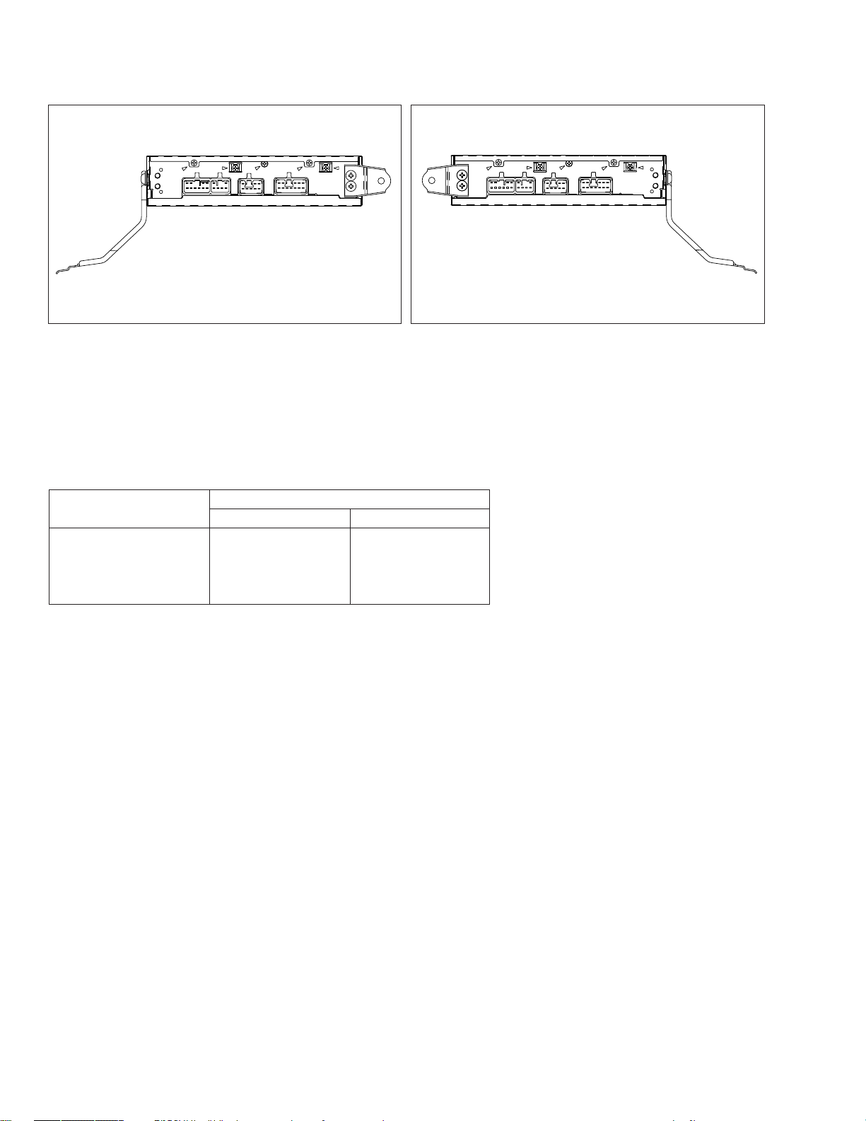
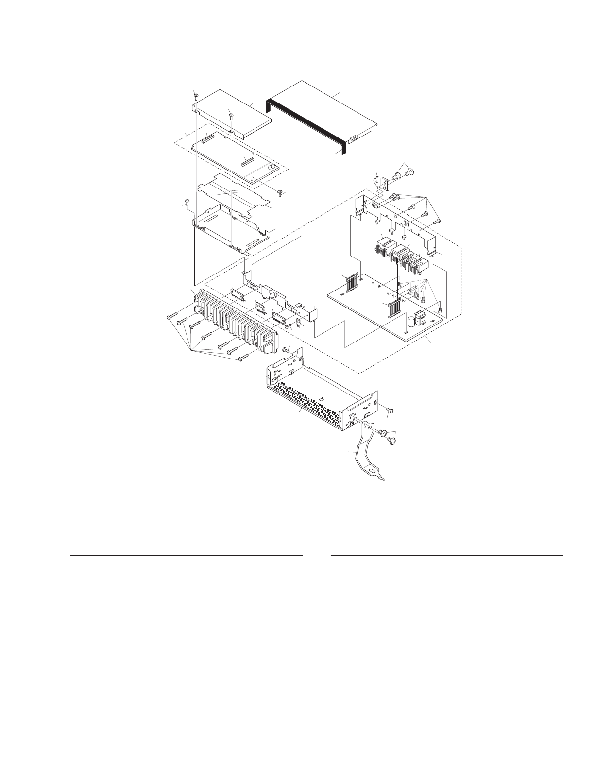
2. EXPLODED VIEWS AND PARTS LIST
2.1 EXTERIOR (GM-8506ZT/E)
NOTE:
- Parts marked by “*”are generally unavailable because they are not in our Master Spare Parts List.
- Screws adjacent to
∇ mark on the product are used for disassembly.
3
11
27
26
25
24
15
5
1
4
1
18
22
23
12
16
19
20
21
1
17
6
7
1
28
29
13
10
1
14
1
2
9
2
8
30
- EXTERIOR SECTION PARTS LIST
Mark No. Description Part No.
Mark No. Description Part No.
Page 4
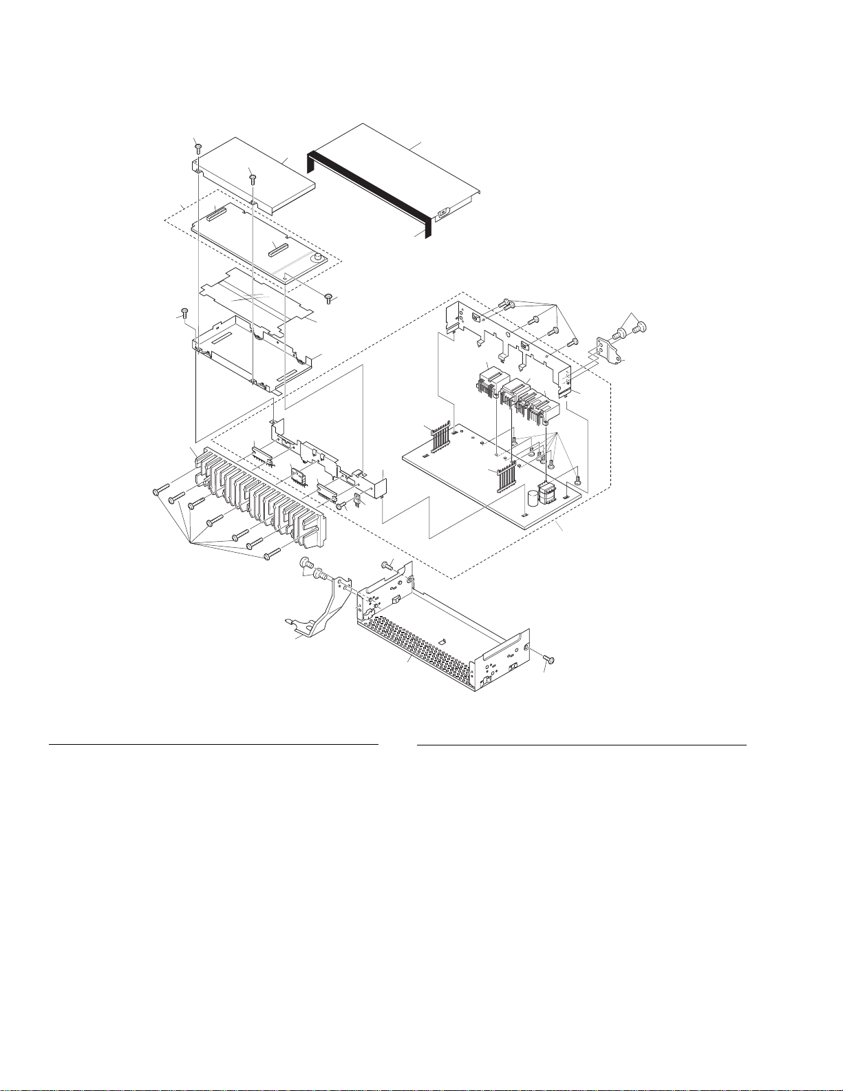
4
GM-8506ZT,8506ZT-91,8606ZT,8606ZT-91
1 Screw BMZ30P060FMC
2 Screw BMZ50P060FMC
3 Screw(M3x5) CBA1327
4 Chassis CNA1852
5 Case CNB2102
6 Shield CNC6809
7 Shield CNC6810
8 Bracket CNC6813
9 Bracket CNC6812
10 Insulator CNM5537
11 Heat Sink CNR1432
12 Amp Unit CWM6208
13 DSP Unit CWM7245
14 Screw IMS30P060FMC
15 Screw BMZ30P060FMC
16 Screw(M3x6) CBA1393
17 Bracket CNC6807
18 Holder CNC6808
19 Connector(CN901) CKM1222
20 Connector(CN902) CKM1244
21 Connector(CN903) CKM1245
22 Plug(CN905) CKS3631
23 Plug(CN906) CKS3631
24 IC(IC901) NJM7805FA
25 IC(IC801) TA8221AH1
26 IC(IC821) PAL001A
27 IC(IC851) TA8225H-LF1
28 Socket(CN51) CKS3632
29 Socket(CN52) CKS3632
* 30 Seal CNM5381
- EXTERIOR SECTION PARTS LIST
Mark No. Description Part No.
Mark No. Description Part No.
3
11
27
26
25
24
15
5
18
22
23
12
16
19
20
21
1
17
6
7
1
28
29
13
10
1
14
1
8
1
4
1
2
9
2
30
2.2 EXTERIOR (GM-8606ZT/E)
Page 5
5
GM-8506ZT,8506ZT-91,8606ZT,8606ZT-91
1
2
3
4
A
B
C
D
1
2
3
4
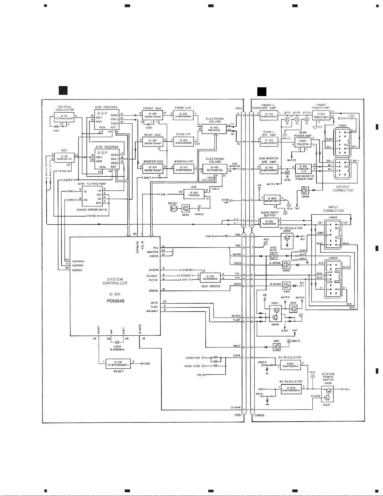
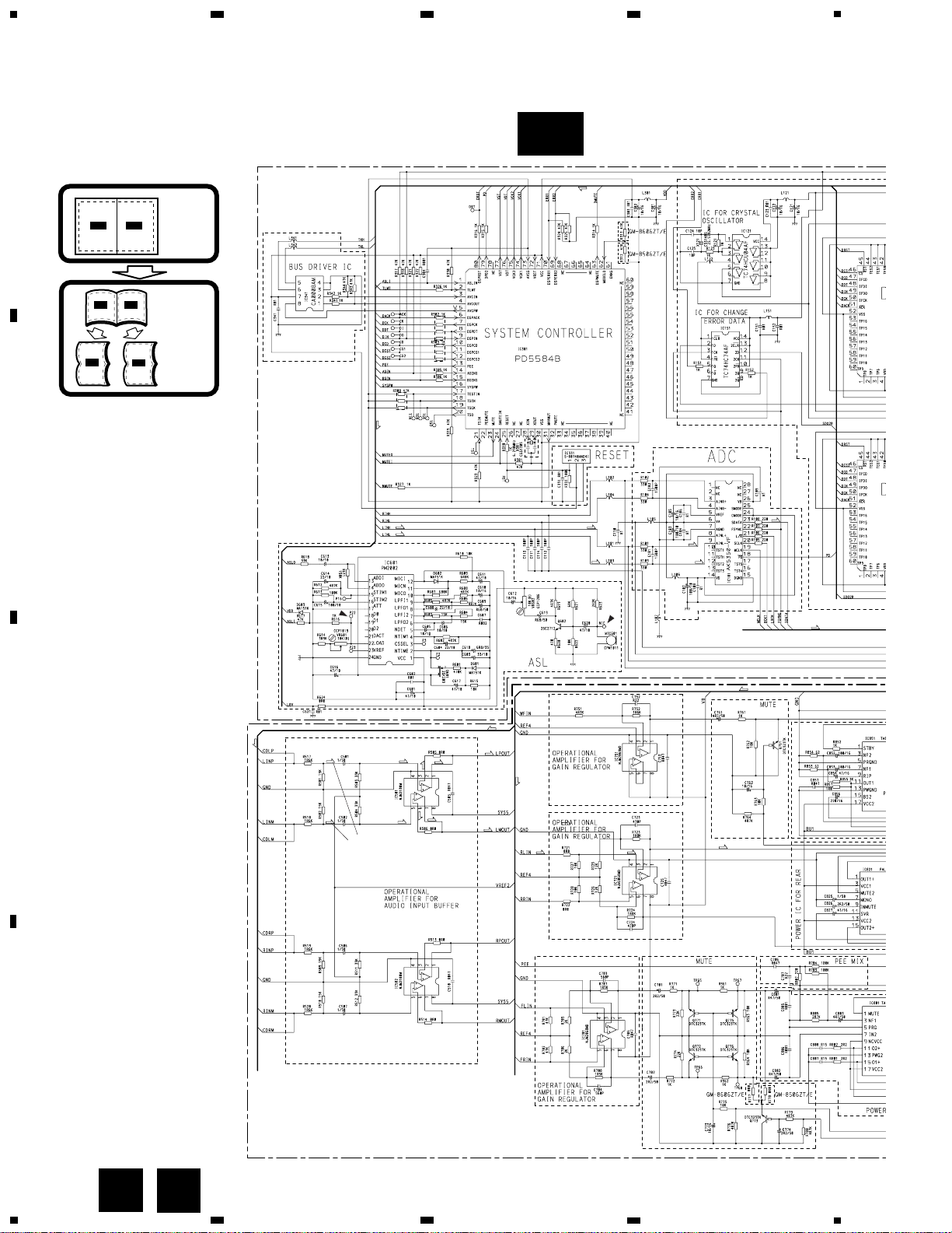
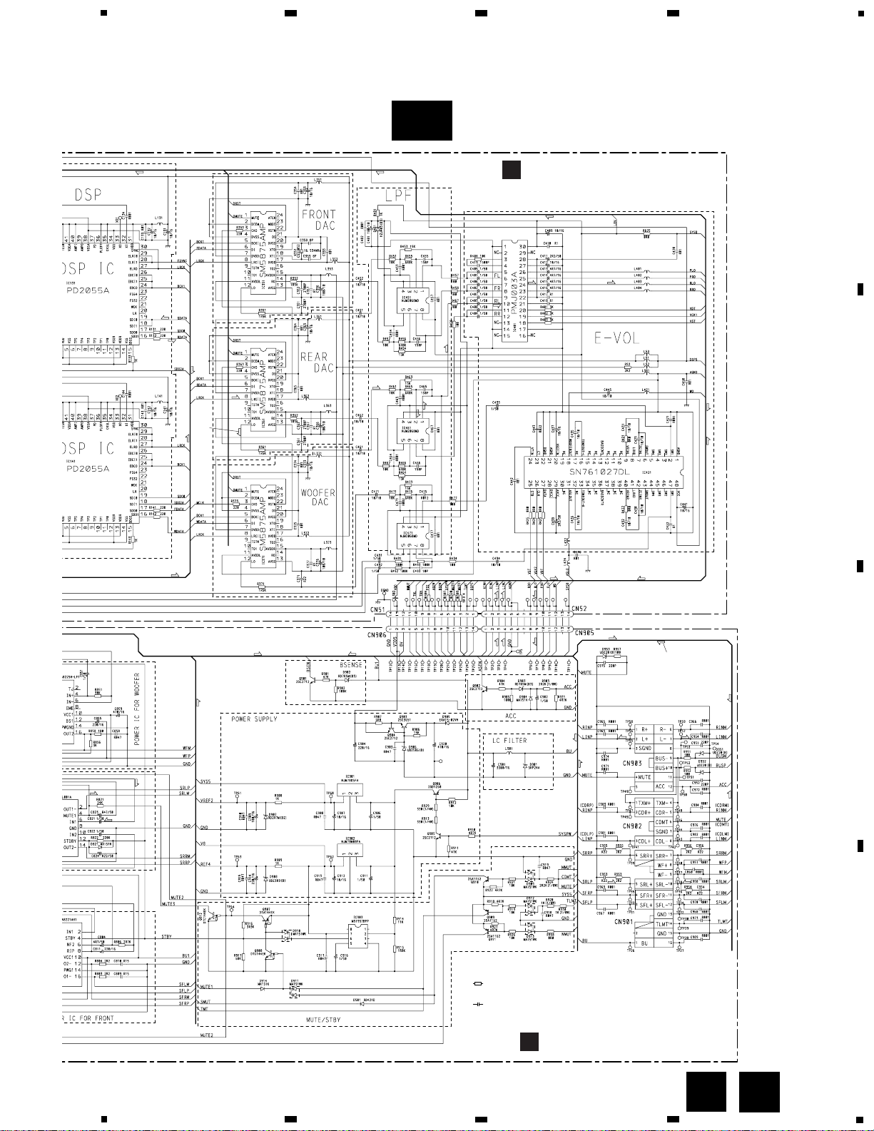
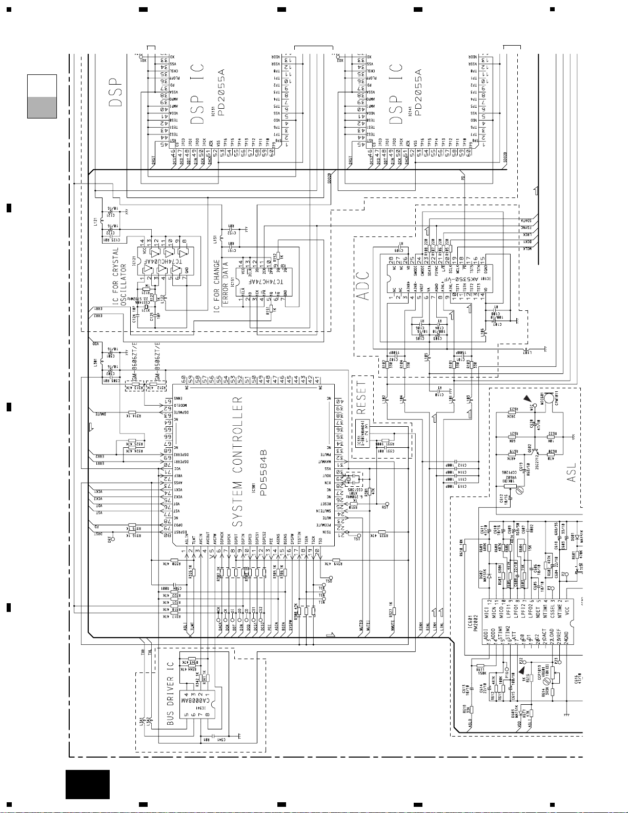
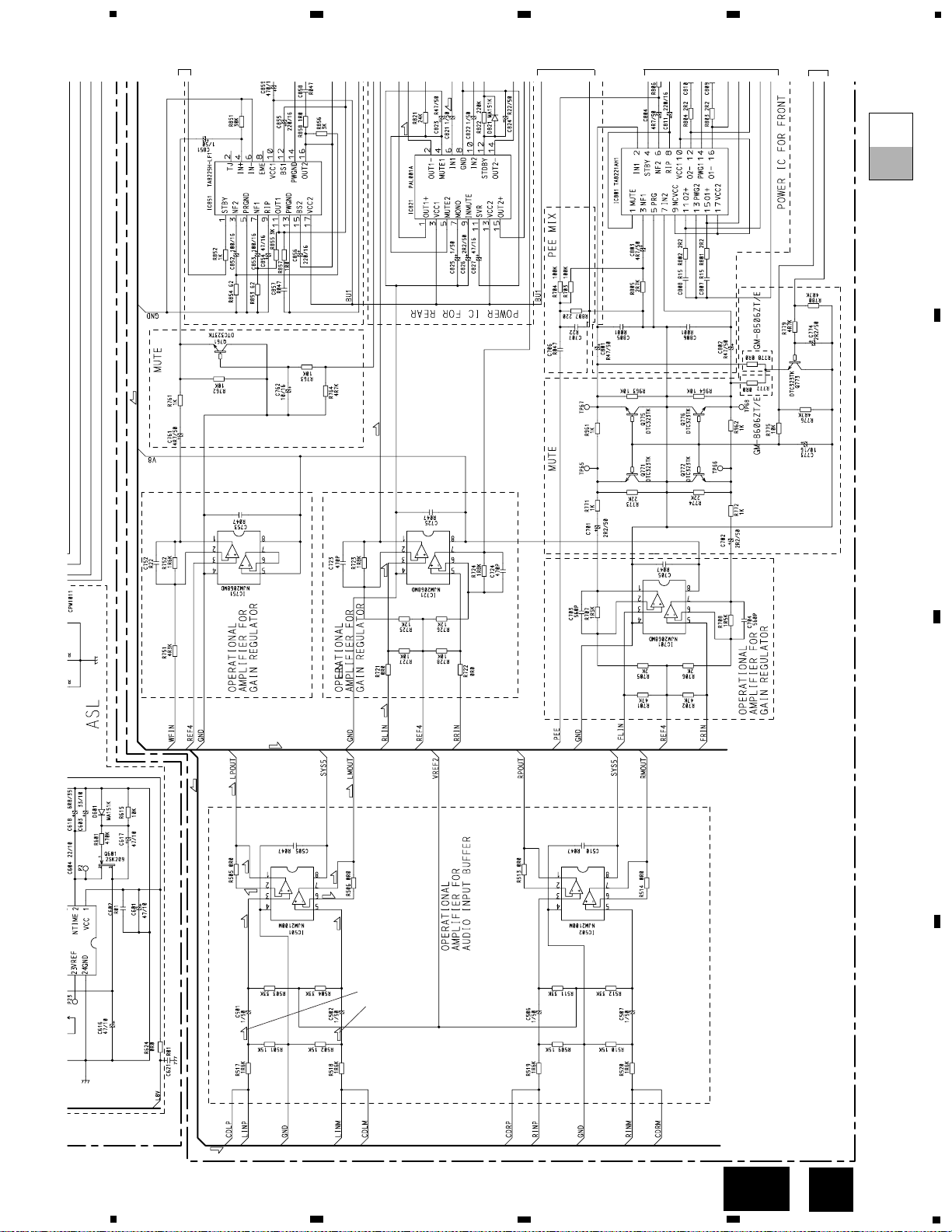
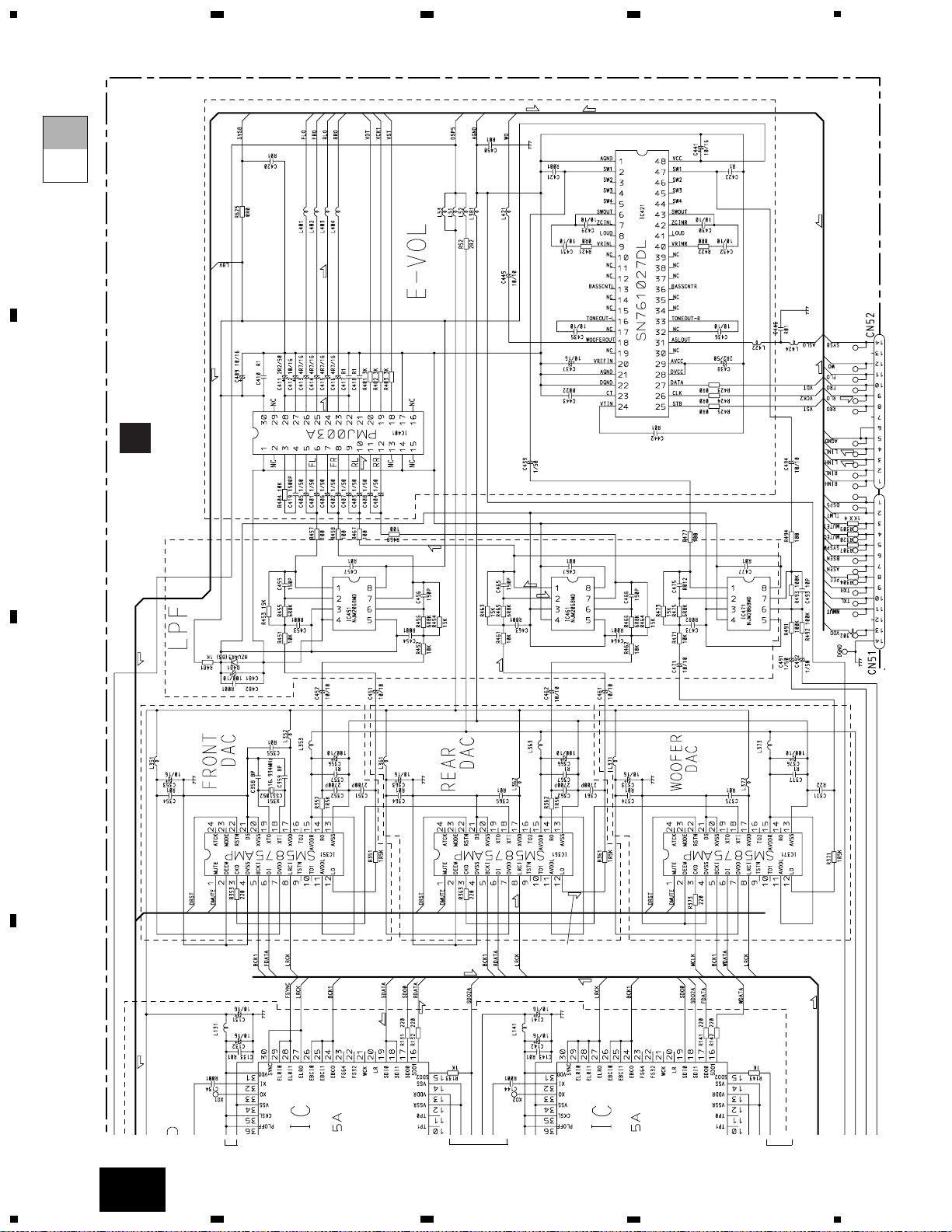
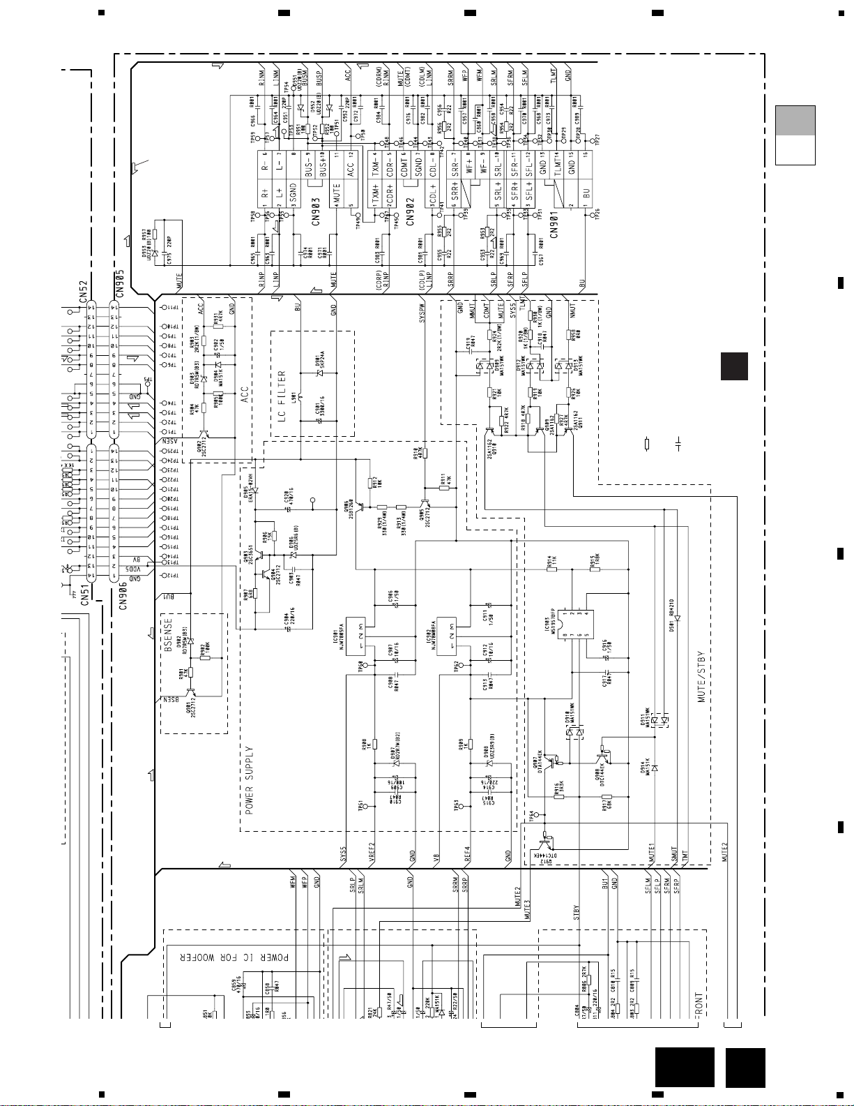
3. BLOCK DIAGRAM AND SCHEMATIC DIAGRAM
3.1 BLOCK DIAGRAM
A
B
DSP UNIT
AMP UNIT
Page 6
6
GM-8506ZT,8506ZT-91,8606ZT,8606ZT-91
A
1
234
B
C
D
12
34
3.2 SCHEMATIC DIAGRAM
Note: When ordering service parts, be sure to refer to “EXPLODED VIEWS AND PARTS LIST” or “ELECTRICAL
PARTS LIST”.
TAPE: -1.05dBs
CD: +6.95dBs
TUNER(EW): -9.05dBs
TUNER(UC):-14.05dBs
TAPE: -6.85dBs
4.9V
5.0V
4.9V
2.3V
4.9V
4.9V
4.9V
7.9V
7.5V
0.4V
1.0V
4.1V
3.4V
3.0V
3.0V
3.0V
3.0V
3.0V
3.4V
7.8V
7.9V
3.5V
3.5V
3.5V
3.5V
3.5V
3.5V
7.9V
5.0V
2.5V
5.0V
3.8V
3.8V
3.8V
7.9V
A-a A-b
A-a
A-b
A-b
A-a
Large size
SCH diagram
Guide page
Detailed page
A
A-a
B
Page 7
Decimal points for resistor
and capacitor fixed values
are expressed as :
2.2 2R2
0.022 R022
←
←
Symbol indicates a resistor.
No differentiation is made between chip resistors and
discrete resistors.
NOTE :
Symbol indicates a capacitor.
No differentiation is made between chip capacitors and
discrete capacitors.
A
DSP UNIT
B
AMP UNIT
TAPE: +0.2dBs
CD: +8.2dBs
TUNER(EW): -7.8dBs
TUNER(UC):-12.8dBs
TAPE: +25.15dBs
TAPE: -10.05dBs
CD: -3.55dBs
TAPE: -12.35dBs
CD: -5.85dBs
13.2V
3.8V
5.0V
3.8V
7.9V
7.6V
1.2V
1.8V
13.1V
13.2V
4.1V
13.2V
0.3mH
12.7V
13.2V
7.9V
3.8V
3.8V
3.8V
3.8V
3.8V
2.5V
2.5V
2.5V
2.5V
3.0V
2.5V
2.5V
4.9V
4.9V
7.9V
2.5V
4.9V
4.3V
4.3V
4.3V
4.3V
4.3V
4.3V
4.9V
2.5V
4.9V
2.5V
4.9V
2.5V
4.9V
4.3V
7.9V
4.3V
4.3V
4.3V
4.3V
7.9V
5.0V
4.9V
4.9V
7
GM-8506ZT,8506ZT-91,8606ZT,8606ZT-91
5
6
7
8
A
B
C
D
5
6
7
8
A-b
A
B
Page 8
8
GM-8506ZT,8506ZT-91,8606ZT,8606ZT-91
A
1
234
B
C
D
12
34
4.9V
5.0V
4.9V
2.3V
4.9V
4.9V
4.9V
7.9V
7.5V
0.4V
1.0V
4.1V
3.4V
3.0V
3.0V
3.0V
3.0V
3.0V
3.4V
7.8V
7.9V
3.5V
3.5V
3.5V
3.5V
3.5V
3.5V
A-a
A-b
A-a
1
2
3
Page 9
9
GM-8506ZT,8506ZT-91,8606ZT,8606ZT-91
5
6
7
8
A
B
C
D
5
6
7
8
A-a
A-b
TAPE: -1.05dBs
CD: +6.95dBs
TUNER(EW): -9.05dBs
TUNER(UC):-14.05dBs
TAPE: -6.85dBs
7.9V
3.5V
3.5V
3.5V
3.5V
7.9V
5.0V
2.5V
5.0V
3.8V
3.8V
3.8V
7.9V
A-a
B
4
5
6
7
Page 10
10
GM-8506ZT,8506ZT-91,8606ZT,8606ZT-91
A
1
234
B
C
D
12
34
A-a
A-b
A
DSP UNIT
TAPE: -10.05dBs
CD: -3.55dBs
TAPE: -12.35dBs
CD: -5.85dBs
7.9V
3.8V
3.8V
3.8V
3.8V
3.8V
2.5V
2.5V
2.5V
2.5V
3.0V
2.5V
2.5V
4.9V
4.9V
7.9V
2.5V
4.9V
4.3V
4.3V
4.3V
4.3V
4.3V
4.3V
4.9V
2.5V
4.9V
2.5V
4.9V
2.5V
4.9V
4.3V
7.9V
4.3V
4.3V
4.3V
4.3V
7.9V
5.0V
4.9V
4.9V
A-b
1
2
3
Page 11
Decimal points for resistor
and capacitor fixed values
are expressed as :
2.2 2R2
0.022 R022
←
←
Symbol indicates a resistor.
No differentiation is made between chip resistors and
discrete resistors.
NOTE :
Symbol indicates a capacitor.
No differentiation is made between chip capacitors and
discrete capacitors.
B
AMP UNIT
TAPE: +0.2dBs
CD: +8.2dBs
TUNER(EW): -7.8dBs
TUNER(UC):-12.8dBs
TAPE: +25.15dBs
13.2V
3.8V
5.0V
3.8V
7.9V
7.6V
1.2V
1.8V
13.1V
13.2V
4.1V
13.2V
0.3mH
12.7V
13.2V
7.9
3.8
3.8
3.8
3
3.8
2.5
2.5
3.0
4.9
7.9V
11
GM-8506ZT,8506ZT-91,8606ZT,8606ZT-91
5
6
7
8
A
B
C
D
5
6
7
8
A-a
A-b
A-b
B
4
5
6
7
Page 12
12
GM-8506ZT,8506ZT-91,8606ZT,8606ZT-91
A
1
234
B
C
D
12
34
4. PCB CONNECTION DIAGRAM
4.1 DSP UNIT
NOTE FOR PCB DIAGRAMS
1. The parts mounted on this PCB
include all necessary parts for
several destination.
For further information for
respective destinations, be sure
to check with the schematic diagram.
Capacitor
Connector
P.C.Board
Chip Part
SIDE A
SIDE B
2. Viewpoint of PCB diagrams
DSP UNIT
CN906
A
A
B
Page 13

13
GM-8506ZT,8506ZT-91,8606ZT,8606ZT-91
5
6
7
8
A
B
C
D
5
6
7
8
SIDE A
CN905
A
B
Page 14

14
GM-8506ZT,8506ZT-91,8606ZT,8606ZT-91
A
1
234
B
C
D
12
34
DSP UNIT
A
A
Page 15

15
GM-8506ZT,8506ZT-91,8606ZT,8606ZT-91
5
6
7
8
A
B
C
D
5
6
7
8
1
3
2
SIDE B
A
Page 16

16
GM-8506ZT,8506ZT-91,8606ZT,8606ZT-91
A
1
234
B
C
D
12
34
CN51
AMP UNIT
B
B
A
4.2 AMP UNIT
Page 17

17
GM-8506ZT,8506ZT-91,8606ZT,8606ZT-91
5
6
7
8
A
B
C
D
5
6
7
8
SIDE A
CN52
B
A
Page 18

18
GM-8506ZT,8506ZT-91,8606ZT,8606ZT-91
A
1
234
B
C
D
12
34
AMP UNIT
B
B
Page 19

19
GM-8506ZT,8506ZT-91,8606ZT,8606ZT-91
5
6
7
8
A
B
C
D
5
6
7
8
SIDE B
B
Page 20

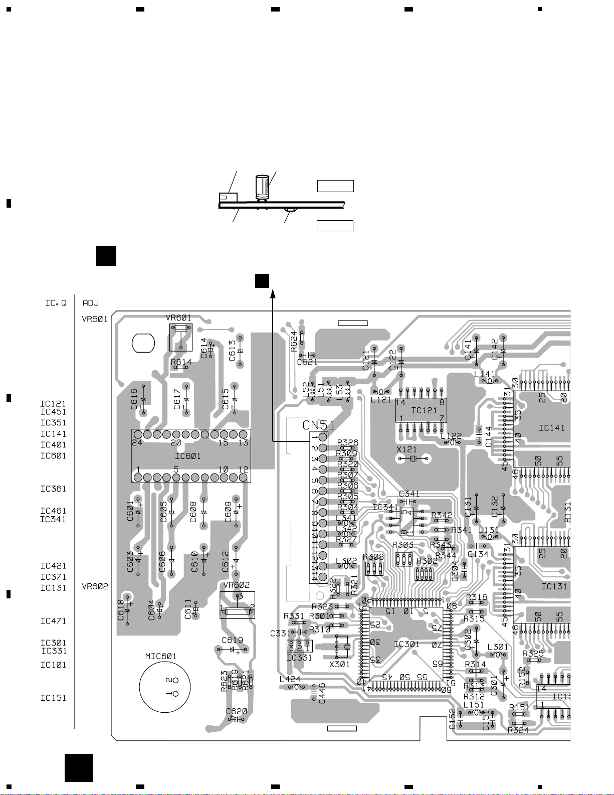
Unit Number : CWM7243(GM-8506ZT/E)
Unit Number : CWM7245(GM-8606ZT/E)
Unit Name : DSP Unit
MISCELLANEOUS
IC 101 IC AK5350-VF
IC 121 IC TC74HCU04AF
IC 131 IC PD2055A
IC 141 IC PD2055A
IC 151 IC TC74HC74AF
IC 301 IC PD5584B
IC 331 IC S-80740AND4I
IC 341 IC CA0008AM
IC 351 IC SM5875AMP
IC 361 IC SM5875AMP
IC 371 IC SM5875AMP
IC 401 IC PMJ003A
IC 421 IC SN761027DL
IC 451 IC NJM2068MD
IC 461 IC NJM2068MD
IC 471 IC NJM2068MD
IC 601 IC PM2002
Q 601 Transistor 2SK209
Q 602 Chip Transistor 2SC2712
D 481 Diode HZU4R3(B3)
D 601 Chip Diode MA151K
D 602 Chip Diode MA151K
D 603 Chip Diode MA151K
L 51 Chip-Inductor LCTA2R2J3225
L 52 Inductor LCTB1R0K3216
L 53 Chip-Inductor LCTA2R2J3225
L 101 Inductor LCTB1R0K2125
L 102 Inductor LCTB1R0K2125
L 103 Inductor LCTB1R0K2125
L 104 Inductor LCTB1R0K2125
L 105 Inductor LCTB4R7K2125
L 106 Inductor LCTB120K2125
L 107 Inductor LCTB1R0K2125
L 121 Inductor LCTBR82K2125
L 122 Inductor CTF1305
L 131 Inductor LCTBR82K2125
L 141 Inductor LCTBR82K2125
L 151 Inductor LCTB1R0K2125
L 301 Inductor LCTB1R0K2125
L 302 Inductor LCTB1R0K2125
L 341 Inductor CTF1305
L 342 Inductor CTF1305
L 351 Inductor LCTB1R0K2125
L 352 Inductor LCTB1R0K2125
L 353 Inductor LCTB120K2125
L 361 Inductor LCTB1R0K2125
L 362 Inductor LCTB1R0K2125
L 363 Inductor LCTB120K2125
L 371 Inductor LCTB1R0K2125
L 372 Inductor LCTB1R0K2125
L 373 Inductor LCTB120K2125
L 381 Inductor LCTB1R0K2125
L 401 Inductor LCTB1R0K2125
L 402 Inductor LCTB1R0K2125
L 403 Inductor LCTB1R0K2125
L 404 Inductor LCTB1R0K2125
L 421 Inductor LCTB1R0K2125
L 422 Inductor LCTB1R0K2125
L 424 Inductor LCTB1R0K2125
X 121 Radiator 22.5792MHz CSS1406
X 301 Ceramic Resonator 6.290MHz CSS1305
X 351 Crystal Resonator 16.9344MHz CSS1052
VR 601 Semi-fixed 10kΩ(B) CCP1019
VR 602 Semi-fixed 10kΩ(B) CCP1206
MIK 601 Microphone CPM1011
RESISTORS
R 52 RS1/10S2R2J
R 101 RS1/10S331J
R 102 RS1/10S331J
R 103 RS1/10S331J
R 104 RS1/10S331J
R 105 RS1/10S221J
R 106 RS1/10S221J
R 107 RS1/10S221J
R 108 RS1/10S221J
R 121 RS1/10S105J
R 123 RS1/10S102J
R 131 RS1/10S221J
R 132 RS1/10S221J
R 133 RS1/10S102J
R 141 RS1/10S221J
R 142 RS1/10S221J
R 143 RS1/10S102J
R 151 RS1/10S102J
R 152 RS1/10S102J
R 301 RS1/10S473J
R 302 1kΩ CCN1120
R 303 RA3C102J
R 304 RS1/10S102J
R 305 RS1/10S102J
R 306 RS1/10S102J
R 307 RS1/10S102J
R 308 RA3C473J
R 309 RS1/10S102J
R 310 RS1/10S102J
R 312 (GM-8506ZT/E) RS1/10S473J
20
GM-8506ZT,8506ZT-91,8606ZT,8606ZT-91
5. ELECTRICAL PARTS LIST
NOTE:
- Parts whose parts numbers are omitted are subject to being not supplied.
- The part numbers shown below indicate chip components.
Chip Resistor
RS1/_S___J,RS1/__S___J
Chip Capacitor (except for CQS.....)
CKS....., CCS....., CSZS.....
=====Circuit Symbol and No.===Part Name Part No.
--- ------ ------------------------------------------ -------------------------
=====Circuit Symbol and No.===Part Name Part No.
--- ------ ------------------------------------------ -------------------------
A
Page 21

21
GM-8506ZT,8506ZT-91,8606ZT,8606ZT-91
R 313 (GM-8606ZT/E) RS1/10S473J
R 314 RS1/10S102J
R 315 RS1/10S102J
R 316 RS1/10S102J
R 317 RS1/10S473J
R 318 RS1/10S473J
R 319 RS1/10S473J
R 320 RS1/10S102J
R 321 RS1/10S473J
R 322 RS1/10S473J
R 323 RS1/10S473J
R 324 RS1/10S473J
R 325 RS1/10S473J
R 326 RS1/10S102J
R 327 RS1/10S102J
R 330 RS1/10S473J
R 331 RS1/10S104J
R 341 RS1/10S102J
R 342 RS1/10S102J
R 343 RS1/10S473J
R 344 RS1/10S473J
R 351 RS1/10S152J
R 352 RS1/10S152J
R 353 RS1/10S221J
R 361 RS1/10S152J
R 362 RS1/10S152J
R 363 RS1/10S221J
R 371 RS1/10S152J
R 373 RS1/10S221J
R 401 RS1/10S302J
R 402 RS1/10S302J
R 403 RS1/10S302J
R 404 RS1/10S103J
R 421 RS1/10S0R0J
R 422 RS1/10S0R0J
R 423 RS1/10S0R0J
R 424 RS1/10S0R0J
R 425 RS1/10S0R0J
R 451 RS1/10S103J
R 452 RS1/10S103J
R 453 RS1/10S153J
R 454 RS1/10S153J
R 455 RS1/10S682J
R 456 RS1/10S682J
R 457 RS1/10S101J
R 458 RS1/10S101J
R 461 RS1/10S103J
R 462 RS1/10S103J
R 463 RS1/10S153J
R 464 RS1/10S153J
R 465 RS1/10S682J
R 466 RS1/10S682J
R 467 RS1/10S101J
R 468 RS1/10S101J
R 471 RS1/10S103J
R 473 RS1/10S153J
R 475 RS1/10S682J
R 477 RS1/10S101J
R 481 RS1/10S102J
R 491 RS1/10S104J
R 492 RS1/10S104J
R 493 RS1/10S104J
R 494 RS1/10S101J
R 601 RS1/10S474J
R 602 RS1/10S472J
R 603 RS1/10S153J
R 604 RS1/10S153J
R 605 RS1/10S472J
R 606 RS1/10S472J
R 607 RS1/10S684J
R 608 RS1/10S472J
R 609 RS1/10S682J
R 610 RS1/10S103J
R 611 RS1/10S154J
R 612 RS1/10S472J
R 613 RS1/10S104J
R 614 RS1/10S392J
R 615 RS1/10S103J
R 616 RS1/10S102J
R 617 RS1/10S473J
R 618 RS1/10S393J
R 619 RS1/10S472J
R 620 RS1/10S471J
R 621 RS1/10S683J
R 622 RS1/10S103J
R 623 RS1/10S222J
R 624 RS1/10S0R0J
R 625 RS1/10S0R0J
CAPACITORS
C 101 CKSQYB152K50
C 102 CKSQYB152K50
C 103 CEAL101M10
C 104 CKSQYB104K50
C 105 CEAL100M16
C 106 CKSQYB104K50
C 107 CEAL101M10
C 108 CKSQYB104K50
C 109 CKSQYB104K50
C 110 CKSQYB104K50
C 111 CCSQCH101J50
C 112 CCSQCH101J50
C 113 CCSQCH101J50
C 114 CCSQCH101J50
C 121 CEAL100M16
C 122 CEAL100M16
C 123 CKSQYB103K50
C 124 CCSQCH100J50
C 125 CCSQCH100J50
C 131 CEAL100M16
C 132 CEAL100M16
C 133 CKSQYB103K50
C 134 CKSQYB102K50
C 141 CEAL100M16
C 142 CEAL100M16
C 143 CKSQYB103K50
C 144 CKSQYB102K50
C 151 CKSQYB103K50
C 152 CKSQYB103K50
C 301 CEAL100M16
C 302 CEAL100M16
C 303 CKSQYB103K50
C 304 CKSQYB102K50
C 331 CKSQYB103K50
C 341 CKSQYB103K50
C 351 CKSQYB272K50
C 352 CKSQYB272K50
C 353 CEAL100M16
C 354 CKSQYB103K50
C 355 CKSQYB103K50
C 356 CEAL101M10
C 357 CKSQYB104K50
C 358 CCSQCH8R0D50
C 359 CCSQCH8R0D50
C 361 CKSQYB272K50
C 362 CKSQYB272K50
C 363 CEAL100M16
C 364 CKSQYB103K50
C 365 CKSQYB103K50
C 366 CEAL101M10
=====Circuit Symbol and No.===Part Name Part No.
--- ------ ------------------------------------------ -------------------------
=====Circuit Symbol and No.===Part Name Part No.
--- ------ ------------------------------------------ -------------------------
Page 22

C 367 CKSQYB104K50
C 371 CKSQYB224K16
C 373 CEAL100M16
C 374 CKSQYB103K50
C 375 CKSQYB103K50
C 376 CEAL101M10
C 377 CKSQYB104K50
C 401 CEALNP1R0M50
C 402 CEALNP1R0M50
C 403 CEALNP1R0M50
C 404 CEALNP1R0M50
C 405 CEALNP1R0M50
C 406 CEALNP1R0M50
C 407 CEALNP1R0M50
C 408 CEALNP1R0M50
C 409 CEAL100M16
C 410 CKSQYB104K50
C 411 CEAL2R2M50
C 412 CEAL100M16
C 413 CEALNP4R7M16
C 414 CEALNP4R7M16
C 415 CEALNP4R7M16
C 416 CEALNP4R7M16
C 417 CKSQYB104K50
C 418 CKSQYB104K50
C 419 CKSQYB152K50
C 420 CKSQYB103K50
C 421 CKSQYB102K50
C 422 CKSQYB104K50
C 429 CEALNP100M10
C 430 CEALNP100M10
C 431 CEALNP100M10
C 432 CEALNP100M10
C 435 CEALNP100M10
C 436 CEALNP100M10
C 437 CEAL100M16
C 438 CEAL2R2M50
C 439 CEALNP1R0M50
C 441 CEAL100M16
C 442 CKSQYB103K50
C 443 CKSQYB223K50
C 445 CEALNP100M10
C 446 CKSQYB103K50
C 450 CKSQYB103K50
C 451 CEALNP100M10
C 452 CEALNP100M10
C 453 CKSQYB102K50
C 454 CKSQYB102K50
C 455 CCSQCH151J50
C 456 CCSQCH151J50
C 457 CKSQYB103K50
C 461 CEALNP100M10
C 462 CEALNP100M10
C 463 CKSQYB102K50
C 464 CKSQYB102K50
C 465 CCSQCH151J50
C 466 CCSQCH151J50
C 467 CKSQYB103K50
C 471 CEALNP100M10
C 473 CKSQYB823K25
C 475 CKSQYB123K25
C 477 CKSQYB103K50
C 481 CEAL101M10
C 482 CKSQYB102K50
C 491 CEALNP1R0M50
C 492 CEALNP1R0M50
C 493 CCSQCH100J50
C 494 CEALNP100M10
C 601 CEJA470M10
C 602 CKSQYB103K50
C 603 CEJA330M10
C 604 CEAL220M10
C 605 CEALNP100M10
C 606 CEALNP100M10
C 607 CKSQYB823K25
C 608 CEALNP220M16
C 609 CEALR68M50
C 610 CEAL100M16
C 611 CEJA470M10
C 612 CEAL100M16
C 613 CEALNP100M10
C 614 CEAL220M10
C 615 CEJA101M10
C 616 CEJA470M10
C 617 CEJA470M10
C 618 CEAL6R8M35
C 619 CEALR68M50
C 620 CEJA470M10
C 621 CKSQYB103K50
Unit Number : CWM6207(GM-8506ZT/E)
Unit Number : CWM6208(GM-8606ZT/E)
Unit Name : Amp Unit
MISCELLANEOUS
IC 501 IC NJM2100M
IC 502 IC NJM2100M
IC 701 IC NJM2068MD
IC 721 IC NJM2068MD
IC 751 IC NJM2068MD
IC 801 IC TA8221AH1
IC 821 IC PAL001A
IC 851 IC TA8225H-LF1
IC 901 IC NJM7805FA
IC 902 IC NJM78M08FA
IC 903 IC M51957BFP
Q 761 Transistor DTC323TK
Q 771 Transistor DTC323TK
Q 772 Transistor DTC323TK
Q 773 Transistor DTC323TK
Q 775 Transistor DTC323TK
Q 776 Transistor DTC323TK
Q 901 Transistor 2SC2712
Q 902 Transistor 2SC2712
Q 903 Transistor 2SC3651
Q 904 Transistor 2SC2712
Q 905 Transistor 2SC2712
Q 906 Transistor 2SB1260
Q 907 Transistor DTA144EK
Q 908 Transistor DTC144EK
Q 909 Transistor 2SA1162
Q 910 Transistor 2SA1162
Q 911 Transistor 2SA1162
Q 912 Transistor DTC144EK
D 501 Diode RB421D
D 821 Chip Diode MA151K
D 901 Diode 5KP24A
D 902 Diode RD7R5M(B3)
D 903 Diode RD7R5M(B3)
D 904 Chip Diode MA151K
D 905 Diode ERA15-02VH
D 906 Diode UDZ5R6(B)
D 907 Diode RD2R7M(B2)
D 908 Diode UDZ3R9(B)
D 909 Chip Diode MA151WK
D 910 Chip Diode MA151WK
D 911 Chip Diode MA151WK
D 912 Chip Diode MA151WK
D 913 Chip Diode MA151WK
D 914 Chip Diode MA151K
22
GM-8506ZT,8506ZT-91,8606ZT,8606ZT-91
=====Circuit Symbol and No.===Part Name Part No.
--- ------ ------------------------------------------ -------------------------
=====Circuit Symbol and No.===Part Name Part No.
--- ------ ------------------------------------------ -------------------------
B
Page 23

D 951 Diode UDZ20(B)
D 952 Diode UDZ20(B)
D 953 Diode UDZ20(B)
L 901 Choke Coil 0.3mA CTH1079
RESISTORS
R 501 RS1/10S153J
R 502 RS1/10S153J
R 503 RS1/10S333J
R 504 RS1/10S333J
R 505 RS1/10S0R0J
R 506 RS1/10S0R0J
R 509 RS1/10S153J
R 510 RS1/10S153J
R 511 RS1/10S333J
R 512 RS1/10S333J
R 513 RS1/10S0R0J
R 514 RS1/10S0R0J
R 517 RS1/10S162J
R 518 RS1/10S162J
R 519 RS1/10S162J
R 520 RS1/10S162J
R 701 RS1/10S473J
R 702 RS1/10S473J
R 703 RS1/10S104J
R 704 RS1/10S104J
R 705 RS1/10S202J
R 706 RS1/10S202J
R 707 RS1/10S152J
R 708 RS1/10S152J
R 721 RS1/10S0R0J
R 722 RS1/10S0R0J
R 723 RS1/10S182J
R 724 RS1/10S182J
R 725 RS1/10S123J
R 726 RS1/10S123J
R 727 RS1/10S103J
R 728 RS1/10S103J
R 751 RS1/10S432J
R 752 RS1/10S162J
R 761 RS1/10S102J
R 762 RS1/10S103J
R 763 RS1/10S103J
R 764 RS1/10S472J
R 771 RS1/10S102J
R 772 RS1/10S102J
R 773 RS1/10S223J
R 774 RS1/10S223J
R 775 RS1/10S103J
R 776 RS1/10S472J
R 777 (GM-8606ZT/E) RS1/10S0R0J
R 778 (GM-8506ZT/E) RS1/10S0R0J
R 779 RS1/10S472J
R 780 RS1/10S472J
R 801 RS1/10S2R2J
R 802 RS1/10S2R2J
R 803 RS1/10S2R2J
R 804 RS1/10S2R2J
R 805 RS1/10S272J
R 806 RS1/10S272J
R 807 RS1/10S221J
R 821 RS1/10S243J
R 822 RS1/10S224J
R 851 RS1/10S303J
R 852 RS1/10S102J
R 853 RS1/10S620J
R 854 RS1/10S620J
R 855 RS1/10S302J
R 856 RS1/10S302J
R 857 RS1/10S1R0J
R 858 RS1/10S1R0J
R 901 RS1/10S473J
R 902 RS1/10S104J
R 903 RS1/8S222J
R 904 RS1/10S473J
R 905 RS1/10S104J
R 906 RS1/10S153J
R 907 RS1/10S6R8J
R 908 RS1/10S102J
R 909 RS1/10S102J
R 910 RS1/10S472J
R 911 RS1/10S473J
R 912 RS1/10S103J
R 913 RS1/4S331J
R 914 RS1/10S113J
R 915 RS1/10S182J
R 916 RS1/10S332J
R 917 RS1/10S683J
R 918 RS1/10S472J
R 919 RS1/10S103J
R 920 RS1/8S102J
R 921 RS1/10S103J
R 922 RS1/10S472J
R 924 RS1/8S222J
R 926 RS1/10S103J
R 927 RS1/10S472J
R 929 RS1/4S331J
R 930 RS1/8S102J
R 931 RS1/10S472J
R 951 RS1/10S101J
R 952 RS1/10S101J
R 953 RS1/10S2R2J
R 954 RS1/10S2R2J
R 955 RS1/10S2R2J
R 956 RS1/10S2R2J
R 957 RS1/10S101J
R 958 RS1/10S0R0J
R 961 RS1/10S102J
R 962 RS1/10S102J
R 963 RS1/10S103J
R 964 RS1/10S103J
CAPACITORS
C 501 CEJANP1R0M50
C 502 CEJANP1R0M50
C 505 CKSQYB473K50
C 506 CEJANP1R0M50
C 507 CEJANP1R0M50
C 510 CKSQYB473K50
C 701 CEANL2R2M50
C 702 CEANL2R2M50
C 703 CCSQCH561J50
C 704 CCSQCH561J50
C 705 CKSQYB473K50
C 706 CKSQYB473K50
C 707 CKSQYB224K16
C 723 CCSQCH471J50
C 724 CCSQCH471J50
C 725 CKSQYB473K50
C 752 CKSQYB224K16
C 753 CKSQYB473K50
C 761 CEANL4R7M50
C 762 CEJA100M16
23
GM-8506ZT,8506ZT-91,8606ZT,8606ZT-91
=====Circuit Symbol and No.===Part Name Part No.
--- ------ ------------------------------------------ -------------------------
=====Circuit Symbol and No.===Part Name Part No.
--- ------ ------------------------------------------ -------------------------
Page 24

C 773 CEJA100M16
C 774 CEJA2R2M50
C 801 CEANLR47M50
C 802 CEANLR47M50
C 803 CEANL4R7M50
C 804 CEANL4R7M50
C 805 CKSQYB102K50
C 806 CKSQYB102K50
C 807 CFTNA154J50
C 808 CFTNA154J50
C 809 CFTNA154J50
C 810 CFTNA154J50
C 811 CEAS221M16
C 821 1µF/50V CCH1296
C 822 1µF/50V CCH1296
C 823 CEJAR47M50
C 824 CEJAR22M50
C 825 CEJA1R0M50
C 826 CEJA2R2M50
C 827 CEJA470M16
C 851 CEANL1R0M50
C 852 CEANL101M16
C 853 CEANL101M16
C 854 CEJA470M16
C 855 CEAS221M16
C 856 CEAS221M16
C 857 CFTNA473J50
C 858 CFTNA473J50
C 859 CEAS471M16
C 860 CQMA102J50
C 901 3300µF/16V CCH1163
C 902 CEJA1R0M50
C 903 CKSQYB473K50
C 904 CEAS221M16
C 906 CEHAR010M50
C 907 CEHAR100M16
C 908 CKSQYB473K50
C 909 CEAS101M16
C 910 CKSQYB473K50
C 911 CEJA1R0M50
C 912 CEJA100M16
C 913 CKSQYB473K50
C 914 CEAS221M16
C 915 CKSQYB473K50
C 916 CEJA1R0M50
C 917 CKSQYB473K50
C 918 CKSQYB473K50
C 919 CKSQYB473K50
C 920 CEAS471M16
C 951 CKSQYB221K50
C 952 CKSQYB221K50
C 953 CKSQYB224K16
C 954 CKSQYB224K16
C 955 CKSQYB224K16
C 956 CKSQYB224K16
C 957 CKSQYB102K50
C 958 CKSQYB102K50
C 963 CKSQYB102K50
C 964 CKSQYB102K50
C 965 CKSQYB102K50
C 966 CKSQYB102K50
C 967 CKSQYB102K50
C 968 CKSQYB102K50
C 969 CKSQYB102K50
C 970 CKSQYB102K50
C 971 CKSYB102K50
C 972 CKSYB102K50
C 973 CKSYB102K50
C 974 CKSYB102K50
C 975 CKSQYB221K50
C 976 CKSQYB102K50
C 981 CKSQYB102K50
C 982 CKSQYB102K50
C 983 CKSQYB102K50
C 984 CKSQYB102K50
C 989 CKSQYB102K50
24
GM-8506ZT,8506ZT-91,8606ZT,8606ZT-91
=====Circuit Symbol and No.===Part Name Part No.
--- ------ ------------------------------------------ -------------------------
=====Circuit Symbol and No.===Part Name Part No.
--- ------ ------------------------------------------ -------------------------
Page 25

25
GM-8506ZT,8506ZT-91,8606ZT,8606ZT-91
6. ADJUSTMENT
- Connection Diagram
H/U
KEX-M8506ZT/UC
KEX-M9506ZT/UC
KEX-M8606ZT/EW
KEX-M8706ZT/EW
DSP AMP
GM-8506ZT/E
GM-8606ZT/E
20P 12P
12P
10P 8P6P
20P 12P
10P 8P6P
10P
10P
CD Changer
CDX-M8076ZT/E
GGD1167
GGD1144
12P
14P 8P
Display
10P
10P
12P
GGD1148
14P 8P
GGD1236
Page 26

26
GM-8506ZT,8506ZT-91,8606ZT,8606ZT-91
H/U
KEX-M8406ZT/UC
KEX-M9406ZT/UC
KEX-M9006ZT/EW
KEX-M9106ZT/EW
DSP AMP
GM-8506ZT/E
GM-8606ZT/E
20P 12P
12P10P 8P6P
20P 12P
10P 8P6P
10P
10P
CD Changer
CDX-M8076ZT/E
CDX-M8106ZT/E
GGD1167
GGD1144
20P
12P
12P
12P
GGD1148
12P
14P 8P
GGD1236
Page 27

27
GM-8506ZT,8506ZT-91,8606ZT,8606ZT-91
- Jig
GGD1153
Page 28

28
GM-8506ZT,8506ZT-91,8606ZT,8606ZT-91
ASL SECTION
Preset conditions
1. Set VR601 and VR602 around the center of the adjustable range.
2. Ground pins 3 and 16 of IC601.
Step Input Output Adjustment
No. (MIC) (Pin 22) Adj.point Spec. Conditions
1 By using an oscillator, apply a sine Observe the output at VR602 1.2±0.3V Pin 16:Ground
wave of 7Hz/2.5mV to the MIC Pin 22 on a DC voltmeter Pin 3:Open
terminal (+) via a 600-ohm resistor. (pointer-type). Wait for 20 seconds.
2 By using an oscillator, apply a sine Observe the output at VR601 4.6±0.1V Pin 16:Ground
wave of 7Hz/79mV to the MIC Pin 22 on a digital Pin 3:Ground
terminal (+) via a 600-ohm resistor. multimeter.
3 Repeat Steps 1 and 2 until doth adjustments satisfy the specifications.
4 By using the jig(CAN-906,CAN-912), Observe the output at VR602 3.3±0.1V Pin 16:Ground
apply a sine wave of 100dB-SPL Pin 22 on a digital Pin 3:Open
voltage directly to the MIC terminal. multimeter.
5 End
To connect the Amp unit and the DSP unit, use Jig GGD1153.
VR602
VR601
DSP UNIT
MIC
DSP UNIT
Oscillator
600Ω
DC meter
Digital multi
meter
CN903 CN902 CN901
WF+
L-
TMUT
R+
R-
BUS-
BUS+
SFL-
GND
SFL+
ACC
WF-
L+
SRL+
SRR-
SGND
SRR+
SRL-
MUTE
CN901
CN903
BU
DC Regulated
Power Supply
13.2V
13.2V
TOP VIEW
BOTTOM VIEW
AMP UNIT
22pin
SFR-
SFR+
IC601
GND
0V
0V
Page 29

29
GM-8506ZT,8506ZT-91,8606ZT,8606ZT-91
7. GENERAL INFORMATION
7.1 DIAGNOSIS
7.1.1 DISASSEMBLY
- Removing the DSP Unit(Fig.2)
1.Remove the three screws C, and remove the upper
Shield.
2.Remove the screw D.
3.Disconnect connectors CN51 and CN52 from CN905
and CN906 respectively by pulling them upwards.
4.Release the DSP Unit from four stoppers marked with
arrows and remove the DSP Unit.
Fig.2
Fig. 1
A
B
B
B
D
CN51
CN52
C
C
CN905
CN906
C
Case
Heat Sink
Shield
Shield
DSP Unit
- Removing the Case(Fig.1)
1.Remove the Seal marked with arrows.
2.Remove the seven screws A, seven screws B, and
then remove the Case and Heat Sink.
Page 30

30
GM-8506ZT,8506ZT-91,8606ZT,8606ZT-91
7.1.2 CONNECTOR FUNCTION DESCRIPTION
TLMT
GND
SFL+
SFL-
WF+
WF-
SRL-
SRR+
SRL+
SRR-
SGND
TXM-
TXM+
L+
R+
L-
R-
BUS-
BUS+
ACC
MUTE
N-MU
CDR+
CDR-
CDMT
SGND
CDL+
CDL-
BU
SFR+
SFR-
GND
A
B
C
A
B
C
Page 31

31
GM-8506ZT,8506ZT-91,8606ZT,8606ZT-91
7.2 IC
PD2055A
Page 32

32
GM-8506ZT,8506ZT-91,8606ZT,8606ZT-91
- Pin Functions (PD5584B)
Pin No. Pin Name I/O Format Function and Operation
1 ASLIN I Difference of noise and signal input
2 TLMT I TEL mute input
3 AVCIN I AVC-LAN data input
4 AVCOUT O C AVC-LAN data output
5 AVCPW O C AVC-LAN driver power supply output
6 DSPACK I DSP-IC ACK input
7 DSPCK O C DSP serial clock output
8 DSPDT O C DSP data output
9 DSPIN I DSP serial data input
10 DSPCD O DSP command/data output
11 DSPCS1 O C TC9332F chip select 1
12 DSPCS2 O C TC9332F chip select 2
13 PEE O C Beep tone output
14 ASENS I ACC power sense input
15 BSEN I Back up power sense input
16 SYSPW O C System power supply control output
17 TESTIN I Test program start input
18 TSEN I Test enable input
19 TSCK O C Test program clock output
20 TSO O C Test program serial output
21 TSIN I Test data input
22 NC Not used
23 MUTE O C Mute output
24 SMUTEIN I System mute input
25 RESET I Reset input
26,27 NC Not used
28 XIN I Crystal oscillating element connection pin
29 XOUT O Crystal oscillating element connection pin
30 VSS GND
31 NAVMUT O C Navigation mute output
32–61 NC Not used
62 MODEL0 I Model select input
63 DSPMUTE O C DSP mute output
64–68 NC Not used
69 DSPERR2 I DSP error detect input 2
70 DSPERR1 I DSP error detect input 1
71 VCC 5V
72 VREF I A/D converter reference voltage input
73 AVSS I A/D GND
74 VCK1 O C Clock output for electronic volume
75 VCK2 O C Clock output electronic volume 2
76 VDT O C Data output for electronic volume
77 VST O C Strobe pulse output for electronic volume
78 NC Not used
79 DPD2 O C A/D converter offset calibration output
80 DSPRST O C DSP reset control
IC's marked by* are MOS type.
Be careful in handling them because they are very
liable to be damaged by electrostatic induction.
Format Meaning
C C MOS
*PD5584B
20
21
1
80
40
41
61
60
Page 33

33
GM-8506ZT,8506ZT-91,8606ZT,8606ZT-91
7.3 EXPLANATION
7.3.1 OPERATIONAL FLOW CHART
Reset Start---OFF ---Power ON
<<JUDGMENT>>
Test program check(Unit checker)
- TESTIN HI/LOW input
Unit checker program
TESTIN HI input
TESTIN LOW input
<<JUDGMENT>>
Back up, ACC confirmation
- ASENS/BSENS
Micon oscillation stop
(Electronic power save)
ASENS LOW input and BSENS LOW input
• ACC/Back up ON
Main loop
<<JUDGMENT>>
Bus communication Normal/Error
<<JUDGMENT>>
System ON/OFF
- OFF status
=System ON waiting
• Power OFF(SYSPW)
• Mute ON(MUTE)
- ON status
=System OFF waiting
• Power ON(SYSPW)
• Mute ON(MUTE)
• BEEP output available
<<JUDGMENT>>
DSP error confirmation
• communication error,Serial IF
• processing error
(DSPERR1/2)
• Volume refresh
<<JUDGMENT>>
ACC/Back up ON/OFF
START
| Hard ware reset cancel
Main loop
Error return
• DSP reset(DSPRST)
| About 1 second
Error(Communication error)
| Forcibly OFF
ASENS HI input
or
BSENS HI input
Normal(Main unit communication normal)
OFF
ON
Normal operation
DSP error
ACC ON/Back up ON
ASENS HI input
or
BSENS HI input
ASENS LOW input
and
BSENS LOW input
Page 34

34
GM-8506ZT,8506ZT-91,8606ZT,8606ZT-91
- DSP error check (Normal)
DSPERR1
DSPERR2
DSPCS1
DSPCS2
DSPCK
4mS interval
(Periodical communication)
DSPCS1
DSPCS2
DSPCK
- Electronic volume refresh (Normal)
Electronic VR IF
VDT
VCK1
VCK2
VST
About 500mS interval
- DSP error check ---Error continuation
DSPRST
About 1S interval
Both terminals confirmation
every 4mS
Page 35

35
GM-8506ZT,8506ZT-91,8606ZT,8606ZT-91
7.3.2 SYSTEM BLOCK DIAGRAM
H/U
PWR
AMP
CD
EMV
(OTHER MAKERS)
NAVIGATION
ECU
(OTHER MAKERS)
VISION
+B, ACC
+B, ACC
+B, ACC
KEX-M8506ZT/UC
KEX-M8606ZT/EW
KEX-M8706ZT/EW
GM-8506ZT/E
GM-8606ZT/E
CDX-M8076ZT/E
CDX-M8176ZT/E
H/U
PWR
AMP
CD
+B, ACC
+B, ACC
+B, ACC
KEX-M8406ZT/UC
KEX-M9006ZT/EW
KEX-M9106ZT/EW
GM-8506ZT/E
GM-8606ZT/E
CDX-M8076ZT/E
CDX-M8176ZT/E
VEHICLE
POWER SUPPLY(+B, ACC)
BUS
SIGNAL(SOUND, VISION)
- NAVIGATION SYSTEM(7SP)
- (7SP)
Page 36

36
GM-8506ZT,8506ZT-91,8606ZT,8606ZT-91
7.3.3 Service Mode For DSP Amplifier
1. Outline
This specifications details operation according to our
suggestion for answering complaint about sound
quality in audio systems. It is based on an assumption that a dealer or service person operate the product to solve the problem.
2. Sound Quality Service Mode Function
Sound Quality Service mode has the following functions:
1 Frequency characteristics adjustment : Specifies
two points (frequency/dB value) of equalizer (EQ)
to adjust frequency characteristics. Also adjusts
attenuation.
2 Level adjustment : Adjusts sound levels of the
front and rear speakers and woofer.
3. Activating Sound Quality Service Mode
Use the following steps to activate Sound Quality
Service mode.
1 Confirm that ACC is ON, then activate Dialogue
mode.
(Operate according to the method of activation of
diagnosis mode specified for the system.)
2 Press the [AM] button of H/U in the MENU screen
in Diagnosis mode .
The system enters Sound Quality mode. Then, the
system beeps one time and displays “AUDIO.” You
cannot return to Dialogue mode by pressing a button
from Sound Quality Service mode.
4. Canceling Sound Quality Service mode
Setting ACC to OFF cancels Sound Quality Service
mode. After that, the system will maintain sound
quality set in Sound Quality Service mode.
Normal
Diagnosis mode
(Menu Screen)
Sound Quality
Service mode
Entering Dialogue mode
Canceling Dialogue mode
Press [AM]
for five seconds.
Acc off Additional processing
Flowchart of activation/cancellation of Sound Quality Service mode
Page 37

37
GM-8506ZT,8506ZT-91,8606ZT,8606ZT-91
Flowchart of displays in Sound Quality Adjustment mode
Displaying "AUDIO"
Displaying "P1 XXX"
FM1/2
Displaying "P2 XXX"
FM1/2
Displaying "L XX"
FM1/2
FM1/2
Displaying "F XX"
Displaying "R XX"
Displaying "W XX"
TAPE
TAPE
TAPE
TAPE
Frequency characteristics
adjustment function
Level adjustment function
Sound Quality Service mode
Page 38

38
GM-8506ZT,8506ZT-91,8606ZT,8606ZT-91
5. Details
1 Frequency characteristics adjustment function
• The system changes submodes cyclically every
time the [FM1/2] button is pressed when
"AUDIO" is displayed.
Set EQ Point 1 t Set EQ Point 2 t Set attenuation t "AUDIO"
• Set EQ Point 1
The system displays “P1” and EQ management
number. The EQ management number
ascends/descends every time the UP/DOWN button is pressed.The EQ management number consists of three digits (000 to 286). Initial value is
000 (no setting).
• Set EQ Point 2
The system displays “P2” and EQ management
number. The EQ management number
ascends/descends every time the UP/DOWN button is pressed. The EQ management number
consists of three digits (000 to 176). Initial value
is 000 (no setting).
• Set attenuation
The system displays “L” and attenuation value.
Use the UP/DOWN button to change attenuation
within a range from 0 to -20 dB at increments of
1 dB. Attenuation value is shown in two digits
from 00 to 20 (20 = -20 dB). Initial value is 00 (no
setting).
2 level adjustment function
• The system changes submodes cyclically every
time the [TAPE] button is pressed when "AUDIO"
is displayed.
Set front t Set rear t Set woofer t “AUDIO”
• Set front
The system displays "F" and level value.Use the
UP/DOWN button to change level value within a
range from 0 to -80 dB at increments of 1 dB.
Level value is shown in two digits from 00 to 80
(80 = -80 dB). Initial value is 00 (no setting).
• Set rear
The system displays "R" and level value. Use the
UP/DOWN button to change level value within a
range from 0 to -80 dB at increments of 1 dB.
Level value is shown in two digits from 00 to 80
(80 = -80 dB). Initial value is 00 (no setting).
• Set woofer
The system displays "W" and level value. Use the
UP/DOWN button to change level value within a
range from 0 to -80 dB at increments of 1 dB.
Level value is shown in two digits from 00 to 80
(80 = -80 dB). Initial value is 00 (no setting).
Notes:
1) Pressing the TAPE button during adjustment of frequency characteristics is invalid. Pressing the
[FM1/2] button during level adjustment is invalid.
2) The UP/DOWN button mentioned above means the
[SEEK] key.
Page 39

39
GM-8506ZT,8506ZT-91,8606ZT,8606ZT-91
8. SPECIFICATIONS
Power source . . . . . . . . . . . . .13.2±0.1V(10.5-16.0V)
Grounding . . . . . . . . . . . . . . . .NEGATIVE TYPE
Electrode dark current . . . . . .1mA or less(13.2V)
Dimensions (No bracket) . . . .215mm(W)x50mm(H)x130mm(D)
Weight . . . . . . . . . . . . . . . . . . .1.325kg
Maximum output power . . . .50W or more(Front)
36W or more(Rear)
55W or more(Woofer)
Page 40

GM-8506ZT,8506ZT-91,8606ZT,8606ZT-91
PIONEER CORPORATION 4-1, Meguro 1-Chome, Meguro-ku, Tokyo 153-8654, Japan
PIONEER ELECTRONICS SERVICE INC. P.O.Box 1760, Long Beach, CA 90801-1760 U.S.A.
PIONEER EUROPE NV Haven 1087 Keetberglaan 1, 9120 Melsele, Belgium
PIONEER ELECTRONICS ASIACENTRE PTE.LTD. 253 Alexandra Road, #04-01, Singapore 159936
C PIONEER CORPORATION 2000
K-ZZB. JULY 2000 Printed in Japan
 Loading...