

查询TEA1211供应商
INTEGRATED CIRCUITS
DATA SH EET
TEA1211HN
High efficiency auto-up/down
DC/DC converter
Preliminary specification
Supersedes data of 2003 Aug 06
2003 Oct 13

Philips Semiconductors Preliminary specification
High efficiency auto-up/down
DC/DC converter
CONTENTS
1 FEATURES
2 APPLICATIONS
3 GENERAL DESCRIPTION
4 ORDERING INFORMATION
5 BLOCK DIAGRAM
6 PINNING
7 FUNCTIONAL DESCRIPTION
7.1 Introduction
7.2 Control mechanism
7.2.1 PWM
7.2.2 PFM
7.2.3 Switching sequence
7.3 Adjustable output voltage
7.4 Start-up
7.5 Under voltage lockout
7.6 Shut-down
7.7 Power switches
7.8 Synchronous rectification
7.9 PWM-only mode
7.10 External synchronisation
7.11 Current limiter
7.12 I2C-bus serial interface
7.12.1 Characteristics of the I2C-bus
7.12.2 START and STOP conditions
7.12.3 Bit transfer
7.12.4 Acknowledge
7.13 I2C-bus protocol
7.13.1 Addressing
7.13.2 Data
7.13.3 Write Cycle
TEA1211HN
8 LIMITING VALUES
9 THERMAL CHARACTERISTICS
10 CHARACTERISTICS
11 APPLICATION INFORMATION
11.1 Typical Li-Ion, 2- or 3-cell application with
I2C-bus programming
11.2 Component selection
11.2.1 Inductor
11.2.2 Capacitors
11.2.3 Schottky diodes
11.2.4 Feedback resistors
11.2.5 Current Limiter
12 PACKAGE OUTLINE
13 SOLDERING
13.1 Introduction to soldering surface mount
packages
13.2 Reflow soldering
13.3 Wave soldering
13.4 Manual soldering
13.5 Suitability of surface mount IC packages for
wave and reflow soldering methods
14 DATA SHEET STATUS
15 DEFINITIONS
16 DISCLAIMERS
17 PURCHASE OF PHILIPS I2C COMPONENTS
2003 Oct 13 2
Philips Semiconductors Preliminary specification
High efficiency auto-up/down
DC/DC converter
1 FEATURES
• I2C-bus programmable output voltage range of
1.5 V to 5.5 V
• Single inductor topology
• High efficiency up to 94 % over wide load range
• Wide input range; functional from 2.55 V up to 5.5 V
• 1.7 A maximum input and output current
• Low quiescent power consumption
• 600 kHz switching frequency
• Four integrated very low R
• Synchronizable to external clock
• Externally adjustable current limit for protection and
efficient battery use in case of dynamic loads
• Under voltage lockout
• PWM-only option
• Shut-down current less than 1 µA
• 32-pin small body HVQFN package.
2 APPLICATIONS
power MOSFETs
DS(on)
TEA1211HN
3 GENERAL DESCRIPTION
The TEA1211HN is a fully integrated auto-up/down
DC/DC converter circuit with I2C-bus interface. Efficient,
compactanddynamicpower conversionis achievedusing
adigitally controlledpulse widthand frequencymodulation
like control concept, four integrated low R
switches with low parasitic capacitances and fully
synchronous rectification.
Thecombination ofauto-up/downDC/DC conversion,high
efficiency andlow switchingnoise makesthe TEA1211HN
well suited to supply a power amplifier in a cellular phone.
The output voltage can be I2C-bus programmed to the
exact voltage needed to achieve a certain output power
level withoptimal systemefficiency, thus enlargingbattery
lifetime.
DS(on)
power
• Stable output voltage from Lithium-Ion batteries
• Variable voltage source for PAs (Power Amplifiers) in
cellular phones
• Wireless handsets
• Hand-held instruments
• Portable computers.
4 ORDERING INFORMATION
TYPE
NUMBER
TEA1211HN HVQFN32 plastic thermal enhanced very thin quad flat package; no leads;
NAME DESCRIPTION VERSION
32 terminals; body 5 × 5 × 0.85 mm
TheTEA1211HN operatesat600 kHz switchingfrequency
which enables theuse of small sizeexternal components.
The switchingfrequency can belocked toan external high
frequency clock. Deadlock is prevented by an on-chip
under voltage lockout circuit. An adjustable current limit
enables efficient battery use even at high dynamic loads.
Optionally, the device can be kept in pulse width
modulation mode regardless of the load applied.
PACKAGE
SOT617-3
2003 Oct 13 3
Philips Semiconductors Preliminary specification
High efficiency auto-up/down
DC/DC converter
5 BLOCK DIAGRAM
handbook, full pagewidth
IN
n.c.
2, 31, 32
INTERNAL
SUPPLY
TEMPERATURE
PROTECTION
13 MHz
OSCILLATOR
CLOCK
SELECTOR
6, 8, 17, 19
TEA1211HN
I2C-BUS INTERFACE
P-type power FET
sense FET
DIGITAL
CONTROLLER
P-down
Current limit
comparator
N-down
10, 11
N-type
power FETs
LXBLXA
14, 15, 21, 22, 241, 3, 4,
N-up
P-type power FET
P-up
Window
comparator
BANDGAP
REFERENCE
TEA1211HN
23, 25, 26
OUT
27
FB
29
SYNC/PWM SHDWN SCL SDA ILIM GND
28 12 13 30
6 PINNING
SYMBOL PIN DESCRIPTION
LXA 1 inductor connection 1
IN 2 input voltage
LXA 3 inductor connection 1
LXA 4 inductor connection 1
GND 5 ground
n.c. 6 not connected
GND 7 ground
n.c. 8 not connected
GND 9 ground
LXA 10 inductor connection 1
LXA 11 inductor connection 1
2
SCL 12 serial clock input line I
C-bus
SDA 13 serial data input/output line
2
C-bus
I
LXB 14 inductor connection 2
LXB 15 inductor connection 2
GND 16 ground
5, 7, 9, 16, 18, 20
MDB001
Fig.1 Block diagram.
SYMBOL PIN DESCRIPTION
n.c. 17 not connected
GND 18 ground
n.c. 19 not connected
GND 20 ground
LXB 21 inductor connection 2
LXB 22 inductor connection 2
OUT 23 output voltage
LXB 24 inductor connection 2
OUT 25 output voltage
OUT 26 output voltage
FB 27 feedback input
SHDWN 28 shut-down input
SYNC/PWM 29 synchronization clock input,
PWM-only input
ILIM 30 current limit resistor connection
IN 31 input voltage
IN 32 input voltage
2003 Oct 13 4
Philips Semiconductors Preliminary specification
High efficiency auto-up/down
DC/DC converter
handbook, halfpage
8
n.c.
7
GND
6
n.c.
5
GND
4
LXA
3
LXA
2
IN
1
LXA
This diagram is a bottom side view.
Pin 1 is indicated with a dot on the top side of the package.
For mechanical details of HVQFN32 package, see Chapter 12.
GND
9
32
IN
LXA
10
31
IN
SDA
LXA
SCL
11
13
TEA1211HN
282627
30
29
ILIM
SHDWN
SYNC/PWM
LXB
141215
FB
LXB
OUT
GND
16
17
18
19
20
21
22
23
24
25
MDB002
OUT
TEA1211HN
n.c.
GND
n.c.
GND
LXB
LXB
OUT
LXB
Fig.2 Pin configuration.
7 FUNCTIONAL DESCRIPTION
7.1 Introduction
The TEA1211HN is able to operate in Pulse Frequency
Modulation (PFM) or discontinuous conduction mode as
well as in Pulse Width Modulation (PWM) or continuous
conduction mode. All switching actions are completely
determined by a digital control circuit which uses the
output voltage levelas control input. This digital approach
enables the use of a new pulse width and frequency
modulation scheme, which ensures optimum power
efficiency over the complete range of operation of the
converter.
7.2 Control mechanism
Depending on load current I
and VIN to V
load
ratio, the
OUT
controller choosesa mode ofoperation. Whenhigh output
power is requested, the device will operate in PWM
(continuousconduction)mode, whichis a2-phase cyclein
up- as well as in down mode. For small load currents the
controller will switch over to PFM (discontinuous mode),
which is either a 3- or 4-phase cycle depending on the
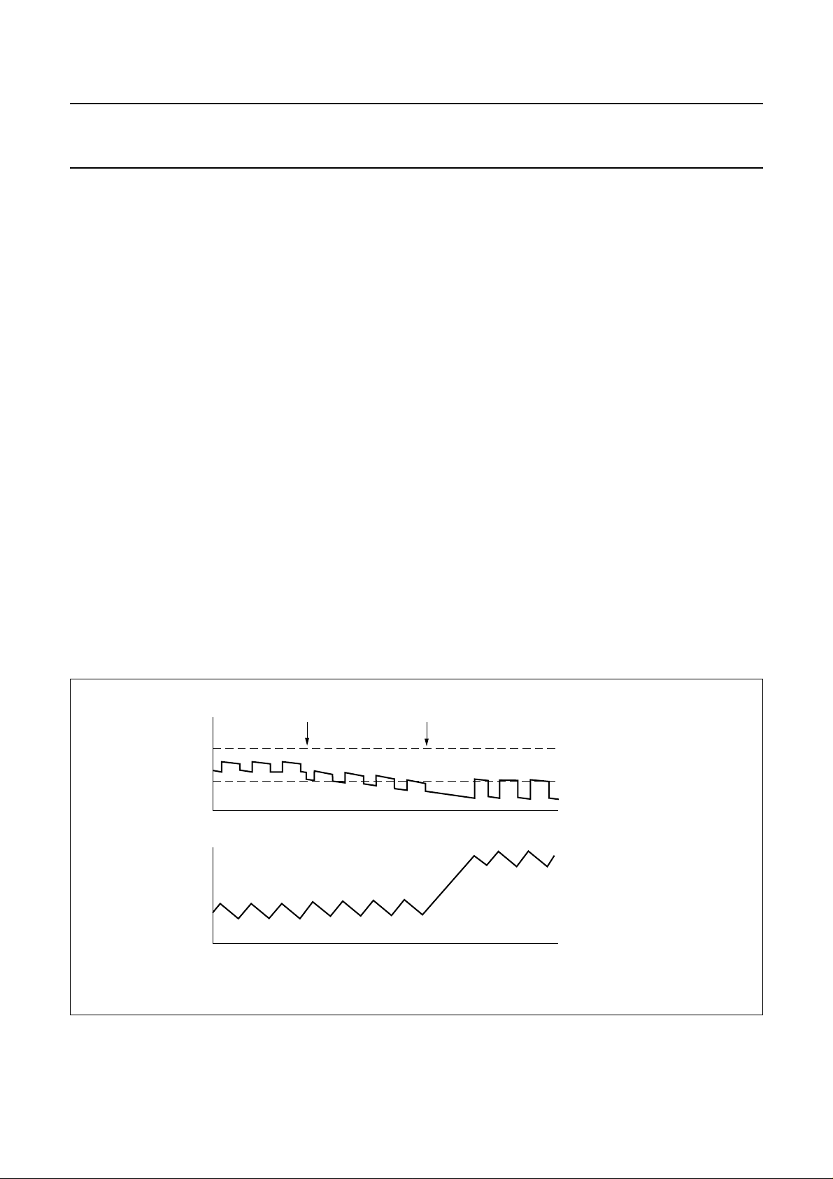
input to output ratio, see Fig.3.
handbook, halfpage
I
coil
0
VIN > V
OUT
down mode
VIN = V
OUT
stationary mode
Fig.3 Waveform of coilcurrentas function of I
and VIN to V
OUT
ratio.
VIN < V
up mode
PWM
PFM
OUT
MDB003
load
2003 Oct 13 5
Philips Semiconductors Preliminary specification
High efficiency auto-up/down
DC/DC converter
7.2.1 PWM
PWM results in minimum AC currents in the circuit
components and hence optimum efficiency, cost and
EMC. In this mode the output voltage is allowed to vary
between two predefined voltage levels. When the output
voltage stays within this so called window, switching
continues in a fixed pattern. When the output voltage
reaches one of the window borders, the digital controller
immediately reacts by adjusting the duty cycle and
inserting a current step in such a way that the output
voltage stays within the window with higher or lower
current capability. This approach enables very fast
reaction to load variations.
Figure 4 shows the TEA1211HN’s response to a sudden
load increase in case of up conversion. The upper trace
showstheoutput voltage.The rippleon topof theDC level
is a result of the current in the output capacitor, which
changes in sign twice per cycle, multiplied by the
capacitor’s internal Equivalent Series Resistance (ESR).
After eachramp-down of the inductorcurrent, or whenthe
ESR effect increases theoutput voltage, the TEA1211HN
determines what to do in the next cycle.As soon as more
load current is taken from the output the output voltage
starts to decay. When the output voltage becomes lower
than the low limit ofthe window, corrective action is taken
by a ramp-upof the inductor currentduring a much longer
time. As a result, the DC current level is increased and
TEA1211HN
normal PWM control can continue. The output voltage
(including ESR effect) is again within the predefined
window.
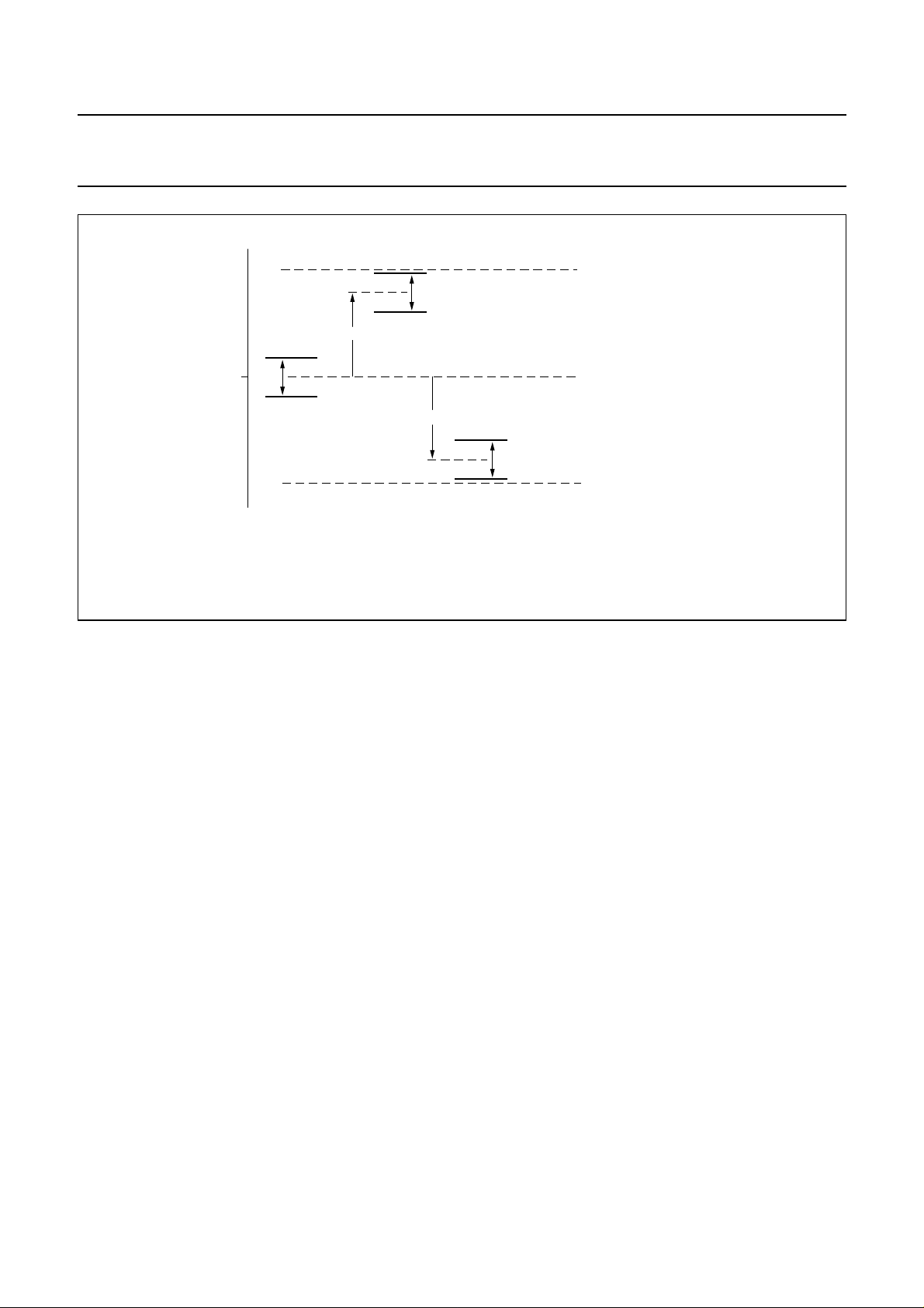
Figure 5 depicts the spread of theoutput voltage window.
Theabsolute valueismost dependentonspread,whilethe
actualwindowsize isnot affected.For onespecific device,
the output voltage will not vary more than 2 % typically.
7.2.2 PFM
In low output power situations, TEA1211HN will switch
over to PFM mode operation in case PWM-only mode is
not activated. In this mode charge is transferred from
battery to output in single pulses with a wait phase in
between. Regulation information from earlier PWM mode
operation is used. This results in optimum inductor peak
current levels in PFMmode,which are slightly larger than
the inductor ripple current in PWM mode. As a result, the
transition between PFM and PWM mode is optimal under
all circumstances. In PFM mode, the TEA1211HN
regulates the output voltage to the limits shown in Fig.5.
Depending on the VIN to V
decides for a 3- or 4-phase cycle, where the last phase is
the wait phase. When the inputvoltagealmost equals the
output voltage, one of the slopes of a 3-phase cycle
becomes weak. Then the charge, or the integral of its
pulse, is near to zero and no charge is transferred. In this
region the 4-phase cycle is used, (see Fig.3).
ratio the TEA1211HN
OUT
handbook, full pagewidth
V
OUT
I
load
load increase
start corrective action
Fig.4 Response to load increase in up-mode.
2003 Oct 13 6
time
time
high window limit
low window limit
MDB004
Philips Semiconductors Preliminary specification
High efficiency auto-up/down
DC/DC converter
handbook, full pagewidth
V
Vh= High window limit
Vl= Low window limit
OUT
(typ.)
2%
maximum positive spread of V
V
h
V
l
+4%
V
h
2%
V
l
−4%
maximum negative spread of V
FB
V
h
2%
V
l
upper specification limit
typical situation
lower specification limit
FB
TEA1211HN
MDB005
Fig.5 Spread of location of output voltage window.
7.2.3 SWITCHING SEQUENCE
Refer to Figures 1 and 3. In up-mode the cycle starts by
making P-down and N-up conducting in the first phase.
The second phase N-up opens and P-up starts
conducting. In down-mode the cycle startswithin the first
phase P-up and P-down conducting. The second phase
P-down opens and N-down starts conducting. In PFM
these twophases arefollowed bya thirdor waitphase that
opens all switches except for N-down, which is closed to
prevent the coil from floating.
The stationary mode or 4-phase cycle, which only occurs
in PFM, starts with in the first phase P-down and N-up
conducting. In the second phase P-down and P-up
conduct forming a short-cut from battery to output
capacitor. In the third phase P-up and N-down conduct.
The fourth or wait-phase again opens all switches except
for N-downwhich isclosed toprevent thecoil from floating.
7.3 Adjustable output voltage
Theoutput voltageof theTEA1211HN canbeset toa fixed
value by means of an external resistive divider. After
start-up through thisdivider, dynamic control ofthe output
voltage ismade possible by useof an I2C-bus. Theoutput
voltage can be programmed from 1.5 V to 5.5 V in
40 steps of 0.1 V each.Incase of Power Amplifiers (PAs)
for example the outputvoltage of the TEA1211HN can be
adjusted to the output power to be transmitted by the PA,
in order to obtain maximum system efficiency.
7.4 Start-up
If the input voltage exceeds the start voltage, the
TEA1211HN starts ramping up the voltage at the output
capacitor. Rampingstops when thetarget level, setby the
external resistors, is reached.
7.5 Under voltage lockout
As a result of too high load or disconnection of the input
power source, the input voltage can drop too low to
guarantee normal regulation. In that case, the device
switches to a shut-down mode stopping the switching
completely. Start-up is possible by crossing the start-up
level again.
7.6 Shut-down
When pin SHDWN is made HIGH, the converter disables
all switches except for N-down (see Fig.1) and power
consumption is reduced to a few µA. N-down is kept
conducting to prevent the coil from floating.
7.7 Power switches
The power switches in the IC are two N-type and two
P-type MOSFETs,having atypical pin-to-pin resistanceof
85 mΩ. The maximum continuous input/output current in
the switches is 1.7 A at 70 °C ambient temperature.
2003 Oct 13 7

Philips Semiconductors Preliminary specification
High efficiency auto-up/down
DC/DC converter
7.8 Synchronous rectification
For optimal efficiency over the whole load range,
synchronous rectifiers insidethe TEA1211HN ensure that
in PFM mode during the phase where the coil current is
decreasing, all inductor current will flow through the low
ohmic power MOSFETs. Special circuitry is included
which detects that the inductor current reaches zero.
Following this detection, the digital controller switches off
the power MOSFET and proceeds regulation. Negative
currents are thus prevented.
7.9 PWM-only mode
When pin SYNC/PWM is HIGH, the TEA1211HN will use
PWM regulation independent of the load applied. As a
result, the switching frequency does not vary over the
whole load range.
7.10 External synchronisation
If ahigh frequency clockis appliedto pin SYNC/PWM, the
switching frequency in PWM mode will be exactly that
frequency divided by 22. PFM mode is not possible if an
external clock is applied. The quiescent current of the
device increases when an external clock is applied.
In case no external synchronisation is necessary and the
PWM-only option is not used, pin SYNC/PWM must be
connected to ground.
7.11 Current limiter
If the peak input current of the TEA1211HN exceeds its
limit in PWM mode, current ramping is stopped
immediately, andthe nextswitching phase isentered. The
TEA1211HN
current limitation protects the IC against overload
conditions, inductor saturation, etc. The current limit level
is user defined by the external resistor which must be
connected between pin ILIM and pin GND.
2
7.12 I
The serial interface of the TEA1211HN is the I2C-bus.
A detailed description of the I2C-bus specification,
including applications, is given in the brochure:
I2C-bus and how to use it”
7.12.1 C
The I2C-bus is for bidirectional, two-line communication
between different ICs or modules. The two lines are a
Serial Dataline (SDA)and a SerialClock Line(SCL). Both
lines must be connected to a positive supply via a pull-up
resistor (for best efficiency it is advised to use the input
voltage of the convertor). Data transfer may be initiated
only when the bus is not busy. In bus configurations with
ICs ondifferent supply voltages, thepull-up resistors shall
be connected to the highest supply voltage. The I2C-bus
supportsincremental addressing.This enablesthe system
controller to read or write multiple registers in only one
I2C-bus action. The TEA1211HN supports the I2C-bus up
to 400 kbit/s.
The I2C-bus system configuration is shown in Fig.6.
A device generating a message is a transmitter, a device
receivinga messageis areceiver. Thedevicethatcontrols
the message is the master and the devices which are
controlled by the master are theslaves. The TEA1211HN
is a slave only device.
C-bus serial interface
, order no. 9398 393 40011.
HARACTERISTICS OF THE I
2
C-BUS
“The
handbook, full pagewidth
SDA
SCL
MASTER
TRANSMITTER /
RECEIVER
SLAVE
RECEIVER
TRANSMITTER /
RECEIVER
Fig.6 I2C-bus system configuration.
2003 Oct 13 8
SLAVE
MASTER
TRANSMITTER
MASTER
TRANSMITTER /
RECEIVER
MDB006

Philips Semiconductors Preliminary specification
High efficiency auto-up/down
TEA1211HN
DC/DC converter
7.12.2 START AND STOP CONDITIONS
Both data and clock lines remain HIGH when the bus is not busy. A HIGH-to-LOW transition of the data line, while the
clock is HIGH is definedas the START condition (S). A LOW-to-HIGH transition of thedata line while the clock is HIGH
is defined as the STOP condition (P) (see Fig.7).
handbook, full pagewidth
7.12.3 BIT TRANSFER
SDA
SCL
START condition
S
P
STOP condition
Fig.7 START and STOP conditions on the I2C-bus.
SDA
SCL
MDB007
One databit is transferredduring each clockpulse. The dataon theSDAline mustremain stable duringthe HIGH period
of the clock pulse as changes in the data line at this time will be interpreted as a control signal (see Fig.8).
handbook, full pagewidth
SDA
SCL
data line
stable;
data valid
change
of data
allowed
MDB008
Fig.8 Bit transfer on the I2C-bus.
7.12.4 ACKNOWLEDGE
The numberof databytes transferredbetween the STARTand STOPconditions fromtransmitterto receiveris unlimited.
Each byte of eight bits is followedbyan acknowledge bit. The acknowledge bit is a HIGH level signal put on the busby
the transmitter during which time the receiver generates an extra acknowledge related clock pulse.
A slave receiver which is addressed must generate an acknowledge after the reception of each byte. Also a master
receiver must generate an acknowledge after the reception of each byte that has been clocked out of the slave
transmitter (see Fig.9).
The device that acknowledgesmust pull down the SDA lineduring the acknowledge clock pulse, so thatthe SDA line is
stable LOW duringthe HIGH period of theacknowledge related clock pulse (set-upand hold times must beconsidered).
A master receiver must signal an end of data to the transmitter by not generating an acknowledge on the last byte that
has been clocked out of the slave. In this event the transmitter must leave the data line HIGH to enable the master to
generate a STOP condition.
2003 Oct 13 9

Philips Semiconductors Preliminary specification
High efficiency auto-up/down
DC/DC converter
handbook, full pagewidth
DATA OUTPUT
BY SLAVE
TRANSMITTER
DATA OUTPUT
BY SLAVE
RECEIVER
SCL FROM
MASTER
TRANSMITTER
S
START
condition
Fig.9 Acknowledge on the I2C-bus.
not acknowledge
acknowledge
acknowledgement
TEA1211HN
9821
clock pulse for
MDB009
7.12.5 I2C-BUS PROTOCOL
7.12.5.1 Addressing
Before any data is transmitted on the I2C-bus, the device which should respond is addressed first. The addressing is
always carried out with the first byte transmitted after the start procedure. The (slave) address of the TEA1211HN is
0001 0000 (10h). The subaddress (or word address) is 0000 0000 (00h).
The TEA1211HN acts as a slave receiver only. Therefore the clock signal SCL is only an input signal. The data signal
SDA is a bidirectional line, enabling the TEA1211HN to send an acknowledge.
7.12.5.2 Data
The data consists of one byte, addressing the 40 voltage steps as explained in Tables 1 and 2.
Table 1 Data byte
SUBADDRESS BIT 7 BIT 6 BIT 5 BIT 4 BIT 3 BIT 2 BIT 2 BIT 0
00h 0 0 CVLVL5 CVLVL4 CVLVL3 CVLVL2 CVLVL1 CVLVL0
Table 2 Translation data byte to voltage level
SUBADDRESS NAME
SIZE
(BIT)
STEP NUMBER
MIN. MAX.
MIN. (V)
STEP
(V)
MAX. (V)
00h CVLVL 6 0 40 1.5 0.1 5.5
2003 Oct 13 10

Philips Semiconductors Preliminary specification
High efficiency auto-up/down
TEA1211HN
DC/DC converter
7.12.5.3 Write Cycle
The I2C-bus configuration forthe different TEA1211HN write cycles isshown in Fig.10. The word addressis an eight bit
value that defines which register is to be accessed next.
handbook, full pagewidth
S = START condition.
P = STOP condition.
acknowledgement
from slave
R/W
WORD ADDRESS
ASLAVE ADDRESS A ADATA
S
0
Fig.10 Master transmits to slave receiver (write mode).
acknowledgement
from slave
acknowledgement
from slave
n bytes
auto increment
memory word address
P
MDB010
8 LIMITING VALUES
SYMBOL PARAMETER CONDITIONS MIN. MAX. UNIT
V
n
voltage on any pin with respect
to GND
P
tot
T
j
T
amb
T
stg
V
esd
total internal power dissipation − 1000 mW
junction temperature −40 +150 °C
ambient temperature −40 +85 °C
storage temperature −40 +125 °C
electrostatic discharge voltage
shut-down mode −0.5 +6.0 V
operational mode −0.5 +5.5 V
pins LXA note 1 −±800 V
note 2 −±200 V
all other pins JEDEC Class II; note 1 −±2000 V
JEDEC Class II; note 2 −±200 V
Notes
1. Human Body Model: equivalent to discharging a 100 pF capacitor via a 1.5 kΩ resistor.
2. Machine Model: equivalent to discharging a 200 pF capacitor via a 0.75 µH series inductor.
9 THERMAL CHARACTERISTICS
SYMBOL PARAMETER CONDITIONS VALUE UNIT
R
th(j-a)
thermal resistancefrom junction
to ambient
mounted on dedicated PCB in
free air
35 K/W
2003 Oct 13 11

Philips Semiconductors Preliminary specification
High efficiency auto-up/down
TEA1211HN
DC/DC converter
10 CHARACTERISTICS
T
= −40 to +85 °C; all voltages with respect to ground; positive currents flow into theIC; unless otherwise specified.
amb
SYMBOL PARAMETER CONDITIONS MIN. TYP. MAX. UNIT
Voltage levels
V
OUT
V
IN(start)
V
IN
V
IN(uvlo)
V
FB
V
OUT(wdw)
Current levels
I
q
I
shdwn
∆I
lim
I
max
Power MOSFETs; note 2
R
DS(on)(N)
R
DS(on)(P)
R
DS(on)(P-up)
Timing
f
sw
f
sync
Digital levels: pins SYNC/PWM, SHDWN, SCL and SDA
V
IL
V
IH
Temperature
T
amb
T
max
output voltage 1.50 − 5.50 V
start voltage V
input voltage V
under voltage lockout level − V
I
load
OUT
= 3.5 V;
< 100 mA
2.45 2.55 2.65 V
IN(start)
− 5.50 V
− 0.15 − V
IN(start)
feedback voltage level 1.20 1.25 1.30 V
output voltage window as
percentage of V
OUT
PWM mode 1.5 2.0 3.0 %
quiescent current no load − 100 −µA
current in shut-down mode − <1 2 µA
current limit deviation I
maximum continuous
= 1 A; note 1 −30 − +30 %
lim
T
<70°C −− 1.7 A
amb
input/output current
pin-to-pin resistance NFETs VIN= 3.5 V − 65 85 mΩ
pin-to-pin resistance PFETs VIN= 3.5 V − 65 85 mΩ
pin-to-pin resistance P-up
V
= 1.5 V − 100 135 mΩ
OUT
FET between pins LXB and
OUT
switching frequency PWM mode 450 600 750 kHz
synchronization input
4.5 13 20 MHz
frequency
LOW-level input voltage 0 − 0.4 V
HIGH-level input voltage note 3 0.6 × VIN− VIN+ 0.3 V
ambient temperature −40 +25 +85 °C
internal cut-off temperature 120 135 150 °C
Notes
1. Current limit level is defined by the external R
2. Measured at T
amb
=25°C.
resistor, see Chapter 11.
lim
3. To avoid additional supply current, it is advised to use HIGH levels not lower than VIN− 0.5 V.
2003 Oct 13 12

Philips Semiconductors Preliminary specification
High efficiency auto-up/down
DC/DC converter
11 APPLICATION INFORMATION
11.1 Typical Li-Ion, 2- or 3-cell application with I
handbook, full pagewidth
D1 D2
VIN =
2.55 to 5.5 V
battery
C
100 µF
123 4 10 11 14 15 21 22 24
31
32
IN
12 13 29 28 30 5 7 9 16 18 20
SCL
SYNC/
PWM
SDA SHDWN
2
C-bus programming
L1
10 µH
LXA LXB
TEA1211HN
ILIM
R
lim
1 kΩ
TEA1211HN
V
= 3.3 V
R1
120 kΩ
R2
75 kΩ
OUT
C
OUT
100 µF
MDB011
OUTIN
26
25
23
FB
27
GND
The combination of the feedback resistors R1 and R2 in parallel should be approximately 50 kΩ.
D1 and D2 are Schottky diodes
The battery can be a one cell Li-Ion, two cell Alkaline or three cell NiCd/NiMH/Alkaline.
If the I2C-bus interface isused for programmingthe output voltage, the SCLand SDA linesmust be connectedto a positivesupply via pull-up resistors
(see Section 7.12.1). If the I
Note the VIH-level (see Chapter 10).
Pins should never be left open-circuit.
No external clock is applied.
2
C-bus interface is not used, connect pins SCL and SDA to ground.
Fig.11 The TEA1211HN in a typical auto-up/down converter application.
2003 Oct 13 13

Philips Semiconductors Preliminary specification
High efficiency auto-up/down
DC/DC converter
100
handbook, full pagewidth
(1)
η
(2)
(%)
(3)
80
60
40
20
0
(4)
(5)
1 10 100 1000
I
load
TEA1211HN
MDB013
(mA)
V
= 3.3 V.
OUT
L1=10µH, TDK SLF7032 series.
(1) VIN= 2.7 V.
(2) VIN= 3.3 V.
(3) VIN= 3.6 V.
(4) VIN= 4.2 V
(5) VIN= 4.5 V.
Fig.12 Efficiency as a function of load current.
2003 Oct 13 14

Philips Semiconductors Preliminary specification
High efficiency auto-up/down
DC/DC converter
100
handbook, full pagewidth
η
(%)
(1)
(2)
(3)
80
60
40
20
0
2.50 3.00 3.50 4.00 4.50
(4)
(5)
TEA1211HN
MDB012
V
(V)
IN
V
= 3.3 V.
OUT
L1=10µH, TDK SLF7032 series.
(1) I
= 1000 mA.
OUT
(2) I
= 500 mA.
OUT
(3) I
= 100 mA.
OUT
(4) I
=10mA.
OUT
(5) I
= 1 mA.
OUT
Fig.13 Efficiency as a function of input voltage.
2003 Oct 13 15

Philips Semiconductors Preliminary specification
High efficiency auto-up/down
TEA1211HN
DC/DC converter
11.2 Component selection
11.2.1 INDUCTOR
The inductor should have a low Equivalent Series Resistance (ESR) to reduce losses and the inductor must be able to
handle the peak currents without saturating.
Table 3 Inductor selection information
COMPONENT VALUE TYPE SUPPLIER
L1 6.8 µH DO3316-682 Coilcraft
L1 10 µH SLF7032T-100M1R4 TDK
11.2.2 CAPACITORS
For theoutputcapacitor the ESRiscritical. The outputvoltageripple is determined bythe product of thecurrent through
the output capacitor and its ESR. The lower the ESR, the smaller the ripple. However, an ESR less than 80 mΩ could
result in unstable operation.
Table 4 Input and output capacitor selection information
COMPONENT VALUE TYPE SUPPLIER
, C
C
IN
OUT
100 µF/10 V TPS-series AVX
594D-series Vishay/Sprague
If the I2C-bus interface is used to program the output voltage, use a larger input capacitor to prevent the under voltage
lockout level being triggered by large current peaks drawn from this capacitor.
2
Table 5 Input capacitor selection information, when I
COMPONENT VALUE TYPE SUPPLIER
C
(I2C-bus used) 220 to 470 µF/10 V TPS-series AVX
IN
11.2.3 SCHOTTKY DIODES
The Schottky diodes provide a lower voltage drop during the break-before-make time of the internal power FETs. It is
advised to use Schottky diodes with fast recovery times.
Table 6 Schottky selection information
COMPONENT TYPE SUPPLIER
D1, D2 PRLL5819 Philips
C-bus is used
594D-series Vishay/Sprague
2003 Oct 13 16

Philips Semiconductors Preliminary specification
High efficiency auto-up/down
TEA1211HN
DC/DC converter
11.2.4 FEEDBACK RESISTORS
The fixedoutput voltage can beset with thefeedback resistors R1 andR2 (see Fig.11).Even in case I2C-bus isused for
programming the output voltage, these external resistors are required for start-up. The ratio of the resistors can be
V
calculated by: , with V
R1
------R2
The two resistors in parallel should have a value of approximately 50 kΩ:
1
+
-------
-------
R1
R2
11.2.5 C
1
1
≈
---------------50 kΩ
URRENT LIMITER
The maximum input peak current can be set by the current limiter as follows:
R
lim
-----------------------------I
IN(peak)(max)
1250
=
Remark. The output current is not limited: in down conversion, the output current will be higher than the input current,
but the maximum continuous output current is not allowed to exceed 1.7 A (RMS) at 70 °C.
------------V
Ω
OUT
ref
1–=
ref=VFB
(see Chapter 10).
Table 7 Resistor selection information
COMPONENT VALUE TYPE TOLERANCE
R1, R2 V
R
lim
dependent SMD 1 %
OUT
I
dependent SMD 1 %
lim
2003 Oct 13 17

Philips Semiconductors Preliminary specification
High efficiency auto-up/down
DC/DC converter
12 PACKAGE OUTLINE
HVQFN32: plastic thermal enhanced very thin quad flat package; no leads;
32 terminals; body 5 x 5 x 0.85 mm
A
D
terminal 1
index area
B
E
TEA1211HN
SOT617-3
A
A
1
detail X
c
e
1
e
916
L
8
E
h
1
terminal 1
index area
DIMENSIONS (mm are the original dimensions)
(1)
A
UNIT
mm
Note
1. Plastic or metal protrusions of 0.075 mm maximum per side are not included.
max.
A
0.05
0.00
1
32 25
(1)
c
b
0.30
0.18
0.2
D
5.1
4.9
1/2 e
b
17
e
1/2 e
24
D
h
0 2.5 5 mm
scale
(1)
E
5.1
4.9
E
3.75
3.45
h
0.51
D
3.75
3.45
h
w
e
3.5
C
v
M
ACCB
M
e
2
e
3.5
L
2
0.5
0.3
1
y
C
1
0.1v0.05
w
ye
0.05 0.1
y
X
y
1
OUTLINE
VERSION
SOT617-3 MO-220- - - - - -
IEC JEDEC JEITA
REFERENCES
2003 Oct 13 18
EUROPEAN
PROJECTION
ISSUE DATE
02-04-18
02-10-22

Philips Semiconductors Preliminary specification
High efficiency auto-up/down
DC/DC converter
13 SOLDERING
13.1 Introduction to soldering surface mount
packages
Thistext givesa verybriefinsight toa complextechnology.
A more in-depth account of soldering ICs can be found in
our
“Data Handbook IC26; Integrated Circuit Packages”
(document order number 9398 652 90011).
There is no soldering method that is ideal for all surface
mount IC packages. Wave soldering can still be used for
certainsurface mountICs, butitis notsuitable forfinepitch
SMDs. In these situations reflow soldering is
recommended.
13.2 Reflow soldering
Reflow soldering requires solder paste (a suspension of
fine solder particles, flux and binding agent) to be applied
tothe printed-circuitboard byscreen printing,stencilling or
pressure-syringe dispensing before package placement.
Driven by legislation and environmental forces the
worldwide use of lead-free solder pastes is increasing.
Several methods exist for reflowing; for example,
convection or convection/infrared heating in a conveyor
type oven. Throughput times (preheating, soldering and
cooling) vary between 100 and 200 seconds depending
on heating method.
Typical reflow peak temperatures range from
215 to 270 °C depending on solder paste material. The
top-surface temperature of the packages should
preferably be kept:
• below 220 °C (SnPbprocess) or below 245 °C (Pb-free
process)
– for all BGA and SSOP-T packages
– for packages with a thickness≥2.5mm
– for packages with a thickness <2.5 mm and a
volume ≥ 350 mm3 so called thick/large packages.
• below 235 °C (SnPbprocess) or below 260 °C (Pb-free
process) for packages witha thickness < 2.5 mm and a
volume < 350 mm3 so called small/thin packages.
Moisture sensitivity precautions, as indicated on packing,
must be respected at all times.
13.3 Wave soldering
Conventional single wave soldering is not recommended
forsurface mountdevices (SMDs)orprinted-circuit boards
TEA1211HN
with a high component density, as solder bridging and
non-wetting can present major problems.
To overcome these problems the double-wave soldering
method was specifically developed.
If wave soldering isusedthe following conditions must be
observed for optimal results:
• Use a double-wave soldering method comprising a
turbulent wavewith high upward pressurefollowed by a
smooth laminar wave.
• For packages with leads on two sides and a pitch (e):
– larger than or equal to 1.27mm, the footprint
longitudinal axis is preferred to be parallel to the
transport direction of the printed-circuit board;
– smaller than 1.27mm, the footprint longitudinal axis
must be parallel to the transport direction of the
printed-circuit board.
The footprint must incorporate solder thieves at the
downstream end.
• Forpackages withleads onfoursides, thefootprint must
be placedata 45° angle tothe transport direction ofthe
printed-circuit board. The footprint must incorporate
solder thieves downstream and at the side corners.
During placementand beforesoldering, the packagemust
be fixed with a droplet of adhesive. The adhesive can be
applied by screen printing, pin transfer or syringe
dispensing. The package can be soldered after the
adhesive is cured.
Typical dwell time of the leads in the wave ranges from
3 to 4 seconds at 250 °C or 265 °C, depending on solder
material applied, SnPb or Pb-free respectively.
A mildly-activated flux will eliminate the need for removal
of corrosive residues in most applications.
13.4 Manual soldering
Fix the component by first soldering two
diagonally-opposite end leads.Use a low voltage(24 V or
less) soldering iron applied to the flat part of the lead.
Contact time must be limited to 10 seconds at up to
300 °C.
When using a dedicated tool, all other leads can be
soldered in one operation within 2 to 5 seconds between
270 and 320 °C.
2003 Oct 13 19

Philips Semiconductors Preliminary specification
High efficiency auto-up/down
TEA1211HN
DC/DC converter
13.5 Suitability of surface mount IC packages for wave and reflow soldering methods
PACKAGE
BGA, LBGA, LFBGA, SQFP, SSOP-T
DHVQFN, HBCC, HBGA, HLQFP, HSQFP, HSOP, HTQFP,
(1)
(3)
, TFBGA, VFBGA not suitable suitable
not suitable
HTSSOP, HVQFN, HVSON, SMS
(5)
PLCC
, SO, SOJ suitable suitable
LQFP, QFP, TQFP not recommended
SSOP, TSSOP, VSO, VSSOP not recommended
(8)
PMFP
not suitable not suitable
Notes
1. Formore detailedinformation onthe BGApackages referto the
“(LF)BGAApplication Note
from your Philips Semiconductors sales office.
2. All surface mount (SMD) packages are moisture sensitive. Depending upon the moisture content, the maximum
temperature (with respect to time) and body size of the package, there is a risk that internal or external package
cracks may occur due to vaporizationof the moisture in them (the so called popcorn effect). For details,refer to the
Drypack information in the
“Data Handbook IC26; Integrated Circuit Packages; Section: Packing Methods”
3. These transparent plastic packages are extremely sensitive to reflow soldering conditions and must on no account
be processedthrough more thanone soldering cycleor subjected toinfrared reflow soldering withpeak temperature
exceeding 217 °C ± 10 °C measured in the atmosphere of the reflow oven. The package body peak temperature
must be kept as low as possible.
4. These packages are not suitable for wave soldering. On versions with the heatsink on the bottom side, the solder
cannot penetrate between the printed-circuit boardandthe heatsink. On versions with the heatsink on the top side,
the solder might be deposited on the heatsink surface.
5. If wave soldering is considered, then the package must be placed at a 45° angle to the solder wave direction.
The package footprint must incorporate solder thieves downstream and at the side corners.
6. Wave solderingis suitable forLQFP, TQFP andQFP packages with apitch (e) largerthan 0.8 mm; itis definitely not
suitable for packages with a pitch (e) equal to or smaller than 0.65 mm.
7. Wave soldering is suitable for SSOP, TSSOP, VSO and VSSOP packages with a pitch (e) equal to or larger than
0.65 mm; it is definitely not suitable for packages with a pitch (e) equal to or smaller than 0.5 mm.
8. Hot bar or manual soldering is suitable for PMFP packages.
SOLDERING METHOD
WAVE REFLOW
(4)
(5)(6)
(7)
suitable
suitable
suitable
”(AN01026); ordera copy
(2)
.
2003 Oct 13 20

Philips Semiconductors Preliminary specification
High efficiency auto-up/down
TEA1211HN
DC/DC converter
14 DATA SHEET STATUS
LEVEL
I Objective data Development This data sheet contains data from the objective specification for product
II Preliminary data Qualification This data sheet contains data from the preliminary specification.
III Product data Production This data sheet contains data from the product specification. Philips
Notes
1. Please consult the most recently issued data sheet before initiating or completing a design.
2. The product status of the device(s) described in this data sheet may have changed since this data sheet was
published. The latest information is available on the Internet at URL http://www.semiconductors.philips.com.
3. For datasheets describing multipletype numbers,the highest-level productstatus determines thedata sheetstatus.
DATA SHEET
STATUS
(1)
PRODUCT
STATUS
(2)(3)
development. Philips Semiconductors reserves the right to change the
specification in any manner without notice.
Supplementary data will be published at a later date. Philips
Semiconductors reserves the right to change the specification without
notice, in order to improve the design and supply the best possible
product.
Semiconductors reserves the right to make changes at any time in order
to improve the design, manufacturing and supply. Relevant changes will
be communicated via a Customer Product/Process Change Notification
(CPCN).
DEFINITION
15 DEFINITIONS
Short-form specification The data in a short-form
specification is extracted from a full data sheet with the
same type number and title. For detailed information see
the relevant data sheet or data handbook.
Limiting valuesdefinition Limitingvalues givenarein
accordance with the Absolute Maximum Rating System
(IEC 60134). Stress above one or more of the limiting
values may cause permanent damage to the device.
These are stress ratings only and operation of the device
atthese orat anyother conditionsabovethose givenin the
Characteristics sectionsof the specification isnot implied.
Exposure to limiting values for extended periods may
affect device reliability.
Application information Applications that are
described herein for any of these products are for
illustrative purposes only. Philips Semiconductors make
norepresentation orwarrantythat suchapplications willbe
suitable for the specified use without further testing or
modification.
16 DISCLAIMERS
Life support applications These products are not
designed for use in life support appliances, devices, or
systems where malfunction of these products can
reasonably beexpected toresult inpersonal injury.Philips
Semiconductorscustomers usingorselling theseproducts
for use in such applications do so at their own risk and
agree to fully indemnify Philips Semiconductors for any
damages resulting from such application.
Right to make changes Philips Semiconductors
reserves the right to make changes in the products including circuits, standard cells, and/or software described or contained herein in order to improve design
and/or performance.When theproduct is infull production
(status ‘Production’), relevant changes will be
communicated via a Customer Product/Process Change
Notification (CPCN). Philips Semiconductorsassumes no
responsibility or liability for the use of any of these
products, conveys no licence or title under any patent,
copyright, or mask work right to these products, and
makes no representations or warranties that these
products are free from patent, copyright, or mask work
right infringement, unless otherwise specified.
2003 Oct 13 21

Philips Semiconductors Preliminary specification
High efficiency auto-up/down
DC/DC converter
17 PURCHASE OF PHILIPS I2C COMPONENTS
Purchase of Philips I2C components conveys a license under the Philips’ I2C patent to use the
components inthe I2C systemprovided the system conformsto the I2C specificationdefined by
Philips. This specification can be ordered using the code 9398 393 40011.
TEA1211HN
2003 Oct 13 22

Philips Semiconductors – a w orldwide compan y
Contact information
For additional information please visit http://www.semiconductors.philips.com. Fax: +31 40 27 24825
For sales offices addresses send e-mail to: sales.addresses@www.semiconductors.philips.com.
© Koninklijke Philips Electronics N.V. 2003
All rights are reserved. Reproduction in whole or in part is prohibited without the prior written consent of the copyright owner.
The information presented in this document does not formpart ofany quotation or contract, is believed to be accurateand reliableand may be changed
without notice. No liability will be accepted by the publisher for any consequence of its use. Publication thereof does not convey nor imply any license
under patent- or other industrial or intellectual property rights.
Printed in The Netherlands R54/02/pp23 Date of release: 2003 Oct 13 Document order number: 9397 750 12174
SCA75
 Loading...