

Page 1
TEA1024/ TEA1124
Zero Voltage Switch with Fixed Ramp
Description
The monolithic integrated bipolar circuit, TEA1024/
TEA1124 is a zero voltage switch for triac control in
domestic equipments. It offers not only the control of a
triac in zero crossing mode but also the possibility of
power control. This is why the IC contains a mains
Features
D
Direct supply from the mains
D
Definite IC switching characteristics
D
Very few external components
D
Full wave drive – no dc component in the load circuit
D
Current consumption ≤ 1.5 mA
synchronized ramp generator with 640 ms (1280 ms)
duration (50 Hz). It is suitable for a typical load of 750 W
(1000 W) meeting the Flicker Standard. (values in
brackets relate to TEA1124.)
D
Simple power control
D
Integrated ramp generator
D
Reference voltage variable by external resistance
D
Pulse position optimization
D
Output short circuit protected
Block Diagram
95 10871
1
56 k
W
W
Protection
2
43 k
W
min.
100 k
max.
Ramp generator
TEA 1024 – 640 ms
TEA 1124 – 1280 ms
Comparator
+
–
NC
Package: DIP8
R
390 k
W
Sync. logic Supply
3 8
2
(R
sync
7 4
NC
MT2
MT1
L
V
=
M
230 V ~
N
D
)
1
R
1
amplifier
22 kW/
2 W
Pulse
1N4007
Load
1000 W
C
100 mF
1
16 V
6
5
R
68
TIC
236N
G
W
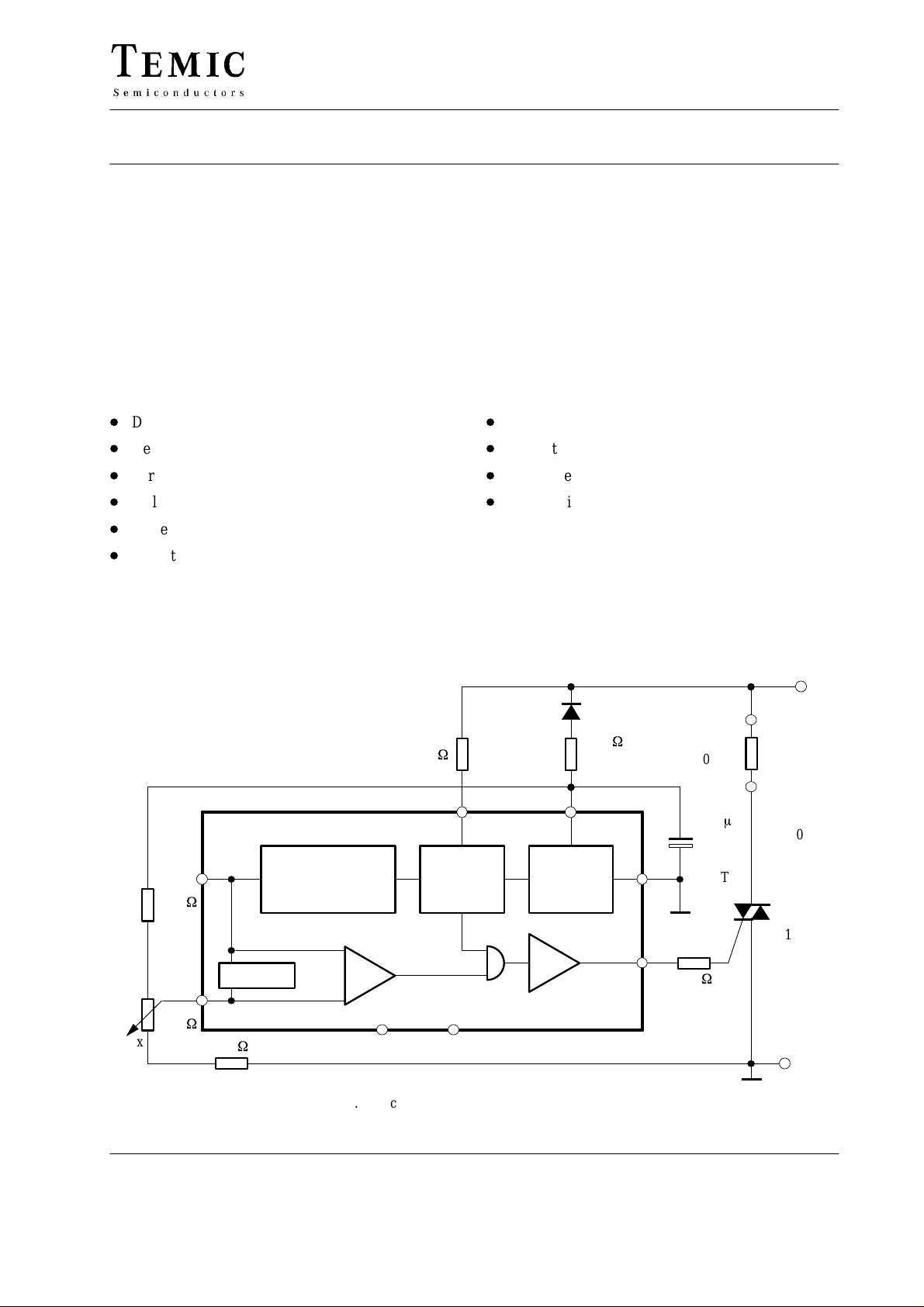
Figure 1. Typical block diagram – open loop power control
TELEFUNKEN Semiconductors
Rev . A1, 24-May-96
1 (8)
Page 2
TEA1024/ TEA1124
Power Supply and its Limitations
The voltage limitation contained in the IC allows it to be
powered from mains via series resistance R
fying diode D
The capacitor C
between Pin 6 (+ Pol/ă) and Pin 4 (–VS).
1
smooths the supply voltage
1
and recti–
1
(see figure 1).
An internal temperature-compensated limiting circuit
protects the module from random peaks of voltage on the
mains, and delivers a defined reference voltage during the
negative half-cycle.
Synchronization
Full-Wave Logic
The full-wave logic ensures that only pairs of pulses can
be released, and that these always begin with the positive
dv/dt. The load is thus switched on for a minimum of one
complete mains cycle. This means that the triac receives
a minimum of two driving pulses, so that the unwanted
d.c. component in the load circuit is definitely eliminated.
Pulse Amplifier
The pulse amplifier connected to the output of the fullwave logic circuit, is proof against continuos
short-circuits, and delivers negative output pulses of typ.
75 mA, via an integrated limiting resistance, to Pin 5.
Ramp Generator (Figures 3, 4)
Ramp voltage which is generated in the IC is available not
only at reference Pin 1, but also at the non-inverted input
of the comparator.
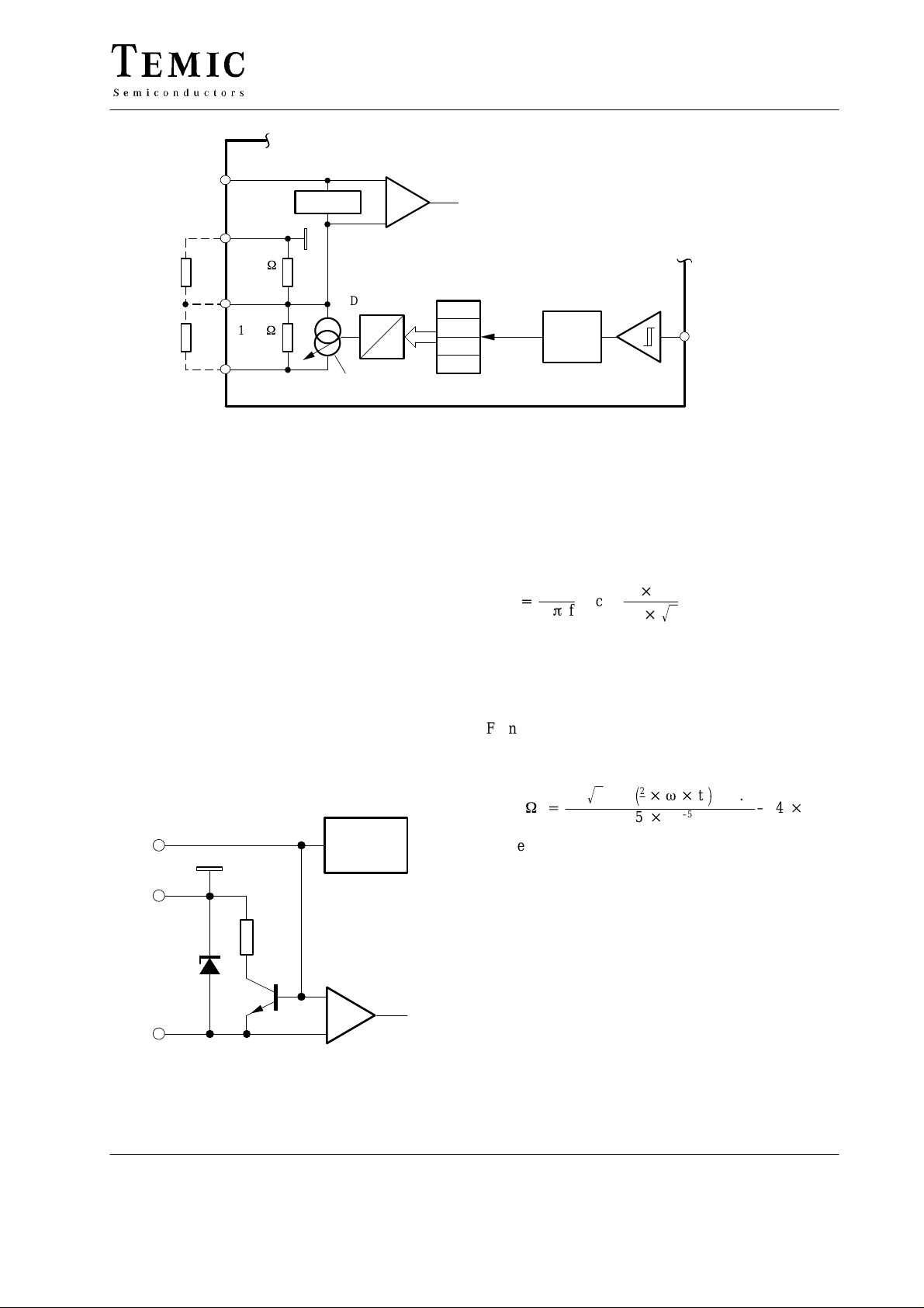
The current sink which is controlled by D/A converter
influences the internal reference voltage at Pin 1 specified
by voltage divider. The current sink is turned-off in the
reset state of the D/A converter so that the voltage at Pin 1
is primarily specified via the internal voltage divider
(ramp starting voltage).
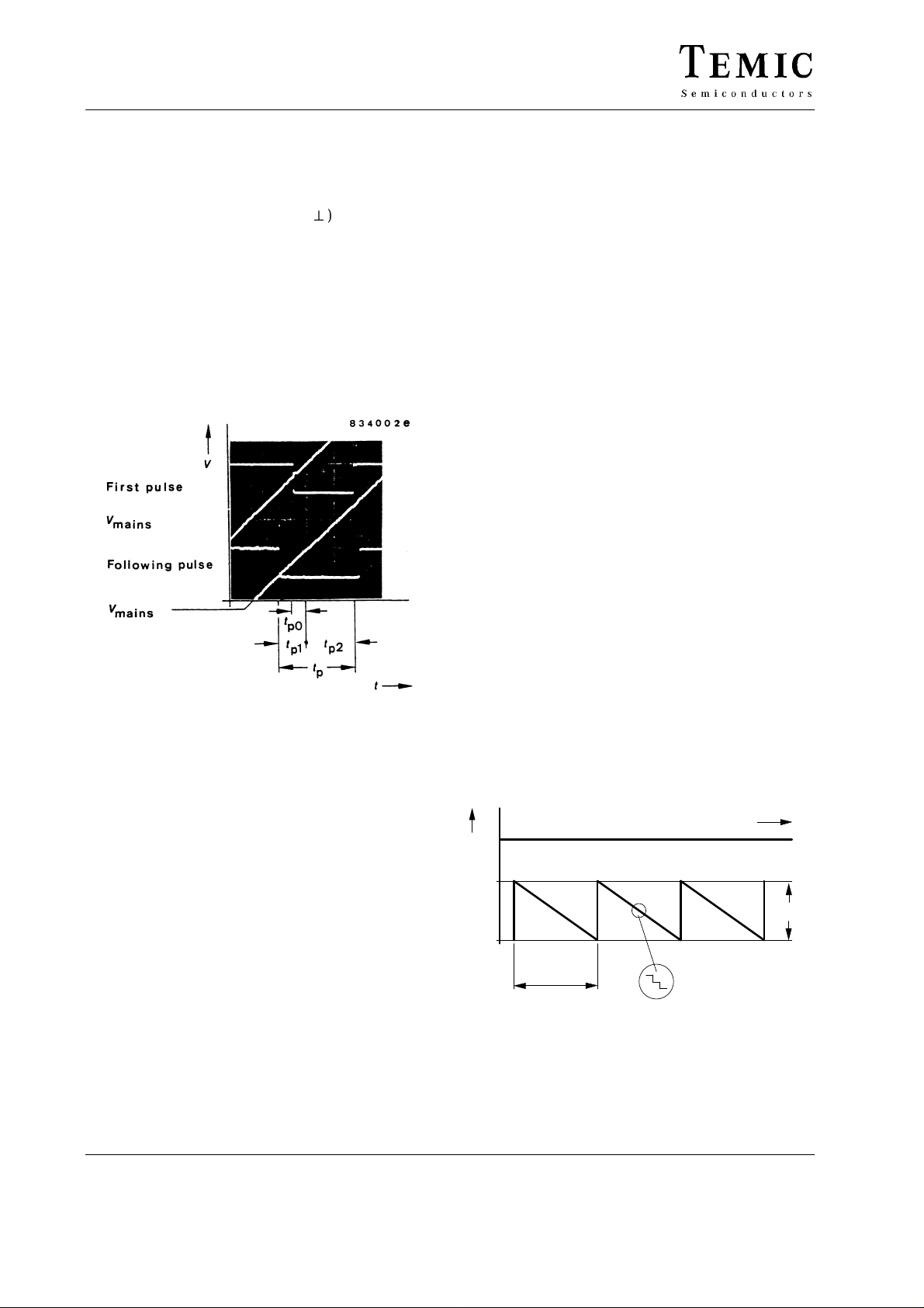
Figure 2. Pulse position optimization
The logic function is synchronized by means of a separate
resistance R
connected between Pin 7 and phase
2
(voltage-synchronization). The width of the pulse can be
varied between wide limits by choice of R
. The larger
sync
the value chosen, the wider the output pulse is on Pin 5.
Automatic optimization of the phase of the pulse is
necessary, since the latching current of the triac exceeds
the steady current by a factor of 3.
The phase of the pulse is chosen so that ca. 1/3 of the pulse
width appears before the transition through null and 2/3
after it (see electrical characteristics and figure 2).
In order to avoid phase-clipping after the switch-on the
first third of the first pulse is automatically suppressed.
In the maximum state of the 4 stage (5 stage – TEA1124)
D/A converter, the current sink overtakes the maximum
current, whereby the ramp’s final (end) voltage has
reached. External resistance R
, Ry shown in figure 4 are
x
in position to influence the initial ramp voltage as well as
the ramp amplitude. If the external resistances ratio R
is the same as that of the internal ratio, the ramp
R
y
voltage at the beginning remains maintained (constant),
only the amplitude is compressed.
t
V
1
–1.3 V
2.2 V
–3.8 V
T= 640 ms
(T= 1280 ms)
95 11410
Figure 3. Ramp diagram without external circuit
16 stage ramp
,
x
2 (8)
TELEFUNKEN Semiconductors
Rev . A1, 24-May-96
Page 3
GND
R
R
–V
TEA1024/ TEA1124
2
Protection
6
50 k
1
150 k
4
W
W
Current sink
Figure 4. Principle diagram – Generation and evaluation of ramp
x
y
S
–
+
D/A converter
A
D
4 stage
ripple counter
3
2
2
2
1
2
0
2
Period
20 ms
(40 ms)
Divider
1:2
(1:4)
7
Sync (50 Hz)
95 11411
Period
1. The time required for one complete cycle of a regular.
repeating signal, function, or series of emends.
2. The tune between two consecutive transients of the
pointer or indicating means of an electrical indicating
instrument in the same disdain the rest position.
Something called periodic fine.
Comparator
The comparison of set value and measured value is
carried out via the two comparator inputs Pin 1 and Pin 2.
Here Pin 2 is the inverting input and has a circuit protecting it against interference spikes. Figure 5 shows the
protective circuit of the comparator. Pin 1 is the noninverting input.
1
6
GND
R
Z
Ramp
generator
Firing Pulse Width (Figures 6, 7)
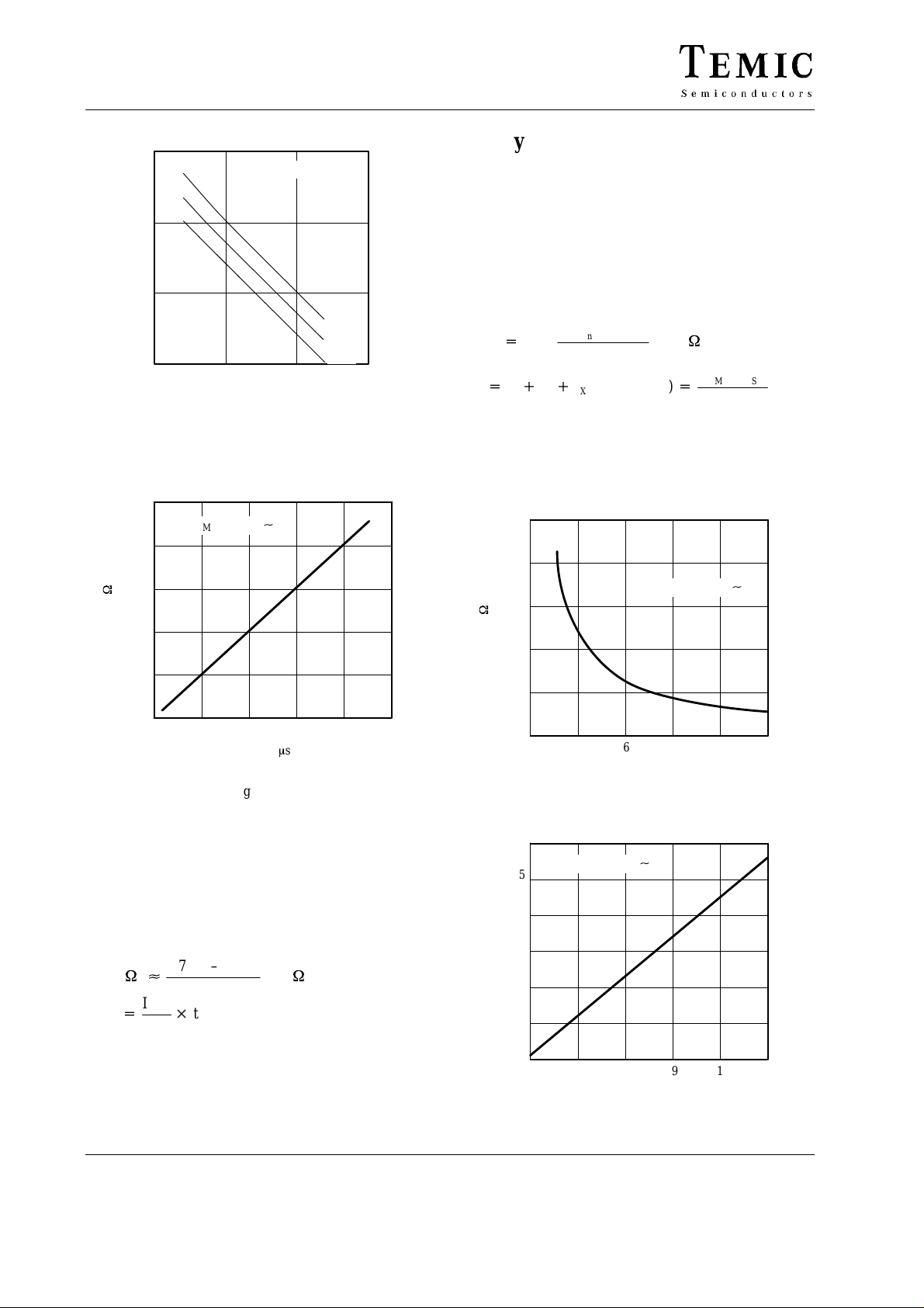
It depends on the latching current as well as on the load
current of the used triacs.
IL
[s]
t
p
whereas I
3
+
arcsin
4pf
[A] = Latching current of the triac
L
V
[V]= Mains voltage, effective
M
P[W] = Power load
f[1/s] = Mains frequency
Firing pulse width is specified through the zero cross over
identification which can be influenced by the sync.
resistance.
V
2Ǹsin
R
[W]
sync
+
M
where
[s] = required ignition pulse width
t
p
V
Ǹ
P 2
2
ǒ
w
3
2.5 10
M
Ǔ
t
–0.6
p
–5
–1.4 10
3
T
2
Figure 5. Protective circuit of the comparator
TELEFUNKEN Semiconductors
Rev . A1, 24-May-96
+
–
95 11412
3 (8)
Page 4
TEA1024/ TEA1124
t
10.00
p
t ( ms )
W
2
R ( M )
95 11
V
= 230 V∼
mains
1.00
I
( mA)
0.10
0.01
10 100 1000 10000
P ( W )96 11939
L
200
100
Figure 6.
2.5
V
=230V
Mains
2
1.5
1
0.5
0
0 200 400 600 800
X
tp ( ms )
Figure 7.
Supply Voltage
Due to higher trigger sensitivity of the triac it is supplied
with negative signal. It can be supplied via diode and
series resistance from the negative half wave of the mains.
An internal parallel controller limits the voltage between
Pin 5 and 7 to a typical value of 6.55 V.
Dimensioning of the Series Resistance
R
(Figures 8, 9)
1
V
–V
R
+
50
1max
+
IS)
I
tot
0.85
IP)
Mmin
I
X
VM= Mains supply
V
= Limiting voltage of the IC
S
I
= T otal current requirement
tot
I
= Current requirement for external circui
x
50
40
30
W
1
R ( k )
20
10
1000
0
03 6 912
95 10114
2I
tot
Figure 8.
Smax
I
tot
–65
P(R1)
( mA )
V
+
Mains
W
(V
=230V
–VS)
M
2R
X
2
1
15
Ignition (Firing) Current
The necessary ignition current depends on the specified
triac. With the help of a resistance, it is possible to limit
its value:
[W]
R
Gmax
[A]
+
I
p
whereas V
4 (8)
5.7V–V
[
I
Gmax
T
[V]= Gate voltage of the triac
G
I
[A]= Max. gate current
G
I
[A]= Average gate current requirement
P
t
[s] = Ignition pulse width
P
T[s] = Duration (of mains frequency)
Gmax
–25
I
Gmax
t
p
W
R1
P ( W )
95 10116
6
V
=230V
5
4
3
2
1
0
03 6 912
Mains
X
I
( mA )
tot
Figure 9.
TELEFUNKEN Semiconductors
Rev . A1, 24-May-96
15
Page 5
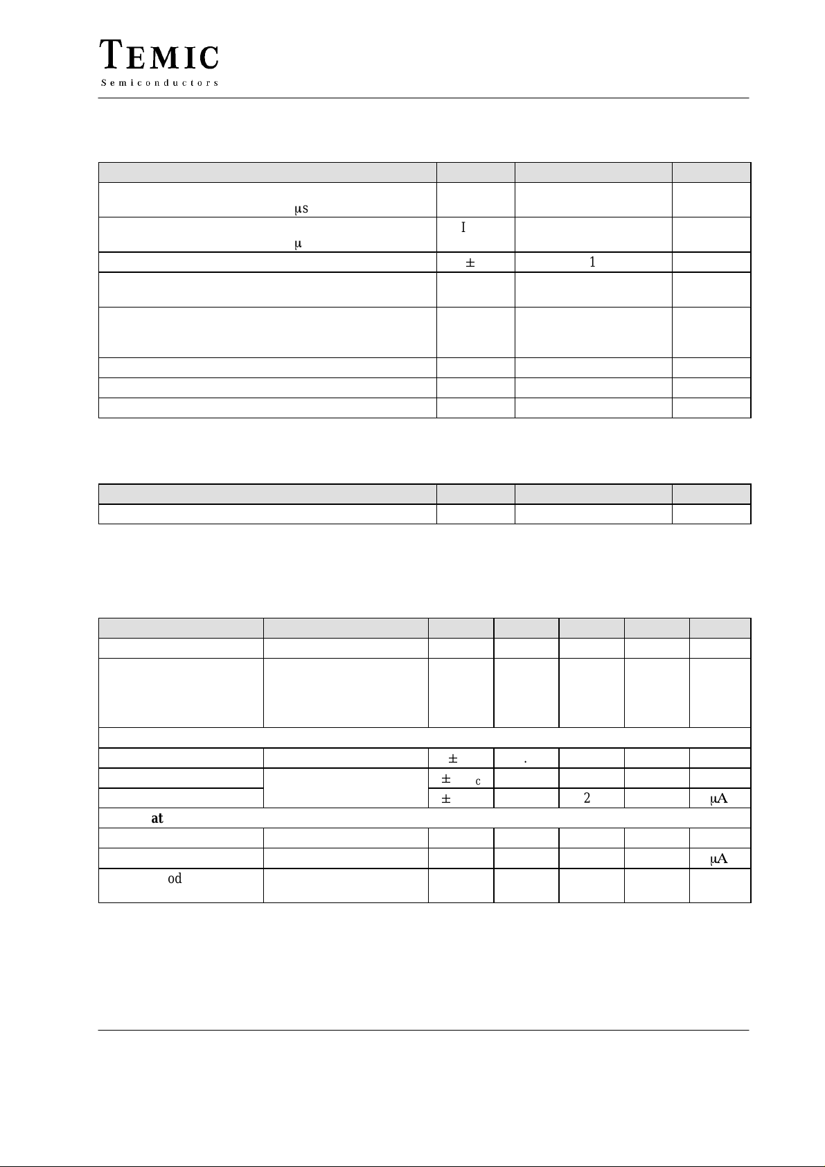
Absolute Maximum Ratings
Reference point Pin 6
Parameters Symbol Value Unit
Current consumption Pin 4
t ≤ 10 ms
Sync. current Pin 7
t ≤ 10 ms
Comparator input current Pin 2
Input voltages Pin 1,4,5
Pin 5
Power dissipation
T
= 45°C
amb
T
= 100°C
amb
Junction temperature T
Ambient temperature range T
Storage temperature range T
Thermal Resistance
TEA1024/ TEA1124
–I
I
Sync
i
Sync
"
–V
+V
P
i
s
tot
amb
stg
S
I
I
I
I
j
30
mA
150
5
mA
40
1 mA
≤ V
S
V
≤ 0.5
400
mW
125
125 °C
0 to 100 °C
–40 to + 125 °C
Parameters Symbol Maximum Unit
Junction ambient R
Electrical Characteristics
Supply voltage –V
Parameters Test Conditions / Pins Symbol Min Typ Max Unit
Supply voltage limitation –I
Current consumption Pos. half, cycle Pin 4
Synchronization Pin 7
Voltage limitation ±I
Synchronization current
Zero cross detection
Comparator, figure 5
Input zero voltage Pin 1, 2 V
Input quiescent current Pin 2 I
Common mode input
range
= 5.6 V, T
S
= 25°C, f = 50 Hz, reference point Pin 6, unless otherwise specified
amb
= 1 mA Pin 4 –V
4
Zero cross over
(Pin 5 open) Pin 4
neg. half cycle Pin 4
= 1 mA
7
"
"
"
Pin 1, 2 –V
–I
–I
–I
I
I
thJA
S
S
S
S
V
Sync
Sync
10
B
IC
200 K/W
5.7 7.4 V
1
mA
1
1.8
I
1.0 1.8 V
0.15 mA
25
mA
10 mV
1
mA
1 (VS–1.6) V
TELEFUNKEN Semiconductors
Rev . A1, 24-May-96
5 (8)
Page 6
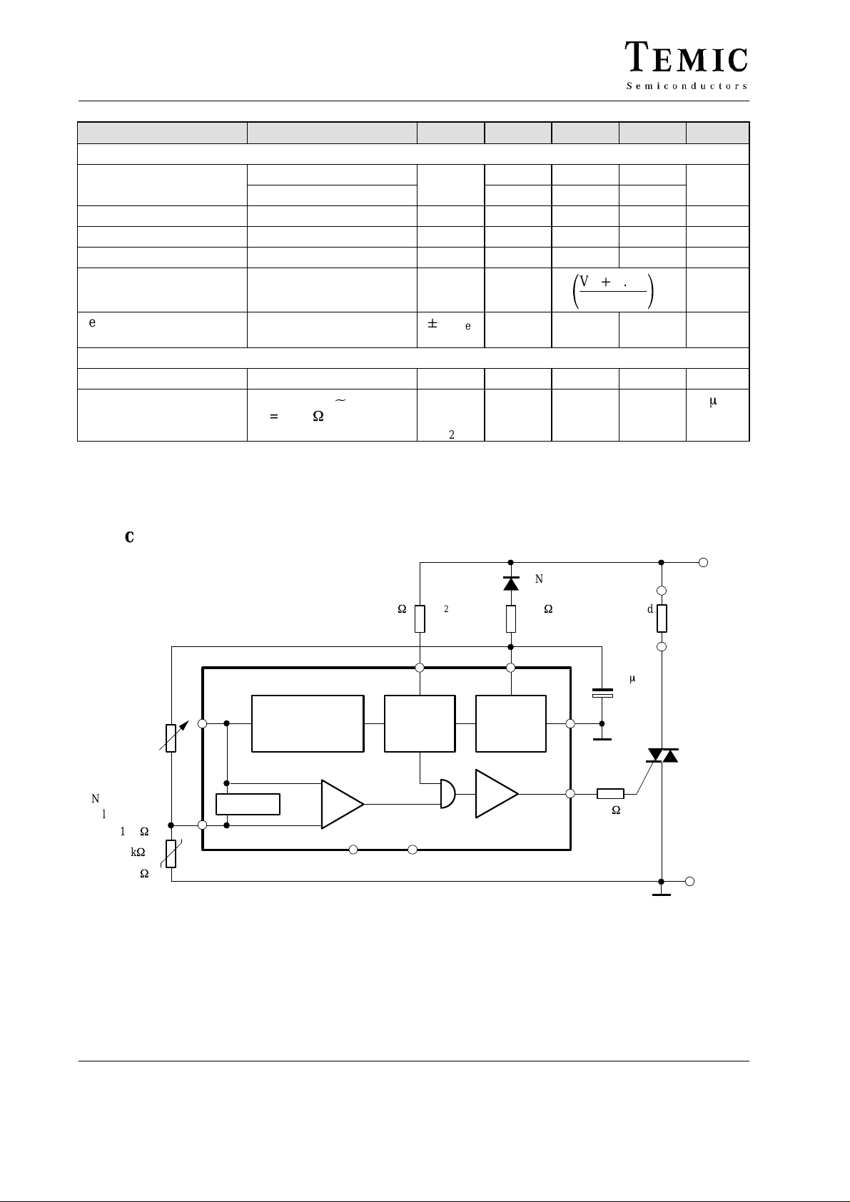
TEA1024/ TEA1124
Ramp generator, figures 3, 4 Pin 1
Period
TEA1024
T
TEA1124 1280
Step number n 16
Initial voltage –V
Final voltage –V
1
1
1.2 1.4 1.6 V
3.3 3.6 3.9 V
Internal reference
Temperature coefficient of
"
TC
Ref
internal reference
Pulse amplifier Pin 5
Output pulse current VG ≤1.5 V –I
Output pulse width V
R
Sync
2
= 220 k
= 230 VX,
W
O
t
0
t
1
t
2
50 100 mA
640
ǒ
110
UnitMaxTypMinSymbolTest Conditions / PinsParameters
ms
VS)
4–7.5%
2.5%
Ǔ
V
1.2 mV/K
33
m
s
65
Applications
95 11416
NTC / M87
B value = 3474
R
= 10 k
= 8 k
= 20 k
W
W
W
(25)
R
(30)
R
(10)
D
1N4007
1
R
2
(R
sync
7 4
8
R
)
22 kW/
1
2 W
Pulse
amplifier
C
1
6
5
1
Protection
2
Ramp generator
TEA 1024 – 640 ms
TEA 1124 –1280 ms
Comparator
+
–
NC NC
390 kW/
0.5 W
Sync. logic Supply
3
Figure 10. Simple temperature regulation with maximum proportional range
Load
0.7...1.5 kW
100 mF
16 V
TIC
236N
R
G
68
W
MT2
MT1
L
V
=
M
230 V ~
N
6 (8)
TELEFUNKEN Semiconductors
Rev . A1, 24-May-96
Page 7
TEA1024/ TEA1124
95 11417
R
10 k
R
2.2 k
6
12
33 k
50 k
NTC / M87
B value = 3474
R
= 10 k
= 8 k
= 20 k
W
W
W
(25)
R
(30)
R
(10)
R
4
W
R
p
W
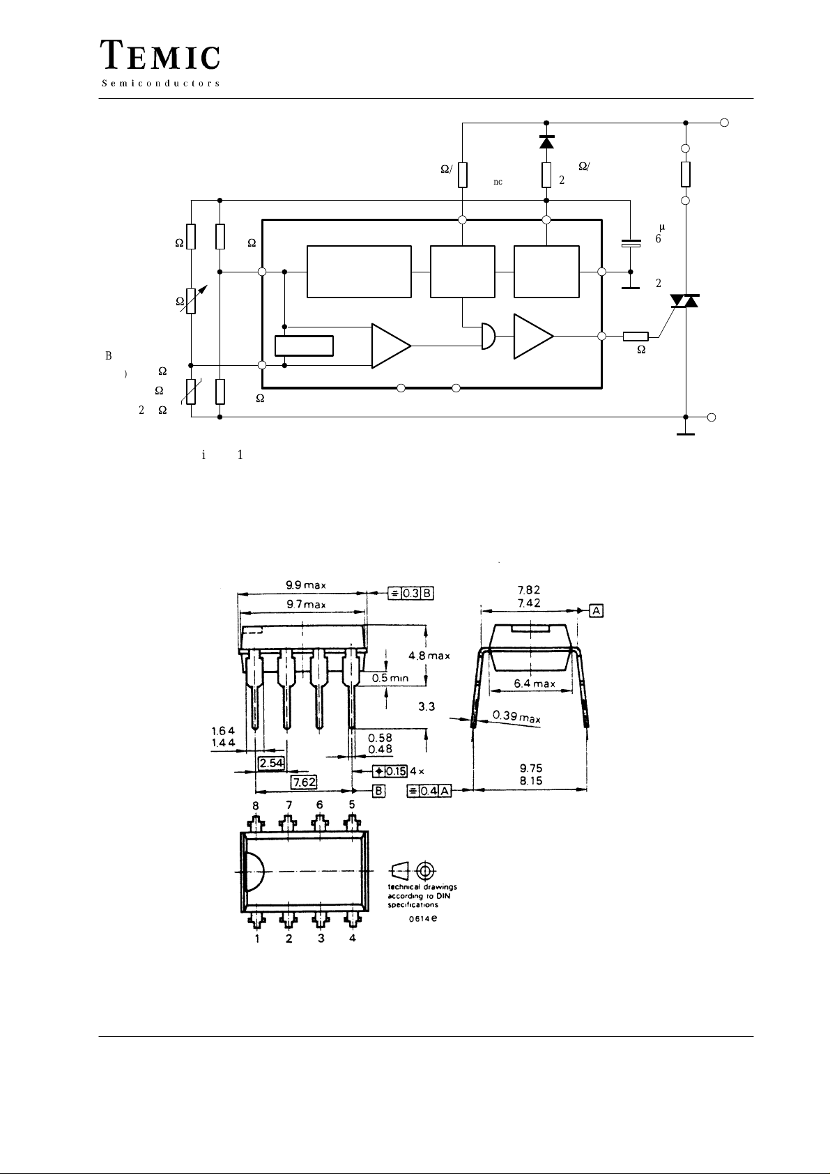
Figure 11. Temperature regulation with proportional range, 10 to 30 °C/ 640 ms ramp cycle
Dimensions in mm
W
W
1
Protection
2
Ramp generator
TEA1024 – 640 ms
TEA1124 –1280 ms
Comparator
+
–
NC NC
R
390 k
W/
0.5 W
Sync. logic Supply
3 8
2
(R
sync
7 4
V
230 V ~
MT2
MT1
L
=
M
N
D
1N4007
1
22 k
R
1
)
W/
2 W
C
6
5
Pulse
amplifier
Load
0.7...1.5 kW
100 mF
1
16 V
TIC
236N
R
G
68
W
Package: DIP8
TELEFUNKEN Semiconductors
Rev . A1, 24-May-96
7 (8)
Page 8

TEA1024/ TEA1124
Ozone Depleting Substances Policy Statement
It is the policy of TEMIC TELEFUNKEN microelectronic GmbH to
1. Meet all present and future national and international statutory requirements.
2. Regularly and continuously improve the performance of our products, processes, distribution and operating systems
with respect to their impact on the health and safety of our employees and the public, as well as their impact on
the environment.
It is particular concern to control or eliminate releases of those substances into the atmosphere which are known as
ozone depleting substances (ODSs).
The Montreal Protocol ( 1987) and its London Amendments (1990 ) intend to severely restrict the use of ODSs and
forbid their use within the next ten years. Various national and international initiatives are pressing for an earlier ban
on these substances.
TEMIC TELEFUNKEN microelectronic GmbH semiconductor division has been able to use its policy of
continuous improvements to eliminate the use of ODSs listed in the following documents.
1. Annex A, B and list of transitional substances of the Montreal Protocol and the London Amendments respectively
2. Class I and II ozone depleting substances in the Clean Air Act Amendments of 1990 by the Environmental
Protection Agency (EP A) in the USA
3. Council Decision 88/540/EEC and 91/690/EEC Annex A, B and C (transitional substances) respectively.
TEMIC can certify that our semiconductors are not manufactured with ozone depleting substances and do not contain
such substances.
We reserve the right to make changes to improve technical design and may do so without further notice.
Parameters can vary in different applications. All operating parameters must be validated for each customer
application by the customer. Should the buyer use TEMIC products for any unintended or unauthorized
application, the buyer shall indemnify TEMIC against all claims, costs, damages, and expenses, arising out of,
directly or indirectly, any claim of personal damage, injury or death associated with such unintended or
unauthorized use.
8 (8)
TEMIC TELEFUNKEN microelectronic GmbH, P.O.B. 3535, D-74025 Heilbronn, Germany
Telephone: 49 (0)7131 67 2831, Fax number: 49 (0)7131 67 2423
TELEFUNKEN Semiconductors
Rev . A1, 24-May-96
 Loading...