

Page 1

INTEGRATED CIRCUITS
DATA SH EET
TEA1507
GreenChipII SMPS control IC
Preliminary specification
File under Integrated Circuits, IC11
2000 Dec 05
Page 2
Philips Semiconductors Preliminary specification
GreenChipII SMPS control IC TEA1507
FEATURES
Distinctive features
• Universal mains supply operation (70 to 276 V AC)
• High level of integration, giving a very low external
component count.
Green features
• Valley/zero voltage switching for minimum switching
losses
• Efficient quasi-resonant operation at high power levels
• Frequency reductionat low power standby for improved
system efficiency (<3 W)
• Burst mode operation for very low standby levels(<1 W)
• On-chip start-up current source.
handbook, halfpage
1
2
TEA1507
3
4
8
7
6
5
Protection features
• Safe restart mode for system fault conditions
• Continuous mode protection by means of
demagnetization detection (zero switch-on current)
• Accurate and adjustable overvoltage protection
• Short winding protection
• Undervoltage protection (foldback during overload)
• Overtemperature protection
• Low and adjustable overcurrent protection trip level
• Soft (re)start
• Mains voltage-dependent operation-enabling level.
APPLICATIONS
Besides typical application areas, i.e. TV and Monitor
supplies, the device can be used in all applications that
demand an efficient and cost-effective solution up to
250 W.
MGU229
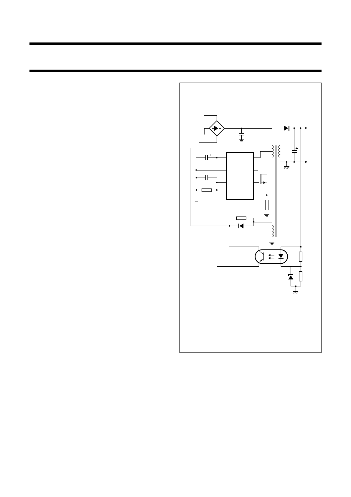
Fig.1 Typical application.
2000 Dec 05 2
Page 3

Philips Semiconductors Preliminary specification
GreenChipII SMPS control IC TEA1507
GENERAL DESCRIPTION
The GreenChipII is the second generation of green
Switched Mode Power Supply (SMPS) controller ICs
operatingdirectly from the rectified universalmains.A high
level of integration leads to a cost effective power supply
with a very low number of external components.
The special built-in green functions allow the efficiency to
be optimum at all power levels. This holds for
quasi-resonant operation at high power levels, as well as
fixed frequency operation with valley switching at medium
power levels. At low power (standby) levels, the system
operates at reduced frequency and with valley detection.
ORDERING INFORMATION
TYPE
NUMBER
TEA1507P DIP8 plastic dual in-line package; 8 leads (300 mil) SOT97-1
NAME DESCRIPTION VERSION
If burst modeoperation is applied,the standby powerlevel
can even be reduced to below 1 W.
The proprietary high voltage BCD800 process makes
direct start-up possible from the rectified mains voltage in
an effective and green way. A second low voltage
BICMOS IC is used for accurate, high speed protection
functions and control.
Highly efficient, reliable supplies can easily be designed
using the GreenChipII controller.
PACKAGE
2000 Dec 05 3
Page 4
This text is here in white to force landscape pages to be rotated correctly when browsing through the pdf in the Acrobat reader.This text is here in
a
_white to force landscape pages to be rotated correctly when browsing through the pdf in the Acrobat reader.This text is here inThis text is here in
white to force landscape pages to be rotated correctly when browsing through the pdf in the Acrobat reader. white to force landscape pages to be ...
2000 Dec 05 4
ndbook, full pagewidth
BLOCK DIAGRAM
Philips Semiconductors Preliminary specification
GreenChipII SMPS control IC TEA1507
V
CC
GND
CTRL
1
S1
2
3
2.5 V
M-level
−1
burst
detect
TEA1507
SUPPLY
MANAGEMENT
internal
FREQUENCY
UVLO start
supply
VOLTAGE
CONTROLLED
OSCILLATOR
CONTROL
OVER-
TEMPERATURE
PROTECTION
POWER-ON
RESET
MAXIMUM
ON-TIME
PROTECTION
UVLO
LOGIC
LOGIC
SQ
R
START-UP
CURRENT SOURCE
VALLEY
Q
100 mV
short
winding
OVER-
VOLTAGE
PROTECTION
DRIVER
LEB
blank
OCP
0.75 V
clamp
I
soft
start
S2
OVERPOWER
PROTECTION
8
DRAIN
HVS
7
n.c.
4
DEM
6
DRIVER
ss
0.5 V
5
I
sense
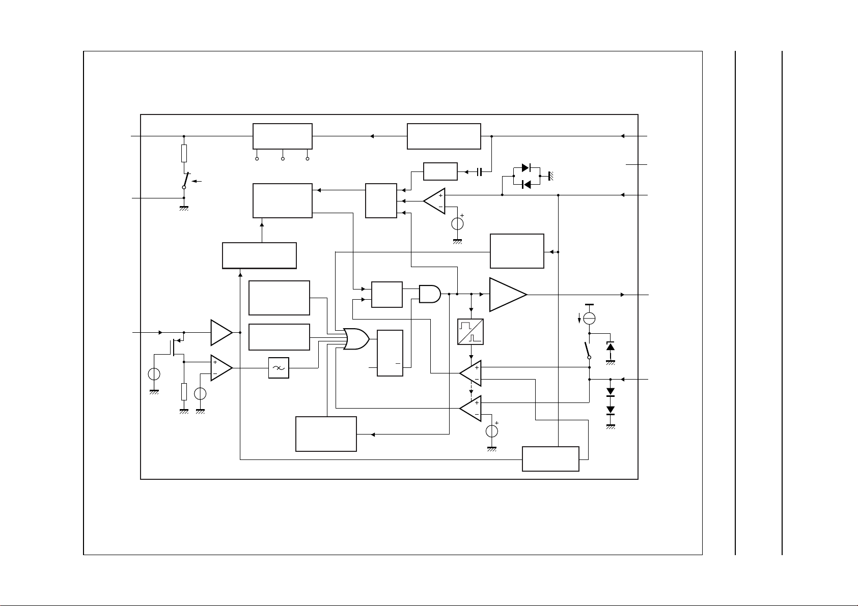
Fig.2 Block diagram.
MGU230
Page 5
Philips Semiconductors Preliminary specification
GreenChipII SMPS control IC TEA1507
PINNING
SYMBOL PIN DESCRIPTION
V
CC
GND 2 ground
CTRL 3 control input
DEM 4 input from auxiliary winding for
I
sense
DRIVER 6 gate driver output
HVS 7 high voltage safety spacer, not
DRAIN 8 drain of external MOS switch, input for
1 supply voltage
demagnetization timing, OVP and OPP
5 programmable current sense input
connected
start-up current and valley sensing
handbook, halfpage
1
V
CC
2
GND
CTRL
DEM
3
4
TEA1507
MGU231
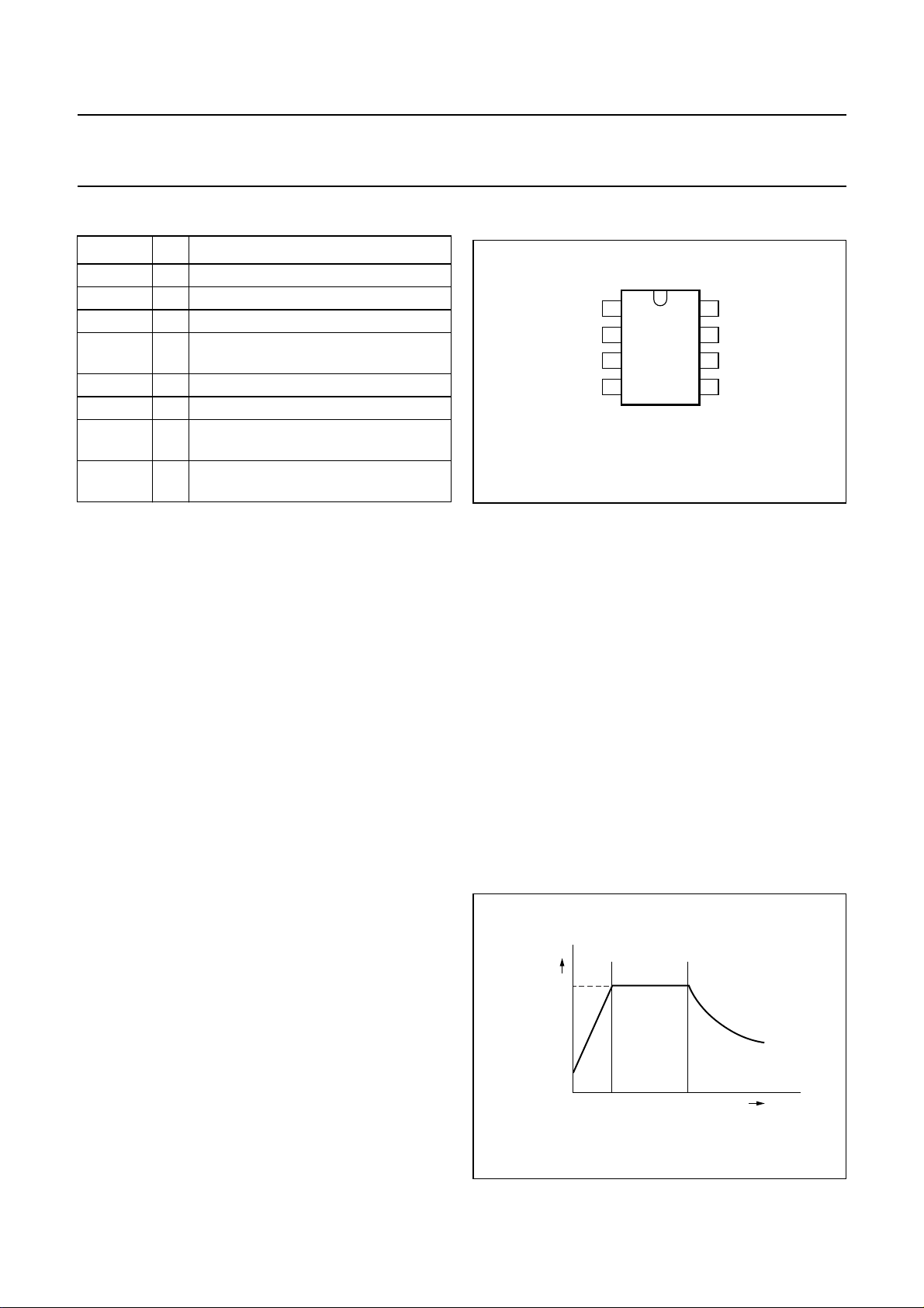
Fig.3 Pin configuration.
8
7
6
5
DRAIN
HVS
DRIVER
I
sense
FUNCTIONAL DESCRIPTION
The TEA1507 is the controller of a compact flyback
converter, with the IC situated at the primary side. An
auxiliary winding of the transformer provides
demagnetization detection and powers the IC after
start-up.
The TEA1507 operates in multi modes.
The next converter stroke is started only after
demagnetization of the transformer current (zero current
switching), while the drain voltage has reached the lowest
voltage to prevent switching losses (green function). The
primary resonant circuit of primary inductance and drain
capacitor ensures this quasi-resonant operation. The
design can be optimized in such a way that zero voltage
switching can be reached over almostthe universal mains
range.
To prevent very high frequency operation at lower loads,
the quasi-resonant operation changes smoothly in fixed
frequency PWM control.
At very low power (standby) levels, the frequency is
controlled down, via the VCO, to a minimum frequency of
about 6 kHz. Typically, 3 Watts can be achieved for a
75 W converter with an output power of 100 mW.
continue charging capacitor C
(switch S1 will be
VCC
opened), see Fig.2. The IC will activate the power
converter as soon as the voltage on pin VCC passes the
V
CC(start)
level. The IC supply is taken over by the auxiliary
windingas soon astheoutput voltage reachesitsintended
level and the IC supply from the mains voltage is
subsequently stopped for high efficiency operation (green
function).
The moment the voltage on pin VCC drops below the
V
(undervoltage lock out)level, the ICstops switching
UVLO
and enters a safe restart from the rectified mains voltage.
Inhibiting the auxiliary supply by external means causes
the converter to operate in a stable, well-defined burst
mode.
Supply management
All (internal) reference voltages are derived from a
temperature compensated, on-chip band gap circuit.
handbook, halfpage
175 kHz
f
VCO fixed quasi resonant
MGU232
Start-up, mains enabling operation level and
undervoltage lock out (see Figs. 10 and 11)
Initially, the IC is self supplying from the rectified mains
voltage via pin DRAIN. Supply capacitor C
is charged
VCC
by the internal start-up current source to a level of about
4 V or higher, depending on the drain voltage. Once the
drain voltage exceeds the M-level (mains-dependent
operation-enabling level), the start-up current source will
2000 Dec 05 5
6 kHz
power
Fig.4 Multi mode operation.
Page 6

Philips Semiconductors Preliminary specification
GreenChipII SMPS control IC TEA1507
Current mode control
Current mode control is used for its good line regulation
behaviour.
The ‘on-time’ iscontrolled by theinternally inverted control
pin voltage, which is compared with the primary current
information. The primary current is sensed across an
external resistor. The driver output is latched in the logic,
preventing multiple switch-on.
The internal control voltage is inverselyproportional to the
external control pin voltage, with an offset of 1.5 V. This
means that a voltage range from 1 to 1.5 V on pin CTRL
will result in an internal control voltage range from
0.5 to 0 V(the maximum externalcontrol voltage resultsin
a minimum duty cycle).
Oscillator
The maximum fixed frequency of the oscillator isset by an
internal current source and capacitor. The maximum
frequency is reduced once the control voltage enters the
VCO control window. Then, the maximum frequency
changeslinearly with thecontrol voltage untilthe minimum
frequency is reached (see Figs 5 and 6).
Valley switching (see Fig.7)
A new cycle starts when the power switch is switched on.
After the ‘on-time’ (which is determined by the ‘sense’
voltage and the internal control voltage), the switch is
opened and the secondary stroke starts. After the
secondary stroke, the drain voltage shows an oscillation
with a frequency of approximately
where L
is the primary self inductance of the transformer
p
---------------------------------------------------2 π× L
1
×()×()
pCd
and Cd is the capacitance on the drain node.
As soon as the oscillator voltage is high again and the
secondary stroke has ended, the circuit waits for the
lowest drain voltage before starting a new primary stroke.
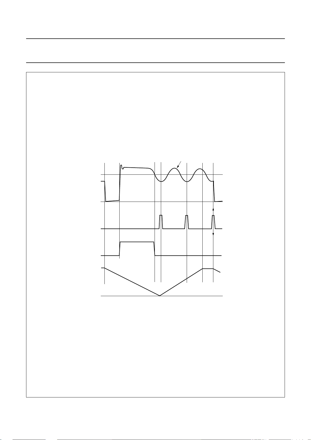
This method is called valley detection. Figure 7 shows the
drain voltage together with the valley signal, the signal
indicating the secondary stroke and the oscillator signal.
In an optimum design, the reflected secondary voltage on
the primary side will force the drain voltage to zero. Thus,
zero voltage switching is very possible, preventing large
1
capacitive switching losses , and
P
-- -
2
2
CV
× f××=
allowing high frequency operation, which results in small
and cost effective inductors.
Demagnetization
The system will be in discontinuous conduction mode all
the time. The oscillator will not start a new primary stroke
until the secondary stroke has ended.
Demagnetization features a cycle-by-cycle output
short-circuit protection by immediately lowering the
frequency (longer off-time), thereby reducing the power
level.
Demagnetizationrecognition is suppressedduringthe first
t
time. This suppression may be necessary in
suppr
applications where the transformer has a large leakage
inductance and at low output voltages/start-up.
Minimum and maximum ‘on-time’
The minimum ‘on-time’ of the SMPS is determined by the
Leading Edge Blanking (LEB) time. The IC limits the
‘on-time’ to 50 µs. When the system desires an ‘on-time’
longer than 50 µs, a fault condition is assumed (e.g.
removed Ci), the IC will stop switching and enter the safe
restart mode.
V
handbook, halfpage
sense(max)
Fig.5 The V
0.5 V
1 V
(typ)
sense(max)
1.5 V
(typ)
voltage as function of V
MGU233
V
CTRL
CTRL
.
2000 Dec 05 6
6 kHz
f
50 mV
(typ)
75 mV
V
(typ)
handbook, halfpage
Fig.6 The VCO frequency as function of V
MGU234
175 kHz
sense(max)
sense(max)
Page 7
Philips Semiconductors Preliminary specification
GreenChipII SMPS control IC TEA1507
handbook, full pagewidth
drain
valley
secondary
stroke
oscillator
primary
stroke
secondary
stroke
secondary
ringing
BA
MGU235
A: Start of new cycle at lowest drain voltage.
B: Start of new cycle in a classical PWM system at high drain voltage.
Fig.7 Signals for valley switching.
2000 Dec 05 7
Page 8

Philips Semiconductors Preliminary specification
GreenChipII SMPS control IC TEA1507
OverVoltage Protection (OVP)
An OVP mode is implemented in the GreenChip series.
For the TEA1507, this works by sensing the auxiliary
voltage via the current flowing into pin DEM during the
secondary stroke. The auxiliary winding voltage is a
well-defined replica of the output voltage. Any voltage
spikes are averaged by an internal filter.
If the output voltage exceeds the OVP trip level, the OVP
circuit switches the power MOSFET off. Next, the
controllerwaits until the UVLOlevel is reached onpin VCC.
This is followed by a safe restart cycle, after which
switching starts again.This process isrepeated as long as
the OVP condition exists.
Theoutput voltage atwhichthe OVP functiontrips,V
can be set by the demagnetization resistor, R
N
V
o OVP()
Where N
s
----------N
is the number of secondary turnsand N
s
I
(OVP)(DEM)RDEMVclamp DEM()pos()
aux
+×()×=
DEM
:
aux
o(OVP)
is the
number of auxiliary turns of the transformer.
Current I
The value of the demagnetization resistor (R
is internally trimmed.
ref
DEM
) can be
adjusted to the turns ratio of the transformer, thus making
an accurate OVP possible.
OverCurrent Protection (OCP)
MGU236
handbook, halfpage
−100 µA
(typ)
I
DEM
−24 µA
(typ)
V
sense(max)
0.50 V
(typ)
0.3 V
(typ)
Fig.8 OPP correction curve.
Short winding protection
After the leading edge blanking time, the short winding
protection circuit is also activated. If the ‘sense’ voltage
exceeds the short winding protection voltage V
swp
, the
converter will stop switching. Once VCC drops below the
UVLO level, capacitor C
will be recharged and the
VCC
supply will restart again. This cycle will be repeated until
the short circuit is removed (safe restart mode).
The short winding protection will also protect in case of a
secondary diode short circuit.
The cycle-by-cycle peak drain current limit circuit uses the
externalsource resistor to measurethecurrent accurately.
This allows optimum size determination of the transformer
core (cost issue). The circuit is activated after the leading
edge blanking time, t
. The OCP protection circuit limits
leb
the ‘sense’ voltage to an internal level.
OverPower Protection (OPP)
Duringthe primary stroke,the rectified mainsinput voltage
is measured by sensing the current drawn from pin DEM.
This current is dependent on the mains voltage, according
to the following formula:
N
aux
N
Where:
=
-----------N
p
V
I
DEM()
aux
≈≈
-------------- R
DEM
×
NV
mains
-------------------------R
DEM
The current information is used to adjust the peak drain
current, which is measured via pin I
. The internal
sense
compensation is such that an almost mains independent
maximum output power can be realized.
The OPP curve is given in Fig.8.
Overtemperature protection
An accurate temperature protection is provided in the
circuit. When the junction temperature exceeds the
thermal shutdown temperature, the IC will stop switching.
When VCC drops to UVLO, capacitor C
recharged to the V
level. If the temperature is still too
start
VCC
will be
high, VCC will drop again to the UVLO level, etc. (safe
restart mode).
Operation recommences when the junction temperature
drops 8 degrees typically.
2000 Dec 05 8
Page 9
Philips Semiconductors Preliminary specification
GreenChipII SMPS control IC TEA1507
Burst mode standby
Pin CTRL (pin 3)is also used to implementtheburst mode
standby. In burst mode standby, the power supply enters
aspecial low dissipation state,where it typically consumes
less than 1 W of input power (Po< 100 mW), but is still
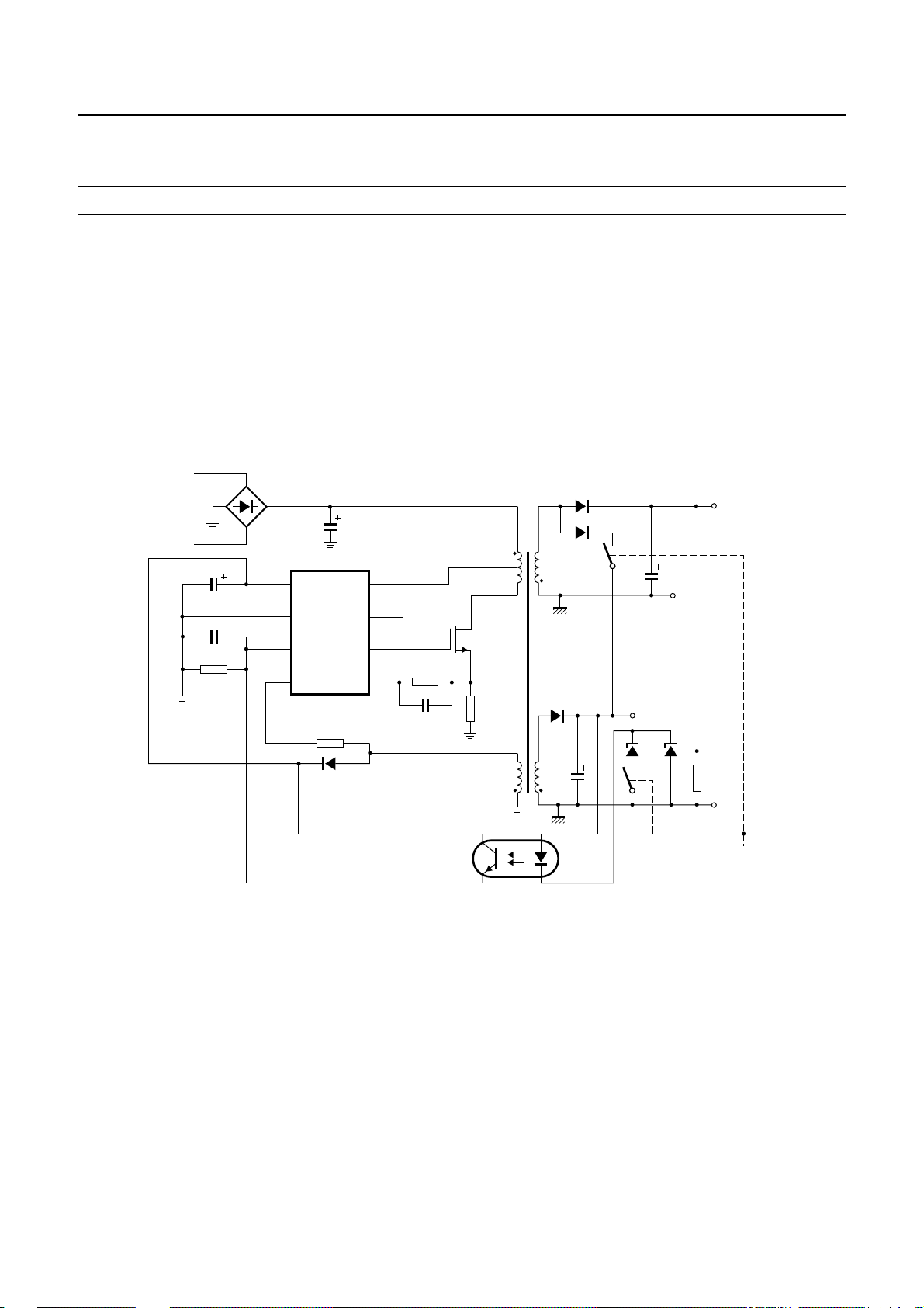
able to supply a microprocessor, for example. Figure 12
shows a flyback converter using the burst mode standby
function. The system enters burst mode standby when the
microprocessor closes switches S2 and S3 on the
secondary side. Switch S2 connects the high voltage
output secondary winding to the low voltage
microprocessor capacitor (CµC), bypassing Co.
When the voltage on CµC exceeds the Zener voltage, the
opto-coupler is activated, sending a largecurrent signal to
CTRL. In response to this signal, the IC stops switching
and enters a ‘hiccup’ mode. This burst activation signal
should be present for longer than the ‘burst blank’ period
(typically 30 µs): the blanking time prevents false burst
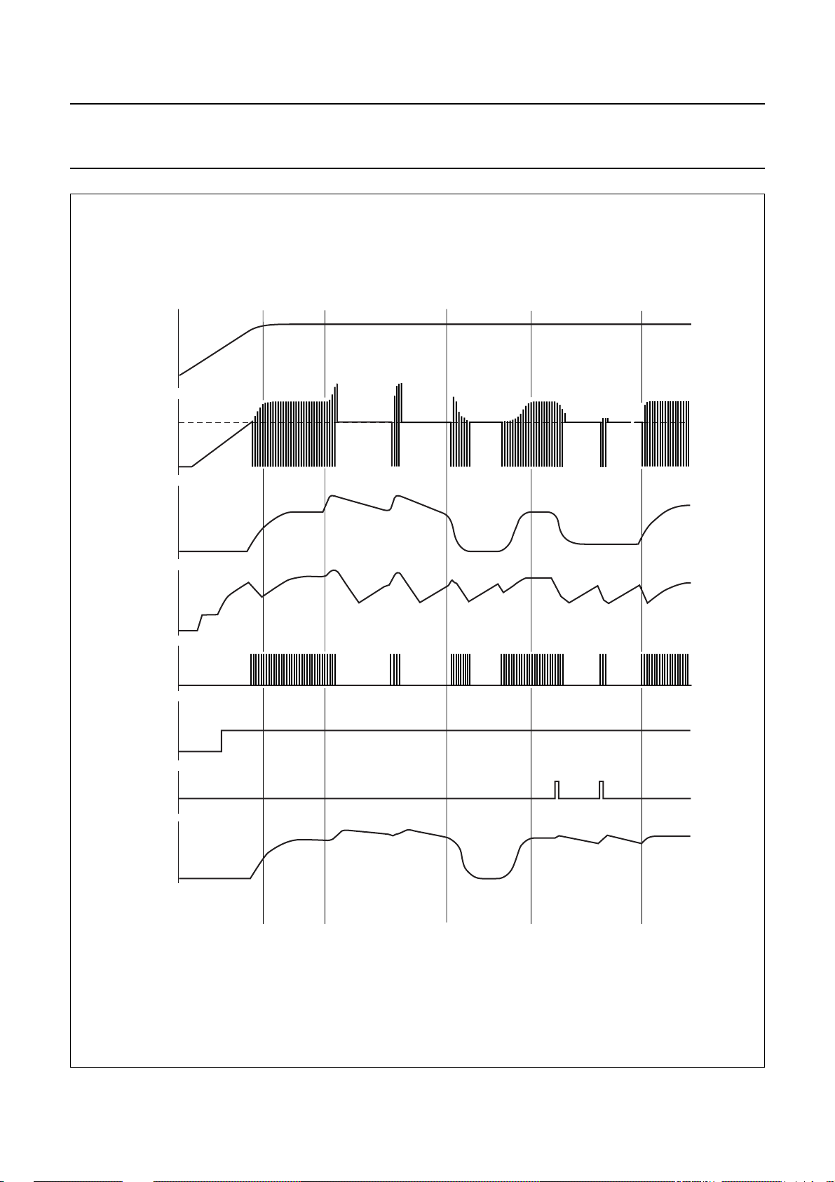
triggering due to spikes. Figure 11 shows the burst-mode
standby signals. The hiccup mode during burst mode
standby operation does not differ from the hiccup mode in
safe-restart mode during a system fault condition (e.g.
OVP or output short circuit). The power is reduced
during soft-restart mode.
Burst mode standby operation continues until the
microcontroller opens switches S2 and S3. The system
then enters the start-up sequence and begins normal
switching behaviour.
V
th
I
I
burstmode
---------------- R
CTRL
+=
th on()
(For burst mode specification, see Figs 11 and 12.)
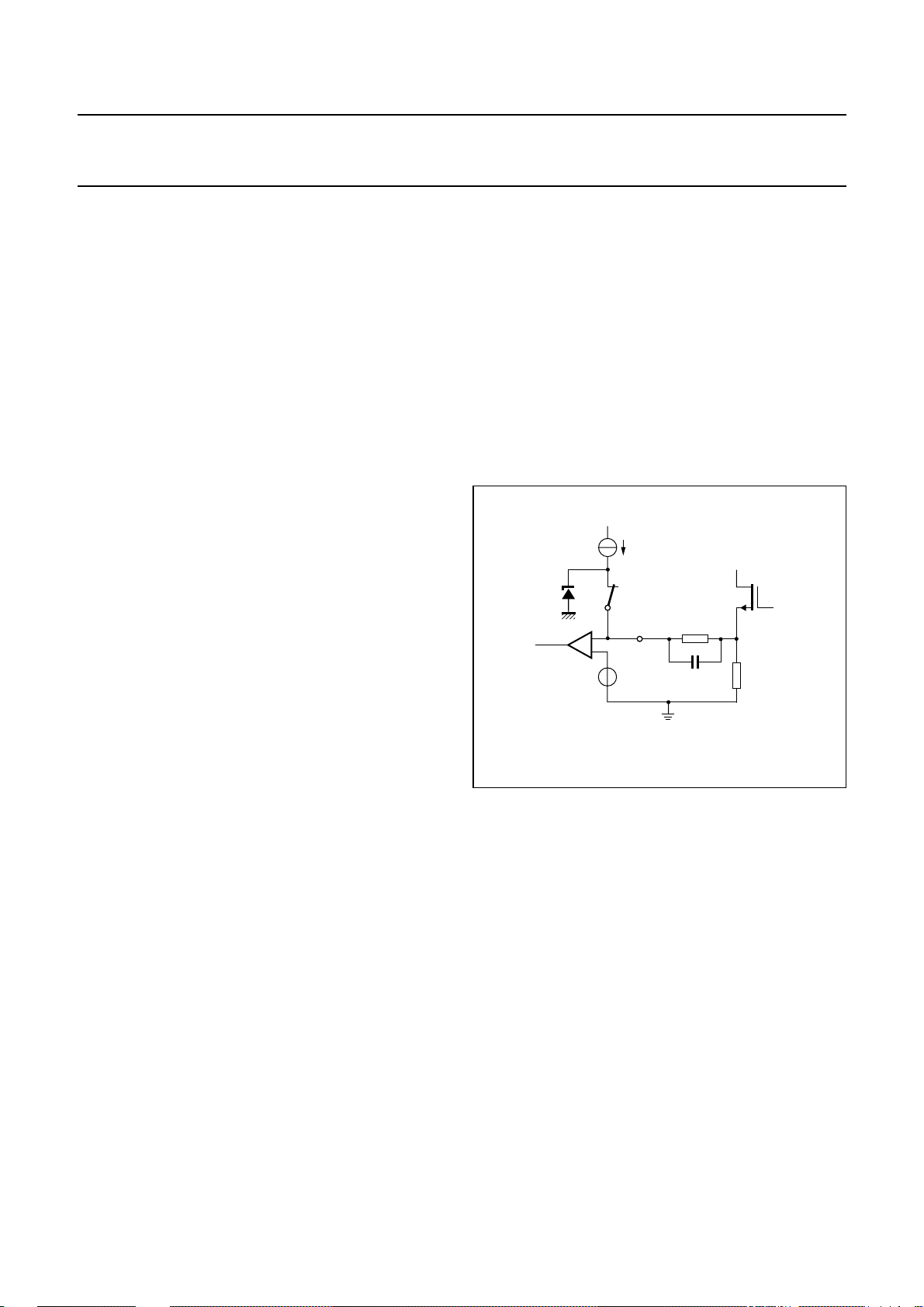
Soft start-up (pin I
sense
)
To prevent transformer rattle during hiccup, the
transformer peak current is slowly increased by the soft
start function. This can be achieved by inserting a resistor
and a capacitor between pin I
(pin 5) and the sense
sense
resistor. An internal current source charges the capacitor
to V = Iss× Rss, with a maximum of about 0.5 V.
The start level and the time constant of the increasing
primary current level can be adjusted externally by
changing the values of Rss and Css.
V
ocpIssRss
×=
ssCss
=
------------------------------------------- -
I
primary(max)
τ R
The charging current I
pin I
pin I
is below approximately 0.5 V. If the voltage on
sense
exceeds the 0.5 V, the soft start current source
sense
willstart limiting the currentIss.At the V
×()–
R
sense
will flow as long as the voltage on
ss
CC(start)
level,the I
current source is completely switched off (see Fig.9).
Since the soft start current Iss is subtracted from pin V
CC
charging current, theRssvalue will affectthe VCCcharging
current level by a maximum of 60 µA (typical value).
handbook, halfpage
0.5 V
I
SS
start-up
pin 5
I
sense
V
ocp
R
SS
C
SS
R
sense
MGU237
Fig.9 Soft start-up.
Driver
The driver circuit to the gate of the power MOSFET has a
current sourcing capability of typically 125 mA and a
current sink capability of typical 540 mA. This permits fast
turn-on and turn-off of the power MOSFET for efficient
operation.
A low driver source current has been chosen to limit the
∆V/∆t at switch-on. This reduces Electro Magnetic
Interference (EMI) and also limits the current spikes
across R
sense
.
ss
2000 Dec 05 9
Page 10
Philips Semiconductors Preliminary specification
GreenChipII SMPS control IC TEA1507
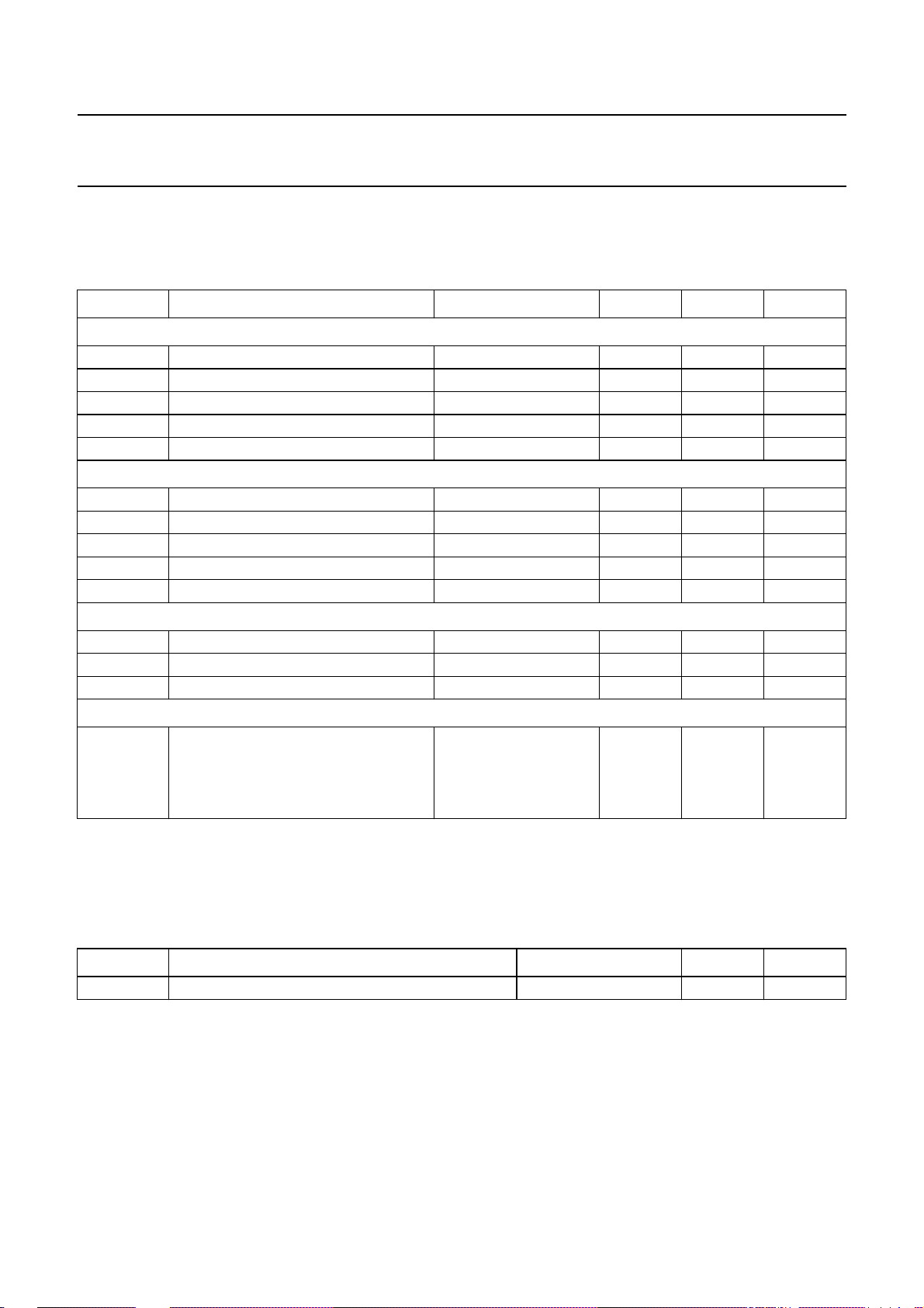
LIMITING VALUES
In accordance with the Absolute Maximum Rating System (IEC 60134). All voltages are measured with respect to
ground (pin 2); positive currents flow into the chip; pin 1 may not be current driven. The voltage ratings are valid
provided other ratings are not violated; current ratings are valid provided the maximum power rating is not violated.
SYMBOL PARAMETER CONDITIONS MIN. MAX. UNIT
Voltages
V
1
V
3
V
4
V
5
V
8
Currents
I
3
I
4
I
5
I
6
I
8
General
P
tot
T
stg
T
vj
ESD
V
ESD
pin 1 (VCC) continuous −0.4 +20 V
pin 3 (CTRL) −0.4 +5 V
pin 4 (DEM) current limited −0.4 − V
pin 5 (I
) current limited −0.4 − V
sense
pin 8 (DRAIN) −0.4 +650 V
pin 3 (CTRL) d < 10% − +50 mA
pin 4 (DEM) −250 +250 µA
pin 5 (I
) −1 +10 mA
sense
pin 6 (DRIVER) d < 10% −0.8 +2 A
pin 8 (DRAIN) − +5 mA
total power dissipation T
<55°C − 1.0 W
amb
storage temperature −55 +150 °C
virtual junction temperature −20 +145 °C
electrostatic discharge voltage class 1
human body model pins 1 to 6; note 1 − 1750 V
pin 8 (DRAIN); note 1 − 1000 V
machine model note 2 − 200 V
Notes
1. Equivalent to discharging a 100 pF capacitor through a 1.5 kΩ series resistor.
2. Equivalent to discharging a 200 pF capacitor through a 0.75 µH coil and a 10 Ω resistor.
THERMAL CHARACTERISTICS
SYMBOL PARAMETER CONDITIONS VALUE UNIT
R
th(j-a)
thermal resistance from junction to ambient in free air; note 1 100 K/W
Note
1. With pin GND connected to sufficient copper area on the printed-circuit board.
QUALITY SPECIFICATION
In accordance with ‘SNW-FQ-611-E’.
2000 Dec 05 10
Page 11
Philips Semiconductors Preliminary specification
GreenChipII SMPS control IC TEA1507
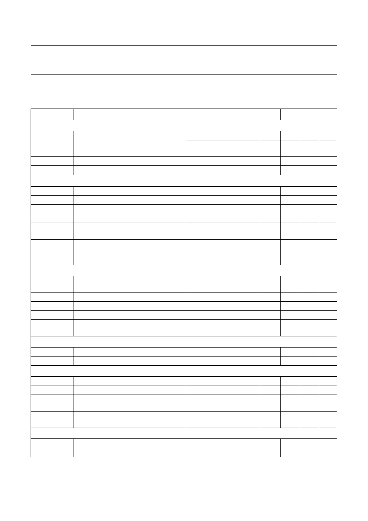
CHARACTERISTICS
T
=25°C; VCC= 15 V; all voltages are measured with respect to ground (pin 2); currents are positive when flowing
amb
into the IC; unless otherwise specified.
SYMBOL PARAMETER CONDITIONS MIN. TYP. MAX. UNIT
Start-up current source (pin 8)
I
i(DRAIN)
BV
DSS
M-level mains-dependent operation-enablinglevel 60 − 100 V
V
management (pin 1)
CC
V
CC(start)
V
CC(UVLO)
V
CC(hys)
I
i(VCC)H
I
i(VCC)L
I
VCC(restart)
I
CC(operate)
Demagnetization management (pin 4)
V
DEM
I
DEM
V
clamp(DEM)(neg)
V
clamp(DEM)(pos)
t
suppr
Pulse width modulator
t
on(min)
t
on(max)
Oscillator
f
oscL
f
oscH
V
vco(start)
V
vco(max)
Duty cycle control (pin 3)
V
CTRL(min)
V
CTRL(max)
supply current drawn from drain pin VCC=0V; V
with auxiliary supply;
V
DRAIN
> 100 V
> 100 V 1.0 1.2 1.4 mA
DRAIN
− 100 300 µA
breakdown voltage 650 −−V
start-up voltage on V
under voltage lock-out on V
hysteresis voltage on V
CC
CC
CC
pin VCC charging current V
pin VCC charging current V
pin VCC restart current V
V
CC(start)
DRAIN
DRAIN
− V
CC(UVLO)
> 100 V; VCC<3V −1.2 −1 −0.8 mA
> 100 V;
3V<VCC<V
> 100 V;
DRAIN
V
CC(UVLO)<VCC
CC(UVLO)
<V
CC(start)
10.3 11 11.7 V
8.1 8.7 9.3 V
2.0 2.3 2.6 V
−1.2 −0.75 −0.45 mA
−650 −550 −450 µA
supply current under normal operation no load on pin DRIVER 1.1 1.3 1.5 mA
demagnetization comparator threshold
50 100 150 mV
voltage on pin DEM
pin DEM current V
negative clamp voltage on pin DEM at I
positive clamp voltage on pin DEM at I
suppression of transformerringing atstart
=50mV −50
DEM
= −150 µA −0.5 −0.25 −0.05 V
DEM
= 250 µA 0.5 0.7 0.9 V
DEM
(1)
− 0nA
1.1 1.5 1.9 µs
of secondary stroke
minimum on-time − t
leb
− ns
maximum on-time latched 40 50 60 µs
oscillator low frequency (fixed frequency) V
oscillator high frequency (fixed frequency) V
peak voltage at pin I
sense
, where
> 1.5 V 5 6.5 8 kHz
CTRL
< 1 V 145 175 205 kHz
CTRL
see Fig.6 − 75 − mV
frequency reduction starts
peak voltage at pin I
frequency is equal to f
, where the
sense
oscL
− 50 − mV
min. voltage on CTRL (max. duty cycle) − 1.0 − V
max. voltage on CTRL (min. duty cycle) − 1.5 − V
2000 Dec 05 11
Page 12
Philips Semiconductors Preliminary specification
GreenChipII SMPS control IC TEA1507
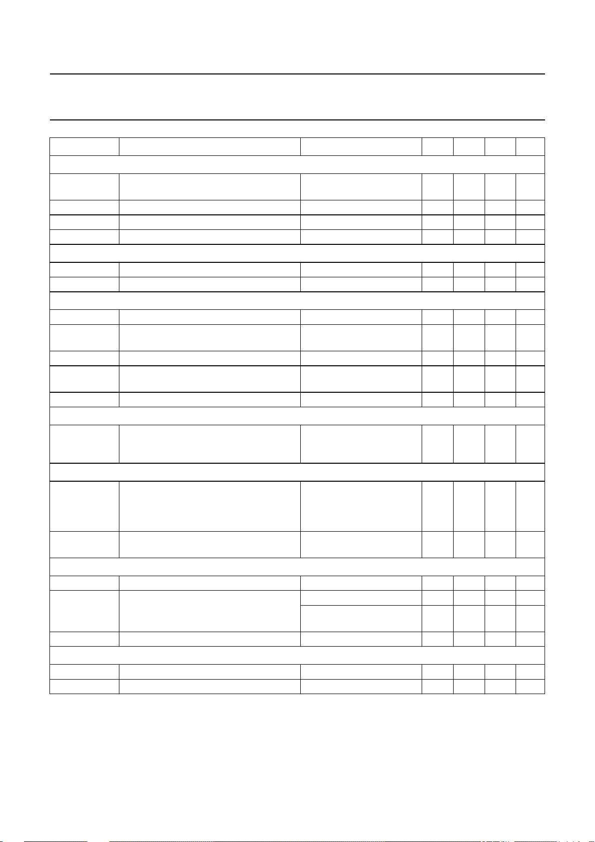
SYMBOL PARAMETER CONDITIONS MIN. TYP. MAX. UNIT
Burst mode standby (pin 3)
V
th(burst)(on)
burst mode standby active threshold
voltage
I
th(burst)(on)
I
th(burst)(off)
t
(burst-blank)
burst mode standby active current 16 −−mA
burst mode standby inactive current −−6mA
burst mode standby blanking time 25 30 35 µs
Valley switch (pin 8)
∆V/∆t
valley
t
valley-swon
∆V/∆t for valley recognition −85 −+85 V/µs
delay from valley recognition to switch-on − 150
Current and short winding protection (pin 5)
V
sense(max)
t
propagation
maximum source voltage OCP ∆V/∆t = 0.1 V/µs 0.48 0.52 0.56 V
delay from detecting V
sense(max)
switch-off
V
swp
t
leb
short winding protection voltage 0.83 0.88 0.96 V
blanking time for current and short
winding protection
I
ss
soft start current V
Overvoltage protection (pin 4)
I
(OVP)(DEM)
OVP protection level at pin 4, set by the
demagnetization resistor R
DEM
Section “OverVoltage Protection (OVP)”
Overpower protection (pin 4)
I
(OPP)(DEM)
OPP current at pin 4, start of OPP
correction. Set by the demagnetization
resistor R
; see Section “OverPower
DEM
Protection (OPP)”
I
(OPP50%)(DEM)
OPP current at pin 4 where maximum
source voltage is limited to 0.3 V
Driver (pin 6)
I
source
I
sink
V
o(driver)(max)
source current capability of driver VCC= 9.5 V; V
sink current capability of driver VCC= 9.5 V; V
maximum output voltage of the driver VCC>12V − 11.5 12 V
Temperature protection
T
prot(max)
T
prot(hyst)
maximum temperature threshold 130 140 150 °C
hysteresis temperature − 8
Note
1. Guaranteed by design.
to
; see
at I
= 6 mA 3.3 3.8 4.3 V
burst
(1)
− ns
∆V/∆t = 0.5 V/µs − 140 185 ns
300 370 440 ns
<0.5V 456075µA
sense
54 60 66 µA
−−24 −µA
−−100 −µA
=2V −−170 −88 mA
DRIVER
=2V − 300 − mA
DRIVER
V
CC
V
DRIVER
= 9.5 V;
= 9.5 V
400 700 − mA
(1)
−°C
2000 Dec 05 12
Page 13
Philips Semiconductors Preliminary specification
GreenChipII SMPS control IC TEA1507
APPLICATION INFORMATION
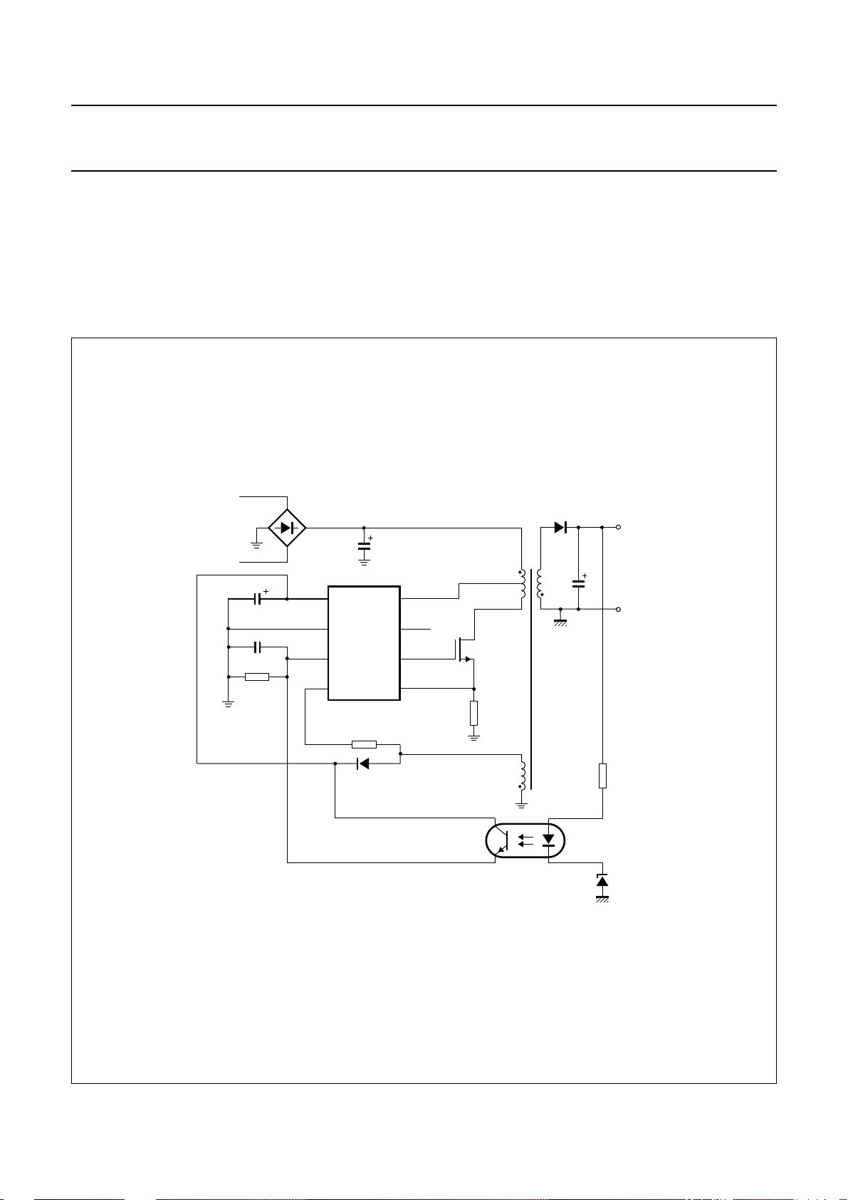
A converter with the TEA1507 consists of an input filter, a
transformer with a third winding (auxiliary), and an output
stage with a feedback circuit.
Capacitor C
(at pin 1) buffers the supply voltage of the
VCC
IC, which is powered via the high voltage rectified mains
V
handbook, full pagewidth
mains
C
C
R
VCC
CTRL
CTRL
V
CC
GND
CTRL
DEM
1
2
TEA1507
3
4
R
DEM
C
i
8
7
6
5
during start-up and via the auxiliary winding during
operation.
A sense resistor converts the primary current into a
voltageat pin I
(pin 5).The value of thissenseresistor
sense
defines the maximum primary peak current.
An application note is available: AN00047.
V
o
N
N
p
s
C
DRAIN
HVS
DRIVER
I
sense
n.c.
power
MOSFET
R
sense
o
Fig.10 Flyback configuration with secondary sensing.
2000 Dec 05 13
N
aux
MGU238
Page 14
Philips Semiconductors Preliminary specification
GreenChipII SMPS control IC TEA1507
handbook, full pagewidth
V
i
V
D
(power
MOSFET)
V
V
CC
V
gate
M-level
burst mode
V
i
o
V
µC
start-up
sequence
normal
operation
overvoltage
protection
Fig.11 Typical waveforms.
2000 Dec 05 14
output short
circuit
burst mode standby
normal
operation
MGU239
Page 15
Philips Semiconductors Preliminary specification
GreenChipII SMPS control IC TEA1507
handbook, full pagewidth
V
mains
C
C
R
VCC
CTRL
CTRL
V
CC
GND
CTRL
DEM
1
2
TEA1507
3
4
R
DEM
V
o
C
i
S2
8
7
6
5
DRAIN
HVS
DRIVER
I
sense
n.c.
power
MOSFET
R
SS
R
C
SS
sense
C
µC
C
o
microcontroller
supply
S3
burst mode
standby on/off
from microcontroller
MGU240
Fig.12 Flyback configuration with secondary sensing using the burst mode standby.
2000 Dec 05 15
Page 16
Philips Semiconductors Preliminary specification
GreenChipII SMPS control IC TEA1507
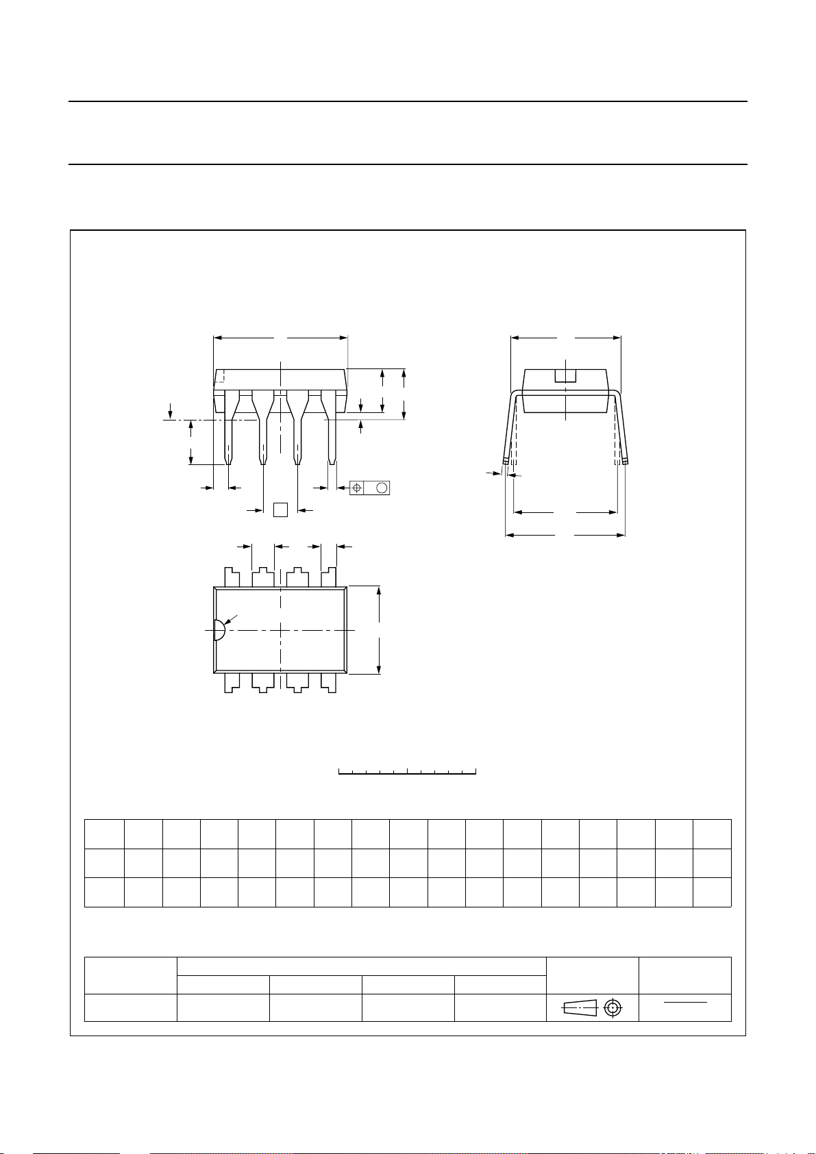
PACKAGE OUTLINE
DIP8: plastic dual in-line package; 8 leads (300 mil)
SOT97-1
seating plane
L
Z
8
pin 1 index
1
D
A
2
A
A
1
w M
b
e
b
1
b
2
5
E
4
M
E
c
(e )
1
M
H
0 5 10 mm
scale
DIMENSIONS (inch dimensions are derived from the original mm dimensions)
A
A
A
UNIT
max.
mm
inches
Note
1. Plastic or metal protrusions of 0.25 mm maximum per side are not included.
OUTLINE
VERSION
SOT97-1
12
min.
max.
1.73
1.14
0.068
0.045
IEC JEDEC EIAJ
050G01 MO-001 SC-504-8
b
b
0.53
0.38
0.021
0.015
1
1.07
0.89
0.042
0.035
b
2
REFERENCES
cD E e M
0.36
0.23
0.014
0.009
9.8
9.2
0.39
0.36
2000 Dec 05 16
(1) (1)
6.48
6.20
0.26
0.24
L
e
1
M
3.60
8.25
3.05
7.80
0.14
0.32
0.12
0.31
EUROPEAN
PROJECTION
E
10.0
0.39
0.33
H
8.3
w
max.
0.2542.54 7.62
ISSUE DATE
0.010.10 0.30
95-02-04
99-12-27
1.154.2 0.51 3.2
0.0450.17 0.020 0.13
(1)
Z
Page 17

Philips Semiconductors Preliminary specification
GreenChipII SMPS control IC TEA1507
SOLDERING
Introduction to soldering through-hole mount
packages
This text gives a brief insight to wave, dip and manual
soldering.A more in-depth accountofsoldering ICs can be
found in our
Packages”
Wave soldering is the preferred method for mounting of
through-hole mount IC packages on a printed-circuit
board.
Soldering by dipping or by solder wave
The maximum permissible temperature of the solder is
260 °C; solder at this temperature must not be in contact
with the joints for more than 5 seconds.
Suitability of through-hole mount IC packages for dipping and wave soldering methods
DBS, DIP, HDIP, SDIP, SIL suitable suitable
Note
1. For SDIP packages, the longitudinal axis must be parallel to the transport direction of the printed-circuit board.
“Data Handbook IC26; Integrated Circuit
(document order number 9398 652 90011).
PACKAGE
Thetotalcontact time of successive solderwavesmustnot
exceed 5 seconds.
The device may be mounted up to the seating plane, but
the temperature of the plastic body must not exceed the
specified maximum storage temperature (T
printed-circuit board has been pre-heated, forced cooling
may be necessary immediately after soldering to keep the
temperature within the permissible limit.
Manual soldering
Apply the soldering iron (24 V or less) to the lead(s) of the
package, either below the seating plane or not more than
2 mm above it. If the temperature of the soldering iron bit
is less than 300 °C it may remain in contact for up to
10 seconds. If the bit temperature is between
300 and 400 °C, contact may be up to 5 seconds.
SOLDERING METHOD
DIPPING WAVE
(1)
stg(max)
). If the
2000 Dec 05 17
Page 18

Philips Semiconductors Preliminary specification
GreenChipII SMPS control IC TEA1507
DATA SHEET STATUS
DATA SHEET STATUS
Objective specification Development This data sheet contains the design target or goal specifications for
Preliminary specification Qualification This data sheet contains preliminarydata, and supplementary data will be
Product specification Production This data sheet contains final specifications. Philips Semiconductors
Note
1. Please consult the most recently issued data sheet before initiating or completing a design.
DEFINITIONS
Short-form specification The data in a short-form
specification is extracted from a full data sheet with the
same type number and title. For detailed information see
the relevant data sheet or data handbook.
Limiting values definition Limiting values given are in
accordance with the Absolute Maximum Rating System
(IEC 60134). Stress above one or more of the limiting
values may cause permanent damage to the device.
These are stress ratings only and operation of the device
atthese or at anyother conditionsabovethose given in the
Characteristics sections of the specification is not implied.
Exposure to limiting values for extended periods may
affect device reliability.
Application information Applications that are
described herein for any of these products are for
illustrative purposes only. Philips Semiconductors make
norepresentationorwarranty that such applications willbe
suitable for the specified use without further testing or
modification.
PRODUCT
STATUS
DEFINITIONS
product development. Specification may change in any manner without
notice.
published at a later date. Philips Semiconductors reserves the right to
make changes at any time without notice in order to improve design and
supply the best possible product.
reserves the right to make changes at any time without notice in order to
improve design and supply the best possible product.
DISCLAIMERS
Life support applications These products are not
designed for use in life support appliances, devices, or
systems where malfunction of these products can
reasonably be expected to result inpersonal injury. Philips
Semiconductorscustomersusingor selling these products
for use in such applications do so at their own risk and
agree to fully indemnify Philips Semiconductors for any
damages resulting from such application.
Right to make changes Philips Semiconductors
reserves the right to make changes, without notice, in the
products, including circuits, standard cells, and/or
software, described or contained herein in order to
improve design and/or performance. Philips
Semiconductors assumes no responsibility or liability for
theuseof any of these products,conveysnolicence or title
under any patent, copyright, or mask work right to these
products,and makes no representationsorwarranties that
these products are free from patent, copyright, or mask
work right infringement, unless otherwise specified.
(1)
2000 Dec 05 18
Page 19

Philips Semiconductors Preliminary specification
GreenChipII SMPS control IC TEA1507
NOTES
2000 Dec 05 19
Page 20

Philips Semiconductors – a w orldwide compan y
Argentina: see South America
Australia: 3 Figtree Drive, HOMEBUSH, NSW 2140,
Tel. +61 2 9704 8141, Fax. +61 2 9704 8139
Austria: Computerstr. 6, A-1101 WIEN, P.O. Box 213,
Tel. +43 1 60 101 1248, Fax. +43 1 60 101 1210
Belarus: Hotel Minsk Business Center, Bld. 3, r. 1211, Volodarski Str. 6,
220050 MINSK, Tel. +375 172 20 0733, Fax. +375 172 20 0773
Belgium: see The Netherlands
Brazil: see South America
Bulgaria: Philips Bulgaria Ltd., Energoproject, 15th floor,
51 James Bourchier Blvd., 1407 SOFIA,
Tel. +359 2 68 9211, Fax. +359 2 68 9102
Canada: PHILIPS SEMICONDUCTORS/COMPONENTS,
Tel. +1 800 234 7381, Fax. +1 800 943 0087
China/Hong Kong: 501 Hong Kong Industrial Technology Centre,
72 Tat Chee Avenue, Kowloon Tong, HONG KONG,
Tel. +852 2319 7888, Fax. +852 2319 7700
Colombia: see South America
Czech Republic: see Austria
Denmark: Sydhavnsgade 23, 1780 COPENHAGEN V,
Tel. +45 33 29 3333, Fax. +45 33 29 3905
Finland: Sinikalliontie 3, FIN-02630 ESPOO,
Tel. +358 9 615 800, Fax. +358 9 6158 0920
France: 51 Rue Carnot, BP317, 92156 SURESNES Cedex,
Tel. +33 1 4099 6161, Fax. +33 1 4099 6427
Germany: Hammerbrookstraße 69, D-20097 HAMBURG,
Tel. +49 40 2353 60, Fax. +49 40 2353 6300
Hungary: see Austria
India: Philips INDIA Ltd, Band Box Building, 2nd floor,
254-D, Dr. Annie Besant Road, Worli, MUMBAI 400 025,
Tel. +91 22 493 8541, Fax. +91 22 493 0966
Indonesia: PT Philips DevelopmentCorporation, Semiconductors Division,
Gedung Philips, Jl. Buncit Raya Kav.99-100, JAKARTA 12510,
Tel. +62 21 794 0040 ext. 2501, Fax. +62 21 794 0080
Ireland: Newstead, Clonskeagh, DUBLIN 14,
Tel. +353 1 7640 000, Fax. +353 1 7640 200
Israel: RAPAC Electronics, 7 Kehilat Saloniki St, PO Box 18053,
TEL AVIV 61180, Tel. +972 3 645 0444, Fax. +972 3 649 1007
Italy: PHILIPS SEMICONDUCTORS, Via Casati, 23 - 20052 MONZA (MI),
Tel. +39 039 203 6838, Fax +39 039 203 6800
Japan: Philips Bldg 13-37, Kohnan 2-chome, Minato-ku,
TOKYO 108-8507, Tel. +81 3 3740 5130, Fax. +81 3 3740 5057
Korea: Philips House, 260-199 Itaewon-dong, Yongsan-ku, SEOUL,
Tel. +82 2 709 1412, Fax. +82 2 709 1415
Malaysia: No. 76 Jalan Universiti, 46200 PETALING JAYA, SELANGOR,
Tel. +60 3 750 5214, Fax. +60 3 757 4880
Mexico: 5900 Gateway East, Suite 200, EL PASO, TEXAS 79905,
Tel. +9-5 800 234 7381, Fax +9-5 800 943 0087
Middle East: see Italy
Netherlands: Postbus 90050, 5600 PB EINDHOVEN, Bldg. VB,
Tel. +31 40 27 82785, Fax. +31 40 27 88399
New Zealand: 2 Wagener Place, C.P.O. Box 1041, AUCKLAND,
Tel. +64 9 849 4160, Fax. +64 9 849 7811
Norway: Box 1, Manglerud 0612, OSLO,
Tel. +47 22 74 8000, Fax. +47 22 74 8341
Pakistan: see Singapore
Philippines: Philips Semiconductors Philippines Inc.,
106 Valero St. Salcedo Village, P.O. Box 2108 MCC, MAKATI,
Metro MANILA, Tel. +63 2 816 6380, Fax. +63 2 817 3474
Poland: Al.Jerozolimskie 195 B, 02-222 WARSAW,
Tel. +48 22 5710 000, Fax. +48 22 5710 001
Portugal: see Spain
Romania: see Italy
Russia: Philips Russia, Ul. Usatcheva 35A, 119048 MOSCOW,
Tel. +7 095 755 6918, Fax. +7 095 755 6919
Singapore: Lorong 1, Toa Payoh, SINGAPORE 319762,
Tel. +65 350 2538, Fax. +65 251 6500
Slovakia: see Austria
Slovenia: see Italy
South Africa: S.A. PHILIPS Pty Ltd., 195-215 Main Road Martindale,
2092 JOHANNESBURG, P.O. Box 58088 Newville 2114,
Tel. +27 11 471 5401, Fax. +27 11 471 5398
South America: Al. Vicente Pinzon, 173, 6th floor,
04547-130 SÃO PAULO, SP, Brazil,
Tel. +55 11 821 2333, Fax. +55 11 821 2382
Spain: Balmes 22, 08007 BARCELONA,
Tel. +34 93 301 6312, Fax. +34 93 301 4107
Sweden: Kottbygatan 7, Akalla, S-16485 STOCKHOLM,
Tel. +46 8 5985 2000, Fax. +46 8 5985 2745
Switzerland: Allmendstrasse 140, CH-8027 ZÜRICH,
Tel. +41 1 488 2741 Fax. +41 1 488 3263
Taiwan: Philips Semiconductors, 5F, No. 96, Chien Kuo N. Rd., Sec. 1,
TAIPEI, Taiwan Tel. +886 2 2134 2451, Fax. +886 2 2134 2874
Thailand: PHILIPS ELECTRONICS (THAILAND) Ltd.,
60/14 MOO 11, Bangna Trad Road KM. 3, Bagna, BANGKOK 10260,
Tel. +66 2 361 7910, Fax. +66 2 398 3447
Turkey: Yukari Dudullu, Org. San. Blg., 2.Cad. Nr. 28 81260 Umraniye,
ISTANBUL, Tel. +90 216 522 1500, Fax. +90 216 522 1813
Ukraine: PHILIPS UKRAINE, 4 Patrice Lumumba str., Building B, Floor 7,
252042 KIEV, Tel. +380 44 264 2776, Fax. +380 44 268 0461
United Kingdom: Philips Semiconductors Ltd., 276 Bath Road, Hayes,
MIDDLESEX UB3 5BX, Tel. +44 208 730 5000, Fax. +44 208 754 8421
United States: 811 East Arques Avenue, SUNNYVALE, CA 94088-3409,
Tel. +1 800 234 7381, Fax. +1 800 943 0087
Uruguay: see South America
Vietnam: see Singapore
Yugoslavia: PHILIPS, Trg N. Pasica 5/v, 11000 BEOGRAD,
Tel. +381 11 3341 299, Fax.+381 11 3342 553
For all other countries apply to: Philips Semiconductors,
Marketing Communications, Building BE-p, P.O. Box 218, 5600 MD EINDHOVEN,
The Netherlands, Fax. +31 40 27 24825
© Philips Electronics N.V. SCA
All rights are reserved. Reproduction in whole or in part is prohibited without the prior written consent of the copyright owner.
The information presented in this document does not form part of any quotation or contract, is believed to be accurate and reliable and may be changed
without notice. No liability will be accepted by the publisher for any consequence of its use. Publication thereof does not convey nor imply any license
under patent- or other industrial or intellectual property rights.
2000
Internet: http://www.semiconductors.philips.com
70
Printed in The Netherlands 613502/01/pp20 Date of release: 2000 Dec 05 Document order number: 9397 750 07298
 Loading...