


INTEGRATED CIRCUITS
NE56605-42
System reset with built-in watchdog timer
Product data
Supersedes data of 2001 Apr 24
File under Integrated Circuits, Standard Analog
2001 Aug 22
Philips Semiconductors Product data
TYPE NUMBER
NE56605-42System reset with built-in watchdog timer
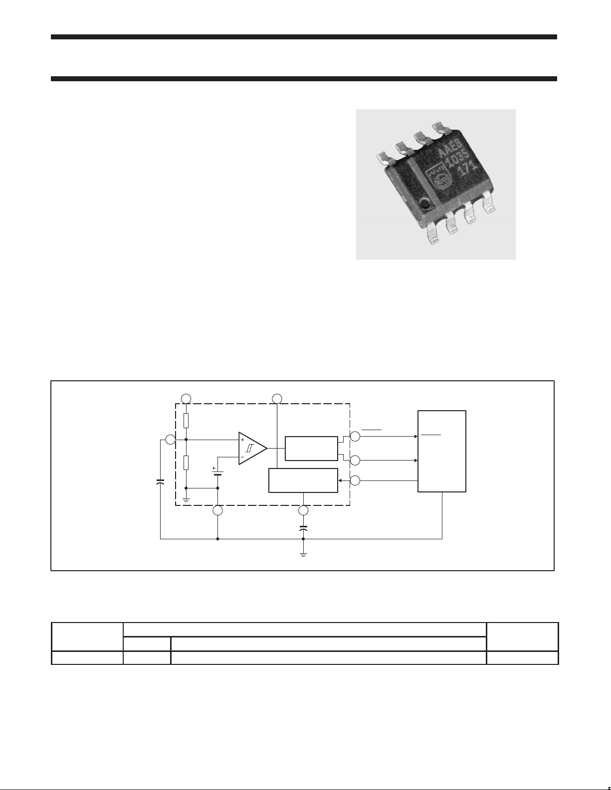
GENERAL DESCRIPTION
The NE56605-42 is designed to generate a reset signal, at a
threshold voltage of 4.2 V , for a variety of microprocessor and logic
systems. Accurate reset signals are generated during momentary
power interruptions, or whenever power supply voltages sag to
intolerable levels. The NE56605-42 has a built-in Watchdog Timer to
monitor the microprocessor and ensure it is operating properly. Any
abnormal system operations due to microprocessor malfunctions
are terminated by the watchdog’s generating a system reset. The
NE56605-42 has a watchdog monitoring time of 10 ms (typical).
The NE56605-42 is offered in the SO8 surface mount package.
FEATURES
•Both positive and negative logic reset output signals are available
•Accurate threshold detection
•Internal power-on reset delay
•Internal watchdog timer programmable with external capacitor
•Watchdog monitoring time of 10 ms
•Reset assertion with V
down to 0.8 VDC (typical)
CC
•Few external components required.
APPLICA TIONS
•Microcomputer systems
•Logic systems.
SIMPLIFIED SYSTEM DIAGRAM
V
CC
5
NE56605-42
V
S
C
R
7
V
R
REF
4
GND
WD
6
C
RESET
GENERATOR
PROGRAMMABLE
WATCHDOG TIMER
1
C
T
8
2
3
RESET
RESET
CLK
LOGIC
SYSTEM
RESET
RESET
CLK
GND
SL01282
Figure 1. Simplified system diagram.
ORDERING INFORMATION
PACKAGE
NAME DESCRIPTION
NE56605-42D SO8 plastic small outline package; 8 leads; body width 3.9 mm –20 to +70 °C
TEMPERATURE
RANGE
2001 Aug 22 853–2251 26949
2
Philips Semiconductors Product data
NE56605-42System reset with built-in watchdog timer
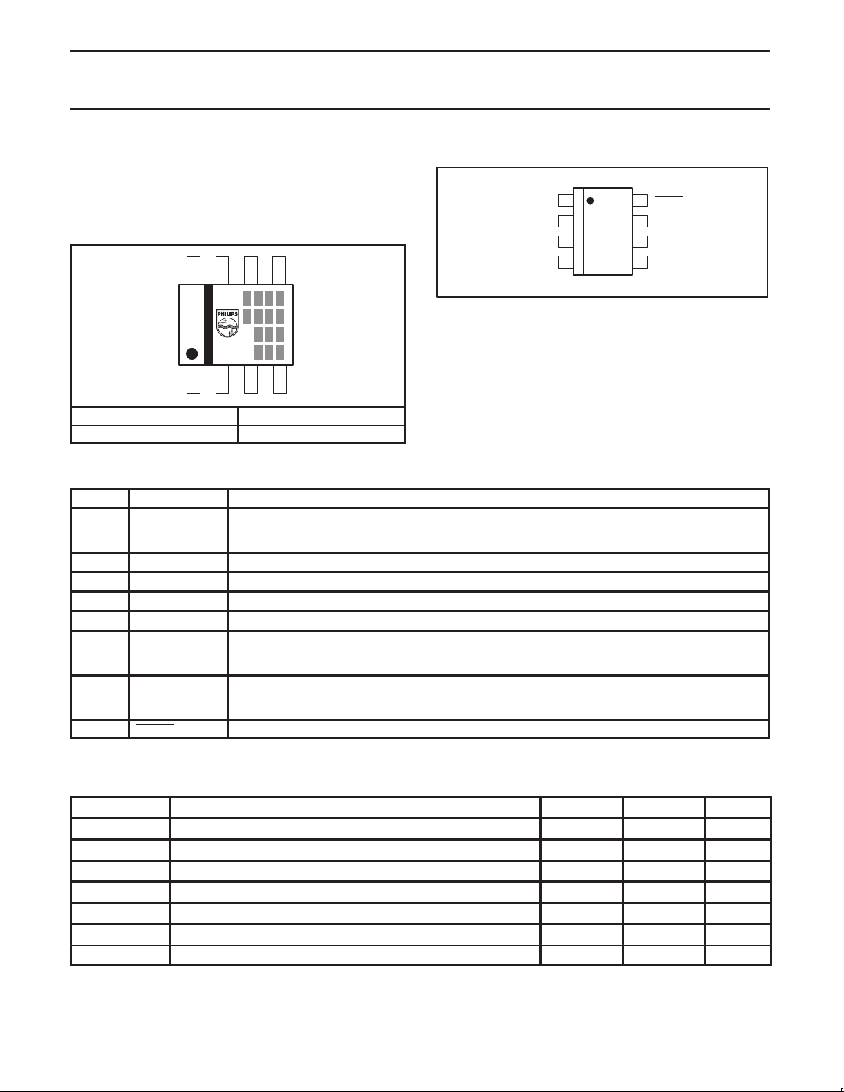
Part number marking
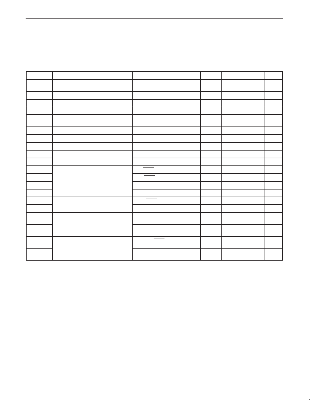
PIN CONFIGURATION
The package is marked with a four letter code in the first line to the
right of the logo. The first three letters designate the product. The
fourth letter, represented by ‘x’, is a date tracking code. The
remaining two or three lines of characters are internal manufacturing
codes.
5
6
7
8
2
1
3
4
Part number Marking
NE56605-42 A A E x
PIN DESCRIPTION
PIN SYMBOL DESCRIPTION
1 C
T
2 RESET Reset HIGH output pin.
3 CLK Clock input pin from logic system for watchdog timer.
4 GND Circuit ground.
5 V
6 WD
7 V
CC
C
S
8 RESET Reset LOW output pin.
t
, t
WDM
t
WDM
Diagram) for definition of t
, tPR adjustment pin.
WDR
, t
, tPR times are dependent on the value of external CT capacitor used. See Figure 18 (Timing
WDR
WDM
, t
WDR
, tPR times.
Power supply pin for circuit.
Watchdog timer control pin.
The watchdog timer is enabled when this pin is unconnected, and disabled when this pin is connected to
ground.
Detection threshold adjustment pin.
The detection threshold can be increased by connecting this pin to VCC with a pull-up resistor. The detection
threshold can be decreased by connecting this pin to ground with a pull-down resistor.
TOP VIEW
8
7
6
5
SL01279
RESET
CLK
GND
1
C
T
2
SO8
3
4
Figure 2. Pin configuration.
RESET
V
S
WD
C
V
CC
MAXIMUM RATINGS
SYMBOL PARAMETER MIN. MAX. UNIT
V
CC
V
S
V
CLK
V
OH
T
oper
T
stg
P Power dissipation – 250 mW
2001 Aug 22
Power supply voltage –0.3 10 V
VS pin voltage –0.3 10 V
CLK pin voltage –0.3 10 V
RESET and RESET pin voltage –0.3 10 V
Operating temperature –20 70 °C
Storage temperature –40 125 °C
3
Philips Semiconductors Product data
NE56605-42System reset with built-in watchdog timer
DC ELECTRICAL CHARACTERISTICS
Characteristics measured with VCC = 5.0 V, and T
See Figure 23 (Test circuit 1) for test configuration used for DC parameters.
SYMBOL PARAMETER CONDITIONS MIN. TYP. MAX. UNIT
I
CC
V
SL
V
SH
∆VS/∆T
V
hys
V
TH
I
IH
I
IL
V
OH1
V
OH2
V
OL1
V
OL2
V
OL3
V
OL4
I
OL1
I
OL2
I
CT1
I
CT2
V
CCL1
V
CCL2
Supply current during watchdog timer
operation
Reset detection threshold VS = open; VCC = falling 4.05 4.20 4.35 V
Reset detection threshold VS = open; VCC = rising 4.15 4.30 4.45 V
Temperature coefficient of reset threshold –20 °C ≤ T
amb
Reset threshold hysteresis V
CLK input threshold 0.8 1.2 2.0 V
CLK input current, HIGH-level V
CLK input current, LOW-level V
Output voltage, HIGH-level
Output voltage, LOW-level
Output sink current
CT charge current
Supply voltage to assert reset operation
= 25 °C, unless otherwise specified.
amb
amb
= VSH (rising VCC) – V
HYS
(falling VCC)
= 5.0 V – 0 1.0 µA
CLK
= 0 V –20 –10 –3.0 µA
CLK
I
= –5.0 µA; VS = open 4.5 4.8 – V
RESET
I
current = –5.0 mA; VS = 0 V 4.5 4.8 – V
RESET
I
= 3.0 mA; VS = 0 V – 0.2 0.4 V
RESET
I
= 10 mA; VS = 0 V – 0.3 0.5 V
RESET
I
= 0.5 mA; VS = open – 0.2 0.4 V
RESET
I
= 1.0 mA; VS = open – 0.3 0.5 V
RESET
V
= 1.0 V; VS = 0 V 10 16 – mA
RESET
V
= 1.0 V; VS = open 1.0 2.0 – mA
RESET
VCT = 1.0 V; WDC = open during
watchdog operation
VCT = 1.0 V;
during power-on reset operation
V
= 0.4 V;
RESET
RESET current = 0.2 mA
V
= VCC – 0.1 V;
RESET
1 MΩ resistor (pin 2 to GND)
– 0.7 1.0 mA
≤ 70 °C – ±0.01 – %/°C
SL
50 100 150 mV
–8 –12 –24 µA
–0.8 –1.2 –2.4 µA
– 0.8 1.0 V
– 0.8 1.0 V
2001 Aug 22
4
Philips Semiconductors Product data
(Note 4)
NE56605-42System reset with built-in watchdog timer
AC ELECTRICAL CHARACTERISTICS
Characteristics measured with VCC = 5.0 V, and T
See Figure 24 (Test circuit 2) for test configuration used for AC parameters.
SYMBOL PARAMETER CONDITIONS MIN. TYP. MAX. UNIT
t
P1
t
CLKW
t
CLK
t
WDM
t
WDR
t
PR
t
PD1
t
PD2
t
R1
t
R2
t
F1
t
F2
Minimum power supply pulse width for
detection
Clock input pulse width 3.0 – – µs
Clock input cycle 20 – – µs
Watchdog monitoring time (Notes 1, 6) CT = 0.1 µF; RCT = open 5.0 10 15 ms
Watchdog reset time (Notes 2, 6) CT = 0.1 µF 1.0 2.0 3.0 ms
Power-on reset delay time (Notes 3, 6) VCC = rising from 0 V; CT = 0.1 µF 50 100 150 ms
RESET, RESET propagation delay time
RESET, RESET rise time (Note 5)
RESET, RESET fall time (Note 5)
NOTES:
1. ‘Watchdog monitoring time’ is the duration from the last pulse (negative-going edge) of the timer clear clock pulse until reset output pulse
occurs (see Figure 18). A reset signal is output if a clock pulse is not input during this time.
2. ‘Watchdog reset time’ is the reset pulse width (see Figure 18).
3. ‘Power-on reset delay time’ is the duration measured from the time V
release is experienced (RESET
4. ‘RESET, RESET
reset occurs (RESET
5. RESET, RESET
propagation delay time’ is the duration from when the supply voltage sags below the lower detection threshold (VSL) and
output LOW, RESET output HIGH).
rise and fall times are measured at 10% and 90% output levels.
6. Watchdog monitoring time (t
varying the C
to 10 µF.
capacitance. The times can be approximated by applying the following formula. The recommended range for CT is 0.001 µF
T
output HIGH; RESET output LOW).
), watchdog reset time (t
WDM
Formula 1. Calculation for approximate t
t
(ms) ≈ 1000 × CT (µF)
PR
t
(ms) ≈ 100 × CT (µF)
WDM
t
(ms) ≈ 20 × CT (µF)
WDR
Example: When CT = 0.1 µF and WDC = open:
t
≈ 100 ms
PR
t
≈ 10 ms
WDM
≈ 2.0 ms
t
WDR
= 25 °C, unless otherwise specified.
amb
4.0 V ≤ negative-going VCC pulse ≤ 5.0 V 8.0 – – µs
RESET: RL1 = 2.2 kΩ; CL1 = 100 pF – 2.0 10 µs
RESET: RL2 = 10 kΩ; CL2 = 20 pF – 3.0 10 µs
RESET: RL1 = 2.2 kΩ; CL1 = 100 pF – 1.0 1.5 µs
RESET: RL2 = 10 kΩ; CL2 = 20 pF – 1.0 1.5 µs
RESET: RL1 = 2.2 kΩ; CL1 = 100 pF – 0.1 0.5 µs
RESET: RL2 = 10 kΩ; CL2 = 20 pF – 0.5 1.0 µs
CC
), and power-on reset delay time (tPR) during power-on can be modified by
WDR
, t
PR
WDM
, and t
WDR
values:
exceeds the upper detection threshold (VSH) and power-on reset
2001 Aug 22
5
 Loading...