

Philips ne5568 DATASHEETS

Philips Semiconductors Product specification
NE5568Switched-mode power supply controller
1
1994 Aug 31 853-0890 13721
DESCRIPTION
The NE5568 is a control circuit for use in switched mode power
supplies. It contains an internal temperature-compensated supply,
PWM, sawtooth oscillator, over-current sense latch, and output
stage. The device is intended for low cost SMPS applications where
extensive housekeeping functions are not required. The NE5568 is
a selected version of the NE5561.
FEATURES
•Micro-miniature (D) package
•Pulse width modulator
•Current limiting (cycle by cycle)
•Sawtooth generator
•Stabilized power supply
•Double-pulse protection
•Internal temperature-compensated reference
PIN CONFIGURATION
FE, N Packages
1
2
3
4 5
6
7
8
TOP VIEW
V
CC
V
Z
FEEDBACK
GAIN
CURRENT SENSE
GND
OUTPUT
R
T
, C
T
SL00437
Figure 1. Pin Configuration
APPLICATIONS
•Switch mode power supplies
•DC motor controller inverter
•DC/DC converter
ORDERING INFORMATION
DESCRIPTION TEMPERATURE RANGE ORDER CODE DWG #
8-Pin Plastic Dual In-Line Package (DIP) 0 to +70°C NE5568N SOT97-1
8-Pin Cerdip Dual In-Line Package (CERDIP) 0 to +70°C NE5568FE 0580A
BLOCK DIAGRAM
LATCH
OUTPUT
STABILIZED
SUPPLY
S
R
8.2V
2
PWM
SAWTOOTH
GENERATOR
REF
VOLTAGE
ERROR
AMP
FEEDBACK
GAIN
0.5V
CURRENT
SENSE
3
4
6
5
7
1 8
GND
–
+
+
–
V
CC
V
Z
V
CC
RT, C
T
SL00438
Figure 2. Block Diagram
ABSOLUTE MAXIMUM RATINGS
SYMBOL PARAMETER RATING UNIT
V
CC
Supply voltage 18 V
I
OUT
Output current 40 mA
Output duty cycle 98 %
P
D
Max total power dissipation 0.75 W
T
A
Operating temperature range 0 to 70 °C
Philips Semiconductors Product specification
NE5568Switched-mode power supply controller
1994 Aug 31
2
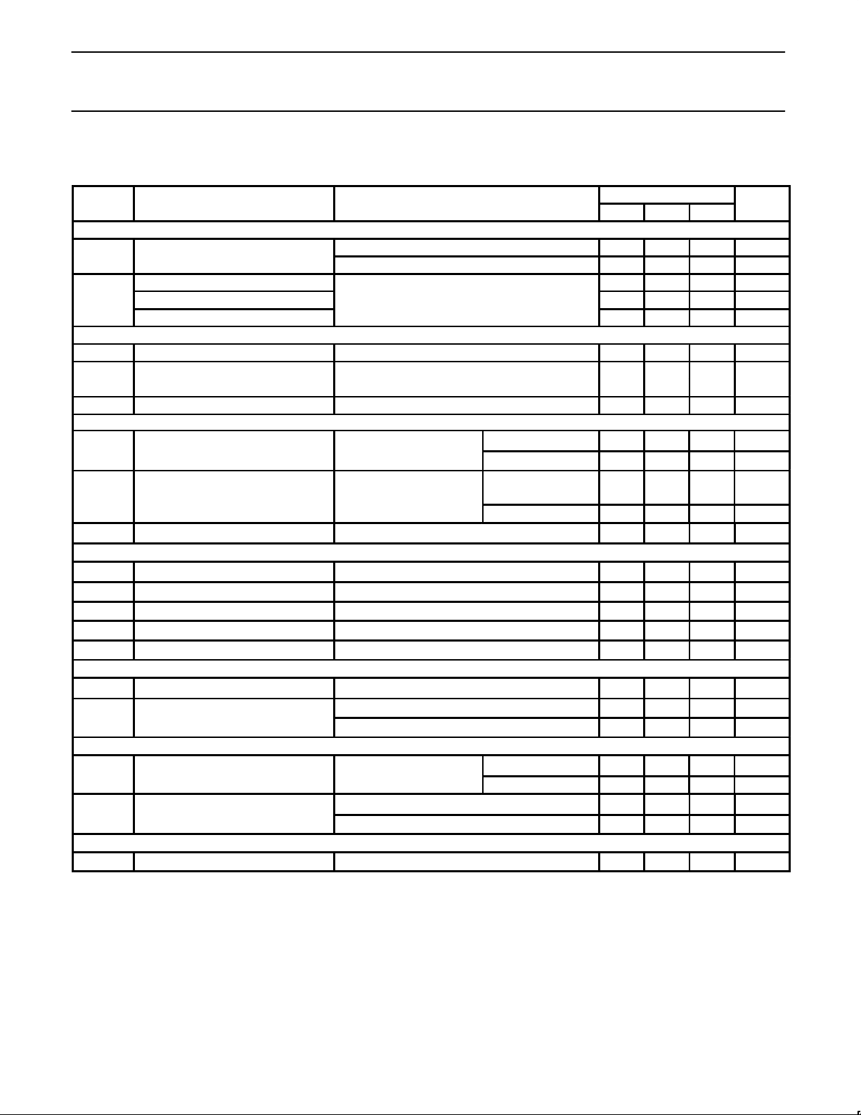
DC ELECTRICAL CHARACTERISTICS
VCC=12V, TA=25°C, unless otherwise specified.
NE5568
SYMBOL
PARAMETER
TEST CONDITIONS
Min Typ Max
UNIT
Reference section
V
REF
Internal reference voltage TA=25°C 3.69 3.75 3.84 V
Over temperature 3.66 3.87 V
V
Z
Internal zener ref 7.8 8.2 8.8 V
Temperature coefficient of V
REF
IL=7mA ± 100 ppm/°C
Temperature coefficient of V
Z
± 200 ppm/°C
Oscillator section
f Frequency range Over temperature 50 100k Hz
Initial accuracy RT and CT Constant 5 %
Duty cycle range fo=20kHz 0 98 %
Current limiting
I
IN
Input current Pin 6=250mV TA=25°C -2 -10 µA
Over temp. -20 µA
Single pulse inhibit delay
Inhibit delay time for
20% overdrive at
I
OUT
=20mA 0.88 1.10 µs
I
OUT
=40mA 0.7 0.8 µs
Current limit trip level 0.400 0.500 0.600 V
Error amplifier
Open-loop gain 60 dB
Feedback resistor 10k Ω
BW Small-signal bandwidth 3 MHz
V
OH
Output voltage swing 6.2 V
V
OL
Output voltage swing 0.7 V
Output stage
I
OUT
Output current Over temperature 20 mA
V
CE
Saturation IC=20mA, over temperature 0.4 V
IC=40mA, over temperature 0.5 V
Supply voltage/current
I
CC
Supply current IZ=0, voltage-fed TA=25°C 10.0 mA
Over temp. 13.0 mA
V
CC
Supply voltage IS=10mA, current-fed 19.0 21.0 24.0 V
ICC=30mA, current-fed 20.0 30.0 V
Low supply protection
Pin 1 threshold 8.0 9.0 10.5 V
NOTES:
All curves and applications of NE5561 apply exactly
 Loading...