

Philips IP4281CZ10 Datasheet

IP4281CZ10
ESD protection for high-speed interfaces
Rev. 01 — 25 September 2008 Product data sheet
1. Product profile
1.1 General description
The IP4281CZ10 is designed for HDMI interface protection. The device includes
high-level ElectroStatic Discharge (ESD) protection diodes for the TMDS signal lines.
All TMDS intra-pairs are protected by a special diode configuration offering a low line
capacitance of only 0.7 pF. These diodes provide protection to downstream components
from ESD voltages up to ±8 kV contact according to IEC 61000-4-2, level 4.
1.2 Features
n Pb-free, RoHS compliant and free of Halogen and Antimony (dark green compliant)
n ESD protection for HDMI and other LVDS data lines
n All TMDS lines with integrated rail-to-rail clamping diodes for downstream ESD
protection of ±8 kV according to IEC61000-4-2, level 4
n Matched 0.5 mm trace spacing
n TMDS lines with ≤ 0.05 pF matching capacitance between TMDS pairs
n Line capacitance of only 0.7 pF for each channel
n 4-channel, 10-terminal Ultra-Thin Leadless Package (UTLP)
n HDMI 1.3a compliant
1.3 Applications
The IP4281CZ10 is designed for HDMI receiver and transmitter port protection:
n TV, monitor
n Notebook, main board graphics card and ports
n Set-top box and game consoles
n DVD recorder and player
NXP Semiconductors
IP4281CZ10
ESD protection for high-speed interfaces
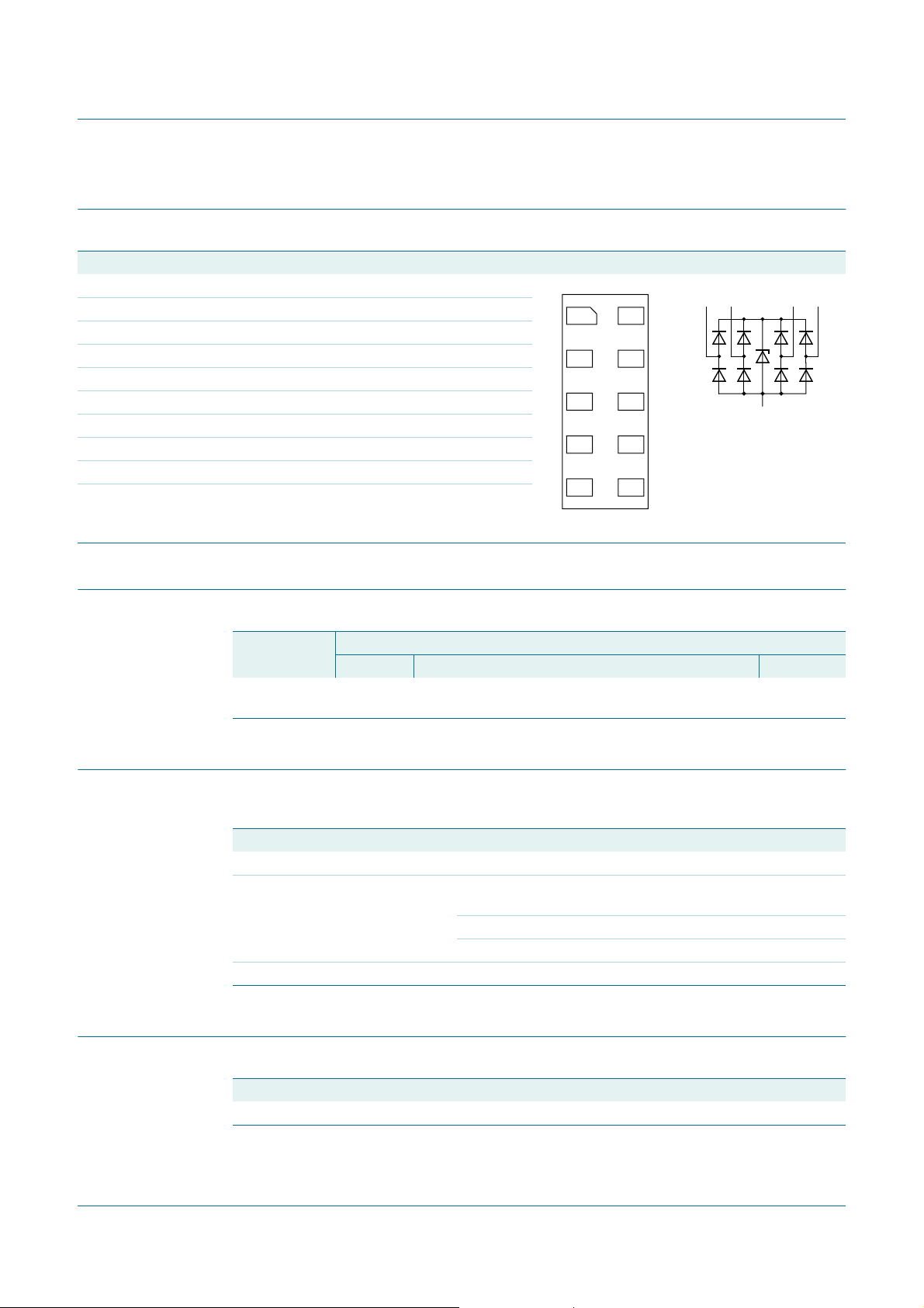
2. Pinning information
Table 1. Pinning
Pin Symbol Description Simplified outline Graphic symbol
1 TMDS_CH1− negative channel 1 ESD protection
2 TMDS_CH1+ positive channel 1 ESD protection
3 GND GND
4 TMDS_CH2− negative channel 2 ESD protection
5 TMDS_CH2+ positive channel 2 ESD protection
6 n.c. not connected
7 n.c. not connected
8 GND GND
9 n.c. not connected
10 n.c. not connected
1
2
3
4
5
Transparent top view
10
9
8
7
6
24
1 5
3, 8
001aai619
3. Ordering information
Table 2. Ordering information
Type number Package
Name Description Version
IP4281CZ10 XSON10U plastic extremely thin small outline package; no leads;
10 terminals; UTLP based; body 1 × 2.5× 0.5 mm
4. Limiting values
Table 3. Limiting values
In accordance with the Absolute Maximum Rating System (IEC 60134).
Symbol Parameter Conditions Min Max Unit
V
I
V
esd
input voltage GND − 0.5 +3.63 V
electrostatic discharge
voltage
all pins to ground;
IEC 61000-4-2, level 4
contact −8+8kV
air discharge −15 +15 kV
T
stg
storage temperature −55 +125 °C
5. Recommended operating conditions
SOT1059-1
Table 4. Operating conditions
Symbol Parameter Conditions Min Max Unit
T
amb
IP4281CZ10_1 © NXP B.V. 2008. All rights reserved.
Product data sheet Rev. 01 — 25 September 2008 2 of 8
ambient temperature −40 +85 °C

NXP Semiconductors
IP4281CZ10
ESD protection for high-speed interfaces
6. Characteristics
Table 5. Characteristics
Symbol Parameter Conditions Min Typ Max Unit
V
BRzd
I
LRzd
V
F
C
ch(TMDS)
∆C
ch(TMDS)
C
ch(mutual)
R
dyn
V
CL(ch)trt(pos)
Zener diode breakdown voltage I = 1 mA 6 - 9 V
Zener diode reverse leakage current per TMDS channel; V = 3.0 V - - 1 µA
forward voltage - 0.7 - V
TMDS channel capacitance f = 1 MHz; V
TMDS channel capacitance difference f = 1 MHz; V
bias
bias
= 2.5 V
= 2.5 V
mutual channel capacitance between signal pin and pin n.c.;
f = 1 MHz; V
dynamic resistance I = 1 A, T
= 2.5 V
bias
= 25 °C; IEC 61000-4-5/9
amb
[1]
- 0.7 - pF
[1]
- 0.05 - pF
[1]
- 0.07 - pF
positive transient - 2.4 - Ω
negative transient - 1.3 - Ω
positive transient channel clamping
V
= 8 kV HBM; T
esd
=25°C-8-V
amb
voltage
[1] This parameter is guaranteed by design.
IP4281CZ10_1 © NXP B.V. 2008. All rights reserved.
Product data sheet Rev. 01 — 25 September 2008 3 of 8
 Loading...