

Philips 74HCT1G14GW, 74HC1G14GW Datasheet

INTEGRATED CIRCUITS
DATA SH EET
74HC1G14; 74HCT1G14
Inverting Schmitt-trigger
Product specification
File under Integrated Circuits, IC06
1998 Aug 05
Philips Semiconductors Product specification
Inverting Schmitt-trigger 74HC1G14; 74HCT1G14
FEATURES
• Wide operating voltage range:
2.0 to 6.0 V
• Symmetrical output impedance
• High noise immunity
• Low power dissipation
• Balanced propagation delays
• Very small 5 pins package
• Applications
– Wave and pulse shapers
– Astable multivibrators
– Monostable multivibrators
• Output capability: standard.
DESCRIPTION
The 74HC1G/HCT1G14 is a
high-speed Si-gate CMOS device.
The 74HC1G/HCT1G14 provides the
inverting buffer function with
Schmitt-trigger action. These devices
are capable of transforming slowly
changing input signals into sharply
defined, jitter-free output signals.
1
The standard output currents are
⁄
2
compared to the 74HC/HCT14.
FUNCTION TABLE
See note 1.
INPUT
inA
OUTPUT
outY
LH
HL
QUICK REFERENCE DATA
GND = 0 V; T
=25°C; tr=tf= 6.0 ns.
amb
SYMBOL PARAMETER CONDITIONS
t
PHL/tPLH
C
I
propagation
delay inA to outY
input
CL=15pF
VCC=5V
capacitance
C
PD
power
notes 1 and 2 20 22 pF
dissipation
capacitance
Notes
1. C
is used to determine the dynamic power dissipation (PDin µW).
PD
PD=CPD× V
2
× fi+ ∑ (CL× V
CC
2
× fo) where:
CC
fi= input frequency in MHz;
fo= output frequency in MHz;
CL= output load capacitance in pF;
VCC= supply voltage in V;
∑ (CL× V
2. For HC1G the condition is VI= GND to V
2
× fo) = sum of outputs.
CC
CC.
For HCT1G the condition is VI= GND to VCC− 1.5 V.
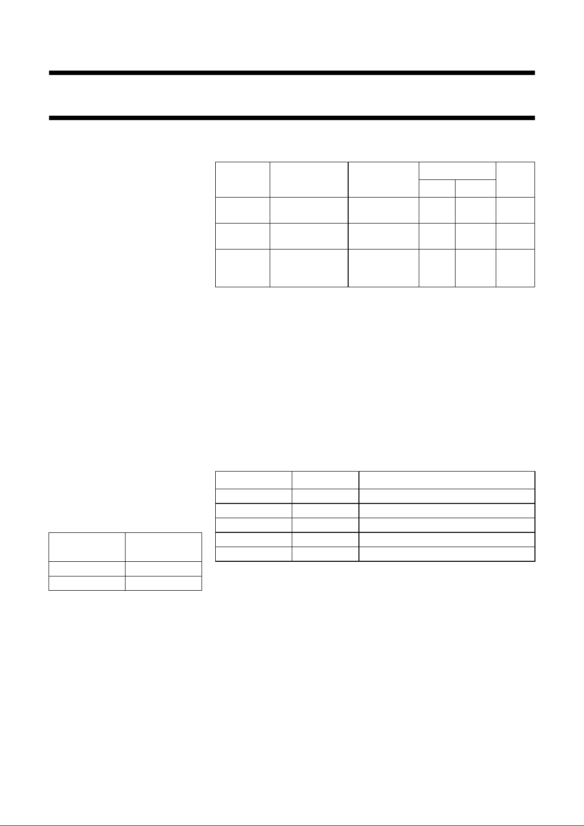
PINNING
PIN SYMBOL DESCRIPTION
1 n.c. not connected
2 inA data input
3 GND ground (0 V)
4 outY data output
5V
CC
DC supply voltage
TYP.
UNIT
HC1G HCT1G
10 15 ns
1.5 1.5 pF
Note
1. H = HIGH voltage level;
L = LOW voltage level.
1998 Aug 05 2
Philips Semiconductors Product specification
Inverting Schmitt-trigger 74HC1G14; 74HCT1G14
ORDERING AND PACKAGE INFORMATION
OUTSIDE NORTH
PACKAGES
AMERICA
74HC1G14GW
74HCT1G14GW 5 SC-88A plastic SOT353 TF
handbook, halfpage
n.c
inA
GND
TEMPERATURE
−40 to +125 °C
1
2
14
3
MNA022
RANGE
V
5
outY
4
CC
PINS PACKAGE MATERIAL CODE MARKING
5 SC-88A plastic SOT353 HF
handbook, halfpage
inA outY
2
4
MNA023
handbook, halfpage
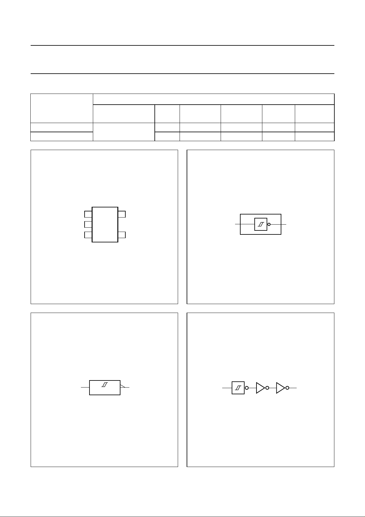
Fig.1 Pin configuration.
24
MNA024
Fig.3 IEC logic symbol.
handbook, halfpage
inA
Fig.2 Logic symbol.
outY
MNA025
Fig.4 Logic diagram.
1998 Aug 05 3
Philips Semiconductors Product specification
Inverting Schmitt-trigger 74HC1G14; 74HCT1G14
RECOMMENDED OPERATING CONDITIONS
SYMBOL PARAMETER
UNIT CONDITIONS
MIN. TYP. MAX. MIN. TYP. MAX.
74HC1G 74HCT1G
V
CC
V
I
V
O
T
amb
DC supply voltage 2.0 5.0 6.0 4.5 5.0 5.5 V
input voltage 0 − V
output voltage 0 − V
operating ambient
−40 +25 +125 −40 +25 +125 °C see DC and AC
0 − V
CC
0 − V
CC
CC
CC
temperature range
V
V
characteristics per device
LIMITING VALUES
In accordance with the Absolute Maximum Rating System (IEC 134); voltages are referenced to GND (ground = 0 V).
SYMBOL P ARAMETER CONDITIONS MIN. MAX. UNIT
V
CC
±I
IK
±I
OK
±I
O
DC supply voltage −0.5 +7.0 V
DC input diode current VI<−0.5 or VI> VCC+ 0.5 V; note 1 − 20 mA
DC output diode current VO<−0.5 or VO> VCC+ 0.5 V; note 1 − 20 mA
DC output source or sink
−0.5 V < VO< VCC+ 0.5 V; note 1 − 12.5 mA
current standard outputs
±I
CC
DC VCC or GND current for
note 1 − 25 mA
types with standard outputs
T
stg
P
D
storage temperature range −65 +150 °C
power dissipation per package for temperature range: −40 to +125 °C
5 pins plastic SC-88A above +55 °C derate linearly with
− 200 mW
2.5 mW/K
Note
1. The input and output voltage ratings may be exceeded if the input and output current ratings are observed.
1998 Aug 05 4
Philips Semiconductors Product specification
Inverting Schmitt-trigger 74HC1G14; 74HCT1G14
DC CHARACTERISTICS FOR THE 74HC1G
Over recommended operating conditions; voltages are referenced to GND (ground = 0 V).
T
SYMBOL PARAMETER
V
OH
HIGH-level output
voltage; all outputs
V
OH
HIGH-level output
voltage; standard
outputs
V
OL
LOW-level output
voltage; all outputs
V
OL
LOW-level output
voltage; standard
outputs
I
I
I
CC
input leakage current −− 1.0 − 1.0 µA 6.0 VI=VCCor GND
quiescent supply
current
(°C)
amb
−40 to +85 −40 to +125
MIN. TYP.
(1)
MAX. MIN. MAX.
UNIT
1.9 2.0 − 1.9 − V 2.0 VI=VIHor VIL;
4.4 4.5 − 4.4 − V 4.5
5.9 6.0 − 5.9 − V 6.0
4.13 4.32 − 3.7 − V 4.5 VI=VIHor VIL;
5.63 5.81 − 5.2 − V 6.0 V
− 0 0.1 − 0.1 V 2.0 VI=VIHor VIL;
− 0 0.1 − 0.1 V 4.5
− 0 0.1 − 0.1 V 6.0
− 0.15 0.33 − 0.4 V 4.5 VI=VIHor VIL;
− 0.16 0.33 − 0.4 V 6.0 V
−− 10 − 20 µA 6.0 VI=VCCor GND;
TEST CONDITIONS
VCC (V) OTHER
−IO=20µA
−IO= 2.0 mA
or VIL;
I=VIH
−IO= 2.6 mA
IO=20µA
IO= 2.0 mA
or VIL;
I=VIH
IO= 2.6 mA
IO=0
Note
1. All typical values are measured at T
amb
=25°C.
DC CHARACTERISTICS FOR THE 74HC1G14
Voltages are referenced to GND (ground = 0 V).
SYMBOL PARAMETER
MIN. TYP.
V
T+
positive-going threshold 0.7 1.09 1.5 0.7 1.5 V 2.0 see Figs 5 and 6
1.7 2.36 3.15 1.7 3.15 V 4.5
2.1 3.12 4.2 2.1 4.2 V 6.0
V
T−
negative-going threshold 0.3 0.60 0.9 0.3 0.9 V 2.0 see Figs 5 and 6
0.9 1.53 2.0 0.9 2.0 V 4.5
1.2 2.08 2.6 1.2 2.6 V 6.0
V
H
hysteresis (VT+− VT−) 0.2 0.48 1.0 0.2 1.0 V 2.0 see Figs 5 and 6
0.4 0.83 1.4 0.4 1.4 V 4.5
0.6 1.04 1.6 0.6 1.6 V 6.0
Note
1. All typical values are measured at T
amb
=25°C.
T
(°C)
amb
−40 to +85 −40 to +125
(1)
MAX. MIN. MAX.
TEST CONDITIONS
UNIT
VCC (V) WAVEFORMS
1998 Aug 05 5
 Loading...