

Panasonic UNR4111, UNR4112, UNR4113, UNR4114, UNR4115 Technical data
...
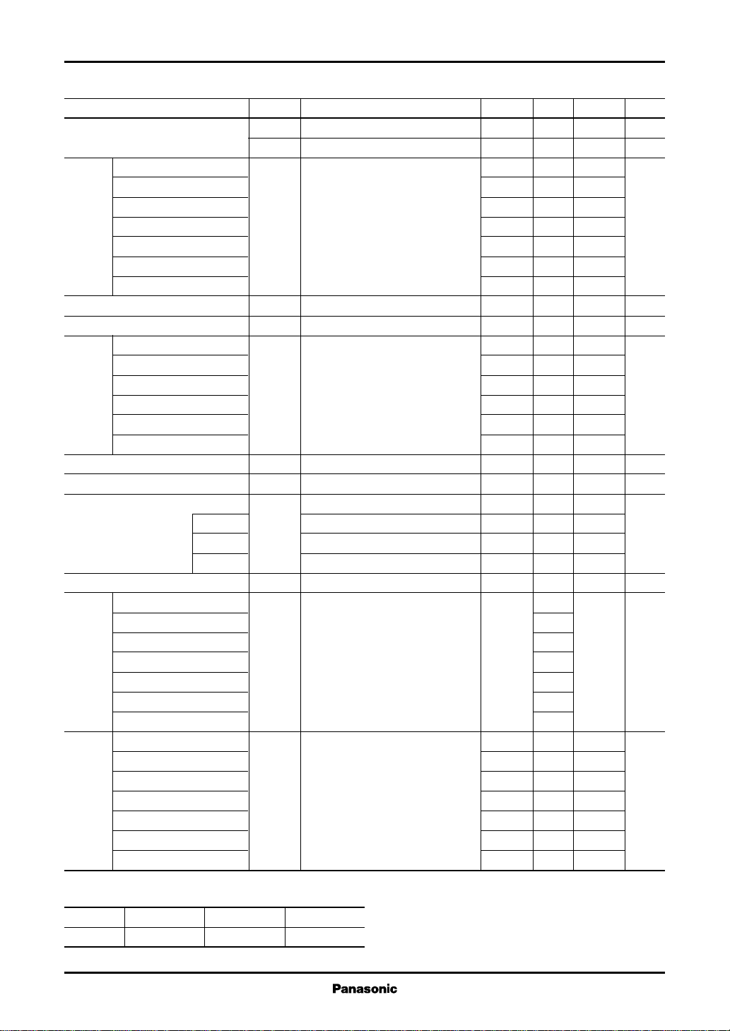
Transistors with built-in Resistor
B
C
R1
R2
E
UNR4111/4112/4113/4114/4115/4116/4117/
4118/4119/4110/411D/411E/411F/411H/411L
(UN4111/4112/4113/4114/4115/4116/4117/4118/
4119/4110/411D/411E/411F/411H/411L)
Silicon PNP epitaxial planer transistor
For digital circuits
Features
■
●
Costs can be reduced through downsizing of the equipment and
reduction of the number of parts.
●
New S type package, allowing supply with the radial taping.
Resistance by Part Number
■
(R1)(R
●
UNR411 1 10kΩ 10kΩ
●
UNR4112 22kΩ 22kΩ
●
UNR4113 47kΩ 47kΩ
●
UNR4114 10kΩ 47kΩ
●
UNR4115 10kΩ —
●
UNR4116 4.7kΩ —
●
UNR4117 22kΩ —
●
UNR4118 0.51kΩ 5.1kΩ
●
UNR4119 1kΩ 10kΩ
●
UNR4110 47kΩ —
●
UNR411D 47kΩ 10kΩ
●
UNR411E 47kΩ 22kΩ
●
UNR411F 4.7kΩ 10kΩ
●
UNR411H 2.2kΩ 10kΩ
●
UNR411L 4.7kΩ 4.7kΩ
)
2
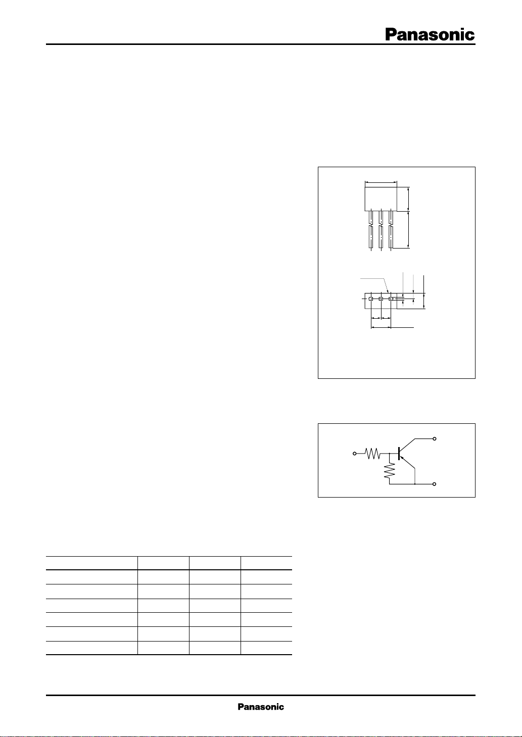
4.0±0.2
marking
123
1.271.27
Internal Connection
3.0±0.215.6±0.5
0.1
+0.2
–
0.7±0.1
0.45
2.0±0.2
2.54±0.15
1 : Emitter
2 : Collector
3 : Base
New S Type Package
Unit: mm
Absolute Maximum Ratings (Ta=25˚C)
■
Parameter Symbol Ratings Unit
Collector to base voltage V
Collector to emitter voltage
Collector current I
Total power dissipation P
Junction temperature T
Storage temperature T
CBO
V
CEO
C
T
j
stg
–50 V
–50 V
–100 mA
300 mW
150 ˚C
–55 to +150 ˚C
Note)The part numbers in the parenthesis show conventional part number.
1
UNR4111/4112/4113/4114/4115/4116/4117/4118/
Transistors with built-in Resistor
Electrical Characteristics (Ta=25˚C)
■
Parameter Symbol Conditions min typ max Unit
I
Collector cutoff current
I
CBO
CEO
UNR411 1 – 0.5
UNR4112/4114/411E/411D – 0.2
Emitter
cutoff
current
UNR4113 – 0.1
UNR4115/4116/4117/4110 I
EBO
UNR411F/411H –1.0
UNR4119 –1.5
UNR4118/411L –2.0
Collector to base voltage V
Collector to emitter voltage V
CBO
CEO
UNR411 1 35
UNR4112/411E 60
Forward
current
transfer
ratio
UNR4113/4114
UNR4115*/41 16*/4117*/4110*
h
FE
UNR411F/411D/4119/411H 30
UNR4118/411L 20
Collector to emitter saturation voltage V
Output voltage high level V
CE(sat)IC
OH
Output voltage low level VCC = –5V, VB = –2.5V, RL = 1kΩ – 0.2
UNR4113
UNR411D VCC = –5V, VB = –10V, RL = 1kΩ – 0.2
V
OL
UNR411E VCC = 5V, VB = –6V, RL = 1kΩ – 0.2
Transition frequency f
T
UNR4111/4114/4115 10
UNR4112/4117 22
UNR4113/4110/411D/411E 47
Input
resistance
UNR4116/411F/411L R
1
UNR4118 0.51
UNR4119 1
UNR411H 2.2
UNR4111/4112/4113/411L 0.8 1.0 1.2
UNR4114 0.17 0.21 0.25
UNR4118/4119 0.08 0.1 0.12
Resistance
ratio
UNR411D R1/R
UNR411E 1.7 2.14 2.6
UNR411F 0.37 0.47 0.57
UNR411H 0.17 0.22 0.27
VCB = –50V, IE = 0 – 0.1 µA
VCE = –50V, IB = 0 – 0.5 µA
VEB = –6V, IC = 0 – 0.01 mA
IC = –10µA, IE = 0 –50 V
IC = –2mA, IB = 0 –50 V
VCE = –10V, IC = –5mA
= –10mA, IB = – 0.3mA – 0.25 V
VCC = –5V, VB = – 0.5V, RL = 1kΩ –4.9 V
VCC = –5V, VB = –3.5V, RL = 1kΩ – 0.2
VCB = –10V, IE = 1mA, f = 200MHz 80 MHz
2
4119/4110/411D/411E/411F/411H/411L
80
160 460
(–30%) 4.7 (+30%) kΩ
3.7 4.7 5.7
V
* hFE rank classification (UNR4115/4116/4117/4110)
Rank Q R S
h
FE
160 to 260 210 to 340 290 to 460
2
UNR4111/4112/4113/4114/4115/4116/4117/4118/
Transistors with built-in Resistor
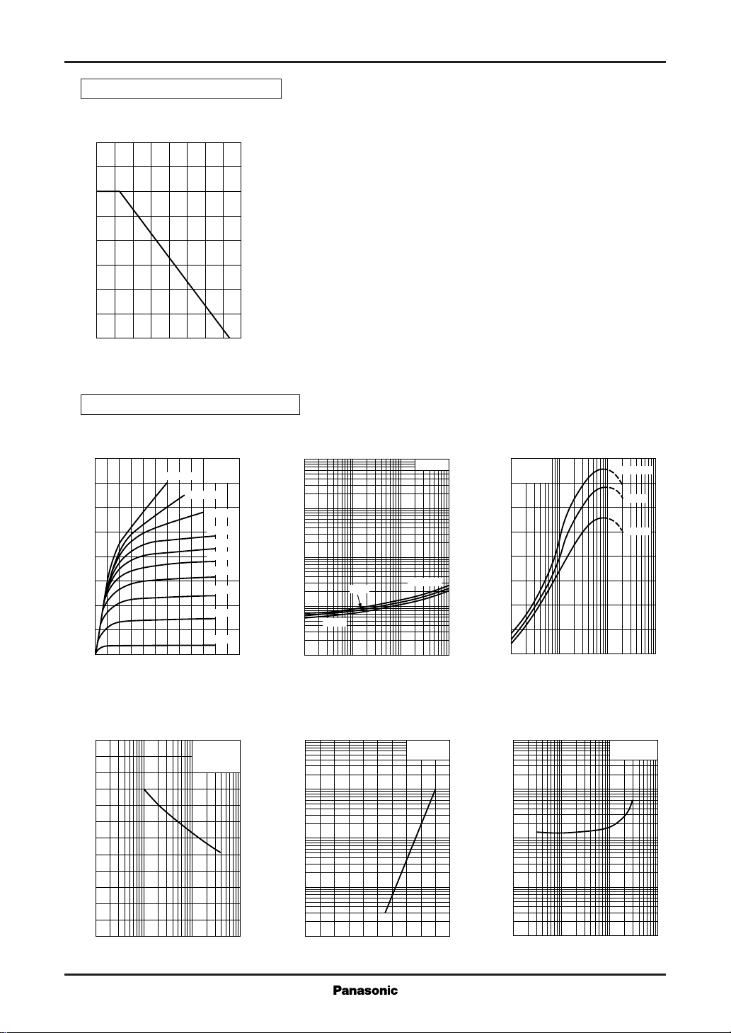
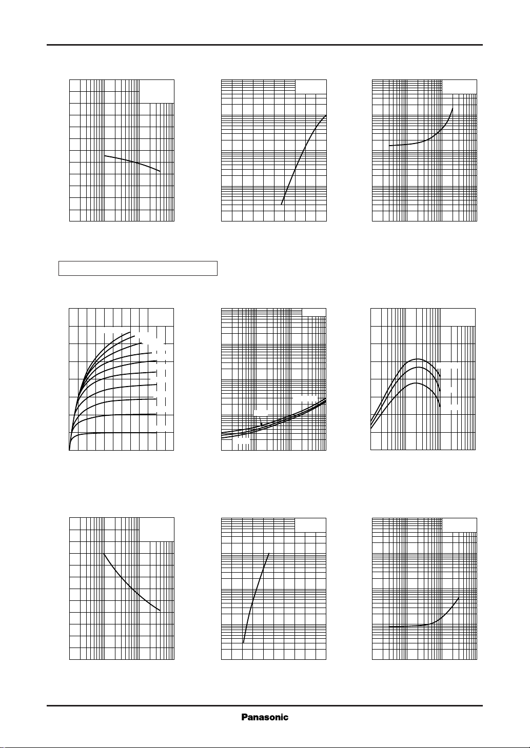
Common characteristics chart
— Ta
P
T
400
)
mW
(
300
T
200
100
Total power dissipation P
0
0 16020 60 100 14040 12080
Ambient temperature Ta (˚C
Characteristics charts of UNR4111
)
4119/4110/411D/411E/411F/411H/411L
— V
I
C
–160
–140
)
–120
mA
(
C
–100
–80
–60
–40
Collector current I
–20
0
0 –12–2 –10–4 –8–6
Collector to emitter voltage VCE (V
Cob — V
6
)
pF
(
5
ob
4
3
CE
IB=–1.0mA
CB
–0.9mA
f=1MHz
I
E
Ta=25˚C
Ta=25˚C
–0.8mA
–0.7mA
–0.6mA
–0.5mA
–0.4mA
–0.3mA
–0.2mA
–0.1mA
=0
V
— I
CE(sat)
–100
)
V
(
–30
CE(sat)
–10
–3
–1
–0.3
–0.1
–0.03
Collector to emitter saturation voltage V
–0.01
–0.1 –0.3
)
25˚C
–25˚C
–1 –3 –10 –30 –100
Collector current IC (mA
IO — V
–10000
–3000
)
–1000
µA
(
O
–300
–100
C
IC/IB=10
Ta=75˚C
160
FE
120
80
40
Forward current transfer ratio h
0
–1 –3
)
IN
)
V
(
IN
–100
–30
–10
–3
–1
VO=–5V
Ta=25˚C
hFE — I
C
VCE=–10V
–10 –30 –100 –300 –1000
Collector current IC (mA
VIN — I
O
Ta=75˚C
25˚C
–25˚C
)
VO=–0.2V
Ta=25˚C
2
1
Collector output capacitance C
0
–0.1 –0.3
–1 –3 –10 –30 –100
Collector to base voltage VCB (V
–30
–10
Output current I
–
3
–1
–0.4
)
Input voltage VIN (V
–1.4–1.2–1.0–0.8–0.6
)
–0.3
Input voltage V
–0.1
–0.03
–0.01
–0.1 –0.3
Output current IO (mA
–1 –3 –10 –30 –100
)
3
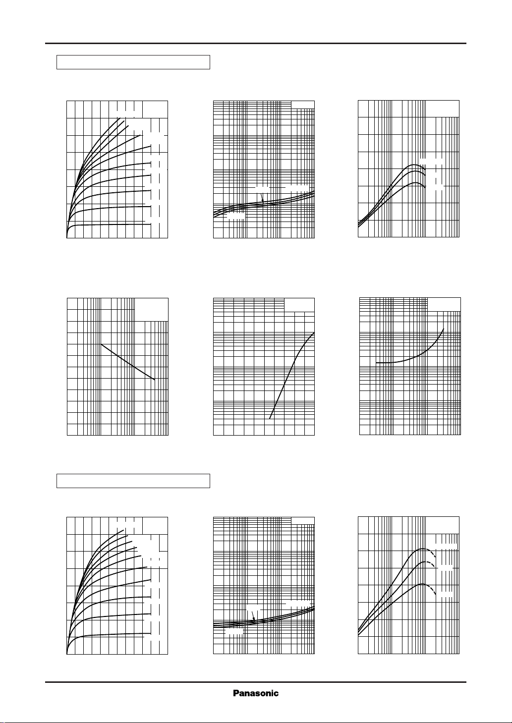
UNR4111/4112/4113/4114/4115/4116/4117/4118/
Transistors with built-in Resistor
Characteristics charts of UNR4112
4119/4110/411D/411E/411F/411H/411L
— V
I
C
–160
–140
)
–120
mA
(
C
–100
–80
–60
–40
Collector current I
–20
0
0 –12–2 –10–4 –8–6
Collector to emitter voltage VCE (V
Cob — V
6
)
pF
(
5
ob
4
3
CE
IB=–1.0mA
–0.9mA
CB
–0.8mA
f=1MHz
I
E
Ta=25˚C
Ta=25˚C
–0.7mA
–0.6mA
–0.5mA
–0.4mA
–0.3mA
–0.2mA
–0.1mA
=0
V
— I
CE(sat)
–100
)
V
(
–30
CE(sat)
–10
–3
–1
–0.3
–0.1
–0.03
Collector to emitter saturation voltage V
–0.01
)
–25˚C
–0.1 –0.3
–1 –3 –10 –30 –100
Collector current IC (mA
IO — V
–10000
–3000
)
–1000
µA
(
O
–300
–100
25˚C
C
IC/IB=10
Ta=75˚C
400
FE
300
200
100
Forward current transfer ratio h
0
–1 –3
)
IN
)
V
(
IN
–100
–30
–10
–3
–1
VO=–5V
Ta=25˚C
hFE — I
C
VCE=–10V
Ta=75˚C
25˚C
–25˚C
–10 –30 –100 –300 –1000
Collector current IC (mA
VIN — I
O
VO=–0.2V
Ta=25˚C
)
2
1
Collector output capacitance C
0
–0.1 –0.3
–1 –3 –10 –30 –100
Collector to base voltage VCB (V
Characteristics charts of UNR4113
— V
I
C
–160
–140
)
–120
mA
(
C
–100
–80
–60
–40
Collector current I
–20
0
0 –12–2 –10–4 –8–6
Collector to emitter voltage VCE (V
CE
IB=–1.0mA
–0.9mA
–0.8mA
–0.7mA
Ta=25˚C
–0.6mA
–0.5mA
–0.4mA
–0.3mA
–0.2mA
–0.1mA
)
–30
–10
Output current I
–3
–1
–0.4
)
–100
)
V
(
CE(sat)
–0.03
Collector to emitter saturation voltage V
–0.01
Input voltage VIN (V
–30
–10
–3
–1
–0.3
–0.1
–25˚C
–0.1 –0.3
V
— I
CE(sat)
25˚C
–1 –3 –10 –30 –100
Collector current IC (mA
–1.4–1.2–1.0–0.8–0.6
)
C
IC/IB=10
Ta=75˚C
)
–0.3
Input voltage V
–0.1
–0.03
–0.01
–0.1 –0.3
–1 –3 –10 –30 –100
Output current IO (mA
hFE — I
400
FE
300
200
100
C
VCE=–10V
Forward current transfer ratio h
0
–1 –3
–10 –30 –100 –300 –1000
Collector current IC (mA
)
Ta=75˚C
25˚C
–25˚C
)
4
UNR4111/4112/4113/4114/4115/4116/4117/4118/
Transistors with built-in Resistor
4119/4110/411D/411E/411F/411H/411L
)
pF
(
Cob — V
6
5
ob
4
3
2
1
CB
f=1MHz
I
=0
E
Ta=25˚C
Collector output capacitance C
0
–0.1 –0.3
–1 –3 –10 –30 –100
Collector to base voltage VCB (V
Characteristics charts of UNR4114
— V
I
C
CE
–160
–140
)
–120
mA
(
C
–100
–80
–60
–40
Collector current I
–20
0
IB=–1.0mA
0 –12–2 –10–4 –8–6
Collector to emitter voltage VCE (V
Ta=25˚C
–0.9mA
–0.8mA
–0.7mA
–0.6mA
–0.5mA
–0.4mA
–0.3mA
–0.2mA
–0.1mA
)
IO — V
IN
–10000
–3000
)
–1000
µA
(
O
–300
–100
–30
–10
Output current I
–3
–1
–0.4
)
–100
)
V
(
CE(sat)
–0.03
Collector to emitter saturation voltage V
–0.01
Input voltage VIN (V
–30
–10
–3
–1
–0.3
–0.1
–25˚C
–0.1 –0.3
V
CE(sat)
25˚C
–1 –3 –10 –30 –100
Collector current IC (mA
— I
VO=–5V
Ta=25˚C
C
Ta=75˚C
–1.4–1.2–1.0–0.8–0.6
)
IC/IB=10
)
–100
–30
)
–10
V
(
IN
–3
–1
–0.3
Input voltage V
–0.1
–0.03
–0.01
–0.1 –0.3
400
FE
300
200
100
Forward current transfer ratio h
0
–1 –3
VIN — I
O
VO=–0.2V
Ta=25˚C
–1 –3 –10 –30 –100
Output current IO (mA
hFE — I
C
VCE=–10V
Ta=75˚C
25˚C
–25˚C
–10 –30 –100 –300 –1000
Collector current IC (mA
)
)
)
pF
(
Cob — V
6
5
ob
4
3
2
1
CB
Collector output capacitance C
0
–0.1 –0.3
–1 –3 –10 –30 –100
Collector to base voltage VCB (V
f=1MHz
=0
I
E
Ta=25˚C
IO — V
IN
–10000
–3000
)
–1000
µA
(
O
–300
–100
–30
–10
Output current I
–3
–1
–0.4
)
Input voltage VIN (V
VO=–5V
Ta=25˚C
)
–1.4–1.2–1.0–0.8–0.6
–1000
–300
)
–100
V
(
IN
–30
–10
–3
Input voltage V
–1
–0.3
–0.1
–0.1 –0.3
VIN — I
O
VO=–0.2V
Ta=25˚C
–1 –3 –10 –30 –100
Output current IO (mA
)
5
 Loading...