

Page 1

Optic Touch Panel
A
TY-TP42P8-S
TY-TP50P8-S
TY-TPEN6 (Option)
ORDER NO. ITD0510062CE
D18
Specifications
Power Source
Voltage DC + 5V ± 10 %
Electric current DC + 5V Max400 m
Supplysystem from USB Bus Power (DC + 5V Max500 mA)
Touch Panel
Detection system Infrared obstruction detection system
Panel window (W × H) 945.2 mm × 531.2 mm (37.2” × 20.9”)
(TY-TP42P8-S)
Detection range (W × H) 920 mm × 516 mm (36.2” × 20.3”)
(TY-TP42P8-S)
Effective detection range Detection range + 1.0 mm (0.04”) at the top, bottom, left and right
Operating modes Detection operation at input point, during initial movement and at end point *1
Resolution (W × H) 1,841 × 1,033 *1 (TY-TP42P8-S) 2,209 × 1,241 *1 (TY-TP50P8-S)
Detection pitch 2.0 mm × 2.0 mm (0.08” × 0.08”)
Output system Coordinate output
Number of optic elements (W × H) 231 × 130 elements (TY-TP42P8-S) 277 × 156 elements (TY-TP50P8-S)
Optic element pitch (W × H) 4.0 mm × 4.0 mm (0.16” × 0.16”)
1129.2 mm × 645.2 mm (44.4” × 25.4”)
(TY-TP50P8-S)
1104 mm × 620 mm (43.4” × 24.4”)
(TY-TP50P8-S)
© 2005 Matsushita Electric Industrial Co., Ltd. All
rights reserved. Unauthorized copying and
distribution is a violation of law.
Page 2
y
t
t
A
TY-TP42P8-S / TY-TP50P8-S
Minimum stylus size (W × H) 6.0 mm × 6.0 mm (0.24” × 0.24”)
Scan speed Initial touch: 30 ms/frame max.; during movement: 8 ms/frame max.
Touch pen Infrared system
USB Interface (USB 1.1) Terminal No. and Signal name
(TYPE B)
No.1 Vcc No.2 -DATA
No.3 +DATA No.4 GND
Temperature When operating 0°C (32°F) to 50°C (122°F) (temperature gradient 25°C (77°F)/hrmax.) *2
When not operating: -20°C (-4°F) to 60° (140°F) temperature gradient 25°C (77°F)/hr max.
Humidit
Resistance to extraneous ligh
Panel form Flat panel (Flat type)
External dimensions (W×H×T) 1,073 mm × 659 mm × 69 mm
Weigh
Extruded material
When operating: 20% to 85% (must be no condensation) *2
When not operating: 10% to 95%
Lateral light: 2,000 lux MIN +20% (angle of incidence: 20°)
Frontal light: 10,000 lux MIN +20% (angle of incidence: 90°)
1,257 mm × 773 mm × 69 mm
(42.2” × 25.9” × 2.7”)
(Excluding mounting brackets)
(TY-TP42P8-S)
5.0 kg (11 lbs) Excluding mounting brackets
(TY-TP42P8-S)
luminum
(49.5” × 30.4” × 2.7”)
(Excluding mounting brackets)
(TY-TP50P8-S)
5.8 kg (12.7 lbs) Excluding mounting brackets
(TY-TP50P8-S)
Notes:
*1*2When it is used with exclusive driver software.
This applies to the touch panel alone. When the panel is attached to a device such as a PDP, follow the environmental conditions for the
device being used.
CONTENTS
Page Page
1 Prevention of Electro Static Discharge (ESD) to
Electrostatically Sensitive (ES) Devices
2 About lead free solder (PbF)
3 External dimensions
4 Setup for Touch Panel
5 Touch Pen (Option)
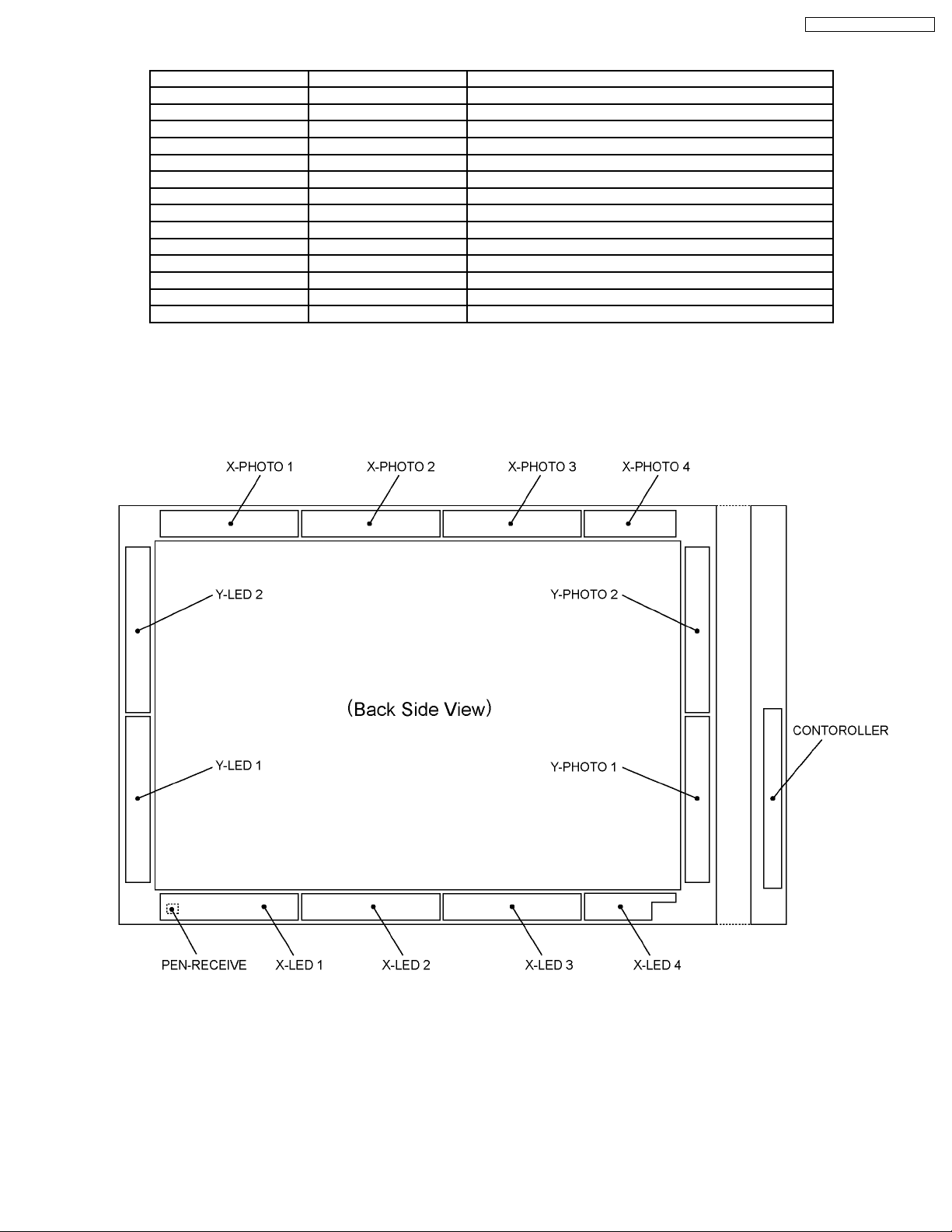
6 Printed Circuit Board Structure
6.1. TY-TP42P8-S
6.2. TY-TP50P8-S
7 Trouble shooting
7.1. Checking procedures
7.2. Test Program
8 Conductor Views
8.1. X-Photo1, X-Photo2, Y-Photo1 Board (42inch)
8.2. X-Photo1, X-Photo2, X-Photo3, Y-Photo1, Y-Photo2 Board
(50inch)
8.3. X-Photo3 Board (42inch)
8.4. X-Photo4 Board (50inch)
8.5. Y-Photo2 Board (42inch)
8.6. X-LED1, X-LED2, Y-LED1 Board (42inch)
4
5
6
7
21
22
22
23
24
24
26
35
35
36
37
38
39
40
8.7. X-LED1, X-LED2, X-LED3, Y-LED1, Y-LED2 Board
(50inch)
8.8. X-LED3 Board (42inch)
8.9. X-LED4 Board (50inch)
8.10. Y-LED2 Board (42inch)
8.11. Controller Board (42inch)
8.12. Controller Board (50inch)
8.13. Pen-Receive Board (42inch)
8.14. Pen-Receive Board (50inch)
9 Block Diagram
9.1. Overall Block Diagram (TY-TP42P8-S)
9.2. Overall Block Diagram (TY-TP50P8-S)
9.3. Detail Block Diagram (1 of 3)
9.4. Detail Block Diagram (2 of 3)
9.5. Detail Block Diagram (3 of 3)
10 Schematic Diagram
10.1. Controller Board Schematic Diagram
10.2. X-Photo 1 Board Schematic Diagram
10.3. X-Photo 2 Board Schematic Diagram
10.4. X-Photo 3 Board Schematic Diagram
41
42
43
44
45
46
47
48
49
49
50
51
52
53
55
55
56
57
58
2
Page 3

10.5. X-Photo 4 Board Schematic Diagram (TY-TP50P8-S) 59
10.6. X-LED 1 Board and Pen Receive Board Schematic
Diagram
10.7. X-LED 2 Board Board Schematic Diagram
10.8. X-LED 3 Board Board Schematic Diagram
60
61
62
10.9. X-LED 4 Board Board Schematic Diagram (TY-TP50P8-S)
10.10. Y-Photo 1 Board Schematic Diagram
10.11. Y-Photo 2 Board Schematic Diagram
10.12. Y-LED 1 Board Schematic Diagram
63
64
65
66
TY-TP42P8-S / TY-TP50P8-S
10.13. Y-LED 2 Board Schematic Diagram 67
11 Exploded View
11.1. TY-TP42P8-S
11.2. TY-TP50P8-S
12 Replacement Parts List
12.1. Replacement Parts List Notes
12.2. TY-TP42P8-S Mechanical Replacement parts List
12.3. TY-TP42P8-S Electrical Replacement parts List
12.4. TY-TP50P8-S Mechanical Replacement parts List
12.5. TY-TP50P8-S Electrical Replacement parts List
69
69
71
73
73
74
75
84
85
3
Page 4
TY-TP42P8-S / TY-TP50P8-S
1 Prevention of Electro Static Discharge (ESD) to
Electrostatically Sensitive (ES) Devices
Some semiconductor (solid state) devices can be damaged easily by static electricity. Such components commonly are called
Electrostatically Sensitive (ES) Devices. Examples of typical ES devices are integrated circuits and some field-effect transistors and
semiconductor "chip" components. The following techniques should be used to help reduce the incidence of component damage
caused by electro static discharge (ESD).
1. Immediately before handling any semiconductor component or semiconductor-equipped assembly, drain off any ESD on your
body by touching a known earth ground. Alternatively, obtain and wear a commercially available discharging ESD wrist strap,
which should be removed for potential shock reasons prior to applying power to the unit under test.
2. After removing an electrical assembly equipped with ES devices, place the assembly on a conductive surface such as
aluminum foil, to prevent electrostatic charge buildup or exposure of the assembly.
3. Use only a grounded-tip soldering iron to solder or unsolder ES devices.
4. Use only an anti-static solder removal device. Some solder removal devices not classified as "anti-static (ESD protected)" can
generate electrical charge sufficient to damage ES devices.
5. Do not use freon-propelled chemicals. These can generate electrical charges sufficient to damage ES devices.
6. Do not remove a replacement ES device from its protective package until immediately before you are ready to install it. (Most
replacement ES devices are packaged with leads electrically shorted together by conductive foam, aluminum foil or comparable
conductive material).
7. Immediately before removing the protective material from the leads of a replacement ES device, touch the protective material
to the chassis or circuit assembly into which the device will be installed.
Caution
Be sure no power is applied to the chassis or circuit, and observe all other safety precautions.
8. Minimize bodily motions when handling unpackaged replacement ES devices. (Otherwise harmless motion such as the
brushing together of your clothes fabric or the lifting of your foot from a carpeted floor can generate static electricity (ESD)
sufficient to damage an ES device).
4
Page 5
TY-TP42P8-S / TY-TP50P8-S
2 About lead free solder (PbF)
Note:
Lead is listed as (Pb) in the periodic table of elements.
In the information below, Pb will refer to Lead solder, and PbF will refer to Lead Free Solder.
The Lead Free Solder used in our manufacturing process and discussed below is (Sn+Ag+Cu).
That is Tin (Sn), Silver (Ag) and Copper (Cu) although other types are available.
This model uses Pb Free solder in it´s manufacture due to environmental conservation issues. For service and repair work, we´d
suggest the use of Pb free solder as well, although Pb solder may be used.
Caution
· Pb free solder has a higher melting point than standard solder. Typically the melting point is 50 ~ 70 °F (30~40 °C) higher.
Please use a high temperature soldering iron and set it to 700 ± 20 °F (370 ± 10 °C).
· Pb free solder will tend to splash when heated too high (about 1100 °F or 600 °C).
If you must use Pb solder, please completely remove all of the Pb free solder on the pins or solder area before applying Pb
solder. If this is not practical, be sure to heat the Pb free solder until it melts, before applying Pb solder.
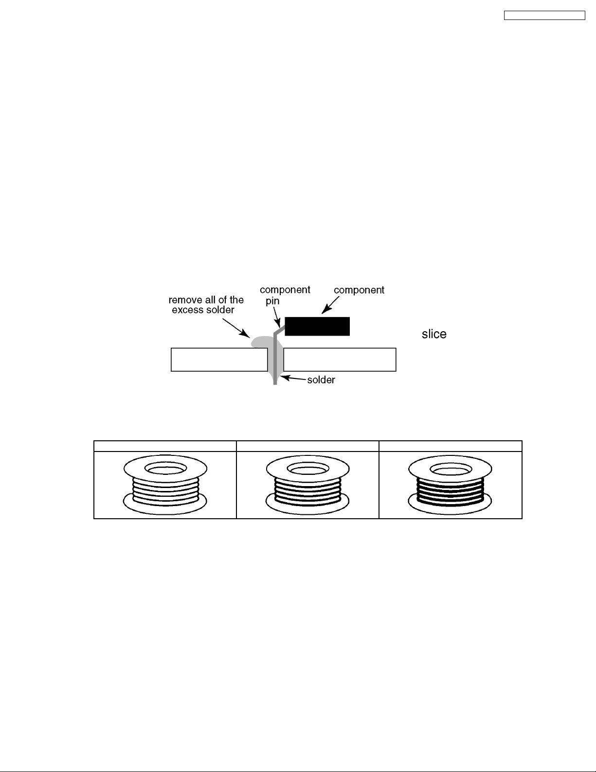
· After applying PbF solder to double layered boards, please check the component side for excess solder which may flow onto
the opposite side. (see figure below)
Suggested Pb free solder
There are several kinds of Pb free solder available for purchase. This product uses Sn+Ag+Cu (tin, silver, copper) solder.
However, Sn+Cu (tin, copper), Sn+Zn+Bi (tin, zinc, bismuth) solder can also be used.
0.3mm x 100g 0.6mm x 100g 1.0mm x 100g
5
Page 6
TY-TP42P8-S / TY-TP50P8-S
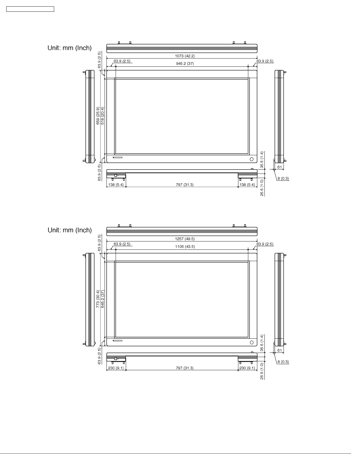
3 External dimensions
TY-TP42P8-S
TY-TP50P8-S
6
Page 7
TY-TP42P8-S / TY-TP50P8-S
4 Setup for Touch Panel
7
Page 8
TY-TP42P8-S / TY-TP50P8-S
8
Page 9
TY-TP42P8-S / TY-TP50P8-S
9
Page 10
TY-TP42P8-S / TY-TP50P8-S
10
Page 11
TY-TP42P8-S / TY-TP50P8-S
11
Page 12
TY-TP42P8-S / TY-TP50P8-S
12
Page 13
TY-TP42P8-S / TY-TP50P8-S
13
Page 14
TY-TP42P8-S / TY-TP50P8-S
14
Page 15
TY-TP42P8-S / TY-TP50P8-S
15
Page 16
TY-TP42P8-S / TY-TP50P8-S
16
Page 17
TY-TP42P8-S / TY-TP50P8-S
17
Page 18
TY-TP42P8-S / TY-TP50P8-S
18
Page 19
TY-TP42P8-S / TY-TP50P8-S
19
Page 20
TY-TP42P8-S / TY-TP50P8-S
20
Page 21
TY-TP42P8-S / TY-TP50P8-S
5 Touch Pen (Option)
21
Page 22
TY-TP42P8-S / TY-TP50P8-S
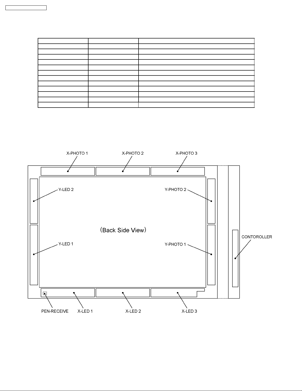
6 Printed Circuit Board Structure
6.1. TY-TP42P8-S
Board Name Board Number Function
CONTROLLER G441-K1TD11
PEN-RECEIVE G441-K1TD12 Touch Pen Remote Receiver
Y-LED 1 G441-K1TD07 IR Emitter to Y-PHOTO 1
Y-LED 2 G441-K1TD06 IR Emitter to Y-PHOTO 2
X-LED 1 G441-K1TD08 IR Emitter to X-PHOTO 1
X-LED 2 G441-K1TD09 IR Emitter to X-PHOTO 2
X-LED 3 G441-K1TD10 IR Emitter to X-PHOTO 3
Y-PHOTO 1 G441-K1TD01 IR Receiver from Y-LED 1
Y-PHOTO 2 G441-K1TD02 IR Receiver from Y-LED 2
X-PHOTO 1 G441-K1TD05 IR Receiver from X-LED 1
X-PHOTO 2 G441-K1TD04 IR Receiver from X-LED 2
X-PHOTO 3 G441-K1TD03 IR Receiver from X-LED 3
22
Page 23
6.2. TY-TP50P8-S
Board Name Board Number Function
CONTROLLER G541-K1TD13
PEN-RECEIVE G541-K1TD14 Touch Pen Remote Receiver
Y-LED 1 G541-K1TD08 IR Emitter to Y-PHOTO 1
Y-LED 2 G541-K1TD07 IR Emitter to Y-PHOTO 2
X-LED 1 G541-K1TD09 IR Emitter to X-PHOTO 1
X-LED 2 G541-K1TD10 IR Emitter to X-PHOTO 2
X-LED 3 G541-K1TD11 IR Emitter to X-PHOTO 3
X-LED 4 G541-K1TD12 IR Emitter to X-PHOTO 4
Y-PHOTO 1 G541-K1TD01 IR Receiver from Y-LED 1
Y-PHOTO 2 G541-K1TD02 IR Receiver from Y-LED 2
X-PHOTO 1 G541-K1TD06 IR Receiver from X-LED 1
X-PHOTO 2 G541-K1TD05 IR Receiver from X-LED 2
X-PHOTO 3 G541-K1TD04 IR Receiver from X-LED 3
X-PHOTO 4 G541-K1TD03 IR Receiver from X-LED 4
TY-TP42P8-S / TY-TP50P8-S
23
Page 24
TY-TP42P8-S / TY-TP50P8-S
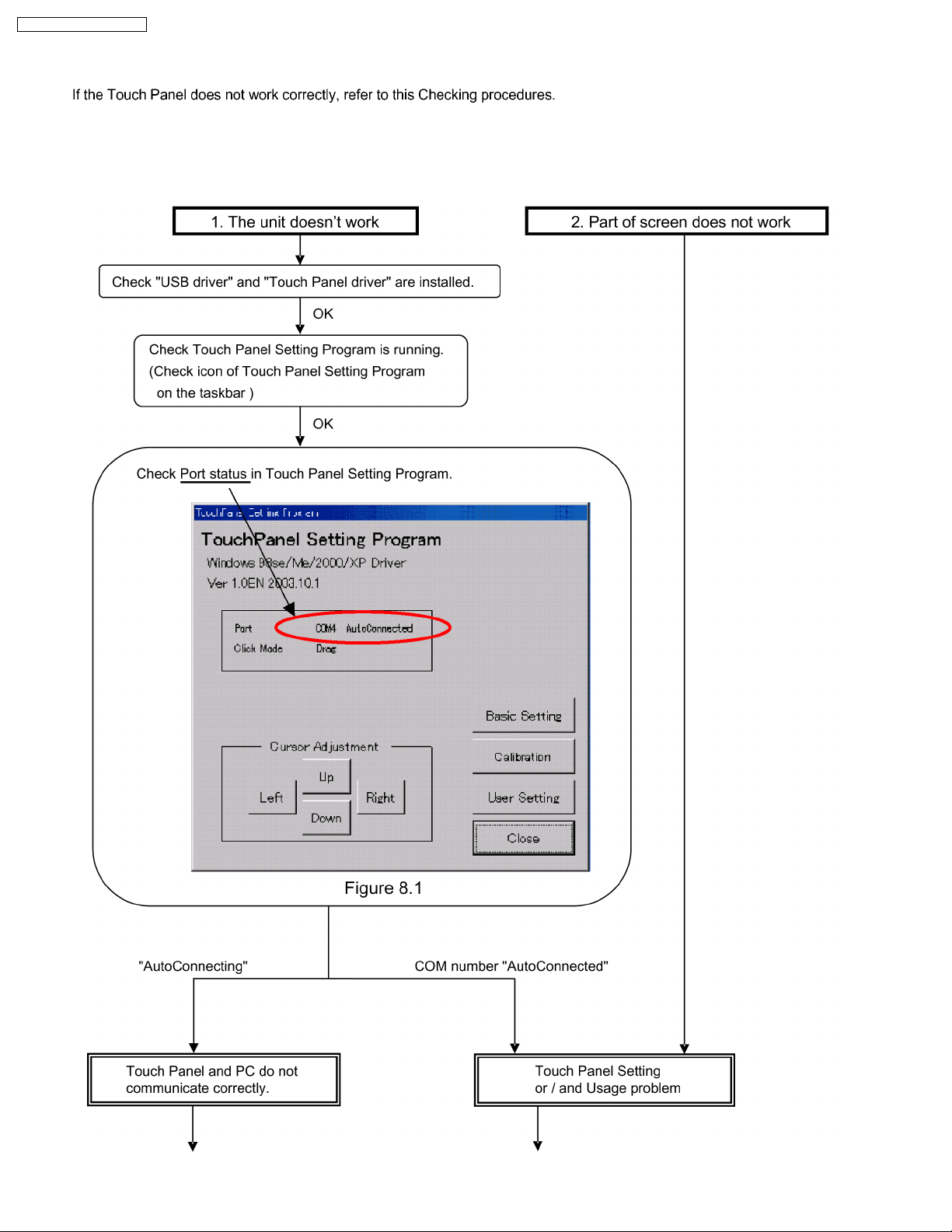
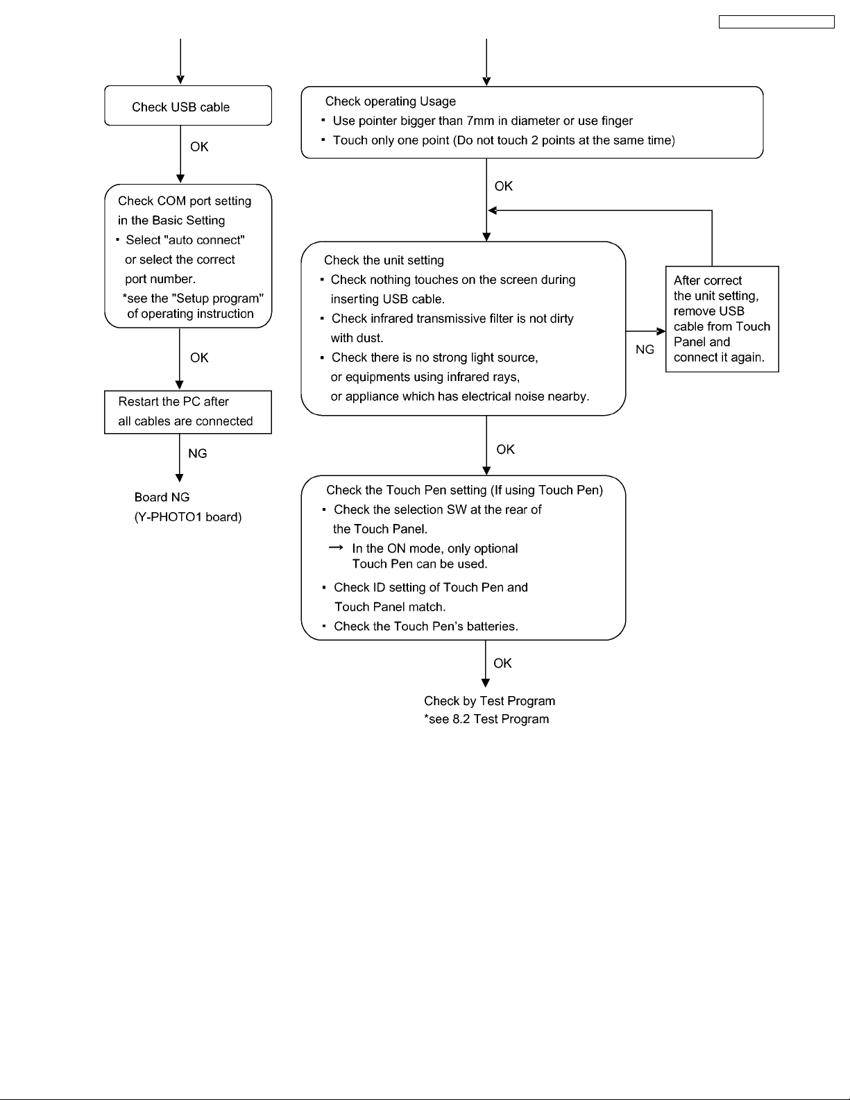
7 Trouble shooting
7.1. Checking procedures
24
Page 25
TY-TP42P8-S / TY-TP50P8-S
25
Page 26
TY-TP42P8-S / TY-TP50P8-S
7.2. Test Program
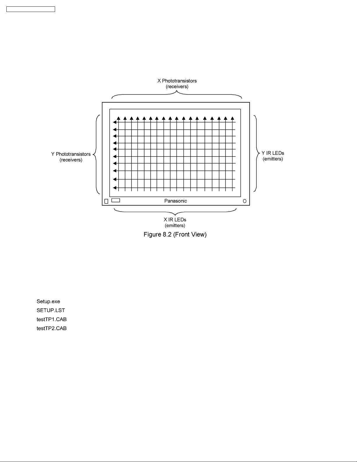
7.2.1. Function
Touch Panel Test Program is software to check operating status.
Touch Panel detects the location by cutting off the infrared ray from IR LEDs to phototransistors.
This program checks each line of infrared ray and finds out the location of defective IR LED and phototransistor.
7.2.2. Installation
There are 2 test programs. Program name “testTP42P8” is for TY-TP42P8-S, “testTP50P8” is for TY-TP50P8-S.
The installation program consists of following 4 files under one folder. The folder name is the same as test program, “testTP42P8”
or “testTP50P8”.
Run the ”Setup.exe” and follow the instructions. The test program “testTP50P8” or “testTP42P8” will be installed to your PC.
NOTES:
To Uninstall, delete “testTP50P8” or “testTP42P8” from the “Add/Remove Programs” of Control Panel.
26
Page 27
TY-TP42P8-S / TY-TP50P8-S
7.2.3. Set up
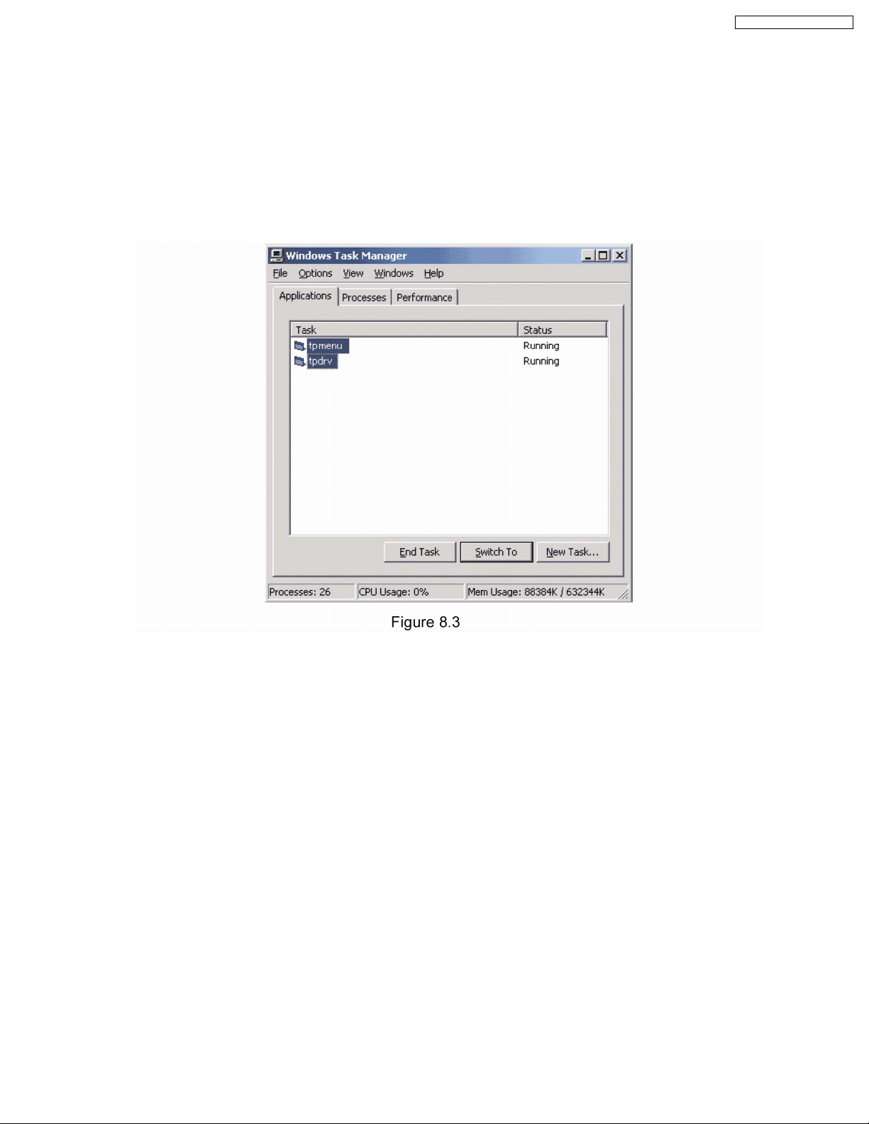
1. Check COM port number of Touch Panel from the menu of Touch Panel Setting Program(see Figure8.1. of Trouble Shooting)
or Device Manager of Windows(See the “Installation of the USB driver” of operating instruction).
The COM port number is necessary to set for this test program(see 8.2.4-2. COM port setting).
2. Change resolution of the PC monitor to higher than XGA(1024 x 768).
3. End the Touch Panel driver program by following procedure.
Press CTRL+ALT+DELETE to start Task Manager. Click the Applications tab, click the programs of “tpmenu” and “tpdrv”, and
then click End Task(This test program cannot be used while Touch Panel driver is running).
Below is the example of Windows XP.
27
Page 28
TY-TP42P8-S / TY-TP50P8-S
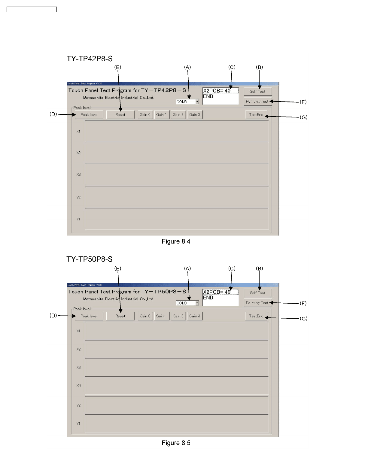
7.2.4. Operational Procedures
1. Start the Test Program
Click icon of “testTP42P8” or “testTP50P8” on start menu, then following window appears.
Below is an example window for “testTP42P8” or “testTP50P8”.
28
Page 29
2. COM port setting
Set the same COM port number of Touch panel(see 7.2.3.-1) into column (A).
3. Self Test
Self test is to check the operating condition of each IR LED and Phototransistor.
Click “Self Test” button (B) for initialization, and click (B) again. Then self test starts.
The result is shown in the textbox (C)
TY-TP42P8-S / TY-TP50P8-S
29
Page 30

TY-TP42P8-S / TY-TP50P8-S
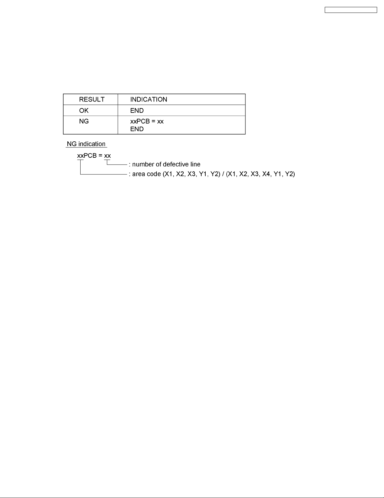
About the NG indication of the textbox C :
There are 6 areas of X1, X2, X3, Y1, and Y2. See Below “area location” for defective line. (TY-TP42P8-S)
There are 8 areas of X1, X2, X3, X4, Y1, and Y2. See Below “area location” for defective line. (TY-TP50P8-S)
30
Page 31

See Below “Location Number of defective line” for TY-TP42P8-S.
TY-TP42P8-S / TY-TP50P8-S
See Below “Location Number of defective line” for TY-TP50P8-S.
31
Page 32

TY-TP42P8-S / TY-TP50P8-S
For example, “X2PCB = 40” means 40th line of X2PCB area is defective.
NOTES:
· This program is to find out defective line. It cannot find out defective part, IR LED or phototransistor.
· If nothing appears in the textbox after clicking button(B) more than 2 times, check COM port or check if Touch Panel
driver programs is running(End the Program and restart Test Program).
· The definition of defective line is the received voltage from Phototransistor is less than 200mV.
32
Page 33

TY-TP42P8-S / TY-TP50P8-S
4. Peak level check
This is to see received level of all phototransistors.
Click “Peak Level” button(D). The received level is shown in the area of “X1”, “X2” and “X3” (TY-TP42P8),”X1”,”X2”, “X3”and
“X4” (TY-TP50P8) for vertical line, “Y1” and “Y2” for horizontal line. If the result of Self Test is NG, the received level of detected
defective line shows as lower than Red line.
Click “Reset” button(E) for ending the Peak level check.
NOTES:
The detection gain is automatically controlled while Touch Panel is operating and Self Test program is running.
33
Page 34

TY-TP42P8-S / TY-TP50P8-S
5. Pointing Test
Pointing test is to check the function of Touch Panel after repaired.
Click “Pointing Test” (F), then new window opens. The frame in window is the image of whole screen of Touch Panel.
Touch the Touch Panel then, the touched place is shown inside the frame.
Check the touch pen functions by touching the frame with the Touch Pen.
Check the Pen tip´s operation by "ON" / "OFF" shown in the Touch Pen status below.
Check the Function switch in the middle of the pen operating check by "ON" / "OFF" shown in the Touch Pen status below.
6. End
Click “TestEnd” button(G) to end the program.
After ending the test program, remove the USB cable and insert it again. Then, run the Touch Panel driver to use Touch Panel.
34
Page 35

8 Conductor Views
8.1. X-Photo1, X-Photo2, Y-Photo1 Board (42inch)
X-PHOTO1 / X-PHOTO2 / Y-PHOTO1 BOARD (COMPONENT SIDE)
G441-K1TD05 / G441-K1TD04 / G441-K1TD01
6
5
TY-TP42P8-S / TY-TP50P8-S
X-PHOTO1 / X-PHOTO2 / Y-PHOTO1 BOARD (FOIL SIDE)
G441-K1TD05 / G441-K1TD04 / G441-K1TD01
4
3
X-PHOTO1 X-PHOTO2
2
IC
U1
U2
U3
U4
U5
U6
U7
U8-U9
X-LED1 / X-LED2 / Y-LED1
TRANSISTOR
C-5
B-5
G-5
E-5
F-5
E-5
F-5
D-5
Q1 F-5
Y-PHOTO1
1
A
BCDEFGHI
35
Page 36

TY-TP42P8-S / TY-TP50P8-S
8.2. X-Photo1, X-Photo2, X-Photo3, Y-Photo1, Y-Photo2 Board (50inch)
X-PHOTO1 / X-PHOTO2 / X-PHOTO3 / Y-PHOTO1 / Y-PHOTO2 BOARD (COMPONENT SIDE)
G541-K1TD06 / G541-K1TD05 / G541-K1TD04 / G541-K1TD01 / G541-K1TD02
6
5
X-PHOTO1 / X-PHOTO2 / X-PHOTO3 / Y-PHOTO1 / Y-PHOTO2 BOARD (FOIL SIDE)
G541-K1TD06 / G541-K1TD05 / G541-K1TD04 / G541-K1TD01 / G541-K1TD02
4
3
X-PHOTO1 X-PHOTO2 X-PHOTO3
2
1
Y-PHOTO2
Y-PHOTO1
X-PHOTO1 / X-PHOTO2 / X-PHOTO3
Y-PHOTO1 / Y-PHOTO2
IC
U1
U2
U3
U4
U5
U6
U7
U8-U9
C-5
B-5
G-5
E-5
F-5
E-5
F-5
D-5
TRANSISTOR
Q1 F-5
A
BCDEFGHI
36
Page 37

8.3. X-Photo3 Board (42inch)
X-PHOTO3 BOARD (COMPONENT SIDE)
G441-K1TD03
6
5
TY-TP42P8-S / TY-TP50P8-S
X-PHOTO3 BOARD (FOIL SIDE)
G441-K1TD03
4
3
2
X-PHOTO3
IC
U1
U2
U3
U4
U5-U7
U6
U8-U9
X-PHOTO3
C-5
B-5
G-5
E-5
F-5
E-5
D-5
TRANSISTOR
Q1 F-5
1
A
BCDEFGHI
37
Page 38

TY-TP42P8-S / TY-TP50P8-S
8.4. X-Photo4 Board (50inch)
6
X-PHOTO4
X-PHOTO4 BOARD (COMPONENT SIDE)
G541-K1TD03
J17
J16
5
4
X-PHOTO4 BOARD (FOIL SIDE )
G541-K1TD03
X-PHOTO4
IC
U1
3
U2
U3-U6
U7-U8
D-5
E-5
D-5
C-5
TRANSISTOR
Q1 C-5
2
1
A
BCDEFGHI
38
Page 39

8.5. Y-Photo2 Board (42inch)
6
Y-PHOTO2 BOARD (COMPONENT SIDE)
G441-K1TD02
5
TY-TP42P8-S / TY-TP50P8-S
4
Y-PHOTO2 BOARD (FOIL SIDE)
G441-K1TD02
3
2
Y-PHOTO2
IC
U1-U2
U3
U4
U5
U6
U7
U8
Y-PHOTO2
B-5
D-5
C-5
D-5
C-5
D-5
C-5
TRANSISTOR
Q1 D-5
1
A
BCDEFGHI
39
Page 40

TY-TP42P8-S / TY-TP50P8-S
8.6. X-LED1, X-LED2, Y-LED1 Board (42inch)
X-LED1 / X-LED2 / Y-LED1 BOARD (COMPONENT SIDE)
G441-K1TD08 / G441-K1TD09 / G441-K1TD07
6
5
X-LED1 / X-LED2 / Y-LED1 BOARD (FOIL SIDE)
G441-K1TD08 / G441-K1TD09 / G441-K1TD07
4
3
2
X-PHOTO1 / X-PHOTO2 / Y-PHOTO1
IC
U1-U2
U3
U4-U5
U6
D-5
F-5
G-5
D-5
TRANSISTOR
Q1-Q9
Q10
Q11-Q16
Q17-Q18
D-5
E-5
G-5
H-5
Y-LED1
1
X-LED1 X-LED2
A
BCDEFGHI
40
Page 41

8.7. X-LED1, X-LED2, X-LED3, Y-LED1, Y-LED2 Board (50inch)
X-LED1 / X-LED2 / X-LED3 / Y-LED1 / Y-LED2 BOARD (COMPONENT SIDE)
6
G541-K1TD09 / G541-K1TD10 / G541-K1TD11 / G541-K1TD08 / G541-K1TD07
5
TY-TP42P8-S / TY-TP50P8-S
X-LED1 / X-LED2 / X-LED3 / Y-LED1 / Y-LED2 BOARD (FOIL SIDE)
G541-K1TD09 / G541-K1TD10 / G541-K1TD11 / G541-K1TD08 / G541-K1TD07
4
3
Y-LED2
2
Y-LED1
IC
U1-U2
U3
U4-U5
U6
X-LED1 / X-LED2 / X-LED3
Y-LED1 / Y-LED2
TRANSISTOR
D-5
F-5
G-5
D-5
Q1-Q9
Q10
Q11-Q16
Q17-Q18
D-5
E-5
G-5
H-5
1
X-LED1 X-LED2 X-LED3
ABCDEFGHI
41
Page 42

TY-TP42P8-S / TY-TP50P8-S
8.8. X-LED3 Board (42inch)
X-LED3 BOARD (COMPONENT SIDE)
G441-K1TD10
6
5
X-LED3 BOARD (FOIL SIDE)
G441-K1TD10
4
3
2
IC
U1-U2
U3
U4-U5
D-5
E-5
F-5
X-LED3
TRANSISTOR
Q1-Q5
Q6-Q10
Q11-Q18
C-5
D-5
F-5
1
X-LED3
A
BCDEFGHI
42
Page 43

8.9. X-LED4 Board (50inch)
TY-TP42P8-S / TY-TP50P8-S
6
X-LED4 BOARD (COMPONENT SIDE)
G541-K1TD12
5
4
X-LED4 BOARD (FOIL SIDE)
G541-K1TD12
X-LED4
X-LED4
IC
U1
3
U2-U3
U4
U5
C-5
D-5
E-5
C-5
TRANSISTOR
Q1-Q5
Q6-Q14
C-5
D-5
2
1
A
BCDEFGHI
43
Page 44

TY-TP42P8-S / TY-TP50P8-S
8.10. Y-LED2 Board (42inch)
Y-LED2 BOARD (COMPONENT SIDE)
G441-K1TD06
6
5
Y-LED2 BOARD (FOIL SIDE)
G441-K1TD06
4
3
2
Y-LED2
IC
U1
U2-U3
U4
U5
C-5
D-5
E-5
C-5
Y-LED2
TRANSISTOR
Q1-Q6
Q7
Q8-Q15
C-5
D-5
E-5
1
A
BCDEFGHI
44
Page 45

8.11. Controller Board (42inch)
CONTROLLER BOARD (COMPONENT SIDE)
G441-K1TD11
6
5
TY-TP42P8-S / TY-TP50P8-S
CONTROLLER BOARD (FOIL SIDE)
G441-K1TD11
4
3
2
CONTROLLER
IC
U1
U2
U3
U4
U5
U6
U7-U8
U9-U10
U11-U12
CONTROLLER
E-6
E-5
F-6
G-5
G-6
E-5
B-6
C-6
D-5
Q1
Q2
TRANSISTOR
E-5
C-5
1
A
BCDEFGHI
45
Page 46

TY-TP42P8-S / TY-TP50P8-S
8.12. Controller Board (50inch)
CONTROLLER BOARD (COMPONENT SIDE)
G541-K1TD13
6
5
CONTROLLER BOARD (FOIL SIDE )
G541-K1TD13
4
3
2
CONTROLLER
IC
U1
U2
U3
U4
U5
U6
U7-U8
U9-U10
U11-U12
CONTROLLER
TRANSISTOR
E-6
E-5
F-6
G-5
G-6
E-5
B-6
C-6
D-5
Q1
Q2
E-5
C-5
1
A
BCDEFGHI
46
Page 47

8.13. Pen-Receive Board (42inch)
PEN-RECEIVE BOARD (COMPONENT SIDE)
6
5
G441-K1TD12
TY-TP42P8-S / TY-TP50P8-S
PEN-RECEIVE BOARD (FOIL SIDE )
G441-K1TD12
PEN-RECEIVE
4
3
2
1
A
BCDEFGHI
47
Page 48

TY-TP42P8-S / TY-TP50P8-S
8.14. Pen-Receive Board (50inch)
6
5
PEN-RECEIVE BOARD (COMPONENT SIDE)
541-K1TD14
PEN-RECEIVE BOARD (FOIL SIDE )
G541-K1TD14
PEN-RECEIVE
4
3
2
1
A
BCDEFGHI
48
Page 49

9 Block Diagram
9.1. Overall Block Diagram (TY-TP42P8-S)
TY-TP42P8-S / TY-TP50P8-S
CONTROLLER
+5V
ALM LED
+5V
PEN MODE
SW
R-OUT
PENSW
PEN DATA
CONVERTER
J20
J21
J10
PEN DATA
SELECTION
RECEIVE from PHOTO
ADDRESS
YPHOTO-2
DECODER
(V)
ANALOG
SW
DECODER
(SEL)
YPHOTO-1
DECODER
(V)
PHOTO
Tr.
matrix
XPHOTO-3
J23 J11 J11
DECODER
(SEL)
ANALOG
PHOTO
Tr.
matrix
RECEIVER
IR RAY
RECEIVER
DECODER
(V)
J22
SW
DECODER
IR RAY
XPHOTO-2
(V)
DECODER
(SEL)
PHOTO
Tr.
matrix
IR RAY
ANALOG
SW
RECEIVER
J10
DECODER
(V)
XPHOTO-1
DECODER
(SEL)
PHOTO
Tr.
matrix
IR RAY
ANALOG
SW
RECEIVER
J10
EMITTER
YLED-2
IR
LED
matrix
YLED-1
PEN DATA
SELECTION
ADDRESS
DECODER
DECODER
DECODER
DECODER
DRIVER
(V)
(V)
DRIVER
(H)
(H)
(SEL)
DRIVER
(V)
(V)
J24
J25
J13
CPU
TXD/RXD
USB/RS232C
CONVERTER/
DRIVER
EEPROM
TY-TP42P8-S
Overall Block Diagram
RESET
+5V
POWER
FUSE
ANALOG
J9
J4
J11
SW
USB CONNECTOR
VBUS
D+
J1
D-
SW
DECODER
(SEL)
PHOTO IR
Tr.
matrix
RECEIVER
EMITTER
IR LED
matrix
IR RAY
EMITTER
IR LED
matrix
EMITTER
IR LED
matrix
matrix
EMITTER
PEN
RECEIVE
J27
DRIVER
(H)
DECODER
(H)
DECODER
(SEL)
XLED-3
(SEL)
DRIVER
(V)
(V)
J14
DRIVER
(H)
DECODER
(H)
DECODER
DRIVER
(V)
DECODER DECODER
(V)
J26
XLED-2
J14
DRIVER
(H)
DECODER
(H)
DECODER
XLED-1
(SEL)
DRIVER
(V)
DECODER
(V)
J15
J13J13
J1
LED
DECODER
DECODER
P1
PEN DATA
ADDRESS
SELECTION
DRIVER
(H)
(H)
(SEL)
TOUCH
PEN
IR RAY
TY-TP42P8-S
J14
Overall Block Diagram
49
Page 50

TY-TP42P8-S / TY-TP50P8-S
9.2. Overall Block Diagram (TY-TP50P8-S)
CONTROLLER
+5V
ALM LED
+5V
J10
J11
PEN DATA
SELECTION
RECEIVE from PHOTO
ADDRESS
YPHOTO-2
DECODER
(V)
ANALOG
SW
DECODER
(SEL)
PHOTO
Tr.
matrix
XPHOTO-1XPHOTO-2XPHOTO-3XPHOTO-4
J17 J16 J11 J11 J11J10 J10 J10
RECEIVER
DECODER
(V)
DECODER
(SEL)
ANALOG
SW
PHOTO
Tr. Tr.
matrix
RECEIVER RECEIVER RECEIVER RECEIVER
DECODER
(V)
DECODER
(SEL)
Tr.
matrix
ANALOG DECODER
SW
IR RAY
(V)
DECODER
(SEL)
PHOTO
matrix
ANALOG
SW
DECODER
(V)
DECODER
(SEL)
PHOTOPHOTO
Tr.
matrix
ANALOG
SW
EMITTER
YLED-2
IR
LED
matrix
PEN DATA
SELECTION
ADDRESS
DECODER
DECODER
DECODER
DRIVER
(V)
(V)
DRIVER
(H)
(H)
(SEL)
J13
J14
PEN MODE
SW
CPU
TXD/RXD
USB/RS232C
CONVERTER/
DRIVER
EEPROM
TY-TP50P8-S
Overall Block Diagram
R-OUT
PENSW
PEN DATA
CONVERTER
RESET
+5V
POWER
SW
FUSE
USB CONNECTOR
VBUS
D+
J1
D-
IR RAY IR RAY IR RAY IR RAY
J10
J9J4
J11
DECODER
(V)
ANALOG
SW
DECODER
(SEL)
YPHOTO-1
PHOTO
matrix
Tr.
RECEIVER
EMITTER EMITTER EMITTER EMITTER
IR LED
matrix
DECODER
(SEL)
DRIVER
(V)
DECODER
(V)(H)
DRIVER
(H) (V)
DECODER
J19
IR LED
matrix
(SEL)
DRIVER
DECODERDECODER
DRIVER
(H)
DECODER
(V)
J18
(H)
J14
IR RAY
J14
DRIVER
(H)
DECODER
(H)
IR LED
matrix
DECODER
(SEL)
DRIVER
(V)
DECODER
(V)
J14
DRIVER
(H)
DECODER
(H)
IR LED
matrix
DECODER
(SEL)
DRIVER
(V)
DECODER
(V)
EMITTER
J15 J1
J13J13J13
YLED-1
IR
LED
matrix
PEN
RECEIVE
DECODER
DECODER
DECODER
P1
PEN DATA
ADDRESS
SELECTION
DRIVER
(V)
(V)
DRIVER
(H)
(H)
(SEL)
TOUCH
IR RAY
PEN
J13
J14
XLED-4 XLED-3 XLED-2 XLED-1
TY-TP50P8-S
Overall Block Diagram
50
Page 51

9.3. Detail Block Diagram (1 of 3)
Signal explanations
Signal
AD0-6
SEL0-3
RANGE1-2
PHCOM1-4
LEDON
USB
CONNECTOR
Function
Address signals to switch LEDs and photo-transistors
Selection signals for the LED and photo-transistor boards.(active LOW)
Selection for 3 to 8 line decoder.
3 TO 8 LINE DECODER(X-PHOTO:U1,X-LED:U3)
G2A C B A
LL
LL
LH
L
L
HHHL
L
L
L
L
Y0 Y1 Y2 Y3
L
L
Selection board Selection board
X-PHOTO 2 & X-LED 2
L
X-PHOTO 3 & X-LED 3
L
X-PHOTO 4 & X-LED 4
Signals to change photo-transistor gain.
Photo-transistor output signal(analog voltage) output
from each photo-transistor board.
Signals to light IR-LED.(active LOW)
Signals to activate photo-transistor.(active LOW)PHON
CONTROLLER BOARD
FUSE2
U10
J1
FUSE1
1
VBUS
2
D-
3
D+
U7
EEPROM
U1
RESET
RESET
RESET
U6
+5V
SH2 SH1
Y1 Y
ANALOG
MULTI-
A
PLEXER
B
C
+5V
X
Y1 PWE
Z MD2
Z1
XTAL
+5V
20MHz
+
ALARM
LED
SW1
PEN
MODE
SW
VIN2
VIN1
U8
USBDM
USBSP
3 TO 8 LINE DECODER(Y-PHOTO:U2,Y-LED:U4)
G2A
OUT1
POWER
CONTROL / SW
OUT2
PWREN
EN1
EN2
USB DRIVER
TXD RXD
U3
RXD1 TXD1 TXD0 RXD0
RES
CPU
XTAL
EXTAL
Vref
ALM
PENMODE
ALLB
CY0
L
LL
LX-PHOTO 1 & X-LED 1
LH
+5V
L
L
U9
1Y
Q2
XTAL2
6MHz
AD0
AD6
SEL0
SEL3
LEDON
PHON
RANGE1
RANGE2
PENDATA
PHCOM
ILEDCOM
ROUT1
ROUT2
PENSW1
PENSW2
Y1
Y-PHOTO 1 & Y-LED 1
Y-PHOTO 2 & Y-LED 2
1B
NOR GATE
POWER SELECT
1A
U11
U12
DAT/GP0
CLK/GP1
GP4
GP5
RS232C
DRIVER
U4
BUFFER
BUFFER
PEN DATA
CONVERTER
TY-TP42P8-S / TY-TP50P8-S
TO
X-PHOTO 3 BOARD
(J23:42inch)
J20
(42inch)
TO
J10
X-PHOTO 4 BOARD
Y-PHOTO 2 BOARD
PHOUT SW
U5
PH ON,RANGE1,2
A B C
U6
OPTICAL NOISE CANCEL
+5V
J21
(42inch)
J11
(50inch)
AD0
119
J10
9151481
7
AD6
PHON
7
RANGE1
RANGE2
9
LEDON
13
10
16
20 1821
17 19
+5V
+5V
PHCOM
ILEDCOM
17
+5V
18821
SEL0
SEL3
PENDATA
20
13101514
16
PHCOM
CH0
INHCOM
SELCOM
U7
Q1
XY
ZZ1
GAIN CONTROL
SEL0-3
U2U3
3 TO 8
LINE
DECODER
Y1
U4
A B C
8ch
ANALOG
MULTI-
INH
PLEXER
COM
PH.SINK1-8
PHOTO-TRANSISTOR
MATRIX
P1-P52
(42inch)
P1-P78
(50inch)
AD0-2 AD3-6
3 TO 8
LINE
DECODER
U8,U9
(U9:50inch
ONLY)
PH.DRV1-7
(42inch)
PH.DRV1-10
(50inch)
(50inch)
(J17:50inch)
1
AD0
7
AD6
PHON
8
14
RANGE1
15
RANGE2
9
LEDON
10
SEL0
13
SEL3
16
PENDATA
20
PHCOM
21
ILEDCOM
17
+5V
+5V
18
+5V
19
+5V
Y-PHOTO 1
SEL0-3
A B C
PH.SINK1-8
BOARD
AD0-2 AD3-6
3 TO 8
LINE
DECODER
PH.DRV1-10
U8,U9
+5V
NO
J11
USE
17
+5V
18
+5V
19
+5V
21
ILEDCOM
20
PHCOM
16
PENDATA
10
SEL0
13
SEL3
9
LEDON
8
PHON
14
RANGE1
15
RANGE2
1
AD0
7
AD6
U2U3
PHCOM
CH0
PHOUT SW
COM
INH
SELCOM
3 TO 8
LINE
DECODER
Y1
U4
J4
1
7
U5
INT
GP2
10
13
9
8
14
15
16
20
21
+5V
17
18
19
AD0
AD6
SEL0
SEL3
LEDON
PHON
RANGE1
RANGE2
PENDATA
PHCOM
ILEDCOM
+5V
+5V
+5V
J9
1
7
10
13
9
8
14
15
16
20
21
17
+5V
18
19
U5
PH ON,RANGE1,2
U6
ZZ1
A B C
OPTICAL NOISE CANCEL
GAIN CONTROL
U7
INH
COM
ANALOG
MULTIPLEXER
MATRIX
8ch
Q1
X
Y
PHOTO-TRANSISTOR
P1-P78
TY-TP42/50P8-S
Detail Block Diagram (1 of 3)
TY-TP42/50P8-S
Detail Block Diagram (1 of 3)
51
Page 52

TY-TP42P8-S / TY-TP50P8-S
9.4. Detail Block Diagram (2 of 3)
J16
1
7
8
14
15
9
10
13
16
20
21
17
18
19
TO
Y-PHOTO 2 BOARD
(J20:42inch)
J23
(42inch)
J11
(50inch)
AD0
AD6
PHON
RANGE1
RANGE2
LEDON
SEL0
SEL3
PENDATA
PHCOM
+5V
+5V
+5V
J22
(42inch)
1
X-PHOTO 3 BOARD
7
8
14
15
9
10
13
16
20
21
17
18
19
U1
Y2
3 TO 8
LINE
DECODER
U3
CH0
PHOUT SW
SELCOM
INH
U5
COM
AD3-6
AD0-2
U8,U9
3 TO 8
LINE
DECORDER
U4
A
8ch
B
ANALOG
C
MULTIPLEXER
INH
COM
PH.DRV1-10
PH.SINK1-8
U6
A
B
OPTICAL
C
NOISE
CANCEL
X
GAIN
CONTROL
Y
Z
Q1
Z1
PHOTOTRANSISTOR
MATRIX
P1-P75(42inch)
P1-P78(50inch)
+5V
J10
(50inch)
14
15
10
13
16
20
21
17
18
19
1
7
8
9
AD0
AD6
PHON
RANGE1
RANGE2
LEDON
SEL0
SEL3
PENDATA
PHCOM
+5V
+5V
+5V
U7
TO
Y-PHOTO 2 BOARD
(J10:50inch)
J17
1
AD0
7
AD6
PHON
8
14
RANGE1
15
RANGE2
9
LEDON
10
SEL0
13
SEL3
16
PENDATA
20
PHCOM
21
ILEDCOM ILEDCOM ILEDCOM
17
+5V
18
+5V
19
+5V
U1
3 TO 8
LINE
SEL0-3 SEL0-3 SEL0-3
DECODER
U3
CH0
PHOUT SW
X-PHOTO 4 BOARD
U8
AD3-6
Y3
AD0-2
SELCOM
INH
COM
U5
3 TO 8
LINE
DECODER
U4
8ch
A
ANALOG
B
MULTI-
C
PLEXER
INH
COM
PH ON,RANGE1,2 PH ON,RANGE1,2 PH ON,RANGE1,2
PH.SINK1-8
Q1
PH.DRV1-6
U6
A
B
C
X
Y
Z
Z1
50inch only
PHOTOTRANSISTOR
MATRIX
P1-P43
OPTICAL
NOISE
CANCEL
GAIN
CONTROL
+5V
U7
TO
X-PHOTO 1 BOARD
(J11)
J11
1
7
8
14
15
9
10
13
16
20
21
17
18
19
U1
3 TO 8
LINE
DECORDER
U3
CH0
X-PHOTO 2 BOARD
AD3-6
Y1
AD0-2
SELCOM
INH
PHOUT SW
COM
U5
U8,U9
3 TO 8
LINE
DECORDER
U4
8ch
A
B
ANALOG
C
MULTIPLEXER
INH
COM
+5V
PH.DRV1-10
PHOTOTRANSISTOR
MATRIX
PH.SINK1-8
P1-P78
U6
A
B
OPTICAL
C
NOISE
CANCEL
X
GAIN
Y
CONTROL
Z
Q1
Z1
J10
1
AD0
7
AD6
PHON
8
14
RANGE1
15
RANGE2
9
LEDON
10
SEL0
13
SEL3
16
PENDATA
20
PHCOM
21
ILEDCOM
17
+5V
18
+5V
19
+5V
U7
X-LED 4 BOARD
U1
U5
A
B
C
G2A
G2B
3 TO 8
LINE
DECODER
3 TO 8
LINE
DECODER
L.SINK1-8
AD3-6
U3
3 TO 8
LINE
DECODER
U6
NO
USE
J19
1
AD0
7
AD6
10
SEL0 SEL0
13
SEL3
9
LEDON
21
ILEDCOM
17
+5V
18
+5V
19
+5V
AD0-2
Y3
SELCOM
INHCH0
+5V
COM
Q1-Q6
LED
DRIVE
Q7-Q14
LED
SINK
L.DRV1-6
LED
MATRIX
L1-L43
+5V
X-LED 3 BOARD
U1,U2
U5
A
B
C
G2A
G2B
3 TO 8
LINE
DECODER
3 TO 8
LINE
DECODER
L.SINK1-8
AD3-6
U3
3 TO 8
LINE
DECODER
U6
ILEDOUT SWILEDOUT SW
J27
(42inch)
J18
10
13
21
17
18
19
J14
(50inch)
1
7
9
AD0
AD6
SEL3
LEDON
ILEDCOM
ILEDCOM
+5V
+5V
+5V
1
7
10
13
9
21
17
18
19
AD0-2
Y2
SELCOM
INHCH0
+5V
COM
Q1-Q10
LED
DRIVE
Q11-Q18
LED
SINK
L.DRV1-10
LED
MATRIX
L1-L75
(42inch)
L1-L78
(50inch)
U3
3 TO 8
SEL0-3SEL0-3SEL0-3
LINE
DECODER
U6
CH0
ILEDOUT SW
J26
(42inch)
J13
(50inch)
1
7
10
13
9
21
+5V
17
18
19
AD0
AD6
SEL0
SEL3
LEDON
ILEDCOM
+5V
+5V
+5V
J14
1
7
10
13
9
21
17
18
19
X-LED 2 BOARD
U1,U2
AD3-6
AD0-2
Y1
SELCOM
INH
+5V
COM
3 TO 8
LINE
DECODER
U5
A
B
3 TO 8
C
LINE
DECODER
G2A
G2B
L.SINK1-8
Q1-Q10
LED
DRIVE
Q11-Q18
LED
SINK
L.DRV1-10
LED
MATRIX
L1-L78
TO
X-LED 1
BOARD
(J14)
J13
1
AD0
7
AD6
10
SEL0
13
SEL3
9
LEDON
21
+5V
ILEDCOM
17
+5V
18
+5V
19
+5V
TY-TP42/50P8-S
Detail Block Diagram (2 of 3)
TY-TP42/50P8-S
Detail Block Diagram (2 of 3)
52
Page 53

9.5. Detail Block Diagram (3 of 3)
TO
X-PHOTO 2 BOARD
(J10)
J11
1
AD0
7
AD6
PHON
8
14
RANGE1
15
RANGE2
9
LEDON
10
SEL0
13 13
SEL3
16
PENDATA
20
PHCOM
21
ILEDCOM
17
+5V
18
+5V
19
+5V
U1
3 TO 8
LINE
DECORDER
SEL0-3
U3
CH0
PHOUT SW
X-PHOTO 1 BOARD
U8,U9
AD3-6
3 TO 8
LINE
DECORDER
Y0
U4
A
AD0-2
SELCOM
INH
U5
COM
8ch
B
ANALOG
C
MULTIPLEXER
INH
COM
PH ON,RANGE1,2
Q1
X-LED 1 BOARD
U1,U2
AD3-6
3 TO 8
LINE
DECODER
U7
PH.SINK1-8
Q1-Q10
PH.DRV1-10
U6
A
B
C
X
Y
Z
Z1
LED
DRIVE
PHOTOTRANSISTOR
MATRIX
P1-P78
OPTICAL
NOISE
CANCEL
GAIN
CONTROL
L.DRV1-10
TY-TP42P8-S / TY-TP50P8-S
J24
(42inch)
AD0
AD6
PHON
RANGE1
RANGE2
LEDON
SEL0
SEL3
PENDATA
PHCOM
ILEDCOM
+5V
+5V
+5V
J13
(50inch)
10
13
16
21
17
18
19
1
7
9
U2,U3
(42inch)
U3,U4
(50inch)
Y1
3 TO 8
LINE
DECODER
SELCOM
CH0
INH
ILEDOUT SW
COM
Y-LED 2 BOARD
3 TO 8
LINE
DECORDER
A
B
3 TO 8
C
LINE
DECODER
G2A
G2B
(U2:50inch
ONLY)
U1,U2
AD3-6
U4(42inch)
U5(50inch)
AD0-2
U5(42inch)
+5V
U6(50inch)
L.SINK
1-8
Q1-Q7(42inch)
Q1-Q10(50inch)
LED
DRIVE
TRAN-
SISTORS
Q8-Q15(42inch)
Q11-Q18(50inch)
LED
TRANSISTORS
L.DRV1-7(42inch)
L.DRV1-10(50inch)
LED
MATRIX
L1-L52(42inch)
L1-L78(50inch)
J25
(42inch)
J14
(50inch)
J13
1191679
AD0
AD6
10
LEDON
13 17
SEL0
13
SEL3
+5V
21
18
+5V
+5V
+5V
ILEDCOM
PENDATA
17710
1921 189161
J10
1
7
8
14
15
9
10
16
20
21
17
+5V
18
19
Y-LED 1 BOARD
+5V
AD3-6
U1,U2
3 TO 8
LINE
DECODER
Q1-Q10
LED
DRIVE
L.DRV1-10
TO
X-LED 2 BOARD
(J13)
ILEDCOM
TY-TP42/50P8-S
Detail Block Diagram (3 of 3)
SEL0
SEL3
LEDON
L.SINK1-8
J1
1
2
Q11-Q18
LED
SINK
P1
PEN IR
RECEIVER
PHOTO
TRANSISTORS
LED
MATRIX
L1-L78
PENRECEIVER
BOARD
U4
3 TO 8
SEL0-3SEL0-3
LINE
DECODER
Y0
U6
TOUCH
PEN
IR RAY
J13
1
7
10
13
9
16
21
+5V
17
18
19
AD0
AD6
SEL0
SEL3
LEDON
PENDATA
ILEDCOM
+5V
+5V
+5V
J14
1
7
10
13
9
16
21
17
18
19
INHCH0
ILEDOUT SW
COM
AD0-2
SELCOM
+5V
A
B
C
G2A
G2B
U5
3 TO 8
LINE
DECODER
L.SINK1-8
Q11-Q18
LED
SINK
LED
MATRIX
L1-L78
U3
3 TO 8
LINE
DECODER
U6
CH0
INH
ILEDOUT SW
COM
J14
1
AD0
7
AD6
10
13
9
21
17
+5V
18
+5V
19
+5V
AD0-2
SELCOM
+5V
A
B
3 TO 8
C
LINE
DECODER
G2AY0
G2B
U5
+5V
J15
1
+5V
2
PENDATA
TY-TP42/50P8-S
Detail Block Diagram (3 of 3)
53
Page 54

TY-TP42P8-S / TY-TP50P8-S
54
Page 55

10 Schematic Diagram
10.1. Controller Board Schematic Diagram
TY-TP42P8-S / TY-TP50P8-S
GND
8
+5V
VDD
+5V
VCC
GND
10
+5V
VCC
GND
10
1
GP2/INT
R67
R68
+5V
C31
0.1u
C36
0.1u
2
VCC16V+
11
T1
12
R1
10
T2
9
R2
1
C1+
3
C1-
4
C2+
5
C2-
GND
16
C13
0.1u
20
18
Y1
17
Y2
16
Y3
15
Y4
14
Y5
13
Y6
12
Y7
PWEA
11
Y8
C14
0.1u
20
RANGE1
18
Y1
RANGE2
17
LEDON
16
Y3
PHON
15
Y4
SEL0
14
Y5
SEL1
13
Y6
SEL2
12
Y7
SEL3
11
Y8
U5
74HC54
BUFFER
C36
0.1u
4
VPPGP0/DAT
5
+5V
150
0
R65
14
R66
13
7
8
6
V-
C35
0.22u
AD0
AD1
AD2
AD3
AD4
AD5
AD6
AD0
AD1
AD2
AD3
AD4
AD5
AD6
PHON
LEDON
SEL0
SEL1
SEL2
SEL3
RANGE1
RANGE2
PENDATA
PHCOM
ILEDCOM
FC1
200
FC2
200
TO
YPHOTO-1 BOARD
(J9)
J4
1
AD0
2
AD1
3
AD2
4
AD3
5
AD4
6
AD5
7
AD6
8
PHON
9
LEDON
10
SEL0
11
SEL1
12
SEL2
13
SEL3
14
RANGE1
15
RANGE2
16
PENDATA
5V
17
+5V
18
+5V
19
+5V
20
PHCOM
21
ILEDCOM
22
GND
23
GND
24
GND
25
NC
26
NC
CONTROLLER BOARD
G441-K1TD11 (TY-TP42P8-S)
G541-K1TD13 (TY-TP50P8-S)
A
C6
+5V
D1
1S2835
10k
C3
0.33u
31
2
U1
MB3773
RESET
31
2
D2
1S2835
+5V
C5
0.1u
1
VCC
1
CT
2
RESET
3
CK
8
RESET
7
VS
6
VREF
GND
4
C4
0.1u
+5V
R3
R2
3.3k
1k
R4
1.5k
HD64F3067
XTAL1
20MHz
U3
CPU
63
67
1
2
66
3
0.33u
R1
C2
B
5V
C15
FUSE1
USB CONNECTOR
1.00A
J1
VBUS
1
D-32
D+
GND
4
D4
NNCD6.2MF NNCD6.2MF
C
D
E
31
13
2
D7
NNCD6.2MF
+5VUSB
C16
0.1u
31
D5
C20
0.1u
6
7
2
NC
NC
FUSE2
1.00A
+
C17
16V
2.2u
31
2
8
VCC
DOUT
GND
5
BR93L46RF-W
EEPROM
NOR GATE
POWER SELECT
+5VIN
D6
NNCD6.2MF
DIN
CS
SK
U7
U9
TC7W02
C25
0.1u
2
+5VUSB
4
3
1
2
R48
R49
XTAL2
6MHz
R52
10k
R53
2.2k
1
1A
2
1B
3
2Y 2A
FT232BL
USB DRIVER
27
27
1
2
3
C21
0.033u
+5VUSB
VCC
GND
U8
1.5k
8
4
+5VUSB
3
VCC26VCC
8
USBDM
USBP
RSTOUT
XIN
XOUT
3V3OUT
AGND
TEST
EEDATA
EECS
EESK
GND17GND
9
RESET
VCC-IC
TZDEN
PWREN
PWRCTL
TXLED
RXLED
SLEEP
7
R50
5
27
28
6
29
31
2
32
1
AVCC
C22
0.1u
4
13
25
TXD
24
RXD
23
RTS
22
CTS
21
DTR
20
DSR
19
DCD
18
RI
16
15
14
12
11
10
30
+5VUSB
+5VIN
R57
470
C23
0.1u
U10
MB3842
RXD1
TXD1
U6
74HC4053
ANALOG
MULTIPLEXER
R54
100k
R56
0
11
10
R47
9
10k
6
12
2
5
POWER CONTROL/SW
C24
0.1u
7
1Y
6
2B
R58
5
100k
Q2
FB1L2Q
+5VUSB
4
VIN1
5
VIN1
1
EN1
C26
0.01u
2
SS1
R59
R60
C27
R61
10k
3
2k
CS1
8
2k
CS2
0.01u
9
SS2
6
VIN2
7
VIN2
10
EN2
C28
R62
100k
0.1u
OUT1
OUT1
OUT1
OUT2
OUT2
OUT2
18
17
16
15
14
13
19
OC1
12
OC2
20
GND
11
GND
+5V
C30
+
C29
6.3V
0.1u
47u
+5VUSB
R63
R64
+5VIN
100k
100k
0.1u
16
VCC
A
B
C
INH
X0
Y0
Z0
VSS
VEE
PHCOM
ILEDCOM
+5V
5V
X
14
X1
13
15
Y
1
Y1
4
Z
3
Z1
78
1k
R6
1k
R7
C8
C9
3300p
470p
R10
R11
C10
+
C11
6.3V
47u
0.1u
C12
0.1u
31
D3
1S2835
R13
100
5V
R15
10k
87
88
89
90
91
93
94
95
96
97
98
99
100
2
3
4
5
6
7
8
9
58
59
60
69
70
71
72
61
78
79
R8
0
80
R9
0
81
82
83
0
84
0
85
1
+5V
R14
10k
2
6.3V
47u
+
C7
0.1u
35 68
VCCVCC
RES
XTAL
STBY
EXTAL
P90/TXD0
P91/TXD1
P92/RXD0
P93/RXD1
P80
P81
P82
P83
P84
PA0
PA1
PA2
PA3
PA4
PA5
PA6
PA7
PB0
PB1
PB2
PB3
PB4
PB5
PB6/TXD2
PB7/RXD2
P60
P61
P62
P63
P64
P65
P66
P67
P60
P61
P62
P63
P64
P65
P66
P67
VCC
76
AVCC
77
VREF
86
AVSS
10
PWE
5V 5V
R16-20
73
MD0
74
MD1
75
MD2
62
64
NMI
12
13
14
15
16
P94
17
P95
36
P10
37
P11
38
P12
39
P13
40
P14
41
P15
42
P16
43
P17
45
P20
R30
46
P21
510
47
P22
48
P23
49
P24
50
P25
51
P26
52
P27
27
P30
28
P31
29
P32
30
P33
31
P34
32
P35
33
P36
34
P37
53
P50
54
P51
55
P52
56
P53
18
P40
19
P41
20
P42
21
P43
23
P44
24
P45
25
P46
26
P47
11
VSS
22
VSS
44
VSS
57
VSS
65
VSS
72
VSS
10k
ALM LED
5V
R28,29
10k
R25-27
10k
R21-24
10k
+5V
TY-TP42/50P8-S
Controller Board Schematic Diagram
TXD0
TXD1
RXD0
RXD1
1
2
3
4
5
6
7
8
9
10
11
12
13
14
15
16
PENMODE
PENSW1
PENSW2
R-OUT1
R-OUT2
TXD0
RXD0
31
D8
NNCD12F
1
2
3
4
5
6
7
16
8
9
10
11
12
13
14
15
R-OUT1
R-OUT2
PENSW1
PENSW2
PENMODE
2
U12
PIC12F629
PEN DATA
CONVERTER
6
4
2
U11
MAX202CSE
RS232C DRIVER
1
3
2
R38
10k
D9
NNCD12F
5V
R31-37
10k
U4
74HC54
C33
0.22u
C34
0.22u
1
G1
19
G2
2
A1
3
A2
4
A3
5
A4
6
A5
7
A6
8
A7
9
A8
BUFFER
5V
R39-46
10k
1
G1
19
G2
2
A1
3
A2 Y2
4
A3
5
A4
6
A5
7
A6
8
A7
9
A8
7
6
GP1/CLK
3
GP4
2
GP5
SW1
PEN MODE SW
5
1
3
TY-TP42/50P8-S
Controller Board Schematic Diagram
3
42 7
56
81
55
Page 56

TY-TP42P8-S / TY-TP50P8-S
10.2. X-Photo 1 Board Schematic Diagram
5V
5V
5V
A
SEL0
SEL1
SEL2
SEL3
R17-20
10k
5V
B
C
PHCOM
5V
C1
0.1u
16
1
A
2
B
3
C
6
G1
4
G2A
5
G2B
1
A
2
B
3
C
6
G1
49
G2A
5
G2B
CH0
CH1
VEE
15
COM
R1
Y0
14
Y1
13
Y2
12
Y3
11
Y4
10
Y5
9
Y6
7
Y7
U1
74HC138
3 TO 8 LINE
DECODER
C2
0.1u
15
Y0
14
Y1
13
Y2
12
Y3
11
Y4
10
Y5
Y6
7
Y7
U2
74HC138
3 TO 8 LINE
DECODER
C3
0.1u
17
26
INH
5
A
4
U3
TC7W53FK
VCC
GND
8
5V
16
VCC
GND
8
5V
8
VCC
GND
3
AD0
AD1
AD2
0
R21-24
10k
U5
UPC842G
R30
2k
PHOUT SW
TO Y-LED 2 BOARD(J13)(TY-TP50P8)
TO Y-LED 2 BOARD(J24)(TY-TP42P8)
AD0
1
AD1
2
AD2
3
AD3
D
E
C23
6.3V
47u
4
AD4
5
AD5
6
AD6
7
PHON
8
SEL0
10
SEL1
11
SEL2
12
SEL3
13
RANGE1
14
RANGE2
15
5V 5V
PHCOM
17 17
5V
+
C22
0.1u
TY-TP42/50P8-S
J10 J11
1
1
2
3
4
5
6
7
8
9
10
11
12
13
14
15
16
17
18
AD0
2
AD1
3
AD2
4
AD3
AD4
5
6
AD5
7
AD6
PHON
8
9
LEDON
10
SEL0
SEL1
11
SEL2
12
13
SEL3
RANGE1
14
15
RANGE2
16
PENDATA
17
+5V
18
+5V
19
+5V
20
PHCOM
21
ILEDCOM
22
GND
GND
23
GND
24
NC
25
NC
26
TO
X-PHOTO 2 BOARD
(J10)
1
2
3
4
5
6
7
8
9
10
10
11
11
12
12
13
13
14
14
15
15
16
16
17
18
19
20
18
21
22
23
24
25
26
1
2
3
4
5
6
7
8
9
11
10
9
6
3
A
B
C
INH
COM
R28
100k
7
R31
100k
AD0
AD1
AD2
AD3
AD4
AD5
AD6
PHON
LEDON
SEL0
SEL1
SEL2
SEL3
RANGE1
RANGE2
PENDATA
+5V
+5V
+5V
PHCOM
ILEDCOM
GND
GND
GND
NC
NC
5V
C4
0.1u
16
13
VCC
0
14
1
15
2
12
3
1
4
5
5
2
6
4
7
VEE
VSS
7
8
74HC4051
8ch
ANALOG
MULTIPLEXER
R29
10k
5
+
6
R32
10k
U4
U5
UPC842G
PH.SINK1
PH.SINK2
PH.SINK3
PH.SINK4
PH.SINK5
PH.SINK6
PH.SINK7
PH.SINK8
5V
C5
0.1u
2
8
-
1
3
+
R33
4
2k
AD3
AD4
AD5
AD6
RANGE1
RANGE2
PHON
C6
3300p
Q1
FB1L2Q
R37
200
R38
5V
2k
1
UPC842G
5V
8
4
U7
7
R25-27
10k
-
+
R39-42
C8
0.1u
2
3
U7
UPC842G
+
-
10k
5V
11
10
9
6
14
15
4
5
6
X-Photo 1 Board Schematic Diagram
5V
C10
0.1u
16
1
A
2
B
3
C
6
G1
4
G2A
5
G2B
1
A
2
B
3
C
6
G1
49
G2A
5
G2B
5V
16
VCC
A
B
C
INH
X
Y
Z
VEE
VSS
8
OPTICAL NOISE CANCEL,
GAIN CONTROL
C9
3300p
15
VCC
Y0
14
Y1
13
Y2
12
Y3
11
Y4
10
Y5
9
Y6
7
Y7
GND
8
5V
C11
0.1u
16
VCC
GND
8
C7
0.1u
12
X0
13
X1
2
Y0
1
Y1
5
Z0
3
Z1
7
15
Y0
14
Y1
13
Y2
12
Y3
11
Y4
10
Y5
Y6
7
Y7
U6
74HC4053
U8
74HC238
3 TO 8 LINE
DECODER
R34
2k
R35
5.1k
R36
1.2k
PH.DRV1
PH.DRV2
PH.DRV3
PH.DRV4
PH.DRV5
PH.DRV6
PH.DRV7
PH.DRV8
PH.DRV9
PH.DRV10
U9
74HC238
3 TO 8 LINE
DECODER
PH.DRV5
PH.DRV4
PH.DRV3
PH.DRV2
PH.DRV1
P25P1
PH.SINK1
PH.SINK2
PH.SINK3
PH.SINK4
PH.SINK5
PH.SINK6
PH.SINK7
PH.SINK8
P2 P50
P3
P4
P5
P6
P7
P8
P17P9
P10
P11
P12
P13
P14
P15 P31
P16
C12
0.1u
P26
C14
0.1u
C
P27
P29
P30
P32
P1-P78
PT100MF0MP
P34
P35
P36
P37
P38
P39
P40
C15
0.1u
P18 P74
P19
P20
P21
P22
P23
P24
C13
0.1u
PHOTO
TRANSISTOR
MATRIX
E
X-PHOTO 1 BOARD
G441-K1TD05 (TY-TP42P8-S)
G541-K1TD06 (TY-TP50P8-S)
TY-TP42/50P8-S
X-Photo 1 Board Schematic Diagram
PH.DRV6
P49
P41
P42
P43
P44P28
P52
P45
P53
P46
P54
P55
P47
P56
P48
C16
C17
0.1u
0.1u
P65P33
P57
P66
P58
P59
P67
P68
P60
P61
P69
P70
P62
P71
P63
P64
P72
C18
C19
0.1u
0.1u
PH.DRV10
R43
P73
10k
R44
10k
R45
10k
P75P51
R46
10k
P76
R47
P77
10k
R48
10k
P78
R49
10k
R50
10k
C20
C21
0.1u
0.1u
PH.DRV9
PH.DRV8
PH.DRV7
3
42 7
56
81
56
Page 57

10.3. X-Photo 2 Board Schematic Diagram
TY-TP42P8-S / TY-TP50P8-S
5V
5V
5V
A
SEL0
SEL1
SEL2
SEL3
R17-20
10k
5V
B
C
PHCOM
5V
C1
0.1u
16
1
A
2
B
3
C
6
G1
4
G2A
5
G2B
1
A
2
B
3
C
6
G1
49
G2A
5
G2B
CH0
CH1
VEE
15
VCC
Y0
14
R2
Y1
13
Y2
12
Y3
11
Y4
10
Y5
9
Y6
7
Y7
GND
8
5V
C2
0.1u
16
VCC
GND
8
5V
C3
0.1u
8
VCC
COM
INH
GND
3
Y0
Y1
Y2
Y3
Y4
Y5
Y6
Y7
4
A
3 TO 8 LINE
DECODER
15
14
13
12
11
10
7
74HC138
3 TO 8 LINE
DECODER
17
26
5
TC7W53FK
U1
74HC138
U2
U3
AD0
AD1
AD2
0
R21-24
10k
U5
UPC842G
R30
2k
PHOUT SW
TO
X-PHOTO 1 BOARD
(J11)
J10 J11
1
AD0
2
AD1
3
AD2
4
D
E
AD3
5
AD4
6
AD5
7
AD6
8
PHON
10
SEL0
11
SEL1
12
SEL2
13
SEL3
14
RANGE1
15
RANGE2
17 17
PHCOM
5V
+
C23
C22
6.3V
0.1u
47u
TY-TP42/50P8-S
1
1
2
3
4
5
6
7
8
9
10
11
12
13
14
15
16
5V 5V
17
18
AD0
2
AD1
3
AD2
4
AD3
AD4
5
6
AD5
7
AD6
PHON
8
9
LEDON
10
SEL0
SEL1
11
SEL2
12
13
SEL3
RANGE1
14
15
RANGE2
16
PENDATA
17
+5V
18
+5V
19
+5V
20
PHCOM
21
ILEDCOM
22
GND
GND
23
GND
24
NC
25
NC
26
TO X-PHOTO 3 BOARD(J10)(TY-TP50P8)
TO X-PHOTO 3 BOARD(J22)(TY-TP42P8)
1
2
3
4
5
6
7
8
9
10
11
12
13
14
15
16
18
AD0
1
AD1
2
AD2
3
AD3
4
AD4
5
AD5
6
AD6
7
PHON
8
LEDON
9
SEL0
10
SEL1
11
SEL2
12
SEL3
13
RANGE1
14
RANGE2
15
PENDATA
16
+5V
17
+5V
18
+5V
19
PHCOM
20
ILEDCOM
21
GND
22
GND
23
GND
24
NC
25
NC
26
5V
C4
0.1u
16
11
A
10
B
9
C
6
INH
3
COM
VSS
R28
100k
7
R31
100k
13
VCC
0
14
1
15
2
12
3
1
4
5
5
2
6
4
7
VEE
7
8
5
+
6
-
74HC4051
8ch
ANALOG
MULTIPLEXER
R29
10k
R32
10k
U4
UPC842G
U5
R33
2k
PH.SINK1
PH.SINK2
PH.SINK3
PH.SINK4
PH.SINK5
PH.SINK6
PH.SINK7
PH.SINK8
1
5V
C5
0.1u
2
8
3
+
4
AD3
AD4
AD5
AD6
5V
RANGE1
RANGE2
PHON
C6
3300p
Q1
FB1L2Q
R37
200
R38
2k
8
1
4
U7
UPC842G
R25-27
10k
5V
-
+
UPC842G
7
C8
0.1u
U7
R39-42
10k
5V
11
10
9
6
14
15
4
2
3
5
+
6
-
X-Photo 2 Board Schematic Diagram
5V
C10
0.1u
1
2
3
6
4
5
1
2
3
6
49
5
A
B
C
INH
X
Y
Z
16
VCC
Y0
A
Y1
B
Y2
C
Y3
Y4
Y5
G1
Y6
G2A
Y7
G2B
GND
8
5V
C11
0.1u
16
VCC
Y0
A
Y1
B
Y2
C
Y3
Y4
Y5
G1
Y6
G2A
Y7
G2B
GND
8
5V
C7
0.1u
16
12
VCC
X0
13
X1
2
Y0
1
Y1
5
Z0
3
Z1
VEE
VSS
8
7
U6
74HC4053
OPTICAL NOISE CANCEL,
GAIN CONTROL
C9
3300p
15
14
13
12
11
10
9
7
3 TO 8 LINE
DECODER
15
14
13
12
11
10
7
5.1k
1.2k
U8
74HC238
R34
2k
R35
R36
PH.DRV1
PH.DRV2
PH.DRV3
PH.DRV4
PH.DRV5
PH.DRV6
PH.DRV7
PH.DRV8
PH.DRV9
PH.DRV10
U9
74HC238
3 TO 8 LINE
DECODER
PH.DRV5
PH.DRV4
PH.DRV3
PH.DRV2
PH.DRV1
P25P1
PH.SINK1
PH.SINK2
PH.SINK3
PH.SINK4
PH.SINK5
PH.SINK6
PH.SINK7
PH.SINK8
P2 P50
P3
P4
P5
P6
P7
P8
P17P9
P10
P11
P12
P13
P14
P15 P31
P16
C12
0.1u
P26
P18 P74
P19
P20
P21
P22
P23
P24
C13
0.1u
P34
P27
P35
P36
P29
P37
P30
P38
P39
P32
P40
C14
C15
0.1u
0.1u
PHOTO
TRANSISTOR
MATRIX
C
E
P1-P78
PT100MF0MP
X-PHOTO 2 BOARD
G441-K1TD04 (TY-TP42P8-S)
G541-K1TD05 (TY-TP50P8-S)
TY-TP42/50P8-S
X-Photo 2 Board Schematic Diagram
PH.DRV6
P49
P41
P42
P43
P44P28
P52
P45
P53
P46
P54
P55
P47
P56
P48
C16
C17
0.1u
0.1u
P65P33
P57
P66
P58
P59
P67
P68
P60
P61
P69
P70
P62
P71
P63
P64
P72
C18
C19
0.1u
0.1u
PH.DRV10
R43
10k
P73
R44
10k
R45
10k
P75P51
R46
10k
P76
R47
P77
10k
R48
10k
P78
R49
10k
R50
10k
C20
C21
0.1u
0.1u
PH.DRV9
PH.DRV8
PH.DRV7
3
42 7
56
81
57
Page 58

TY-TP42P8-S / TY-TP50P8-S
10.4. X-Photo 3 Board Schematic Diagram
5V
A
SEL0
SEL1
SEL2
SEL3
R17-20
10k
5V
B
C
D
E
TY-TP42/50P8-S
X-Photo 3 Board Schematic Diagram
PHCOM
TY-TP50P8 use only
TO
X-PHOTO 2 BOARD
(J11)
1
AD0
2
AD1
3
AD2
4
AD3
5
AD4
6
AD5
7
AD6
8
PHON
10
SEL0
11
SEL1
12
SEL2
13
SEL3
14
RANGE1
15
RANGE2
17 17
PHCOM
5V
+
C23
C22
6.3V
0.1u
47u
1
2
3
4
5
6
7
8
9
10
11
12
13
14
15
16
5V 5V
17
18
5V
C1
0.1u
16
1
A
2
B
3
C
6
G1
4
G2A
5
G2B
15
VCC
Y0
14
Y1
13
Y2
12
Y3
11
Y4
10
Y5
9
Y6
7
Y7
GND
8
74HC138
3 TO 8 LINE
5V
1
VCC
A
2
B
3
C
6
G1
49
G2A
5
G2B
GND
5V
VCC
CH0
CH1
VEE
3
DECODER
C2
0.1u
16
15
Y0
14
Y1
13
Y2
12
Y3
11
Y4
10
Y5
Y6
7
Y7
8
8
74HC138
3 TO 8 LINE
DECODER
C3
0.1u
17
COM
26
INH
5
A
GND
U3
4
TC7W53FK
PHOUT SW
J10 J11
1
AD0
2
AD1
3
AD2
4
AD3
5
AD4
6
AD5
7
AD6
8
PHON
9
LEDON
10
SEL0
11
SEL1
12
SEL2
13
SEL3
14
RANGE1
15
RANGE2
16
PENDATA
17
+5V
18
+5V
19
+5V
20
PHCOM
21
ILEDCOM
22
GND
23
GND
24
GND
25
NC
26
NC
1
2
3
4
5
6
7
8
9
10
11
12
13
14
15
16
18
AD0
AD1
TY-TP50P8
use only
AD2
R3
0
U1
TY-TP42P8
use only
R9
0
U2
TO
X-PHOTO 4 BOARD
(J16)
AD0
1
2
AD1
3
AD2
4
AD3
AD4
5
6
AD5
7
AD6
PHON
8
LEDON
9
SEL0
10
SEL1
11
SEL2
12
13
SEL3
RANGE1
14
15
RANGE2
16
PENDATA
+5V
17
18
+5V
19
+5V
20
PHCOM
ILEDCOM
21
GND
22
GND
23
GND
24
NC
25
NC
26
5V
TY-TP42P8 use only
5V
C4
R21-24
10k
11
10
9
6
3
U5
UPC842G
R30
2k
TO
X-PHOTO 2 BOARD
(J11)
1
2
3
4
55
6
7
8
9
10
11
12
13
14
15
16
17
18
0.1u
16
13
VCC
A
B
C
INH
COM
7
J22 J23
0
14
1
15
2
12
3
1
4
5
5
2
6
4
7
VEE
VSS
7
8
R28
100k
+
-
R31
100k
1
AD0
2
AD1
3
AD2
AD3
5
AD4
6
AD5
7
AD6
8
PHON
9
LEDON
10
SEL0
11
SEL1
12
SEL2
13
SEL3
14
RANGE1
15
RANGE2
16
PENDATA
17
+5V
18
+5V
19
+5V
20
PHCOM
21
ILEDCOM
22
GND
23
GND
24 GND
GND
25
NC
26
NC
5
6
U4
74HC4051
8ch
ANALOG
MULTIPLEXER
R29
10k
R32
10k
1
2
3
4
6
7
8
9
10
11
12
13
14
15
16
5V5V
17
18
TO
Y-PHOTO 2 BOARD
(J20)
U5
UPC842G
R33
2k
PH.SINK1
PH.SINK2
PH.SINK3
PH.SINK4
PH.SINK5
PH.SINK6
PH.SINK7
PH.SINK8
5V
8
1
4
AD0
1
2
AD1
AD2
3
AD34
4
AD4
5
AD5
6
AD6
7
PHON
8
9 LEDON
SEL0
10
SEL1
11
SEL2
12
SEL3
13
RANGE1
14
15
RANGE2
16
PENDATA
+5V
17
+5V
18
19
+5V
PHCOM
20
ILEDCOM
21
GND
22
GND
23
24
NC
25
NC26
5V
5V
R39-42
10k
AD3
AD4
AD5
AD6
5V
R25-27
R38
2k
5V
8
1
4
U7
UPC842G
U7
UPC842G
10k
C8
0.1u
2
3
+
7
RANGE1
RANGE2
C5
0.1u
2
3
+
PHON
C6
3300p
Q1
FB1L2Q
R37
200
1
2
3
5V
6
4
5
1
2
3
6
49
5
11
A
10
B
9
C
6
INH
14
X
15
Y
4
Z
VSS
C9
3300p
5
+
6
-
C10
0.1u
16
15
VCC
Y0
A
B
C
G1
G2A
G2B
A
B
C
G1
G2A
G2B
5V
16
VCC
VEE
8
OPTICAL NOISE CANCEL,
GAIN CONTROL
14
Y1
13
Y2
12
Y3
11
Y4
10
Y5
9
Y6
7
Y7
GND
8
C11
0.1u
16
8
12
13
2
1
5
3
15
Y0
14
Y1
13
Y2
12
Y3
11
Y4
10
Y5
Y6
7
Y7
U6
74HC4053
3 TO 8 LINE
5V
VCC
GND
C7
0.1u
X0
X1
Y0
Y1
Z0
Z1
7
U8
74HC238
DECODER
3 TO 8 LINE
DECODER
R34
2k
R35
5.1k
R36
1.2k
PH.DRV10
U9
74HC238
PH.DRV1
PH.DRV2
PH.DRV3
PH.DRV4
PH.DRV5
PH.DRV6
PH.DRV7
PH.DRV8
PH.DRV9
PH.SINK1
PH.SINK2
PH.SINK3
PH.SINK4
PH.SINK5
PH.SINK6
PH.SINK7
PH.SINK8
PH.DRV6
PH.DRV5
PH.DRV4
PH.DRV3
PH.DRV2
PH.DRV1
P25P1
P17P9
P10
P2 P50
P11
P3
P12
P4
P13
P5
P6
P14
P15 P31
P7
P8
P16
C12
0.1u
P26
P18 P74
P19
P27
P20
P29
P21
P22
P30
P23
P32
P24
C13
C14
0.1u
0.1u
PHOTO
TRANSISTOR
MATRIX
C
P1-P78
PT100MF0MP
E
P41
P42
P34
P43
P35
P44P28
P36
P45
P37
P46
P38
P39
P47
P48
P40
C15
C16
0.1u
C17
0.1u
0.1u
PH.DRV7
P57
P58
P59
P60
P61
P62
P63
P64
C18
0.1u
P65P33
P66
P67
P68
P69
P70
P71
P72
C19
0.1u
P76-P78:
TY-TP50P8 use only
P49
P52
P53
P54
P55
P56
PH.DRV10
R43
10k
P73
R44
10k
R45
10k
P75P51
R46
10k
P76
R47
P77
10k
R48
10k
P78
R49
10k
R50
10k
C20
C21
0.1u
0.1u
PH.DRV9
PH.DRV8
X-PHOTO 3 BOARD
G441-K1TD03 (TY-TP42P8-S)
G541-K1TD04 (TY-TP50P8-S)
TY-TP42/50P8-S
X-Photo 3 Board Schematic Diagram
3
42 7
56
81
58
Page 59

10.5. X-Photo 4 Board Schematic Diagram (TY-TP50P8-S)
5V
5V
A
SEL0
SEL1
SEL2
SEL3
R17-20
10k
5V
B
C
PHCOM
5V
C1
0.1u
16
1
A
2
B
3
C
6
G1
4
G2A
5
G2B
1
A
2
B
3
C
6
G1
49
G2A
5
G2B
CH0
CH1
VEE
15
VCC
Y0
14
Y1
13
Y2
12
R4
Y3
11
Y4
10
Y5
9
Y6
7
Y7
GND
8
5V
C2
0.1u
16
VCC
GND
8
5V
C3
0.1u
8
VCC
COM
GND
3
Y0
Y1
Y2
Y3
Y4
Y5
Y6
Y7
INH
A
4
TC7W53FK
74HC138
3 TO 8 LINE
DECODER
15
14
13
12
11
10
7
74HC138
3 TO 8 LINE
DECODER
17
26
5
U3
U1
U2
AD0
AD1
AD2
0
R21-24
10k
R30
2k
U5
UPC842G
PHOUT SW
TO
X-PHOTO 3 BOARD
(J11)
J16
1
AD0
2
AD1
3
AD2
4
D
E
AD3
5
AD4
6
AD5
7
AD6
8
PHON
10
SEL0
11
SEL1
12
SEL2
13
SEL3
14
RANGE1
15
RANGE2
17 17
PHCOM
5V
+
C23
C22
6.3V
0.1u
47u
TY-TP50P8-S
1
1
2
3
4
5
6
7
8
9
10
11
12
13
14
15
16
5V 5V
17
18
AD0
2
AD1
3
AD2
4
AD3
5
AD4
6
AD5
7
AD6
8
PHON
9
LEDON
10
SEL0
11
SEL1
12
SEL2
13
SEL3
14
RANGE1
15
RANGE2
16
PENDATA
17
+5V
18
+5V
19
+5V
20
PHCOM
21
ILEDCOM
22
GND
23
GND
24
GND
25
NC
26
NC
TO
Y-PHOTO 2 BOARD
(J10)
1
2
3
4
5
6
7
8
9
10
11
12
13
14
15
16
18
J17
AD0
1
2
AD1
3
AD2
4
AD3
AD4
5
6
AD5
7
AD6
PHON
8
LEDON
9
SEL0
10
SEL1
11
SEL2
12
13
SEL3
RANGE1
14
15
RANGE2
16
PENDATA
+5V
17
18
+5V
19
+5V
20
PHCOM
ILEDCOM
21
GND
22
GND
23
GND
24
NC
25
NC
26
X-Photo 4 Board Schematic Diagram
5V
C4
0.1u
11
10
9
6
3
16
VCC
A
B
C
INH
COM
7
0
1
2
3
4
5
6
7
VEE
VSS
7
8
R28
100k
5
+
6
-
R31
100k
13
14
15
12
1
5
2
4
74HC4051
8ch
ANALOG
MULTIPLEXER
R29
10k
R32
10k
U4
U5
UPC842G
R33
2k
PH.SINK1
PH.SINK2
PH.SINK3
PH.SINK4
PH.SINK5
PH.SINK6
PH.SINK7
PH.SINK8
1
TY-TP42P8-S / TY-TP50P8-S
5V
5V
R39-42
10k
AD3
AD4
AD5
AD6
5V
R25-27
R38
2k
10k
5V
8
1
4
U7
UPC842G
7
U7
UPC842G
C8
0.1u
2
3
+
RANGE1
5V
C5
0.1u
2
8
3
+
4
RANGE2
PHON
C6
3300p
Q1
FB1L2Q
R37
200
1
2
3
5V
6
4
5
11
A
10
B
9
C
6
INH
14
X
15
Y
4
Z
VSS
C9
3300p
5
+
6
-
C10
0.1u
16
15
VCC
Y0
A
B
C
G1
G2A
G2B
5V
16
VCC
VEE
8
OPTICAL NOISE CANCEL,
GAIN CONTROL
14
Y1
13
Y2
12
Y3
11
Y4
10
Y5
9
Y6
7
Y7
GND
8
3 TO 8 LINE
DECODER
C7
0.1u
12
X0
13
X1
2
Y0
1
Y1
5
Z0
3
Z1
7
U6
74HC4053
U8
74HC238
R34
2k
R35
5.1k
R36
1.2k
PH.DRV1
PH.DRV2
PH.DRV3
PH.DRV4
PH.DRV5
PH.DRV6
PH.SINK1
PH.SINK2
PH.SINK3
PH.SINK4
PH.SINK5
PH.SINK6
PH.SINK7
PH.SINK8
PH.DRV5
PH.DRV4
PH.DRV3
PH.DRV2
PH.DRV1
P25P1
P17P9
P2
P3 P43
P4
P5
P6
P7
P8
P18
P10
P11
P19
P20
P12
P21
P13 P37
P22
P14
P23
P15 P31
P24
P16
C12
C13
0.1u
0.1u
PHOTO
TRANSISTOR
MATRIX
C
P1-P78
PT100MF0MP
E
P33
P34
P26
P35
P27
P28
P36
P29
P38
P30
P39
P40
P32
C14
C15
0.1u
C16
0.1u
0.1u
PH.DRV6
R43
P41
10k
R44
P42
10k
R45
10k
R46
10k
R47
10k
R48
10k
R49
10k
R50
10k
C17
0.1u
X-PHOTO 4 BOARD
G541-K1TD03 (TY-TP50P8-S)
TY-TP50P8-S
X-Photo 4 Board Schematic Diagram
3
42 7
56
81
59
Page 60

TY-TP42P8-S / TY-TP50P8-S
10.6. X-LED 1 Board and Pen Receive Board Schematic Diagram
+5V
R17,18
10
+5V
R25-28
A
P1
ROM-238LM
3
2
B
PEN
RECEIVER
1
+
C2
C1
6.3V
0.1u
47u
J1
R1
47
1
2
3
+5V
PENDATA
GND
5V
J15
1
2
3
PENDATA
AD3
AD4
AD5
AD6
10K
+5V
PEN RECEIVE BOARD
G441-K1TD12
(TY-TP42P8-S)
+5V
G541-K1TD14
AD0
AD1AD1
AD2
AD3204
AD4
AD5
AD6
PHON
LEDON
SEL0
SEL1
SEL2
SEL3
RANGE1
RANGE2
PENDATA
+5V
+5V
+5V
PHCOM
ILEDCOM
GND
GND
GND
NC
NC
R29-32
10K
+5V
(TY-TP50P8-S)
C
TO
Y-LED 1 BOARD
(J14)
1
AD0
2
AD1
AD2
4
AD3
5
AD4
6
D
E
AD5
AD6
LEDON
SEL0
SEL1
SEL2
SEL3
PENDATA
ILEDCOM
7
9
10
11
12
13
16
18
C10
6.3V
47u
5V
5V
+
C9
0.1u
J13
1
1
2
323AD2
4
5
6
7
8
9
10
11
12
13
14
15
16
17
18
19
20
21
22
23
24
25
26
AD0
AD3
AD4
AD5
AD6
PHON
LEDON
SEL0
SEL1
SEL2
SEL3
RANGE1
RANGE2
PENDATA
+5V
+5V
+5V
PHCOM
ILEDCOM
GND
GND
GND
NC
NC
2
3
4
5
6
7
8
9
10
11
12
13
14
15
16
17
18
SEL0
SEL1
SEL2
SEL3
TO
X-LED 2 BOARD
(J13)
J14
1
1
2
2
33
3
4
5
5
6
6
7
7
8
8
9
9
10
10
11
11
12
12
13
13
14
14
15
5V
15
16
16
17
18
19
17
18
21
22
24
25
26
1
2
3
6
4
5
1
2
3
6
4
5
1
2
3
6
4
5
1
2
3
6
4
5
A
B
C
G1
G2A
GND
G2B
A
B
C
G1
G2A
G2B
GND
A
B
C
G1
G2A
GND
G2B
U3
74HC138
3 TO 8 LINE
DECODER
A
B
C
G1
G2A
G2B
GND
U4
74HC138
3 TO 8 LINE
DECODER
+5V
C3
0.1u
15
VCC
Y0
14
Y1
13
Y2
12
Y3
11
Y4
10
Y5
9
Y6
7
Y7
8
+5V
C4
0.1u
16
15
VCC
Y0
14
Y1
13
Y2
12
Y3
11
Y4
10
Y5
9
Y6
7
Y7
8
+5V
C5
0.1u
16
15
Y0
VCC
14
Y1
13
Y2
12
Y3
11
Y4
10
Y5
9
Y6
7
Y7
8
+5V
C6
0.1u
16
15
VCC
Y0
14
Y1
13
Y2
12
Y3
11
Y4
10
Y5
9
Y6
7
Y7
8
R1 0
+
+
C1,2
6.3V
47u
U1
74HC138
3 TO 8 LINE
DECODER
U2
74HC138
3 TO 8 LINE
DECODER
ILEDCOM
AD0
AD1
AD2
LEDON
R19-22
12
+5V
C8
0.1u
COM
INH
A
VEE GND
TC7W53FK
ILEDOUT SW
U5
1
2
3
6
4
5
8
VCC
34
U6
A
B
C
G1
G2A
G2B
LED SINK
L.DRV1
L.DRV2
L.DRV3
L.DRV4
L.DRV5
LED DRIVE
L1
L2
L3
L4
L5
L6
L7
L8
6
7
8
9
10
L.DRV1
L9
L10
L11
L12
L13
L14
L15
L16
Q6
FP1L2Q
L.DRV6
Q7
FP1L2Q
L.DRV7
Q8
FP1L2Q
L.DRV8
Q9
FP1L2Q
L.DRV9
Q10
FP1L2Q
L.DRV10
L.DRV2
L.DRV3
L.DRV4
L25
L17
L18
L19
L20
L21
L22
L23
L24
L33
L34
L26
L27
L35
L28
L36
L29
L30
L38 L70
L39
L31
L40
L32
L.DRV5
LED
MATRIX
L.DRV6
L.DRV7
L.DRV8
L.DRV9
L.DRV10
L49
L57
L58
L50
L42
L43
L44
L45
L46
L47
L48
L59
L51
L60
L52
L53
L61
L54
L62
L55
L63
L56
L64
A
K
L65
L66
L67
L68
L69
L71
L72
L1-L78
DNP319
L73L41
L74
L75
L76
L77L37
L78
7
ch0
6
ch1
+5V
16
VCC
Y0
Y1
Y2
Y3
Y4
Y5
Y6
Y7
GND
8
1
2
3
4
5
C7
0.1u
15
14
13
12
11
10
9
7
FP1L2Q
FP1L2Q
FP1L2Q
FP1L2Q
FP1L2Q
FB1L2Q
FB1L2Q
FB1L2Q
FB1L2Q
FB1L2Q
FB1L2Q
FB1L2Q
FB1L2Q
Q1
Q2
Q3
Q4
Q5
Q11
Q12
Q13
Q14
Q15
Q16
Q17
Q18
R23
3K
1
2
3
R24
4
1.5K
5
6
7
8
9
10
+5V
1
2
5
74HC238
3 TO 8 LINE
DECODER
R33-37
10K
+5V
X-LED 1 BOARD
G441-K1TD08 (TY-TP42P8-S)
G541-K1TD09 (TY-TP50P8-S)
TY-TP42/50P8-S
Pen Receive and X-LED 1 Board Schematic Diagram
TY-TP42/50P8-S
Pen Receive and X-LED 1 Board Schematic Diagram
3 7256
41
8
60
Page 61

10.7. X-LED 2 Board Board Schematic Diagram
TY-TP42P8-S / TY-TP50P8-S
+5V
R17,18
10
+5V
R25-28
A
AD3
AD4
AD5
AD6
10K
+5V
B
+5V
R29-32
SEL0
AD0
AD1
AD2
AD3
AD4
AD5
AD6
PHON
LEDON
SEL0
SEL1
SEL2
SEL3
RANGE1
RANGE2
PENDATA
+5V
+5V
PHCOM
ILEDCOM
GND
GND
GND
NC
NC
SEL1
SEL2
SEL3
5V
TO
X-LED 3 BOARD
(J13)(TY-TP50P8)
TO
X-LED 3 BOARD
(J26)(TY-TP42P8)
1
2
3
4
5
6
7
8
9
10
11
12
13
14
15
16
17
18
C
TO
X-LED 1 BOARD
(J14)
1
AD0
2
AD1
AD2
4
AD3
5
AD4
6
D
E
AD5
AD6
LEDON
SEL0
SEL1
SEL2
SEL3
PENDATA
ILEDCOM
7
9
10
11
12
13
16
18
C10
6.3V
47u
5V
5V
C9
0.1u
J13
1
1
2
2
33
3
4
4
5
5
6
6
7
7
8
8
9
9
10
10
11
11
12
12
13
13
14
14
15
15
16
16
17
18
19
17
20
18
21
22
23
24
25
26
10K
+5V
J14
1
AD0
AD1
2
AD2
3
AD3
4
AD4
5
6
AD5
AD6
7
PHON
8
LEDON
9
10
SEL0
11
SEL1
12
SEL2
13
SEL3
14
RANGE1
15
RANGE2
16
PENDATA
17
+5V
18
+5V
+5V
19+5V
20
PHCOM
21
ILEDCOM
22
GND
GND
23
24
GND
25
NC
NC
26
1
2
3
6
4
5
1
2
3
6
4
5
1
2
3
6
4
5
1
2
3
6
4
5
A
B
C
G1
G2A
G2B
GND
A
B
C
G1
G2A
G2B
GND
A
B
C
G1
G2A
GND
G2B
U3
74HC138
3 TO 8 LINE
DECODER
A
B
C
G1
G2A
GND
G2B
U4
74HC138
3 TO 8 LINE
DECODER
+5V
C3
0.1u
VCC
Y0
Y1
Y2
Y3
Y4
Y5
Y6
Y7
8
+5V
C4
0.1u
16
VCC
Y0
Y1
Y2
Y3
Y4
Y5
Y6
Y7
8
+5V
C5
0.1u
16
VCC
Y0
Y1
Y2
Y3
Y4
Y5
Y6
Y7
8
+5V
C6
0.1u
16
VCC
Y0
Y1
Y2
Y3
Y4
Y5
Y6
Y7
8
+++
C1,2
6.3V
47u
15
14
13
12
11
10
9
7
U1
74HC138
3 TO 8 LINE
DECODER
15
14
13
12
11
10
9
7
15
14
13
12
11
10
9
7
15
14
13
12
11
10
9
7
R2 0
U2
74HC138
3 TO 8 LINE
DECODER
ILEDCOM
AD0
AD1
AD2
LEDON
R19-22
12
+5V
C8
0.1u
COM
INH
A
VEE
TC7W53FK
ILEDOUT SW
U5
1
2
3
6
4
5
3
U6
A
B
C
G1
G2A
G2B
8
VCC
7
ch0
6
ch1
GND
4
+5V
16
VCC
Y0
Y1
Y2
Y3
Y4
Y5
Y6
Y7
GND
8
1
2
3
4
5
C7
0.1u
15
14
13
12
11
10
9
7
FP1L2Q
FP1L2Q
FP1L2Q
FP1L2Q
FP1L2Q
FB1L2Q
FB1L2Q
FB1L2Q
FB1L2Q
FB1L2Q
FB1L2Q
FB1L2Q
FB1L2Q
Q1
Q2
Q3
Q4
Q5
Q11
Q12
Q13
Q14
Q15
Q16
Q17
Q18
LED DRIVE
L.DRV1 L.DRV6
L.DRV2
L.DRV3
L.DRV4
L.DRV5 L.DRV10
LED SINK
6
7
8
9
10
L.DRV1
L1
L9
L10
L2
L11
L3
L4
L12
L5
L13
L6
L14
L7
L15
L8
L16
Q6
FP1L2Q
Q7
FP1L2Q
Q8
FP1L2Q
Q9
FP1L2Q
Q10
FP1L2Q
L.DRV3
L.DRV2
L25
L17
L26
L18
L27
L19
L20
L28
L21
L29
L30
L22
L23
L31
L32
L24
L.DRV7
L.DRV8
L.DRV9
L.DRV7
L.DRV5
LED
MATRIX
L.DRV6
L41
L49
L57
L42
L43
L44
L45
L46
L47
L48
L58
L50
L59
L51
L60
L52
L61
L53
L54
L62
L55
L63
L64
L56
A
K
L.DRV9
L.DRV8
L65
L66
L67
L68
L69
L70
L71
L72
L1-L78
DNP319
L.DRV10
L73
L74
L75
L76
L77
L78
L.DRV4
L33
L34
L35
L36
L37
L38
L39
L40
R23
1
2
3
4
5
6
7
8
9
10
+5V
3K
R24
1.5K
1
2
5
74HC238
3 TO 8 LINE
R33-37
10K
DECODER
+5V
X-LED 2 BOARD
G441-K1TD09 (TY-TP42P8-S)
G541-K1TD10 (TY-TP50P8-S)
TY-TP42/50P8-S
X-LED 2 Board Schematic Diagram
1
TY-TP42/50P8-S
X-LED 2 Board Schematic Diagram
2
3
4
5
6
7
8
61
Page 62

TY-TP42P8-S / TY-TP50P8-S
10.8. X-LED 3 Board Board Schematic Diagram
+5V
R17,18
10
+5V
R25-28
R29-32
10K
+5V
10K
+5V
A
TY-TP50P8-S use only
TO
X-LED 2 BOARD
(J14)
J13
1
1
2
3
4
5
6
7
8
B
9
10
11
12
13
14
15
5V
16
17
18
C
AD0
AD1
2
3
AD2
AD34
AD4
5
AD5
6
AD6
7
8
PHON
LEDON
9
10
SEL0
SEL1
11
SEL2
12
SEL3
13
14
RANGE1
RANGE2
15
16
PENDATA
+5V
17
+5V
18
19
+5V
PHCOM
20
21
ILEDCOM
22
GND
GND
23
GND
24
25
NC
26
NC
TO
X-LED 4 BOARD
(J18)
J14
1
1
2
3
4
5
6
7
8
9
10
11
12
13
14
15
5V
16
17
18
AD0
AD1
2
AD2
3
4
AD3
AD4
5
AD5
6
7
AD6
PHON
8
9
LEDON
10
SEL0
SEL1
11
SEL2
12
SEL3
13
RANGE1
14
RANGE2
15
PENDATA
16
+5V
17
+5V
18
19
+5V
20
PHCOM
ILEDCOM
21
GND
22
GND
23
24
GND
NC
25
NC
26
AD3
AD4
AD5
AD6
SEL0
SEL1
SEL2
+5V
TY-TP42P8-S use only
TO
X-LED 2 BOARD
(J14)
J26
1
2
1
AD0
2
AD1
3
AD2
4
AD3
5
AD4
6
D
E
AD5
AD6
LEDON
SEL0
SEL1
SEL2
SEL3
PENDATA
ILEDCOM
C10
6.3V
47u
7
9
10
11
12
13
16
18
5V
+
C9
0.1u
3
4
5
6
7
8
9
10
11
12
13
14
15
5V 5V
16
17
18
AD0
1
2
AD1
AD2
3
4
AD3
5
AD4
AD5
6
7
AD6
8 PHON
PHON
LEDON
9
10
SEL0
11
SEL1
SEL2
12
SEL3
13
RANGE1
14
15
RANGE2
PENDATA
16
17
+5V
+5V
18
+5V
19
PHCOM
20
21 ILEDCOM
22
GND
GND
23
GND
24
25
NC
26
NC
NO
USE
J27
1
2
3
4
5
6
7
8
9
10
11
12
13
14
15
16
17
18
1
2
3
4
5
6
7
8
9
10
11 SEL1
12
13
14
15
16
17
18
19
PHCOM
20
ILEDCOM
21
22
GND
23
GND
GND
24
25
NC
26
NC
AD0
AD1
AD2
AD3
AD4
AD5
AD6
LEDON
SEL0
SEL2
SEL3
RANGE1
RANGE2
PENDATA
+5V
+5V
+5V
SEL3
1
2
3
6
4
5
1
2
3
6
4
5
1
2
3
6
4
5
1
2
3
6
4
5
A
B
C
G1
G2A
G2B
GND
A
B
C
G1
G2A
G2B
GND
A
B
C
G1
G2A
G2B
GND
U3
74HC138
3 TO 8 LINE
DECODER
A
B
C
G1
G2A
GND
G2B
U4
74HC138
3 TO 8 LINE
DECODER
+5V
C3
0.1u
15
VCC
Y0
14
Y1
13
Y2
12
Y3
11
Y4
10
Y5
9
Y6
7
Y7
8
+5V
C4
0.1u
16
15
VCC
Y0
14
Y1
13
Y2
12
Y3
11
Y4
10
Y5
9
Y6
7
Y7
8
+5V
C5
0.1u
16
15
VCC
Y0
14
Y1
13
Y2
12
Y3
11
Y4
10
Y5
9
Y6
7
Y7
8
+5V
C6
0.1u
16
15
VCC
Y0
14
Y1
13
Y2
12
Y3
11
Y4
10
Y5
9
Y6
7
Y7
8
R3 0
+
+
C1,2
6.3V
47u
U1
74HC138
3 TO 8 LINE
DECODER
U2
74HC138
3 TO 8 LINE
DECODER
ILEDCOM
AD0
AD1
AD2
LEDON
R19-22
12
+5V
C8
0.1u
COM
INH
A
VEE
U6
TC7W53FK
ILEDOUT SW
U5
1
A
2
B
3
C
6
G1
4
G2A
5
G2B
8
VCC
7
ch0
6
ch1
GND
3
4
+5V
16
VCC
Y0
Y1
Y2
Y3
Y4
Y5
Y6
Y7
GND
8
1
27
3
4
5
C7
0.1u
15
14
13
12
11
10
9
7
FP1L2Q
FP1L2Q
FP1L2Q
FP1L2Q
FP1L2Q
FB1L2Q
FB1L2Q
FB1L2Q
FB1L2Q
FB1L2Q
FB1L2Q
FB1L2Q
FB1L2Q
Q1
Q2
Q3
Q4
Q5
Q11
Q12
Q13
Q14
Q15
Q16
Q17
Q18
LED SINK
L.DRV1
L.DRV2
L.DRV3
L.DRV4
L.DRV5
LED DRIVE
L2
L3
L4
L5
L6
L7
L8
6
8
9
10
L.DRV1
L9
L10
L11
L13
L14
L15
L16
Q6
FP1L2Q
L.DRV6
Q7
FP1L2Q
L.DRV7
Q8
FP1L2Q
L.DRV8
Q9
FP1L2Q
L.DRV9
Q10
FP1L2Q
L.DRV10
L.DRV5
L.DRV2
L17
L18
L19
L20
L21
L22
L23
L24
L.DRV4
L.DRV3
L33
L25
L34
L26
L27
L35
L28L12
L36
L37
L29
L30
L31
L39
L40
L32
LED
MATRIX
L.DRV6
L.DRV7
L.DRV8
L.DRV9
L.DRV10
L49
L41
L42
L50
L43
L51
L52
L44
L53
L45
L54
L46
L47
L55
L56
L48
K
L65
L57L1
L58
L66
L59
L67
L60
L68
L61
L69
L70
L62
L63
L71
L64
L72
L76-L78:
TY-TP50P8 use only
A
L1-L78
DNP319
L73
L74
L75
L76
L77
L78L38
R23
1
2
3
4
5
6
7
8
9
10
+5V
3K
R24
1.5K
1
2
5
74HC238
3 TO 8 LINE
R33-37
10K
DECODER
+5V
X-LED 3 BOARD
G441-K1TD10 (TY-TP42P8-S)
G541-K1TD11 (TY-TP50P8-S)
TY-TP42/50P8-S
X-LED 3 Board Schematic Diagram
1
TY-TP42/50P8-S
X-LED 3 Board Schematic Diagram
2
3
4
5
6
7
8
62
Page 63

10.9. X-LED 4 Board Board Schematic Diagram (TY-TP50P8-S)
+5V
R25-28
A
AD3
AD4
AD5
AD6
10K
1
A
2
B
3
C
+5V
6
G1
4
G2A
5
G2B
TY-TP42P8-S / TY-TP50P8-S
+5V
R17,18
10
+
+
+5V
C3
0.1u
15
VCC
Y0
14
Y1
13
Y2
12
Y3
11
Y4
10
Y5
9
Y6
7
Y7
GND
8
C1,2
6.3V
47u
R19-22
12
+5V
C7
0.1u
COM
INH
A
VCC
VEE GND
34
8
7
ch0
6
ch1
16
2
FP1L2Q
FP1L2Q
Q1
Q2
L.DRV2
LED DRIVE
FP1L2Q
Q6
L.DRV6L.DRV1
1
2
3
4
5
6
7
8
R23
3K
1
R24
1.5K
2
5
U1
74HC138
3 TO 8 LINE
DECODER
U5
TC7W53FK
ILEDOUT SW
3
FP1L2Q
Q3
L.DRV3
B
4
5
+5V
R29-32
NO
USE
J19
10K
+5V
AD0
1
AD1AD1
2
AD2
3
AD3204
AD4
5
AD5
6
AD6
7
8
PHON
LEDON
9
SEL0
10
SEL1
11
SEL2
12
SEL3
13
14
RANGE1
RANGE2
15
16
PENDATA
+5V
17
18
+5V
19
+5V
PHCOM
ILEDCOM
21
GND
22
GND
GND
24
NC
25
NC
26
SEL0
SEL1
C
TO
XLED-3 BOARD
(J14)
1
AD0
2
AD1
AD2
4
AD3
5
AD4
6
D
E
AD5
AD6
LEDON
SEL0
SEL1
SEL2
SEL3
PENDATA
ILEDCOM
7
9
10
11
12
13
16
18
5V
+
C9
6.3V
47u
C8
0.1u
J18
1
1
2
323AD2
4
5
6
7
8
9
10
11
12
13
14
15
16
17
18
19
20
21
22
23
24
25
26
AD0
AD3
AD4
AD5
AD6
PHON
LEDON
SEL0
SEL1
SEL2
SEL3
RANGE1
RANGE2
PENDATA
+5V
+5V
+5V
PHCOM
ILEDCOM
GND
GND
GND
NC
NC
2
3
4
5
6
7
8
9
10
11
12
13
14
15
16
17
18
SEL2
SEL3
1
2
33
4
5
6
7
8
9
10
11
12
13
14
15
16
5V5V
17
18
1
2
3
6
4
5
1
2
3
6
4
5
VCC
A
B
C
G1
G2A
G2B
GND
U2
74HC138
3 TO 8 LINE
DECODER
VCC
A
B
C
G1
G2A
GND
G2B
U3
74HC138
3 TO 8 LINE
DECODER
+5V
C4
0.1u
16
15
Y0
14
Y1
13
Y2
12
Y3
R4 0
11
Y4
10
Y5
9
Y6
7
Y7
8
+5V
C5
0.1u
16
15
Y0
14
Y1
13
Y2
12
Y3
11
Y4
10
Y5
9
Y6
7
Y7
8
ILEDCOM
AD0
AD1
AD2
LEDON
U4
74HC238
3 TO 8 LINE
1
2
3
+5V
6
4
5
DECODER
+5V
C6
0.1u
16
A
B
CY2
G1 Y5
G2A
G2B
15
Y0
VCC
14
Y1
13
12
Y3
11
Y4
10
9
Y6
7
Y7
GND
8
+5V
R33-37
10K
X-LED 4 BOARD
G541-K1TD12 (TY-TP50P8-S)
FP1L2Q
FP1L2Q
FB1L2Q
FB1L2Q
FB1L2Q
FB1L2Q
FB1L2Q
FB1L2Q
FB1L2Q
FB1L2Q
Q4
Q5
Q7
Q8
Q9
Q10
Q11
Q12
Q13
Q14
LED SINK
L.DRV4
L.DRV5
L1
L2
L3
L4
L5
L6
L7
L8
LED
MATRIX
L.DRV1
L.DRV2
L.DRV3
L9
L17
L10
L18 L42
L11
L19
L12
L20
L13
L21
L14
L22
L15
L23
L16
L24
K
L.DRV4
L25
L33
L34
L26
L27
L35
L28
L36
L29
L37
L30
L38
L39
L31
L40
L32
A
L1-L43
DNP319
L.DRV6
L.DRV5
L41
L43
TY-TP50P8-S
X-LED 4 Board Schematic Diagram
TY-TP50P8-S
X-LED 4 Board Schematic Diagram
3 7256
41
8
63
Page 64

TY-TP42P8-S / TY-TP50P8-S
10.10. Y-Photo 1 Board Schematic Diagram
+5V
R39-42
AD3
A
Y-PHOTO 1 BOARD
AD4
AD5
AD6
10k
G441-K1TD01 (TY-TP42P8-S)
G541-K1TD01 (TY-TP50P8-S)
B
+5V
R17-20
SEL0
SEL1
SEL2
C
TO
Y-PHOTO 2 BOARD
TO
CONTROLLER BOARD
(J4)
J9
1
1
AD0
2
AD1
3
AD2
4
AD3
5
AD4
6
AD5
7
D
E
AD6
PHON
SEL0
SEL1
SEL2
SEL3
RANGE1
RANGE2
PHCOM
C23
6.3V
47u
8
10
11
12
13
14
15
5V
17
5V
+
C22
0.1u
1
2 2
3
4
5
6
7
8
9
10
11
12
13
14
15
16
17
18
AD0
AD1
2
3
AD2
AD3
5
AD4
6
AD5
7
PHON
8
LEDON
9
SEL0
10
SEL1
11
SEL2
12
SEL3
13
RANGE1
14
RANGE2
15
PENDATA
16
17
+5V
+5V
18
+5V
19
204PHCOM
ILEDCOM
21
GND
22
GND
23
24
NC
NC
25
26
(J11)(TY-TP50P8)
TO
Y-PHOTO 2 BOARD
(J21)(TY-TP42P8)
J10
1
2
3
4
5
6
7
8
9
10
11
12
13
14
15
16
5V 5V
17
18
1
2
323AD2
4
5
6
7
8
9
10
11
12
13
14
15
16
17
18
19
20
21
22
23
24
25
26
AD0
AD3
AD4
AD5
AD6AD6
PHON
LEDON
SEL0
SEL1
SEL2
SEL3
RANGE1
RANGE2
PENDATA
+5V
+5V
+5V
PHCOM
ILEDCOM
GND
GND
NC
NC
NO
USE
J11
1
3
4
5
6
7
8
9
10
11
12
13
14
15
16
17
18
AD0
1
AD1AD1
2
AD2
3
AD3
4
AD4
5
AD5
6
AD6
7
8
PHON
LEDON
9
SEL0
10
SEL1
11
12
SEL2
13
SEL3
RANGE1
14
RANGE2
15
PENDATA
16
+5V
17
+5V
18
+5V
19
20
PHCOM
21
ILEDCOM
22
GND
GND
NC
24
NC
25
26
SEL3
PHCOM
TY-TP42/50P8-S
Y-Photo 1 Board Schematic Diagram
10k
74HC138
3 TO 8 LINE
DECODER
U3
TC7W53FK
PHOUTSW
U2
74HC238
3 TO 8 LINE
DECODER
74HC138
3 TO 8 LINE
DECODER
7
CH02COM
6
CH1 INH
VEE4GND
U1
+5V
VCC
3
U8
+5V
+5V
C10
0.1u
16
1
A
2
B
3
C
+5V
6
G1
4
G2A
5
G2B
1
A
2
B
3
C
6
G1
4
G2A
5
G2B
1
VCC
A
2
B
3
C
6
G1
4
G2A
5
G2B
GND
1
VCC
A
2
B
3
C
6
G1
4
G2A
5
G2B
GND
C3
0.1u
16
1
5
A
15
VCC
Y0
Y1
Y2
Y3
Y4
Y5
Y6
Y7
GND
+5V
C11
0.1u
16
VCC
Y0
Y1
Y2
Y3
Y4
Y5
Y6
Y7
GND
+5V
C1
0.1u
16
Y0
Y1
Y2
Y3
Y4
Y5
Y6
Y7
+5V
C2
0.1u
16
Y0
Y1
Y2
Y3
Y4
Y5
Y6
Y7
uPC842G
R30
PH.DRV1
14
PH.DRV2
13
PH.DRV3
12
PH.DRV4
11
PH.DRV5
10
PH.DRV6
9
PH.DRV7
7
PH.DRV8
PH.SINK1
PH.SINK2
15
PH.DRV9
14
PH.DRV10
13
12
11
10
9
7
15
14
13
12
11
10
9
7
15
14
13
12
11
10
9
7
U5
2k
R9
U9
74HC238
3 TO 8 LINE
DECODER
0
R28
100k
+
7
-
R31
100k
+5V
AD0
AD1
AD2
+5V
RANGE1
RENGE2
PHON
+5V
R29
10k
5
R32
6
10k
8
1
4
R33
2k
R25-27
C5
0.1u
2
3
+
uPC842G
10k
U5
R21-24
10k
PH.SINK3
PH.SINK4
PH.SINK5
PH.SINK6
PH.SINK7
PH.SINK8
R37
200
11
10
9
6
3
Q1
FB1L2Q
A
B
C
INH
COM
VSS
PH.DRV1
PH.DRV2
PH.DRV3
PH.DRV4
PH.DRV5
PH.DRV6
PH.DRV7
PH.DRV8
PH.DRV9
PH.DRV10
P17
P9
P1
P26
P18
P10
P2
P27
P19
P11P3
P28
P20
P12
P4
P29
P21
P13
P5
P30
P22
P14
P6
P31
P23
P15
P7
P32
P24
P16
P8
C12
C13
0.1u
C4
0.1u
7
13
0
14
1
15
2
12
3
1
4
5
5
2
6
4
7
8
1
4
74HC4051
8ch
ANALOG
MULTIPLEXER
11
10
9
6
14
15
4
+5V
C8
0.1u
2
3
+
uPC842G
+5V
16
VCC
VEE
8
C6
3300p
R38
2k
C14
0.1u
0.1u
U4
PH.SINK1
PH.SINK2
PH.SINK3
PH.SINK4
PH.SINK5
PH.SINK6
PH.SINK7
PH.SINK8
+5V
C7
0.1u
16
12
VCC
X0
A
B
C
INH
X
YZ0
Z
VSS7VEE
13
X1
Y0
Y1
Z1
8
U7
P34
P35
P36
P37
P38
P39
P40
C15
0.1u
PHOTO
TRANSISTOR
MATRIX
R34
R35
R36
2
1
5
3
2k
5.1k
1.2k
3300p
P41
P42
P43
P44
P45
P46
P47
P48
C16
0.1u
7
C9
P49
P57
P50
P58
P51
P59
P52
P60
P53
P61
P62
P54
P63
P55
P64
P56
C17
C18
0.1u
U6
U7
uPC842G
C19
0.1u
C
P1-P78
PT100MF0MP
E
0.1u
74HC4053
OPTICAL NOISE CANCEL,
GAIN CONTROL
6
5
+
P65
P66
P67
P68
P69
P70
P71
P72
P33
P25
R43
P73
10k
R44
P74
10k
R45
P75
10k
R46
P76
10k
R47
P77
10k
R48
P78
10k
R49
10k
R50
10k
C20
C21
0.1u
0.1u
TY-TP42/50P8-S
Y-Photo 1 Board Schematic Diagram
1 56
4723
64
8
Page 65

10.11. Y-Photo 2 Board Schematic Diagram
TY-TP42P8-S / TY-TP50P8-S
3 TO 8 LINE
DECODER
74HC138
3 TO 8 LINE
DECODER
7
CH02COM
6
CH1 INH
VEE4GND
U8
74HC238
+5V
U1
+5V
+5V
16
VCC
3
+5V
C10
0.1u
16
1
A
2
B
3
C
6
G1
4
G2A
5
G2B
1
A
2
B
3
C
6
G1
4
G2A
5
G2B
+5V
1
VCC
A
2
B
3
C
6
G1
4
G2A
5
G2B
GND
+5V
1
VCC
A
2
B
3
C
6
G1
4
G2A
5
G2B
GND
C3
0.1u
1
5
A
15
15
14
13
12
11
10
15
14
13
12
11
10
U5
2k
14
13
12
11
10
9
7
15
14
13
12
11
10
9
7
9
7
9
7
PH.DRV1
PH.DRV2
PH.DRV3
PH.DRV4
PH.DRV5
PH.DRV6
PH.DRV7
PH.DRV8
TY-TP50P8
use only
PH.DRV9
PH.DRV10
3 TO 8 LINE
DECODER
0
R10
7
U9
74HC238
R28
100k
+
-
R31
100k
PH.DRV1
PH.DRV2
PH.DRV3
PH.DRV4
PH.DRV5
PH.DRV6
PH.DRV7
PH.DRV8
PH.DRV9
PH.DRV10
P17
P9
A
B
C
INH
COM
P1
P26
P18
P10
P2
P27
P19
P11P3
P28
P20
P12
P4
P29
P21
P13
P5
P30
P22
P14
P6
P31
P23
P15
P7
P32
P24
P16
P8
C12
C13
0.1u
+5V
16
VCC
VSS
VEE
8
C6
3300p
R38
2k
74HC4051
C4
8ch
0.1u
ANALOG
MUTIPLEXER
13
0
14
1
15
2
12
3
1
4
5
5
2
6
4
7
7
11
10
9
6
14
15
4
+5V
C8
0.1u
2
8
-
1
3
+
4
uPC842G
C14
0.1u
0.1u
U4
PH.SINK1
PH.SINK2
PH.SINK3
PH.SINK4
PH.SINK5
PH.SINK6
PH.SINK7
PH.SINK8
+5V
C7
0.1u
16
12
VCC
X0
A
B
C
INH
X
YZ0
Z
VSS7VEE
13
X1
2
Y0
1
Y1
5
3
Z1
8
U7
PH.SINK1
PH.SINK2
PH.SINK3
PH.SINK4
PH.SINK5
PH.SINK6
PH.SINK7
PH.SINK8
+5V
R21-24
10k
AD0
AD1
AD2
+5V
R25-27
RANGE1
RENGE2
PHON
R29
10k
5
6
R32
10k
R33
2k
10k
+5V
C5
0.1u
2
8
-
1
3
+
4
U5
uPC842G
11
10
9
6
3
Q1
R37
FB1L2Q
200
P34
P35
P36
P37
P38
P39
P40
C15
0.1u
0.1u
PHOTO
TRANSISTOR
MATRIX
2k
R34
5.1k
R35
1.2k
R36
C9
3300p
P41
P49
P42
P50
P43
P51
P44
P52
P45
P53
P46
P54
P47
P55
P48
P56
C16
C17
0.1u
OPTICAL NOISE CANCEL,
GAIN CONTROL
6
-
7
5
+
P57
P65
P58
P66
P59
P67
P60
P68
P61
P69
P62
P70
P63
P71
P64
P72
C18
C19
0.1u
0.1u
P53-P78:
TY-TP50P8 use only
C
P1-P78
PT100MF0MP
E
U6
74HC4053
U7
uPC842G
P33
P25
R43
P73
10k
R44
P74
10k
R45
P75
10k
R46
P76
10k
R47
P77
10k
R48
P78
10k
R49
10k
R50
10k
C20
C21
0.1u
0.1u
VCC
Y0
Y1
Y2
Y3
Y4
Y5
Y6
Y7
GND
+5V
C11
0.1u
16
VCC
Y0
Y1
Y2
Y3
Y4
Y5
Y6
Y7
GND
C1
0.1u
16
Y0
Y1
Y2
Y3
Y4
Y5
Y6
Y7
C2
0.1u
16
Y0
Y1
Y2
Y3
Y4
Y5
Y6
Y7
uPC842G
R30
TY-TP42/50P8-S
Y-Photo 2 Board Schematic Diagram
+5V
Y-PHOTO 2 BOARD
G441-K1TD02 (TY-TP42P8-S)
A
G541-K1TD02 (TY-TP50P8-S)
AD3
AD4
AD5
AD6
R39-42
10k
TY-TP50P8 use only
TO
X-PHOTO 4 BOARD
(J17)
J10
1
1
2
3
B
C
4
5
6
7
8
9
10
11
12
13
14
15
16
5V 5V
17
18
AD0
2
AD1
AD2
3
AD3
4
5
AD4
AD5
6
7
AD6
8
LEDON
9
10
SEL0
11
SEL1
12
SEL2
SEL3
13
14
RANGE1
RANGE2
15
PENDATA
16
17
+5V
+5V
18
19
+5V
PHCOM 20
20
21
ILEDCOM
22
GND
23
GND
NC
24
25
NC
26
TO
Y-PHOTO 1 BOARD
(J10)
1
2
3
4
5
6
7
8
9
10
11
12
13
14
15
16
17
18
J11
1
AD0
AD1
2
AD2
3
4
AD3
5
AD4
AD5
6
7
AD6
8PHON
PHON
9
LEDON
SEL0
10
SEL1
11
12
SEL2
SEL3
13
RANGE1
14
15
RANGE2
16
PENDATA
+5V
17
+5V
18
+5V
19
PHCOM
21
ILEDCOM
22
GND
23
GND
24
NC
NC
25
26
SEL0
SEL1
SEL2
SEL3
+5V
R17-20
10k
TY-TP42P8 use only
TO
1
AD0
2
AD1
3
AD2
4
AD3
5
AD4
6
AD5
7
D
E
AD6
PHON
SEL0
SEL1
SEL2
SEL3
RANGE1
RANGE2
PHCOM
C23
6.3V
47u
8
10
11
12
13
14
15
17
5V
+
C22
0.1u
X-PHOTO 3 BOARD
(J23)
J20
1
2
3
4
5
6
7
8
9
10
11
12
13
14
15
16
5V 5V
17
18
1
2
323AD2
4
5
6
7
8
9
10
11
12
13
14
15
16
17
18
19
20
21
23
24
25
26
AD0
AD3
AD4
AD5
AD6
PHON
LEDON
SEL0
SEL1
SEL2
SEL3
RANGE1
RANGE2
PENDATA
+5V
+5V
+5V
PHCOM
ILEDCOM
GND22
GND
NC
NC
TO
Y-PHOTO 1 BOARD
(J10)
1
2
3
4
5
6
7
8
9
10
11
12
13
14
15
16
17
18
J21
AD0
1
AD1AD1
2
AD2
3
AD3
4
AD4
5
AD5
6
7
AD6
8
PHON
LEDON
9
SEL0
10
SEL1
11
SEL2
12
SEL3
13
14
RANGE1
RANGE2
15
16
PENDATA
+5V
17
+5V
18
19
+5V
20
PHCOM
21
ILEDCOM
22
GND
GND
NC
24
NC
25
26
PHCOM
74HC138
3 TO 8 LINE
DECODER
U3
TC7W53FK
PHOUT SW
U2
TY-TP42/50P8-S
Y-Photo 2 Board Schematic Diagram
1 56
4723
65
8
Page 66

TY-TP42P8-S / TY-TP50P8-S
10.12. Y-LED 1 Board Schematic Diagram
5V
A
SEL0
SEL1
SEL2
SEL3
R29-32
10k
5V
B
U6
TC7W53FK
C
ILEDCOM
ILEDOUT SW
5V
C5
0.1u
1
2
3
6
4
5
1
2
3
6
49
5
16
VCC
Y0
A
Y1
B
Y2
C
Y3
Y4
Y5
G1
Y6
G2A
Y7
G2B
GND
8
5V
C6
0.1u
16
VCC
Y0
A
Y1
B
Y2
C
Y3
Y4
Y5
G1
Y6
G2A
Y7
G2B
GND
8
5V
C8
0.1u
8
VCC
CH0
COM
CH1
INH
A
VEE
GND
3
4
15
14
13
12
11
10
9
7
74HC138
3 TO 8 LINE
DECODER
15
14
13
12
11
10
7
74HC138
3 TO 8 LINE
DECODER
17
26
5
R9
U3
U4
5V
VCC
A
B
C
G1
G2A
G2B
GND
U1
5V
VCC
A
B
C
G1
G2A
G2B
GND
U2
3 TO 8 LINE
DECODER
C3
0.1u
16
15
Y0
14
Y1
13
Y2
12
Y3
11
Y4
10
Y5
9
Y6
7
Y7
8
C4
0.1u
16
15
Y0
14
Y1
13
Y2
12
Y3
11
Y4
10
Y5
9
Y6
7
Y7
8
LED DRIVE
Q1
FP1L2Q
Q2
FP1L2Q
Q3
FP1L2Q
Q4
FP1L2Q
Q5
FP1L2Q
Q6
FP1L2Q
Q7
FP1L2Q
Q8
FP1L2Q
Q9
FP1L2Q
Q10
FP1L2Q
L.DRV1
L.DRV2
L.DRV3
L.DRV4
L.DRV5
L.DRV6
L.DRV7
L.DRV8
L.DRV9
L.DRV10
L.SINK1
L.SINK2
L.SINK3
L.SINK4
L.SINK5
L.SINK6
L.SINK7
L.SINK8
Q11
FB1L2Q
Q12
FB1L2Q
Q13
FB1L2Q
Q14
FB1L2Q
Q15
FB1L2Q
Q16
FB1L2Q
Q17
FB1L2Q
Q18
FB1L2Q
LED SINK
L.DRV6
L.DRV5
L.DRV4
L.DRV3
L.DRV2
L.DRV1
L25L1
L17L9
L2 L50
L10
L11
L3
L4
L12
L5
L13
L6
L14
L7
L15 L31
L8
L16
L26
L18 L74
L27
L19
L20
L29
L21
L30
L22
L23
L32
L24
LED
MATRIX
A
L1-L78
DNP319
K
L41
L34
L42
L35
L43
L44L28
L36
L45
L37
L46
L38
L39
L47
L40
L48
L.DRV7
L57
L49
L52
L53
L54
L55
L56
L65L33
L66
L58
L59
L67
L60
L68
L61
L69
L62
L70
L71
L63
L64
L72
L.DRV10
L73
L75L51
L76
L77
L78
L.DRV9
L.DRV8
5V
5V
R33-37
10k
AD0
AD1
AD2
5V
LEDON
0
5V
R17
R18
R23
3k
R24
1.5k
1
2
3
6
4
5
10
10
5V
VCC
A
B
C
G1
G2A
G2B
GND
U5
74HC238
3 TO 8 LINE
DECODER
C1
6.3V
47u
C7
0.1u
16
15
Y0
14
Y1
13
Y2
12
Y3
11
Y4
10
Y5
9
Y6
7
Y7
8
+
+
C2
6.3V
47u
L.SINK1
L.SINK2
L.SINK3
L.SINK4
L.SINK5
L.SINK6
L.SINK7
L.SINK8
R19
12
R20
12
R21
12
R22
12
AD3
AD4
AD5
AD6
R39-42
10k
5V
1
2
3
6
4
5
74HC138
3 TO 8 LINE
DECODER
1
2
3
6
4
5
74HC138
TO Y-LED 2 BOARD(J14)(TY-TP50P8)
TO Y-LED 2 BOARD(J25)(TY-TP42P8)
1
AD0
2
AD1
3
AD2
4
D
E
AD3
5
AD4
6
AD5
7
AD6
9
LEDON
10
SEL0
11
SEL1
12
SEL2
13
SEL3
5V 5V
18
ILEDCOM
5V
+
C10
C9
6.3V
0.1u
47u
TY-TP42/50P8-S
J13
1
1
10
11
12
13
14
15
16
17
18
19
20
21
22
23
24
25
26
2
3
4
5
6
7
8
9
AD0
AD1
AD2
AD3
AD4
AD5
AD6
PHON
LEDON
SEL0
SEL1
SEL2
SEL3
RANGE1
RANGE2
PENDATA
+5V
+5V
+5V
PHCOM
ILEDCOM
GND
GND
GND
NC
NC
2
3
4
5
6
7
8
9
10
11
12
13
14
15
16
17
18
Y-LED 1 Board Schematic Diagram
TO
XLED-1 BOARD
(J13)
1
2
3
4
5
6
7
8
9
10
11
12
13
14
15
16
17
18
J14
AD0
1
2
AD1
3
AD2
4
AD3
AD4
5
6
AD5
7
AD6
PHON
8
LEDON
9
SEL0
10
SEL1
11
SEL2
12
13
14
15
16
17
18
19
20
21
22
23
24
25
26
SEL3
RANGE1
RANGE2
PENDATA
+5V
+5V
+5V
PHCOM
ILEDCOM
GND
GND
GND
NC
NC
Y-LED 1 BOARD
G441-K1TD07 (TY-TP42P8-S)
G541-K1TD08 (TY-TP50P8-S)
TY-TP42/50P8-S
Y-LED 1 Board Schematic Diagram
3
42 7
56
81
66
Page 67

10.13. Y-LED 2 Board Schematic Diagram
5V
R29-32
10k
SEL0
A
SEL1
SEL2
SEL3
B
1
2
3
5V
6
4
5
1
2
3
6
49
5
U5:TY-TP42P8
U6:TY-TP50P8
C
ILEDCOM
TC7W53FK
ILEDOUTSW
TY-TP50P8 use only
1
AD0
2
AD1
3
AD2
4
D
E
C9:TY-TP42P8
C10:TY-TP50P8
AD3
5
AD4
6
AD5
7
AD6
9
LEDON
10
SEL0
11
SEL1
12
SEL2
13
SEL3
18
ILEDCOM
5V
C8:TY-TP42P8
+
C9:TY-TP50P8
6.3V
0.1u
47u
1
2
3
4
5
6
7
8
9
10
11
12
13
14
15
16
5V 5V
17
18
TY-TP42/50P8-S
Y-LED 2 Board Schematic Diagram
C4:TY-TP42P8
5V
C5:TY-TP50P8
0.1u
16
15
VCC
Y0
A
B
C
G1
G2A
G2B
14
Y1
13
Y2
12
Y3
11
Y4
10
Y5
9
Y6
7
Y7
GND
8
U2:TY-TP42P8
U3:TY-TP50P8
74HC138
3 TO 8 LINE
DECODER
C5:TY-TP42P8
5V
C6:TY-TP50P8
0.1u
16
15
VCC
Y0
A
B
C
G1
G2A
G2B
CH0
CH1
VEE
TO
YLED-1 BOARD
(J13)
J14 J13
10
11
12
13
14
15
16
17
18
19
20
21
22
23
24
25
26
3
1
2
3
4
5
6
7
8
9
GND
5V
8
VCC
8
C7:TY-TP42P8
C8:TY-TP50P8
0.1u
COM
INH
GND
AD0
AD1
AD2
AD3
AD4
AD5
AD6
PHON
LEDON
SEL0
SEL1
SEL2
SEL3
RANGE1
RANGE2
PENDATA
+5V
+5V
+5V
PHCOM
ILEDCOM
GND
GND
GND
NC
NC
Y1
Y2
Y3
Y4
Y5
Y6
Y7
4
14
R10
0
13
12
11
10
7
U3:TY-TP42P8
U4:TY-TP50P8
74HC138
3 TO 8 LINE
DECODER
17
26
5
A
TO
XPHOTO-1 BOARD
(J10)
1
2
3
4
5
6
7
8
9
10
11
12
13
14
15
16
17
18
10
11
12
13
14
15
16
17
18
19
20
21
22
23
24
25
26
AD0
AD1
AD2
LEDON
1
2
3
4
5
6
7
8
9
5V
AD0
AD1
AD2
AD3
AD4
AD5
AD6
PHON
LEDON
SEL0
SEL1
SEL2
SEL3
RANGE1
RANGE2
PENDATA
+5V
+5V
+5V
PHCOM
ILEDCOM
GND
GND
GND
NC
NC
R33-37
10k
5V
74HC238
5V
R17
R18
R23
3k
R24
1.5k
5V
C6:TY-TP42P8
C7:TY-TP50P8
0.1u
1
2
3
6
4
5
16
VCC
Y0
A
Y1
B
Y2
C
Y3
Y4
Y5
G1
Y6
G2A
Y7
G2B
GND
8
U4:TY-TP42P8
U5:TY-TP50P8
3 TO 8 LINE
DECODER
10
+
C1
10
C2
6.3V
6.3V
47u
47u
15
14
13
12
11
10
9
7
R19
12
R20
12
+
R21
12
R22
12
TY-TP42P8 use only
1
2
3
4
5
6
7
8
9
10
11
12
13
14
15
16
5V
17
18
L.SINK1
L.SINK2
L.SINK3
L.SINK4
L.SINK5
L.SINK6
L.SINK7
L.SINK8
TO
YLED-1 BOARD
(J13)
J25
1
AD0
2
AD1
3
AD2
4
AD3
5
AD4
6
AD5
7
AD6
8
PHON
9
LEDON
10
SEL0
11
SEL1
12
SEL2
13
SEL3
14
RANGE1
15
RANGE2
16
PENDATA
17
+5V
18
+5V
19
+5V
20
PHCOM
21
ILEDCOM
22
GND
23
GND
24
GND
25
NC
26
NC
5V
AD3
AD4
AD5
AD6
5V
R39-42
10k
TO
XPHOTO-1 BOARD
(J10)
J24
1
1
2
2
3
3
4
4
5
5
6
6
7
7
8
8
9
9
10
10
11
11
12
12
13
13
14
14
15
15
16
16
17
18
19
17
20 PHCOM
18
21
22
23
24
25
26
5V
AD0
AD1
AD2
AD3
AD4
AD5
AD6
PHON
LEDON
SEL0
SEL1
SEL2
SEL3
RANGE1
RANGE2
PENDATA
+5V
+5V
+5V
ILEDCOM
GND
GND
GND
NC
NC
1
A
2
B
3
C
6
G1
4
G2A
5
G2B
74HC138
3 TO 8 LINE
DECODER
1
A
2
B
3
C
6
G1
4
G2A
5
G2B
U2
74HC138
3 TO 8 LINE
DECODER
U1
TY-TP42P8-S / TY-TP50P8-S
5V
C3
0.1u
16
15
VCC
Y0
14
Y1
13
Y2
12
Y3
11
Y4
10
Y5
9
Y6
7
Y7
GND
8
5V
C4
0.1u
16
15
VCC
Y0
14
Y1
13
Y2
12
Y3
11
Y4
10
Y5
9
Y6
7
Y7
GND
8
TY-TP50P8
use only
LED DRIVE
Q1
FP1L2Q
Q2
FP1L2Q
Q3
FP1L2Q
Q4
FP1L2Q
Q5
FP1L2Q
Q6
FP1L2Q
Q7
FP1L2Q
Q8
FP1L2Q
Q9
FP1L2Q
Q10
FP1L2Q
L.DRV1
L.DRV2
L.DRV3
L.DRV4
L.DRV5
L.DRV6
L.DRV7
L.DRV8
L.DRV9
L.DRV10
Q8:TY-TP42P8
Q11:TY-TP50P8
L.SINK1
Q9:TY-TP42P8
Q12:TY-TP50P8
L.SINK2
Q10:TY-TP42P8
Q13:TY-TP50P8
L.SINK3
Q11:TY-TP42P8
Q14:TY-TP50P8
L.SINK4
Q12:TY-TP42P8
Q15:TY-TP50P8
L.SINK5
Q13:TY-TP42P8
Q16:TY-TP50P8
L.SINK6
Q14:TY-TP42P8
Q17:TY-TP50P8
L.SINK7
Q15:TY-TP42P8
Q18:TY-TP50P8
L.SINK8
FB1L2Q
FB1L2Q
FB1L2Q
FB1L2Q
FB1L2Q
FB1L2Q
FB1L2Q
FB1L2Q
LED SINK
L.DRV6
L.DRV5
L.DRV4
L.DRV3
L.DRV2
L.DRV1
L25L1
L17L9
L2 L50
L10
L11
L3
L4
L12
L5
L13
L6
L14
L7
L15 L31
L8
L16
L26
L18 L74
L27
L19
L20
L29
L21
L30
L22
L23
L32
L24
LED
MATRIX
A
L1-L78
DNP319
K
L41
L34
L42
L35
L43
L44L28
L36
L45
L37
L46
L38
L39
L47
L40
L48
L.DRV7
L57
L49
L58
L59
L60
L52
L61
L53
L62
L54
L55
L63
L64
L56
L53-L78:
TY-TP50P8 use only
L.DRV9
L.DRV8
L65L33
L66
L67
L68
L69
L70
L71
L72
L.DRV10
L73
L75L51
L76
L77
L78
Y-LED 2 BOARD
G441-K1TD06 (TY-TP42P8-S)
G541-K1TD07 (TY-TP50P8-S)
TY-TP42/50P8-S
Y-LED 2 Board Schematic Diagram
3
42 7
56
81
67
Page 68

TY-TP42P8-S / TY-TP50P8-S
68
Page 69

11 Exploded View
11.1. TY-TP42P8-S
Main unit
TY-TP42P8-S / TY-TP50P8-S
69
Page 70

TY-TP42P8-S / TY-TP50P8-S
Packing
70
Page 71

11.2. TY-TP50P8-S
Main unit
TY-TP42P8-S / TY-TP50P8-S
71
Page 72

TY-TP42P8-S / TY-TP50P8-S
Packing
72
Page 73

12 Replacement Parts List
12.1. Replacement Parts List Notes
TY-TP42P8-S / TY-TP50P8-S
73
Page 74

TY-TP42P8-S / TY-TP50P8-S
12.2. TY-TP42P8-S Mechanical Replacement parts List
Ref. No. Part No. Part Name &
1 ECB-UE220M USB CABLE(2M) 1
2 G032-E40409 POLY BAG 5
3 G032E40412 AIR CUSHION 1
4 G032R40836 SCREW 8
5 G263R31001 CORNER PAD 4
6 G441040003 BOARD A 4
7 G441040004 USB CABLE ASSY 1
8 G441R0818 BOARD #1 4
9 G441R21001 CARTON BOX(BOTTOM) 1
10 G441R21003 PAD(BIG) 2
11 G441R21004 PAD(SMALL) LEFT 1
12 G441R21005 PAD(SMALL) RIGHT 1
13 G441R21006 CENTER PAD (BIG) 2
14 G441R21007 CENTER PAD (SMALL) 2
15 G441R21008 CENTER PAD 1
16 G441R31002 TOP PAD #1 1
17 G441R31003 TOP PAD #2 2
18 G441R4081301 USB BOARD 1
19 G441R4081401 USB BOARD #2 1
20 G441R40821 RUBBER #3 4
21 G541R40801 PROTECT COVER 1
22 SPC-04549 PEN-RECEIVE:XLED-1 1
23 SPC-04550 FFC CABLE1 1
24 SPC-04551 FFC CABLE2 1
25 SPC-04552 FFC CABLE3 1
26 SPC-04553 FFC CABLE4 1
27 SPC-04554 FFC CABLE5 1
28 SPC-04555 FFC CABLE6 1
29 SPC-04556 FFC CABLE7 1
30 SPC-04557 FFC CABLE8 1
31 SPC-04558 FFC CABLE9 1
32 SPC-04559 FFC CABLE10 1
33 TPCB87101 CARTON BOX (TOP) 1
34 TQZW441 INSTRUCTION SEET 1
35 TQZW463 INSTRUCTION
TQZW464 INSTRUCTION
TQZW465 INSTRUCTION
TQZW466 INSTRUCTION
TQZW467 INSTRUCTION
TQZW468 INSTRUCTION
TQZW469 INSTRUCTION
TQZW470 INSTRUCTION
TQZW471 INSTRUCTION
36 TS-731 CD-ROM 1
37 TT-0613-08 WASHER 2
38 TTEA0351 ESCUTCHEON ASSY 1
38-1 TBMA100 PANASONIC BADGE 1
XYN3+F6FN SCREW M3*6W 2
Description
BOOK(JAPAN)
BOOK(ENGLISH)
BOOK(GERMAN)
BOOK(ITALIAN)
BOOK(FRENCH)
BOOK(SPANISH)
BOOK(CHINA)
BOOK(RUSSIAN)
BOOK(UKRAINE)
Pcs Remarks
1
1
1
1
1
1
1
1
1
74
Page 75

12.3. TY-TP42P8-S Electrical Replacement parts List
TY-TP42P8-S / TY-TP50P8-S
Ref. No. Part No. Part Name &
FUSE1,2 F0603E1R00-F 1.00A 2
C1 06 EEFCD0J470R 47UF 1
C1 07 EEFCD0J470R 47UF 1
C1 08 EEFCD0J470R 47UF 1
C1 10 EEFCD0J470R 47UF 1
C1 09 EEFCD0J470R 47UF 1
C1 G219F11H104Z 50WV 0.1U 1
C1 12 G219F11H104Z 50WV 0.1U 1
C1 11 G219F11H104Z 50WV 0.1U 1
C1 02 G219F11H104Z 50WV 0.1U 1
C1 03 G219F11H104Z 50WV 0.1U 1
C1 04 G219F11H104Z 50WV 0.1U 1
C1 05 G219F11H104Z 50WV 0.1U 1
C2 06 EEFCD0J470R 47UF 1
C2 07 EEFCD0J470R 47UF 1
C2 08 EEFCD0J470R 47UF 1
C2 10 EEFCD0J470R 47UF 1
C2 12 EEFCD0J470R 47UF 1
C2 09 EEFCD0J470R 47UF 1
C2 G219F11H104Z 50WV 0.1U 1
C2 05 G219F11H104Z 50WV 0.1U 1
C2 02 G219F11H104Z 50WV 0.1U 1
C2 04 G219F11H104Z 50WV 0.1U 1
C2 03 G219F11H104Z 50WV 0.1U 1
C2 11 G21BB11E334K 16WV 0.33U 1
C3 G219F11H104Z 50WV 0.1U 1
C3 10 G219F11H104Z 50WV 0.1U 1
C3 09 G219F11H104Z 50WV 0.1U 1
C3 04 G219F11H104Z 50WV 0.1U 1
C3 05 G219F11H104Z 50WV 0.1U 1
C3 06 G219F11H104Z 50WV 0.1U 1
C3 08 G219F11H104Z 50WV 0.1U 1
C3 07 G219F11H104Z 50WV 0.1U 1
C3 03 G219F11H104Z 50WV 0.1U 1
C3 02 G219F11H104Z 50WV 0.1U 1
C3 11 G21BB11E334K 16WV 0.33U 1
C4 G219F11H104Z 50WV 0.1U 1
C4 05 G219F11H104Z 50WV 0.1U 1
C4 07 G219F11H104Z 50WV 0.1U 1
C4 09 G219F11H104Z 50WV 0.1U 1
C4 11 G219F11H104Z 50WV 0.1U 1
C4 10 G219F11H104Z 50WV 0.1U 1
C4 08 G219F11H104Z 50WV 0.1U 1
C4 06 G219F11H104Z 50WV 0.1U 1
C4 04 G219F11H104Z 50WV 0.1U 1
C4 02 G219F11H104Z 50WV 0.1U 1
C5 G219F11H104Z 50WV 0.1U 1
C5 08 G219F11H104Z 50WV 0.1U 1
C5 10 G219F11H104Z 50WV 0.1U 1
C5 11 G219F11H104Z 50WV 0.1U 1
C5 09 G219F11H104Z 50WV 0.1U 1
C5 07 G219F11H104Z 50WV 0.1U 1
C5 03 G219F11H104Z 50WV 0.1U 1
C5 04 G219F11H104Z 50WV 0.1U 1
C5 06 G219F11H104Z 50WV 0.1U 1
C5 05 G219F11H104Z 50WV 0.1U 1
C5 02 G219F11H104Z 50WV 0.1U 1
C6 11 EEFCD0J470R 47UF 1
C6 G216B11H332K 50WV 3300P 1
C6 04 G216B11H332K 50WV 3300P 1
C6 05 G216B11H332K 50WV 3300P 1
C6 02 G216B11H332K 50WV 3300P 1
C6 03 G216B11H332K 50WV 3300P 1
C6 06 G219F11H104Z 50WV 0.1U 1
C6 08 G219F11H104Z 50WV 0.1U 1
C6 09 G219F11H104Z 50WV 0.1U 1
C6 10 G219F11H104Z 50WV 0.1U 1
C7 G219F11H104Z 50WV 0.1U 1
C7 06 G219F11H104Z 50WV 0.1U 1
C7 08 G219F11H104Z 50WV 0.1U 1
Description
Pcs Remarks
Ref. No. Part No. Part Name &
C7 10 G219F11H104Z 50WV 0.1U 1
C7 11 G219F11H104Z 50WV 0.1U 1
C7 09 G219F11H104Z 50WV 0.1U 1
C7 07 G219F11H104Z 50WV 0.1U 1
C7 05 G219F11H104Z 50WV 0.1U 1
C7 02 G219F11H104Z 50WV 0.1U 1
C7 04 G219F11H104Z 50WV 0.1U 1
C7 03 G219F11H104Z 50WV 0.1U 1
C8 11 G216B11H332K 50WV 3300P 1
C8 G219F11H104Z 50WV 0.1U 1
C8 09 G219F11H104Z 50WV 0.1U 1
C8 10 G219F11H104Z 50WV 0.1U 1
C8 08 G219F11H104Z 50WV 0.1U 1
C8 03 G219F11H104Z 50WV 0.1U 1
C8 05 G219F11H104Z 50WV 0.1U 1
C8 06 G219F11H104Z 50WV 0.1U 1
C8 07 G219F11H104Z 50WV 0.1U 1
C8 04 G219F11H104Z 50WV 0.1U 1
C8 02 G219F11H104Z 50WV 0.1U 1
C9 06 EEFCD0J470R 47UF 1
C9 11 G2162C1H471J 50WV 470P 1
C9 G216B11H332K 50WV 3300P 1
C9 04 G216B11H332K 50WV 3300P 1
C9 05 G216B11H332K 50WV 3300P 1
C9 02 G216B11H332K 50WV 3300P 1
C9 03 G216B11H332K 50WV 3300P 1
C9 07 G219F11H104Z 50WV 0.1U 1
C9 09 G219F11H104Z 50WV 0.1U 1
C9 10 G219F11H104Z 50WV 0.1U 1
C9 08 G219F11H104Z 50WV 0.1U 1
C10 06 EEFCD0J470R 47UF 1
C10 07 EEFCD0J470R 47UF 1
C10 09 EEFCD0J470R 47UF 1
C10 08 EEFCD0J470R 47UF 1
C10 G219F11H104Z 50WV 0.1U 1
C10 02 G219F11H104Z 50WV 0.1U 1
C10 03 G219F11H104Z 50WV 0.1U 1
C10 04 G219F11H104Z 50WV 0.1U 1
C10 05 G219F11H104Z 50WV 0.1U 1
C10 10 G219F11H104Z 50WV 0.1U 1
C11 06 EEFCD0J470R 47UF 1
C11 G219F11H104Z 50WV 0.1U 1
C11 02 G219F11H104Z 50WV 0.1U 1
C11 03 G219F11H104Z 50WV 0.1U 1
C11 04 G219F11H104Z 50WV 0.1U 1
C12 G219F11H104Z 50WV 0.1U 1
C12 02 G219F11H104Z 50WV 0.1U 1
C12 03 G219F11H104Z 50WV 0.1U 1
C12 04 G219F11H104Z 50WV 0.1U 1
C12 05 G219F11H104Z 50WV 0.1U 1
C13 G219F11H104Z 50WV 0.1U 1
C13 02 G219F11H104Z 50WV 0.1U 1
C13 03 G219F11H104Z 50WV 0.1U 1
C13 04 G219F11H104Z 50WV 0.1U 1
C13 05 G219F11H104Z 50WV 0.1U 1
C14 G219F11H104Z 50WV 0.1U 1
C14 02 G219F11H104Z 50WV 0.1U 1
C14 03 G219F11H104Z 50WV 0.1U 1
C14 04 G219F11H104Z 50WV 0.1U 1
C14 05 G219F11H104Z 50WV 0.1U 1
C15 G219F11H104Z 50WV 0.1U 1
C15 02 G219F11H104Z 50WV 0.1U 1
C15 03 G219F11H104Z 50WV 0.1U 1
C15 04 G219F11H104Z 50WV 0.1U 1
C15 05 G219F11H104Z 50WV 0.1U 1
C16 G219F11H104Z 50WV 0.1U 1
C16 02 G219F11H104Z 50WV 0.1U 1
C16 03 G219F11H104Z 50WV 0.1U 1
C16 04 G219F11H104Z 50WV 0.1U 1
C16 05 G219F11H104Z 50WV 0.1U 1
C16 06 G219F11H104Z 50WV 0.1U 1
Description
Pcs Remarks
75
Page 76

TY-TP42P8-S / TY-TP50P8-S
Ref. No. Part No. Part Name &
C17 06 EEFCD1C2R2R 16VÅ@2.2U 1
C17 G219F11H104Z 50WV 0.1U 1
C17 02 G219F11H104Z 50WV 0.1U 1
C17 03 G219F11H104Z 50WV 0.1U 1
C17 04 G219F11H104Z 50WV 0.1U 1
C18 G219F11H104Z 50WV 0.1U 1
C18 02 G219F11H104Z 50WV 0.1U 1
C18 03 G219F11H104Z 50WV 0.1U 1
C18 04 G219F11H104Z 50WV 0.1U 1
C18 05 G219F11H104Z 50WV 0.1U 1
C19 02 EEFCD0J470R 47UF 1
C19 G219F11H104Z 50WV 0.1U 1
C19 03 G219F11H104Z 50WV 0.1U 1
C19 04 G219F11H104Z 50WV 0.1U 1
C20 G219F11H104Z 50WV 0.1U 1
C20 02 G219F11H104Z 50WV 0.1U 1
C20 03 G219F11H104Z 50WV 0.1U 1
C20 04 G219F11H104Z 50WV 0.1U 1
C20 05 G219F11H104Z 50WV 0.1U 1
C21 05 G219B11H333K 50WV 0.033U 1
C21 G219F11H104Z 50WV 0.1U 1
C21 02 G219F11H104Z 50WV 0.1U 1
C21 03 G219F11H104Z 50WV 0.1U 1
C22 G219F11H104Z 50WV 0.1U 1
C22 02 G219F11H104Z 50WV 0.1U 1
C22 03 G219F11H104Z 50WV 0.1U 1
C22 04 G219F11H104Z 50WV 0.1U 1
C22 05 G219F11H104Z 50WV 0.1U 1
C23 EEFCD0J470R 47UF 1
C23 02 EEFCD0J470R 47UF 1
C23 03 EEFCD0J470R 47UF 1
C23 04 EEFCD0J470R 47UF 1
C25 G219F11H104Z 50WV 0.1U 1
C26,27 G216B11H103K 50WV 0.01U 2
C28,29 G219F11H104Z 50WV 0.1U 2
C30 EEFCD0J470R 47UF 1
C31 G219F11H104Z 50WV 0.1U 1
C32-35 G21BF11H224Z 50WV 0.22U 4
C36 G219F11H104Z 50WV 0.1U 1
D1-D3 1S2835-F DIODE 3
D4 NNCD5.6F-F DIODE 1
D5,D6 NNCD6.2MF-F DIODE 2
D7 NNCD5.6F-F DIODE 1
D8,D9 NNCD12F DIODE 2
FC1,C2 EXCML20A390U BEAD CHOKE 2
J1 02 DF14A-3P-F 3P CONNECTOR 1
J1 UBB-4R-D14-F USB CONNECTOR 1
J4 52435-2672 FPC CONNECTOR 26P 1
J9,10 52435-2672 FPC CONNECTOR 26P 2
J10 02 52435-2672 FPC CONNECTOR 26P 1
J11 52435-2672 FPC CONNECTOR 26P 1
J11 02 52435-2672 FPC CONNECTOR 26P 1
J11 03 52435-2672 FPC CONNECTOR 26P 1
J13 52435-2672 FPC CONNECTOR 26P 1
J13 02 52435-2672 FPC CONNECTOR 26P 1
J14 52435-2672 FPC CONNECTOR 26P 1
J14 02 52435-2672 FPC CONNECTOR 26P 1
J14 03 52435-2672 FPC CONNECTOR 26P 1
J15 DF14A-3P-F 3P CONNECTOR 1
J20-27 52435-2672 FPC CONNECTOR 26P 8
L1 DNP319 LED 1
L1 02 DNP319 LED 1
L1 03 DNP319 LED 1
L1 04 DNP319 LED 1
L2 DNP319 LED 1
L2 04 DNP319 LED 1
L2 05 DNP319 LED 1
L2 03 DNP319 LED 1
L3 DNP319 LED 1
Description
Pcs Remarks
Ref. No. Part No. Part Name &
L3 03 DNP319 LED 1
L3 04 DNP319 LED 1
L3 05 DNP319 LED 1
L4 DNP319 LED 1
L4 04 DNP319 LED 1
L4 05 DNP319 LED 1
L4 02 DNP319 LED 1
L5 DNP319 LED 1
L5 03 DNP319 LED 1
L5 05 DNP319 LED 1
L5 04 DNP319 LED 1
L6 DNP319 LED 1
L6 05 DNP319 LED 1
L6 02 DNP319 LED 1
L6 04 DNP319 LED 1
L7 DNP319 LED 1
L7 04 DNP319 LED 1
L7 05 DNP319 LED 1
L7 02 DNP319 LED 1
L8 DNP319 LED 1
L8 03 DNP319 LED 1
L8 04 DNP319 LED 1
L8 05 DNP319 LED 1
L9 DNP319 LED 1
L9 05 DNP319 LED 1
L9 04 DNP319 LED 1
L9 02 DNP319 LED 1
L10 DNP319 LED 1
L10 02 DNP319 LED 1
L10 03 DNP319 LED 1
L10 04 DNP319 LED 1
L11 DNP319 LED 1
L11 02 DNP319 LED 1
L11 03 DNP319 LED 1
L11 04 DNP319 LED 1
L12 DNP319 LED 1
L12 02 DNP319 LED 1
L12 03 DNP319 LED 1
L12 04 DNP319 LED 1
L13 DNP319 LED 1
L13 02 DNP319 LED 1
L13 03 DNP319 LED 1
L13 04 DNP319 LED 1
L14 DNP319 LED 1
L14 02 DNP319 LED 1
L14 03 DNP319 LED 1
L14 04 DNP319 LED 1
L15 DNP319 LED 1
L15 02 DNP319 LED 1
L15 03 DNP319 LED 1
L15 04 DNP319 LED 1
L16 DNP319 LED 1
L16 02 DNP319 LED 1
L16 03 DNP319 LED 1
L16 04 DNP319 LED 1
L17 DNP319 LED 1
L17 02 DNP319 LED 1
L17 03 DNP319 LED 1
L17 04 DNP319 LED 1
L18 DNP319 LED 1
L18 02 DNP319 LED 1
L18 03 DNP319 LED 1
L18 04 DNP319 LED 1
L19 DNP319 LED 1
L19 02 DNP319 LED 1
L19 03 DNP319 LED 1
L19 04 DNP319 LED 1
L20 DNP319 LED 1
L20 02 DNP319 LED 1
L20 03 DNP319 LED 1
L20 04 DNP319 LED 1
L21 DNP319 LED 1
L21 02 DNP319 LED 1
Description
Pcs Remarks
76
Page 77

Ref. No. Part No. Part Name &
L21 03 DNP319 LED 1
L21 04 DNP319 LED 1
L22 DNP319 LED 1
L22 02 DNP319 LED 1
L22 03 DNP319 LED 1
L22 04 DNP319 LED 1
L23 DNP319 LED 1
L23 02 DNP319 LED 1
L23 03 DNP319 LED 1
L23 04 DNP319 LED 1
L24 DNP319 LED 1
L24 02 DNP319 LED 1
L24 03 DNP319 LED 1
L24 04 DNP319 LED 1
L25 DNP319 LED 1
L25 02 DNP319 LED 1
L25 03 DNP319 LED 1
L25 04 DNP319 LED 1
L26 DNP319 LED 1
L26 02 DNP319 LED 1
L26 03 DNP319 LED 1
L26 04 DNP319 LED 1
L27 DNP319 LED 1
L27 02 DNP319 LED 1
L27 03 DNP319 LED 1
L27 04 DNP319 LED 1
L28 DNP319 LED 1
L28 02 DNP319 LED 1
L28 03 DNP319 LED 1
L28 04 DNP319 LED 1
L29 DNP319 LED 1
L29 02 DNP319 LED 1
L29 03 DNP319 LED 1
L29 04 DNP319 LED 1
L30 DNP319 LED 1
L30 02 DNP319 LED 1
L30 03 DNP319 LED 1
L30 04 DNP319 LED 1
L31 DNP319 LED 1
L31 02 DNP319 LED 1
L31 03 DNP319 LED 1
L31 04 DNP319 LED 1
L32 DNP319 LED 1
L32 02 DNP319 LED 1
L32 03 DNP319 LED 1
L32 04 DNP319 LED 1
L33 DNP319 LED 1
L33 02 DNP319 LED 1
L33 03 DNP319 LED 1
L33 04 DNP319 LED 1
L34 DNP319 LED 1
L34 02 DNP319 LED 1
L34 03 DNP319 LED 1
L34 04 DNP319 LED 1
L35 DNP319 LED 1
L35 02 DNP319 LED 1
L35 03 DNP319 LED 1
L35 04 DNP319 LED 1
L36 DNP319 LED 1
L36 02 DNP319 LED 1
L36 03 DNP319 LED 1
L36 04 DNP319 LED 1
L37 DNP319 LED 1
L37 02 DNP319 LED 1
L37 03 DNP319 LED 1
L37 04 DNP319 LED 1
L38 DNP319 LED 1
L38 02 DNP319 LED 1
L38 03 DNP319 LED 1
L38 04 DNP319 LED 1
L39 DNP319 LED 1
L39 02 DNP319 LED 1
L39 03 DNP319 LED 1
Description
Pcs Remarks
Ref. No. Part No. Part Name &
L39 04 DNP319 LED 1
L40 DNP319 LED 1
L40 02 DNP319 LED 1
L40 03 DNP319 LED 1
L40 04 DNP319 LED 1
L41 DNP319 LED 1
L41 02 DNP319 LED 1
L41 03 DNP319 LED 1
L41 04 DNP319 LED 1
L42 DNP319 LED 1
L42 02 DNP319 LED 1
L42 03 DNP319 LED 1
L42 04 DNP319 LED 1
L43 DNP319 LED 1
L43 02 DNP319 LED 1
L43 03 DNP319 LED 1
L43 04 DNP319 LED 1
L44 DNP319 LED 1
L44 02 DNP319 LED 1
L44 03 DNP319 LED 1
L44 04 DNP319 LED 1
L45 DNP319 LED 1
L45 02 DNP319 LED 1
L45 03 DNP319 LED 1
L45 04 DNP319 LED 1
L46 DNP319 LED 1
L46 02 DNP319 LED 1
L46 03 DNP319 LED 1
L46 04 DNP319 LED 1
L47 DNP319 LED 1
L47 02 DNP319 LED 1
L47 03 DNP319 LED 1
L47 04 DNP319 LED 1
L48 DNP319 LED 1
L48 02 DNP319 LED 1
L48 03 DNP319 LED 1
L48 04 DNP319 LED 1
L49 DNP319 LED 1
L49 02 DNP319 LED 1
L49 03 DNP319 LED 1
L49 04 DNP319 LED 1
L50 DNP319 LED 1
L50 02 DNP319 LED 1
L50 03 DNP319 LED 1
L50 04 DNP319 LED 1
L51 DNP319 LED 1
L51 02 DNP319 LED 1
L51 03 DNP319 LED 1
L51 04 DNP319 LED 1
L52 DNP319 LED 1
L52 02 DNP319 LED 1
L52 03 DNP319 LED 1
L52 04 DNP319 LED 1
L53 DNP319 LED 1
L53 02 DNP319 LED 1
L53 03 DNP319 LED 1
L54 DNP319 LED 1
L54 02 DNP319 LED 1
L54 03 DNP319 LED 1
L55 DNP319 LED 1
L55 02 DNP319 LED 1
L55 03 DNP319 LED 1
L56 DNP319 LED 1
L56 02 DNP319 LED 1
L56 03 DNP319 LED 1
L57 DNP319 LED 1
L57 02 DNP319 LED 1
L57 03 DNP319 LED 1
L58 DNP319 LED 1
L58 02 DNP319 LED 1
L58 03 DNP319 LED 1
L59 DNP319 LED 1
L59 02 DNP319 LED 1
Description
Pcs Remarks
TY-TP42P8-S / TY-TP50P8-S
77
Page 78

TY-TP42P8-S / TY-TP50P8-S
Ref. No. Part No. Part Name &
L59 03 DNP319 LED 1
L60 DNP319 LED 1
L60 02 DNP319 LED 1
L60 03 DNP319 LED 1
L61 DNP319 LED 1
L61 02 DNP319 LED 1
L61 03 DNP319 LED 1
L62 DNP319 LED 1
L62 02 DNP319 LED 1
L62 03 DNP319 LED 1
L63 DNP319 LED 1
L63 02 DNP319 LED 1
L63 03 DNP319 LED 1
L64 DNP319 LED 1
L64 02 DNP319 LED 1
L64 03 DNP319 LED 1
L65 DNP319 LED 1
L65 02 DNP319 LED 1
L65 03 DNP319 LED 1
L66 DNP319 LED 1
L66 02 DNP319 LED 1
L66 03 DNP319 LED 1
L67 DNP319 LED 1
L67 02 DNP319 LED 1
L67 03 DNP319 LED 1
L68 DNP319 LED 1
L68 02 DNP319 LED 1
L68 03 DNP319 LED 1
L69 DNP319 LED 1
L69 02 DNP319 LED 1
L69 03 DNP319 LED 1
L70 DNP319 LED 1
L70 02 DNP319 LED 1
L70 03 DNP319 LED 1
L71 DNP319 LED 1
L71 02 DNP319 LED 1
L71 03 DNP319 LED 1
L72 DNP319 LED 1
L72 02 DNP319 LED 1
L72 03 DNP319 LED 1
L73 DNP319 LED 1
L73 02 DNP319 LED 1
L73 03 DNP319 LED 1
L74 DNP319 LED 1
L74 02 DNP319 LED 1
L74 03 DNP319 LED 1
L75 DNP319 LED 1
L75 02 DNP319 LED 1
L75 03 DNP319 LED 1
L76 DNP319 LED 1
L76 02 DNP319 LED 1
L77 DNP319 LED 1
L77 02 DNP319 LED 1
L78 DNP319 LED 1
L78 02 DNP319 LED 1
L78 03 DNP319 LED 1
ALM LED CL170HR-CD-T LED (RED) 1
P1 PT100MF0MP PHOTO TRANSISTOR 1
P1 02 PT100MF0MP PHOTO TRANSISTOR 1
P1 03 PT100MF0MP PHOTO TRANSISTOR 1
P1 04 PT100MF0MP PHOTO TRANSISTOR 1
P1 05 PT100MF0MP PHOTO TRANSISTOR 1
P1 06 ROM-238LM IBQ(RAYTRON) 1
P2 PT100MF0MP PHOTO TRANSISTOR 1
P2 02 PT100MF0MP PHOTO TRANSISTOR 1
P2 03 PT100MF0MP PHOTO TRANSISTOR 1
P2 04 PT100MF0MP PHOTO TRANSISTOR 1
P3 PT100MF0MP PHOTO TRANSISTOR 1
P3 05 PT100MF0MP PHOTO TRANSISTOR 1
P3 04 PT100MF0MP PHOTO TRANSISTOR 1
P3 02 PT100MF0MP PHOTO TRANSISTOR 1
Description
Pcs Remarks
Ref. No. Part No. Part Name &
P4 PT100MF0MP PHOTO TRANSISTOR 1
P4 02 PT100MF0MP PHOTO TRANSISTOR 1
P4 04 PT100MF0MP PHOTO TRANSISTOR 1
P4 05 PT100MF0MP PHOTO TRANSISTOR 1
P5 PT100MF0MP PHOTO TRANSISTOR 1
P5 04 PT100MF0MP PHOTO TRANSISTOR 1
P5 03 PT100MF0MP PHOTO TRANSISTOR 1
P5 02 PT100MF0MP PHOTO TRANSISTOR 1
P6 PT100MF0MP PHOTO TRANSISTOR 1
P6 04 PT100MF0MP PHOTO TRANSISTOR 1
P6 05 PT100MF0MP PHOTO TRANSISTOR 1
P6 03 PT100MF0MP PHOTO TRANSISTOR 1
P7 PT100MF0MP PHOTO TRANSISTOR 1
P7 02 PT100MF0MP PHOTO TRANSISTOR 1
P7 03 PT100MF0MP PHOTO TRANSISTOR 1
P7 05 PT100MF0MP PHOTO TRANSISTOR 1
P8 PT100MF0MP PHOTO TRANSISTOR 1
P8 02 PT100MF0MP PHOTO TRANSISTOR 1
P8 05 PT100MF0MP PHOTO TRANSISTOR 1
P8 04 PT100MF0MP PHOTO TRANSISTOR 1
P9 PT100MF0MP PHOTO TRANSISTOR 1
P9 03 PT100MF0MP PHOTO TRANSISTOR 1
P9 05 PT100MF0MP PHOTO TRANSISTOR 1
P9 04 PT100MF0MP PHOTO TRANSISTOR 1
P10 PT100MF0MP PHOTO TRANSISTOR 1
P10 02 PT100MF0MP PHOTO TRANSISTOR 1
P10 03 PT100MF0MP PHOTO TRANSISTOR 1
P10 04 PT100MF0MP PHOTO TRANSISTOR 1
P11 PT100MF0MP PHOTO TRANSISTOR 1
P11 02 PT100MF0MP PHOTO TRANSISTOR 1
P11 03 PT100MF0MP PHOTO TRANSISTOR 1
P11 04 PT100MF0MP PHOTO TRANSISTOR 1
P12 PT100MF0MP PHOTO TRANSISTOR 1
P12 02 PT100MF0MP PHOTO TRANSISTOR 1
P12 03 PT100MF0MP PHOTO TRANSISTOR 1
P12 04 PT100MF0MP PHOTO TRANSISTOR 1
P13 PT100MF0MP PHOTO TRANSISTOR 1
P13 02 PT100MF0MP PHOTO TRANSISTOR 1
P13 03 PT100MF0MP PHOTO TRANSISTOR 1
P13 04 PT100MF0MP PHOTO TRANSISTOR 1
P14 PT100MF0MP PHOTO TRANSISTOR 1
P14 02 PT100MF0MP PHOTO TRANSISTOR 1
P14 03 PT100MF0MP PHOTO TRANSISTOR 1
P14 04 PT100MF0MP PHOTO TRANSISTOR 1
P15 PT100MF0MP PHOTO TRANSISTOR 1
P15 02 PT100MF0MP PHOTO TRANSISTOR 1
P15 03 PT100MF0MP PHOTO TRANSISTOR 1
P15 04 PT100MF0MP PHOTO TRANSISTOR 1
P16 PT100MF0MP PHOTO TRANSISTOR 1
P16 02 PT100MF0MP PHOTO TRANSISTOR 1
P16 03 PT100MF0MP PHOTO TRANSISTOR 1
P16 04 PT100MF0MP PHOTO TRANSISTOR 1
P17 PT100MF0MP PHOTO TRANSISTOR 1
P17 02 PT100MF0MP PHOTO TRANSISTOR 1
P17 03 PT100MF0MP PHOTO TRANSISTOR 1
P17 04 PT100MF0MP PHOTO TRANSISTOR 1
P18 PT100MF0MP PHOTO TRANSISTOR 1
P18 02 PT100MF0MP PHOTO TRANSISTOR 1
P18 03 PT100MF0MP PHOTO TRANSISTOR 1
P18 04 PT100MF0MP PHOTO TRANSISTOR 1
P19 PT100MF0MP PHOTO TRANSISTOR 1
P19 02 PT100MF0MP PHOTO TRANSISTOR 1
P19 03 PT100MF0MP PHOTO TRANSISTOR 1
P19 04 PT100MF0MP PHOTO TRANSISTOR 1
P20 PT100MF0MP PHOTO TRANSISTOR 1
P20 02 PT100MF0MP PHOTO TRANSISTOR 1
P20 03 PT100MF0MP PHOTO TRANSISTOR 1
P20 04 PT100MF0MP PHOTO TRANSISTOR 1
P21 PT100MF0MP PHOTO TRANSISTOR 1
P21 02 PT100MF0MP PHOTO TRANSISTOR 1
P21 03 PT100MF0MP PHOTO TRANSISTOR 1
P21 04 PT100MF0MP PHOTO TRANSISTOR 1
P22 PT100MF0MP PHOTO TRANSISTOR 1
Description
Pcs Remarks
78
Page 79

Ref. No. Part No. Part Name &
P22 02 PT100MF0MP PHOTO TRANSISTOR 1
P22 03 PT100MF0MP PHOTO TRANSISTOR 1
P22 04 PT100MF0MP PHOTO TRANSISTOR 1
P23 PT100MF0MP PHOTO TRANSISTOR 1
P23 02 PT100MF0MP PHOTO TRANSISTOR 1
P23 03 PT100MF0MP PHOTO TRANSISTOR 1
P23 04 PT100MF0MP PHOTO TRANSISTOR 1
P24 PT100MF0MP PHOTO TRANSISTOR 1
P24 02 PT100MF0MP PHOTO TRANSISTOR 1
P24 03 PT100MF0MP PHOTO TRANSISTOR 1
P24 04 PT100MF0MP PHOTO TRANSISTOR 1
P25 PT100MF0MP PHOTO TRANSISTOR 1
P25 02 PT100MF0MP PHOTO TRANSISTOR 1
P25 03 PT100MF0MP PHOTO TRANSISTOR 1
P25 04 PT100MF0MP PHOTO TRANSISTOR 1
P26 PT100MF0MP PHOTO TRANSISTOR 1
P26 02 PT100MF0MP PHOTO TRANSISTOR 1
P26 03 PT100MF0MP PHOTO TRANSISTOR 1
P26 04 PT100MF0MP PHOTO TRANSISTOR 1
P27 PT100MF0MP PHOTO TRANSISTOR 1
P27 02 PT100MF0MP PHOTO TRANSISTOR 1
P27 03 PT100MF0MP PHOTO TRANSISTOR 1
P27 04 PT100MF0MP PHOTO TRANSISTOR 1
P28 PT100MF0MP PHOTO TRANSISTOR 1
P28 02 PT100MF0MP PHOTO TRANSISTOR 1
P28 03 PT100MF0MP PHOTO TRANSISTOR 1
P28 04 PT100MF0MP PHOTO TRANSISTOR 1
P29 PT100MF0MP PHOTO TRANSISTOR 1
P29 02 PT100MF0MP PHOTO TRANSISTOR 1
P29 03 PT100MF0MP PHOTO TRANSISTOR 1
P29 04 PT100MF0MP PHOTO TRANSISTOR 1
P30 PT100MF0MP PHOTO TRANSISTOR 1
P30 02 PT100MF0MP PHOTO TRANSISTOR 1
P30 03 PT100MF0MP PHOTO TRANSISTOR 1
P30 04 PT100MF0MP PHOTO TRANSISTOR 1
P31 PT100MF0MP PHOTO TRANSISTOR 1
P31 02 PT100MF0MP PHOTO TRANSISTOR 1
P31 03 PT100MF0MP PHOTO TRANSISTOR 1
P31 04 PT100MF0MP PHOTO TRANSISTOR 1
P32 PT100MF0MP PHOTO TRANSISTOR 1
P32 02 PT100MF0MP PHOTO TRANSISTOR 1
P32 03 PT100MF0MP PHOTO TRANSISTOR 1
P32 04 PT100MF0MP PHOTO TRANSISTOR 1
P33 PT100MF0MP PHOTO TRANSISTOR 1
P33 02 PT100MF0MP PHOTO TRANSISTOR 1
P33 03 PT100MF0MP PHOTO TRANSISTOR 1
P33 04 PT100MF0MP PHOTO TRANSISTOR 1
P34 PT100MF0MP PHOTO TRANSISTOR 1
P34 02 PT100MF0MP PHOTO TRANSISTOR 1
P34 03 PT100MF0MP PHOTO TRANSISTOR 1
P34 04 PT100MF0MP PHOTO TRANSISTOR 1
P35 PT100MF0MP PHOTO TRANSISTOR 1
P35 02 PT100MF0MP PHOTO TRANSISTOR 1
P35 03 PT100MF0MP PHOTO TRANSISTOR 1
P35 04 PT100MF0MP PHOTO TRANSISTOR 1
P36 PT100MF0MP PHOTO TRANSISTOR 1
P36 02 PT100MF0MP PHOTO TRANSISTOR 1
P36 03 PT100MF0MP PHOTO TRANSISTOR 1
P36 04 PT100MF0MP PHOTO TRANSISTOR 1
P37 PT100MF0MP PHOTO TRANSISTOR 1
P37 02 PT100MF0MP PHOTO TRANSISTOR 1
P37 03 PT100MF0MP PHOTO TRANSISTOR 1
P37 04 PT100MF0MP PHOTO TRANSISTOR 1
P38 PT100MF0MP PHOTO TRANSISTOR 1
P38 02 PT100MF0MP PHOTO TRANSISTOR 1
P38 03 PT100MF0MP PHOTO TRANSISTOR 1
P38 04 PT100MF0MP PHOTO TRANSISTOR 1
P39 PT100MF0MP PHOTO TRANSISTOR 1
P39 02 PT100MF0MP PHOTO TRANSISTOR 1
P39 03 PT100MF0MP PHOTO TRANSISTOR 1
P39 04 PT100MF0MP PHOTO TRANSISTOR 1
P40 PT100MF0MP PHOTO TRANSISTOR 1
P40 02 PT100MF0MP PHOTO TRANSISTOR 1
Description
Pcs Remarks
Ref. No. Part No. Part Name &
P40 03 PT100MF0MP PHOTO TRANSISTOR 1
P40 04 PT100MF0MP PHOTO TRANSISTOR 1
P41 PT100MF0MP PHOTO TRANSISTOR 1
P41 02 PT100MF0MP PHOTO TRANSISTOR 1
P41 03 PT100MF0MP PHOTO TRANSISTOR 1
P41 04 PT100MF0MP PHOTO TRANSISTOR 1
P42 PT100MF0MP PHOTO TRANSISTOR 1
P42 02 PT100MF0MP PHOTO TRANSISTOR 1
P42 03 PT100MF0MP PHOTO TRANSISTOR 1
P42 04 PT100MF0MP PHOTO TRANSISTOR 1
P43 PT100MF0MP PHOTO TRANSISTOR 1
P43 02 PT100MF0MP PHOTO TRANSISTOR 1
P43 03 PT100MF0MP PHOTO TRANSISTOR 1
P43 04 PT100MF0MP PHOTO TRANSISTOR 1
P44 PT100MF0MP PHOTO TRANSISTOR 1
P44 02 PT100MF0MP PHOTO TRANSISTOR 1
P44 03 PT100MF0MP PHOTO TRANSISTOR 1
P44 04 PT100MF0MP PHOTO TRANSISTOR 1
P45 PT100MF0MP PHOTO TRANSISTOR 1
P45 02 PT100MF0MP PHOTO TRANSISTOR 1
P45 03 PT100MF0MP PHOTO TRANSISTOR 1
P45 04 PT100MF0MP PHOTO TRANSISTOR 1
P46 PT100MF0MP PHOTO TRANSISTOR 1
P46 02 PT100MF0MP PHOTO TRANSISTOR 1
P46 03 PT100MF0MP PHOTO TRANSISTOR 1
P46 04 PT100MF0MP PHOTO TRANSISTOR 1
P47 PT100MF0MP PHOTO TRANSISTOR 1
P47 02 PT100MF0MP PHOTO TRANSISTOR 1
P47 03 PT100MF0MP PHOTO TRANSISTOR 1
P47 04 PT100MF0MP PHOTO TRANSISTOR 1
P48 PT100MF0MP PHOTO TRANSISTOR 1
P48 02 PT100MF0MP PHOTO TRANSISTOR 1
P48 03 PT100MF0MP PHOTO TRANSISTOR 1
P48 04 PT100MF0MP PHOTO TRANSISTOR 1
P49 PT100MF0MP PHOTO TRANSISTOR 1
P49 02 PT100MF0MP PHOTO TRANSISTOR 1
P49 03 PT100MF0MP PHOTO TRANSISTOR 1
P49 04 PT100MF0MP PHOTO TRANSISTOR 1
P50 PT100MF0MP PHOTO TRANSISTOR 1
P50 02 PT100MF0MP PHOTO TRANSISTOR 1
P50 03 PT100MF0MP PHOTO TRANSISTOR 1
P50 04 PT100MF0MP PHOTO TRANSISTOR 1
P51 PT100MF0MP PHOTO TRANSISTOR 1
P51 02 PT100MF0MP PHOTO TRANSISTOR 1
P51 03 PT100MF0MP PHOTO TRANSISTOR 1
P51 04 PT100MF0MP PHOTO TRANSISTOR 1
P52 PT100MF0MP PHOTO TRANSISTOR 1
P52 02 PT100MF0MP PHOTO TRANSISTOR 1
P52 03 PT100MF0MP PHOTO TRANSISTOR 1
P52 04 PT100MF0MP PHOTO TRANSISTOR 1
P53 PT100MF0MP PHOTO TRANSISTOR 1
P53 02 PT100MF0MP PHOTO TRANSISTOR 1
P53 03 PT100MF0MP PHOTO TRANSISTOR 1
P54 PT100MF0MP PHOTO TRANSISTOR 1
P54 02 PT100MF0MP PHOTO TRANSISTOR 1
P54 03 PT100MF0MP PHOTO TRANSISTOR 1
P55 PT100MF0MP PHOTO TRANSISTOR 1
P55 02 PT100MF0MP PHOTO TRANSISTOR 1
P55 03 PT100MF0MP PHOTO TRANSISTOR 1
P56 PT100MF0MP PHOTO TRANSISTOR 1
P56 02 PT100MF0MP PHOTO TRANSISTOR 1
P56 03 PT100MF0MP PHOTO TRANSISTOR 1
P57 PT100MF0MP PHOTO TRANSISTOR 1
P57 02 PT100MF0MP PHOTO TRANSISTOR 1
P57 03 PT100MF0MP PHOTO TRANSISTOR 1
P58 PT100MF0MP PHOTO TRANSISTOR 1
P58 02 PT100MF0MP PHOTO TRANSISTOR 1
P58 03 PT100MF0MP PHOTO TRANSISTOR 1
P59 PT100MF0MP PHOTO TRANSISTOR 1
P59 02 PT100MF0MP PHOTO TRANSISTOR 1
P59 03 PT100MF0MP PHOTO TRANSISTOR 1
P60 PT100MF0MP PHOTO TRANSISTOR 1
P60 02 PT100MF0MP PHOTO TRANSISTOR 1
Description
Pcs Remarks
TY-TP42P8-S / TY-TP50P8-S
79
Page 80

TY-TP42P8-S / TY-TP50P8-S
Ref. No. Part No. Part Name &
P60 03 PT100MF0MP PHOTO TRANSISTOR 1
P61 PT100MF0MP PHOTO TRANSISTOR 1
P61 02 PT100MF0MP PHOTO TRANSISTOR 1
P61 03 PT100MF0MP PHOTO TRANSISTOR 1
P62 PT100MF0MP PHOTO TRANSISTOR 1
P62 02 PT100MF0MP PHOTO TRANSISTOR 1
P62 03 PT100MF0MP PHOTO TRANSISTOR 1
P63 PT100MF0MP PHOTO TRANSISTOR 1
P63 02 PT100MF0MP PHOTO TRANSISTOR 1
P63 03 PT100MF0MP PHOTO TRANSISTOR 1
P64 PT100MF0MP PHOTO TRANSISTOR 1
P64 02 PT100MF0MP PHOTO TRANSISTOR 1
P64 03 PT100MF0MP PHOTO TRANSISTOR 1
P65 PT100MF0MP PHOTO TRANSISTOR 1
P65 02 PT100MF0MP PHOTO TRANSISTOR 1
P65 03 PT100MF0MP PHOTO TRANSISTOR 1
P66 PT100MF0MP PHOTO TRANSISTOR 1
P66 02 PT100MF0MP PHOTO TRANSISTOR 1
P66 03 PT100MF0MP PHOTO TRANSISTOR 1
P67 PT100MF0MP PHOTO TRANSISTOR 1
P67 02 PT100MF0MP PHOTO TRANSISTOR 1
P67 03 PT100MF0MP PHOTO TRANSISTOR 1
P68 PT100MF0MP PHOTO TRANSISTOR 1
P68 02 PT100MF0MP PHOTO TRANSISTOR 1
P68 03 PT100MF0MP PHOTO TRANSISTOR 1
P69 PT100MF0MP PHOTO TRANSISTOR 1
P69 02 PT100MF0MP PHOTO TRANSISTOR 1
P69 03 PT100MF0MP PHOTO TRANSISTOR 1
P70 PT100MF0MP PHOTO TRANSISTOR 1
P70 02 PT100MF0MP PHOTO TRANSISTOR 1
P70 03 PT100MF0MP PHOTO TRANSISTOR 1
P71 PT100MF0MP PHOTO TRANSISTOR 1
P71 02 PT100MF0MP PHOTO TRANSISTOR 1
P71 03 PT100MF0MP PHOTO TRANSISTOR 1
P72 PT100MF0MP PHOTO TRANSISTOR 1
P72 02 PT100MF0MP PHOTO TRANSISTOR 1
P72 03 PT100MF0MP PHOTO TRANSISTOR 1
P73 PT100MF0MP PHOTO TRANSISTOR 1
P73 02 PT100MF0MP PHOTO TRANSISTOR 1
P73 03 PT100MF0MP PHOTO TRANSISTOR 1
P74 PT100MF0MP PHOTO TRANSISTOR 1
P74 02 PT100MF0MP PHOTO TRANSISTOR 1
P74 03 PT100MF0MP PHOTO TRANSISTOR 1
P75 PT100MF0MP PHOTO TRANSISTOR 1
P75 02 PT100MF0MP PHOTO TRANSISTOR 1
P75 03 PT100MF0MP PHOTO TRANSISTOR 1
P76 PT100MF0MP PHOTO TRANSISTOR 1
P76 02 PT100MF0MP PHOTO TRANSISTOR 1
P77 PT100MF0MP PHOTO TRANSISTOR 1
P77 02 PT100MF0MP PHOTO TRANSISTOR 1
P78 PT100MF0MP PHOTO TRANSISTOR 1
P78 02 PT100MF0MP PHOTO TRANSISTOR 1
P78 03 PT100MF0MP PHOTO TRANSISTOR 1
Q1 FB1L2Q-F TRANSISTOR 1
Q1 02 FB1L2Q-F TRANSISTOR 1
Q1 03 FB1L2Q-F TRANSISTOR 1
Q1 04 FB1L2Q-F TRANSISTOR 1
Q1 05 FB1L2Q-F TRANSISTOR 1
Q1 06 FP1L2Q-F TRANSISTOR 1
Q1 07 FP1L2Q-F TRANSISTOR 1
Q1 08 FP1L2Q-F TRANSISTOR 1
Q1 09 FP1L2Q-F TRANSISTOR 1
Q1 10 FP1L2Q-F TRANSISTOR 1
Q2 06 FB1L2Q-F TRANSISTOR 1
Q2 FP1L2Q-F TRANSISTOR 1
Q2 02 FP1L2Q-F TRANSISTOR 1
Q2 04 FP1L2Q-F TRANSISTOR 1
Q2 05 FP1L2Q-F TRANSISTOR 1
Q3 FP1L2Q-F TRANSISTOR 1
Q3 02 FP1L2Q-F TRANSISTOR 1
Q3 05 FP1L2Q-F TRANSISTOR 1
Q3 04 FP1L2Q-F TRANSISTOR 1
Description
Pcs Remarks
Ref. No. Part No. Part Name &
Q4 FP1L2Q-F TRANSISTOR 1
Q4 02 FP1L2Q-F TRANSISTOR 1
Q4 04 FP1L2Q-F TRANSISTOR 1
Q4 03 FP1L2Q-F TRANSISTOR 1
Q5 FP1L2Q-F TRANSISTOR 1
Q5 02 FP1L2Q-F TRANSISTOR 1
Q5 04 FP1L2Q-F TRANSISTOR 1
Q5 05 FP1L2Q-F TRANSISTOR 1
Q6 FP1L2Q-F TRANSISTOR 1
Q6 02 FP1L2Q-F TRANSISTOR 1
Q6 03 FP1L2Q-F TRANSISTOR 1
Q6 05 FP1L2Q-F TRANSISTOR 1
Q7 FP1L2Q-F TRANSISTOR 1
Q7 05 FP1L2Q-F TRANSISTOR 1
Q7 04 FP1L2Q-F TRANSISTOR 1
Q7 03 FP1L2Q-F TRANSISTOR 1
Q7 02 FP1L2Q-F TRANSISTOR 1
Q8 FB1L2Q-F TRANSISTOR 1
Q8 02 FP1L2Q-F TRANSISTOR 1
Q8 03 FP1L2Q-F TRANSISTOR 1
Q8 05 FP1L2Q-F TRANSISTOR 1
Q8 04 FP1L2Q-F TRANSISTOR 1
Q9 FB1L2Q-F TRANSISTOR 1
Q9 02 FP1L2Q-F TRANSISTOR 1
Q9 03 FP1L2Q-F TRANSISTOR 1
Q9 04 FP1L2Q-F TRANSISTOR 1
Q9 05 FP1L2Q-F TRANSISTOR 1
Q10 FB1L2Q-F TRANSISTOR 1
Q10 02 FP1L2Q-F TRANSISTOR 1
Q10 03 FP1L2Q-F TRANSISTOR 1
Q10 04 FP1L2Q-F TRANSISTOR 1
Q10 05 FP1L2Q-F TRANSISTOR 1
Q11 FB1L2Q-F TRANSISTOR 1
Q11 02 FB1L2Q-F TRANSISTOR 1
Q11 03 FB1L2Q-F TRANSISTOR 1
Q11 04 FB1L2Q-F TRANSISTOR 1
Q12 FB1L2Q-F TRANSISTOR 1
Q12 02 FB1L2Q-F TRANSISTOR 1
Q12 03 FB1L2Q-F TRANSISTOR 1
Q12 04 FB1L2Q-F TRANSISTOR 1
Q13 FB1L2Q-F TRANSISTOR 1
Q13 02 FB1L2Q-F TRANSISTOR 1
Q13 03 FB1L2Q-F TRANSISTOR 1
Q13 04 FB1L2Q-F TRANSISTOR 1
Q14 FB1L2Q-F TRANSISTOR 1
Q14 02 FB1L2Q-F TRANSISTOR 1
Q14 03 FB1L2Q-F TRANSISTOR 1
Q14 04 FB1L2Q-F TRANSISTOR 1
Q15 FB1L2Q-F TRANSISTOR 1
Q15 02 FB1L2Q-F TRANSISTOR 1
Q15 03 FB1L2Q-F TRANSISTOR 1
Q15 04 FB1L2Q-F TRANSISTOR 1
Q16 FB1L2Q-F TRANSISTOR 1
Q16 02 FB1L2Q-F TRANSISTOR 1
Q16 03 FB1L2Q-F TRANSISTOR 1
Q17 FB1L2Q-F TRANSISTOR 1
Q17 02 FB1L2Q-F TRANSISTOR 1
Q17 03 FB1L2Q-F TRANSISTOR 1
Q18 FB1L2Q-F TRANSISTOR 1
Q18 02 FB1L2Q-F TRANSISTOR 1
Q18 03 FB1L2Q-F TRANSISTOR 1
Q18 04 FB1L2Q-F TRANSISTOR 1
R1 03 CRT1/10-103F 1/10W 10K 1
R1 04 CRT1/10-470F 1/10W 47 1
R1 CRT1/10-R00J 1/10W 0 1
R1 02 CRT1/10-R00J 1/10W 0 1
R2 03 CRT1/10-102F 1/10W 1K 1
R2 CRT1/10-R00J 1/10W 0 1
R2 02 CRT1/10-R00J 1/10W 0 1
R3 03 CRT1/10-332F 1/10W 3.3K 1
R3 CRT1/10-R00J 1/10W 0 1
R3 02 CRT1/10-R00J 1/10W 0 1
Description
Pcs Remarks
80
Page 81

Ref. No. Part No. Part Name &
R4 CRT1/10-152F 1/10W 1.5K 1
R6,R7 CRT1/10-102F 1/10W 1K 2
R8,R9 CRT1/10-R00J 1/10W 0 2
R9 03 CRT1/10-R00J 1/10W 0 1
R10 CRT1/10-R00J 1/10W 0 1
R10 02 CRT1/10-R00J 1/10W 0 1
R11 CRT1/10-R00J 1/10W 0 1
R13 CRT1/10-101F 1/10W 100 1
R14-17 CRT1/10-103F 1/10W 10K 4
R17 02 CRT1/10-103F 1/10W 10K 1
R17 11 CRT1/10-103F 1/10W 10K 1
R17 03 CRT1/10-103F 1/10W 10K 1
R17 04 CRT1/10-103F 1/10W 10K 1
R17 05 CRT1/10-103F 1/10W 10K 1
R17 06 CRT1/8-100F 1/8W 10 1
R17 07 CRT1/8-100F 1/8W 10 1
R17 08 CRT1/8-100F 1/8W 10 1
R17 09 CRT1/8-100F 1/8W 10 1
R17 10 CRT1/8-100F 1/8W 10 1
R18 CRT1/10-103F 1/10W 10K 1
R18 02 CRT1/10-103F 1/10W 10K 1
R18 03 CRT1/10-103F 1/10W 10K 1
R18 11 CRT1/10-103F 1/10W 10K 1
R18 04 CRT1/10-103F 1/10W 10K 1
R18 05 CRT1/10-103F 1/10W 10K 1
R18 06 CRT1/8-100F 1/8W 10 1
R18 07 CRT1/8-100F 1/8W 10 1
R18 08 CRT1/8-100F 1/8W 10 1
R18 09 CRT1/8-100F 1/8W 10 1
R18 10 CRT1/8-100F 1/8W 10 1
R19 CRT1/10-103F 1/10W 10K 1
R19 02 CRT1/10-103F 1/10W 10K 1
R19 03 CRT1/10-103F 1/10W 10K 1
R19 04 CRT1/10-103F 1/10W 10K 1
R19 11 CRT1/10-103F 1/10W 10K 1
R19 05 CRT1/10-103F 1/10W 10K 1
R19 06 CRT1/8-120F 1/8W 12 1
R19 07 CRT1/8-120F 1/8W 12 1
R19 08 CRT1/8-120F 1/8W 12 1
R19 09 CRT1/8-120F 1/8W 12 1
R19 10 CRT1/8-120F 1/8W 12 1
R20 CRT1/10-103F 1/10W 10K 1
R20 02 CRT1/10-103F 1/10W 10K 1
R20 11 CRT1/10-103F 1/10W 10K 1
R20 03 CRT1/10-103F 1/10W 10K 1
R20 04 CRT1/10-103F 1/10W 10K 1
R20 05 CRT1/10-103F 1/10W 10K 1
R20 06 CRT1/8-120F 1/8W 12 1
R20 07 CRT1/8-120F 1/8W 12 1
R20 08 CRT1/8-120F 1/8W 12 1
R20 09 CRT1/8-120F 1/8W 12 1
R20 10 CRT1/8-120F 1/8W 12 1
R21 CRT1/10-103F 1/10W 10K 1
R21 02 CRT1/10-103F 1/10W 10K 1
R21 03 CRT1/10-103F 1/10W 10K 1
R21 11 CRT1/10-103F 1/10W 10K 1
R21 04 CRT1/10-103F 1/10W 10K 1
R21 05 CRT1/10-103F 1/10W 10K 1
R21 06 CRT1/8-120F 1/8W 12 1
R21 07 CRT1/8-120F 1/8W 12 1
R21 08 CRT1/8-120F 1/8W 12 1
R21 09 CRT1/8-120F 1/8W 12 1
R21 10 CRT1/8-120F 1/8W 12 1
R22 CRT1/10-103F 1/10W 10K 1
R22 02 CRT1/10-103F 1/10W 10K 1
R22 03 CRT1/10-103F 1/10W 10K 1
R22 04 CRT1/10-103F 1/10W 10K 1
R22 11 CRT1/10-103F 1/10W 10K 1
R22 05 CRT1/10-103F 1/10W 10K 1
R22 06 CRT1/8-120F 1/8W 12 1
R22 07 CRT1/8-120F 1/8W 12 1
R22 08 CRT1/8-120F 1/8W 12 1
R22 09 CRT1/8-120F 1/8W 12 1
Description
Pcs Remarks
Ref. No. Part No. Part Name &
R22 10 CRT1/8-120F 1/8W 12 1
R23 CRT1/10-103F 1/10W 10K 1
R23 02 CRT1/10-103F 1/10W 10K 1
R23 11 CRT1/10-103F 1/10W 10K 1
R23 03 CRT1/10-103F 1/10W 10K 1
R23 04 CRT1/10-103F 1/10W 10K 1
R23 05 CRT1/10-103F 1/10W 10K 1
R23 06 CRT1/10-302F 1/10W 3K 1
R23 07 CRT1/10-302F 1/10W 3K 1
R23 08 CRT1/10-302F 1/10W 3K 1
R23 09 CRT1/10-302F 1/10W 3K 1
R23 10 CRT1/10-302F 1/10W 3K 1
R24 CRT1/10-103F 1/10W 10K 1
R24 02 CRT1/10-103F 1/10W 10K 1
R24 03 CRT1/10-103F 1/10W 10K 1
R24 11 CRT1/10-103F 1/10W 10K 1
R24 04 CRT1/10-103F 1/10W 10K 1
R24 05 CRT1/10-103F 1/10W 10K 1
R24 06 CRT1/10-152F 1/10W 1.5K 1
R24 07 CRT1/10-152F 1/10W 1.5K 1
R24 08 CRT1/10-152F 1/10W 1.5K 1
R24 09 CRT1/10-152F 1/10W 1.5K 1
R24 10 CRT1/10-152F 1/10W 1.5K 1
R25 CRT1/10-103F 1/10W 10K 1
R25 02 CRT1/10-103F 1/10W 10K 1
R25 03 CRT1/10-103F 1/10W 10K 1
R25 04 CRT1/10-103F 1/10W 10K 1
R25 05 CRT1/10-103F 1/10W 10K 1
R25 06 CRT1/10-103F 1/10W 10K 1
R25 07 CRT1/10-103F 1/10W 10K 1
R25 08 CRT1/10-103F 1/10W 10K 1
R25 09 CRT1/10-103F 1/10W 10K 1
R25 10 CRT1/10-103F 1/10W 10K 1
R26 CRT1/10-103F 1/10W 10K 1
R26 02 CRT1/10-103F 1/10W 10K 1
R26 03 CRT1/10-103F 1/10W 10K 1
R26 04 CRT1/10-103F 1/10W 10K 1
R26 05 CRT1/10-103F 1/10W 10K 1
R26 06 CRT1/10-103F 1/10W 10K 1
R26 07 CRT1/10-103F 1/10W 10K 1
R26 08 CRT1/10-103F 1/10W 10K 1
R26 09 CRT1/10-103F 1/10W 10K 1
R26 10 CRT1/10-103F 1/10W 10K 1
R27 CRT1/10-103F 1/10W 10K 1
R27 02 CRT1/10-103F 1/10W 10K 1
R27 03 CRT1/10-103F 1/10W 10K 1
R27 04 CRT1/10-103F 1/10W 10K 1
R27 05 CRT1/10-103F 1/10W 10K 1
R27 06 CRT1/10-103F 1/10W 10K 1
R27 07 CRT1/10-103F 1/10W 10K 1
R27 08 CRT1/10-103F 1/10W 10K 1
R27 09 CRT1/10-103F 1/10W 10K 1
R27 10 CRT1/10-103F 1/10W 10K 1
R28 06 CRT1/10-103F 1/10W 10K 1
R28 07 CRT1/10-103F 1/10W 10K 1
R28 09 CRT1/10-103F 1/10W 10K 1
R28 11 CRT1/10-103F 1/10W 10K 1
R28 10 CRT1/10-103F 1/10W 10K 1
R28 08 CRT1/10-103F 1/10W 10K 1
R28 CRT1/10-104F 1/10W 100K 1
R28 02 CRT1/10-104F 1/10W 100K 1
R28 03 CRT1/10-104F 1/10W 100K 1
R28 04 CRT1/10-104F 1/10W 100K 1
R28 05 CRT1/10-104F 1/10W 100K 1
R29 CRT1/10-103F 1/10W 10K 1
R29 02 CRT1/10-103F 1/10W 10K 1
R29 03 CRT1/10-103F 1/10W 10K 1
R29 04 CRT1/10-103F 1/10W 10K 1
R29 05 CRT1/10-103F 1/10W 10K 1
R29 06 CRT1/10-103F 1/10W 10K 1
R29 07 CRT1/10-103F 1/10W 10K 1
R29 08 CRT1/10-103F 1/10W 10K 1
R29 09 CRT1/10-103F 1/10W 10K 1
Description
Pcs Remarks
TY-TP42P8-S / TY-TP50P8-S
81
Page 82

TY-TP42P8-S / TY-TP50P8-S
Ref. No. Part No. Part Name &
R29 10 CRT1/10-103F 1/10W 10K 1
R30 06 CRT1/10-103F 1/10W 10K 1
R30 07 CRT1/10-103F 1/10W 10K 1
R30 08 CRT1/10-103F 1/10W 10K 1
R30 09 CRT1/10-103F 1/10W 10K 1
R30 10 CRT1/10-103F 1/10W 10K 1
R30 CRT1/10-202F 1/10W 2K 1
R30 02 CRT1/10-202F 1/10W 2K 1
R30 03 CRT1/10-202F 1/10W 2K 1
R30 04 CRT1/10-202F 1/10W 2K 1
R30 05 CRT1/10-202F 1/10W 2K 1
R30 11 CRT1/10-511F 1/10W 510 1
R31 06 CRT1/10-103F 1/10W 10K 1
R31 11 CRT1/10-103F 1/10W 10K 1
R31 10 CRT1/10-103F 1/10W 10K 1
R31 07 CRT1/10-103F 1/10W 10K 1
R31 08 CRT1/10-103F 1/10W 10K 1
R31 09 CRT1/10-103F 1/10W 10K 1
R31 CRT1/10-104F 1/10W 100K 1
R31 02 CRT1/10-104F 1/10W 100K 1
R31 03 CRT1/10-104F 1/10W 100K 1
R31 04 CRT1/10-104F 1/10W 100K 1
R31 05 CRT1/10-104F 1/10W 100K 1
R32 CRT1/10-103F 1/10W 10K 1
R32 02 CRT1/10-103F 1/10W 10K 1
R32 03 CRT1/10-103F 1/10W 10K 1
R32 04 CRT1/10-103F 1/10W 10K 1
R32 05 CRT1/10-103F 1/10W 10K 1
R32 06 CRT1/10-103F 1/10W 10K 1
R32 07 CRT1/10-103F 1/10W 10K 1
R32 08 CRT1/10-103F 1/10W 10K 1
R32 09 CRT1/10-103F 1/10W 10K 1
R32 10 CRT1/10-103F 1/10W 10K 1
R33 06 CRT1/10-103F 1/10W 10K 1
R33 11 CRT1/10-103F 1/10W 10K 1
R33 10 CRT1/10-103F 1/10W 10K 1
R33 07 CRT1/10-103F 1/10W 10K 1
R33 08 CRT1/10-103F 1/10W 10K 1
R33 09 CRT1/10-103F 1/10W 10K 1
R33 CRT1/10-202F 1/10W 2K 1
R33 02 CRT1/10-202F 1/10W 2K 1
R33 03 CRT1/10-202F 1/10W 2K 1
R33 04 CRT1/10-202F 1/10W 2K 1
R33 05 CRT1/10-202F 1/10W 2K 1
R34 06 CRT1/10-103F 1/10W 10K 1
R34 07 CRT1/10-103F 1/10W 10K 1
R34 08 CRT1/10-103F 1/10W 10K 1
R34 09 CRT1/10-103F 1/10W 10K 1
R34 11 CRT1/10-103F 1/10W 10K 1
R34 10 CRT1/10-103F 1/10W 10K 1
R34 CRT1/10-202F 1/10W 2K 1
R34 02 CRT1/10-202F 1/10W 2K 1
R34 03 CRT1/10-202F 1/10W 2K 1
R34 04 CRT1/10-202F 1/10W 2K 1
R34 05 CRT1/10-202F 1/10W 2K 1
R35 06 CRT1/10-103F 1/10W 10K 1
R35 11 CRT1/10-103F 1/10W 10K 1
R35 10 CRT1/10-103F 1/10W 10K 1
R35 07 CRT1/10-103F 1/10W 10K 1
R35 08 CRT1/10-103F 1/10W 10K 1
R35 09 CRT1/10-103F 1/10W 10K 1
R35 CRT1/10-512F 1/10W 5.1K 1
R35 02 CRT1/10-512F 1/10W 5.1K 1
R35 03 CRT1/10-512F 1/10W 5.1K 1
R35 04 CRT1/10-512F 1/10W 5.1K 1
R35 05 CRT1/10-512F 1/10W 5.1K 1
R36 06 CRT1/10-103F 1/10W 10K 1
R36 07 CRT1/10-103F 1/10W 10K 1
R36 08 CRT1/10-103F 1/10W 10K 1
R36 09 CRT1/10-103F 1/10W 10K 1
R36 11 CRT1/10-103F 1/10W 10K 1
R36 10 CRT1/10-103F 1/10W 10K 1
R36 CRT1/10-122F 1/10W 1.2K 1
Description
Pcs Remarks
Ref. No. Part No. Part Name &
R36 02 CRT1/10-122F 1/10W 1.2K 1
R36 03 CRT1/10-122F 1/10W 1.2K 1
R36 04 CRT1/10-122F 1/10W 1.2K 1
R36 05 CRT1/10-122F 1/10W 1.2K 1
R37 06 CRT1/10-103F 1/10W 10K 1
R37 11 CRT1/10-103F 1/10W 10K 1
R37 10 CRT1/10-103F 1/10W 10K 1
R37 07 CRT1/10-103F 1/10W 10K 1
R37 08 CRT1/10-103F 1/10W 10K 1
R37 09 CRT1/10-103F 1/10W 10K 1
R37 CRT1/8-201F 1/8W 200 OHM 1
R37 02 CRT1/8-201F 1/8W 200 OHM 1
R37 03 CRT1/8-201F 1/8W 200 OHM 1
R37 04 CRT1/8-201F 1/8W 200 OHM 1
R37 05 CRT1/8-201F 1/8W 200 OHM 1
R38 06 CRT1/10-103F 1/10W 10K 1
R38 CRT1/10-202F 1/10W 2K 1
R38 02 CRT1/10-202F 1/10W 2K 1
R38 03 CRT1/10-202F 1/10W 2K 1
R38 04 CRT1/10-202F 1/10W 2K 1
R38 05 CRT1/10-202F 1/10W 2K 1
R39 CRT1/10-103F 1/10W 10K 1
R39 02 CRT1/10-103F 1/10W 10K 1
R39 03 CRT1/10-103F 1/10W 10K 1
R39 04 CRT1/10-103F 1/10W 10K 1
R39 05 CRT1/10-103F 1/10W 10K 1
R40 CRT1/10-103F 1/10W 10K 1
R40 02 CRT1/10-103F 1/10W 10K 1
R40 03 CRT1/10-103F 1/10W 10K 1
R40 04 CRT1/10-103F 1/10W 10K 1
R40 05 CRT1/10-103F 1/10W 10K 1
R41 CRT1/10-103F 1/10W 10K 1
R41 02 CRT1/10-103F 1/10W 10K 1
R41 03 CRT1/10-103F 1/10W 10K 1
R41 04 CRT1/10-103F 1/10W 10K 1
R41 05 CRT1/10-103F 1/10W 10K 1
R42 CRT1/10-103F 1/10W 10K 1
R42 02 CRT1/10-103F 1/10W 10K 1
R42 03 CRT1/10-103F 1/10W 10K 1
R42 04 CRT1/10-103F 1/10W 10K 1
R42 05 CRT1/10-103F 1/10W 10K 1
R43 CRT1/10-103F 1/10W 10K 1
R43 02 CRT1/10-103F 1/10W 10K 1
R43 03 CRT1/10-103F 1/10W 10K 1
R43 04 CRT1/10-103F 1/10W 10K 1
R43 05 CRT1/10-103F 1/10W 10K 1
R44 CRT1/10-103F 1/10W 10K 1
R44 02 CRT1/10-103F 1/10W 10K 1
R44 03 CRT1/10-103F 1/10W 10K 1
R44 04 CRT1/10-103F 1/10W 10K 1
R44 05 CRT1/10-103F 1/10W 10K 1
R45 CRT1/10-103F 1/10W 10K 1
R45 02 CRT1/10-103F 1/10W 10K 1
R45 03 CRT1/10-103F 1/10W 10K 1
R45 04 CRT1/10-103F 1/10W 10K 1
R45 05 CRT1/10-103F 1/10W 10K 1
R46 CRT1/10-103F 1/10W 10K 1
R46 02 CRT1/10-103F 1/10W 10K 1
R46 03 CRT1/10-103F 1/10W 10K 1
R46 04 CRT1/10-103F 1/10W 10K 1
R46 05 CRT1/10-103F 1/10W 10K 1
R47 CRT1/10-103F 1/10W 10K 1
R47 02 CRT1/10-103F 1/10W 10K 1
R47 03 CRT1/10-103F 1/10W 10K 1
R47 04 CRT1/10-103F 1/10W 10K 1
R47 05 CRT1/10-103F 1/10W 10K 1
R48 CRT1/10-103F 1/10W 10K 1
R48 02 CRT1/10-103F 1/10W 10K 1
R48 03 CRT1/10-103F 1/10W 10K 1
R48 04 CRT1/10-103F 1/10W 10K 1
R48 05 CRT1/10-103F 1/10W 10K 1
R48 06 CRT1/8-270F 1/8W 27 1
R49 CRT1/10-103F 1/10W 10K 1
Description
Pcs Remarks
82
Page 83

Ref. No. Part No. Part Name &
R49 02 CRT1/10-103F 1/10W 10K 1
R49 03 CRT1/10-103F 1/10W 10K 1
R49 04 CRT1/10-103F 1/10W 10K 1
R49 05 CRT1/10-103F 1/10W 10K 1
R49 06 CRT1/8-270F 1/8W 27 1
R50 CRT1/10-103F 1/10W 10K 1
R50 02 CRT1/10-103F 1/10W 10K 1
R50 03 CRT1/10-103F 1/10W 10K 1
R50 04 CRT1/10-103F 1/10W 10K 1
R50 05 CRT1/10-103F 1/10W 10K 1
R50 06 CRT1/10-152F 1/10W 1.5K 1
R52 CRT1/10-103F 1/10W 10K 1
R53 CRT1/10-222F 1/10W 2200 1
R54 CRT1/10-104F 1/10W 100K 1
R56 CRT1/10-R00J 1/10W 0 1
R57 CRT1/10-471F 1/10W 470 1
R58 CRT1/10-104F 1/10W 100K 1
R59,60 CRT1/10-202F 1/10W 2K 2
R61 CRT1/10-103F 1/10W 10K 1
R62-64 CRT1/10-104F 1/10W 100K 3
R65,66 CRT1/8-201F 1/8W 200 OHM 2
R67 CRT1/8-151F 1/8W 150 1
R68 CRT1/10-R00J 1/10W 0 1
RTL G441K1TD10 CIRCUIT BOARD
RTL G441K1TD01 CIRCUIT BOARD
RTL G441K1TD02 CIRCUIT BOARD
RTL G441K1TD03 CIRCUIT BOARD
RTL G441K1TD04 CIRCUIT BOARD
RTL G441K1TD05 CIRCUIT BOARD
RTL G441K1TD06 CIRCUIT BOARD
RTL G441K1TD07 CIRCUIT BOARD
RTL G441K1TD08 CIRCUIT BOARD
RTL G441K1TD09 CIRCUIT BOARD
RTL G441K1TD11 CIRCUIT BOARD
RTL G441K1TD12 CIRCUIT BOARD PEN-
SW1 GW-12LCVM SWITCH 1
U1 11 MB3773PF-F IC 1
U1 TC74HC138AF IC 1
U1 02 TC74HC138AF IC 1
U1 03 TC74HC138AF IC 1
U1 04 TC74HC138AF IC 1
U1 05 TC74HC138AF IC 1
U1 06 TC74HC138AF IC 1
U1 07 TC74HC138AF IC 1
U1 08 TC74HC138AF IC 1
U1 09 TC74HC138AF IC 1
U2 TC74HC138AF IC 1
U2 10 TC74HC138AF IC 1
U2 09 TC74HC138AF IC 1
U2 08 TC74HC138AF IC 1
U2 07 TC74HC138AF IC 1
U2 06 TC74HC138AF IC 1
U2 03 TC74HC138AF IC 1
U2 04 TC74HC138AF IC 1
U2 02 TC74HC138AF IC 1
U2 05 TC74HC138AF IC 1
U3 11 HD64F3067-F IC(CPU) 1
U3 06 TC74HC138AF IC 1
U3 07 TC74HC138AF IC 1
U3 10 TC74HC138AF IC 1
Description
XLED-3
YPHOTO-1
YPHOTO-2
XPHOTO-3
XPHOTO-2
XPHOTO-1
YLED-2
YLED-1
XLED-1
XLED-2
CONTROLLER
RECEIVE
Pcs Remarks
TY-TP42P8-S / TY-TP50P8-S
Ref. No. Part No. Part Name &
U3 09 TC74HC138AF IC 1
U3 08 TC74HC138AF IC 1
U3 TC7W53FK-F IC 1
U3 02 TC7W53FK-F IC 1
U3 03 TC7W53FK-F IC 1
U3 05 TC7W53FK-F IC 1
U3 04 TC7W53FK-F IC 1
U4 07 TC74HC138AF IC 1
U4 08 TC74HC138AF IC 1
U4 09 TC74HC138AF IC 1
U4 10 TC74HC138AF IC 1
U4 06 TC74HC238AF IC 1
U4 TC74HC4051AF IC 1
U4 04 TC74HC4051AF IC 1
U4 05 TC74HC4051AF IC 1
U4 03 TC74HC4051AF IC 1
U4 02 TC74HC4051AF IC 1
U4 11 TC74HC541AF IC 1
U5 07 TC74HC238AF IC 1
U5 08 TC74HC238AF IC 1
U5 09 TC74HC238AF IC 1
U5 10 TC74HC238AF IC 1
U5 11 TC74HC541AF IC 1
1
1
1
1
1
1
1
1
1
1
1
1
U5 06 TC7W53FK-F IC 1
U5 UPC842G2 LINEAR IC # 1
U5 05 UPC842G2 LINEAR IC # 1
U5 04 UPC842G2 LINEAR IC # 1
U5 02 UPC842G2 LINEAR IC # 1
U5 03 UPC842G2 LINEAR IC # 1
U6 TC74HC4053AF MOS IC (CMOS
U6 04 TC74HC4053AF MOS IC (CMOS
U6 05 TC74HC4053AF MOS IC (CMOS
U6 03 TC74HC4053AF MOS IC (CMOS
U6 10 TC74HC4053AF MOS IC (CMOS
U6 02 TC74HC4053AF MOS IC (CMOS
U6 06 TC7W53FK-F IC 1
U6 07 TC7W53FK-F IC 1
U6 08 TC7W53FK-F IC 1
U6 09 TC7W53FK-F IC 1
U7 06 BR93L46RF IC 1
U7 UPC842G2 LINEAR IC # 1
U7 05 UPC842G2 LINEAR IC # 1
U7 02 UPC842G2 LINEAR IC # 1
U7 04 UPC842G2 LINEAR IC # 1
U7 03 UPC842G2 LINEAR IC # 1
U8 06 FT232BL IC 1
U8 TC74HC238AF IC 1
U8 04 TC74HC238AF IC 1
U8 05 TC74HC238AF IC 1
U8 03 TC74HC238AF IC 1
U9 TC74HC238AF IC 1
U9 02 TC74HC238AF IC 1
U9 04 TC74HC238AF IC 1
U9 03 TC74HC238AF IC 1
U9 05 TC7W02FK-F IC 1
U10 MB3842PFV-F IC 1
U11 MAX202CSE+TL IC 1
U12 PIC12F629-F IC 1
XTAL1 PBRC20.00HR 20.00MHZ 1
XTAL2 PBRC6.00HR 6.00MHZ 1
Description
S/LOGIC) *
S/LOGIC) *
S/LOGIC) *
S/LOGIC) *
S/LOGIC) *
S/LOGIC) *
Pcs Remarks
1
1
1
1
1
1
83
Page 84

TY-TP42P8-S / TY-TP50P8-S
12.4. TY-TP50P8-S Mechanical Replacement parts List
Ref. No. Part No. Part Name &
1 ECB-UE220M USB CABLE(2M) 1
2 G032-E40409 POLY BAG 5
3 G032E40412 AIR CUSHION 1
4 G032R40836 SCREW 10
5 G263R31001 CORNER PAD 4
6 G441040004 USB CABLE ASSY 1
7 G441R0818 BOARD #1 2
8 G441R21008 CENTER PAD 1
9 G441040003 BOARD A 2
10 G441R4081301 USB BOARD #1 1
11 G441R4081401 USB BOARD #2 1
12 G441R40821 RUBBER #3 3
13 G541040003 BOARD B 3
14 G541R21001 CARTON BOX(BOTTOM) 1
15 G541R21003 PAD(BIG) 2
16 G541R21004 PAD(SMALL) LEFT 1
17 G541R21005 PAD(SMALL) RIGHT 1
18 G541R21006 CENTER PAD (BIG) 2
19 G541R21007 CENTER PAD (SMALL) 3
20 G541R31002 TOP PAD #1 1
21 G541R31003 TOP PAD #2 2
22 G541R40801 PROTECT COVER 1
23 G541R40802 BOARD #2 3
24 SPC-04536 FFC CABLE1 1
25 SPC-04537 FFC CABLE2 1
26 SPC-04538 FFC CABLE3 1
27 SPC-04539 FFC CABLE4 1
28 SPC-04540 FFC CABLE5 1
29 SPC-04541 FFC CABLE6 1
30 SPC-04542 FFC CABLE7 1
31 SPC-04543 FFC CABLE8 1
32 SPC-04544 FFC CABLE9 1
33 SPC-04545 FFC CABLE10 1
34 SPC-04546 FFC CABLE11 1
35 SPC-04547 FFC CABLE12 1
36 SPC-04549 FFC CABLE PEN-
37 TPCB87001 CARTON BOX (TOP) 1
38 TQZW441 INSTRUCTION SEET 1
39 TQZW463 INSTRUCTION
TQZW464 INSTRUCTION
TQZW465 INSTRUCTION
TQZW466 INSTRUCTION
TQZW467 INSTRUCTION
TQZW468 INSTRUCTION
TQZW469 INSTRUCTION
TQZW470 INSTRUCTION
TQZW471 INSTRUCTION
40 TS-731 CD-ROM 1
41 TT-0613-08 WASHER 2
42 TTEA0352 ESCUTCHEON ASSY 1
42-1 TBMA100 PANASONIC BADGE 1
XYN3+F6FN SCREW M3*6W 2
XYN4+F10FN SCREW M4*10W 4
Description
RECEIVE:XLE
BOOK(JAPAN)
BOOK(ENGLISH)
BOOK(GERMAN)
BOOK(ITALIAN)
BOOK(FRENCH)
BOOK(SPANISH)
BOOK(CHINA)
BOOK(RUSSIAN)
BOOK(UKRAINE)
Pcs Remarks
1
1
1
1
1
1
1
1
1
1
84
Page 85

12.5. TY-TP50P8-S Electrical Replacement parts List
TY-TP42P8-S / TY-TP50P8-S
Ref. No. Part No. Part Name &
FUSE1,2 F0603E1R00-F 1.00A 2
C1 07 EEFCD0J470R 47UF 1
C1 08 EEFCD0J470R 47UF 1
C1 09 EEFCD0J470R 47UF 1
C1 12 EEFCD0J470R 47UF 1
C1 11 EEFCD0J470R 47UF 1
C1 10 EEFCD0J470R 47UF 1
C1 G219F11H104Z 50WV 0.1U 1
C1 14 G219F11H104Z 50WV 0.1U 1
C1 13 G219F11H104Z 50WV 0.1U 1
C1 02 G219F11H104Z 50WV 0.1U 1
C1 03 G219F11H104Z 50WV 0.1U 1
C1 04 G219F11H104Z 50WV 0.1U 1
C1 05 G219F11H104Z 50WV 0.1U 1
C1 06 G219F11H104Z 50WV 0.1U 1
C2 07 EEFCD0J470R 47UF 1
C2 12 EEFCD0J470R 47UF 1
C2 14 EEFCD0J470R 47UF 1
C2 11 EEFCD0J470R 47UF 1
C2 08 EEFCD0J470R 47UF 1
C2 09 EEFCD0J470R 47UF 1
C2 10 EEFCD0J470R 47UF 1
C2 G219F11H104Z 50WV 0.1U 1
C2 02 G219F11H104Z 50WV 0.1U 1
C2 03 G219F11H104Z 50WV 0.1U 1
C2 06 G219F11H104Z 50WV 0.1U 1
C2 05 G219F11H104Z 50WV 0.1U 1
C2 04 G219F11H104Z 50WV 0.1U 1
C2 13 G21BB11E334K 16WV 0.33U 1
C3 G219F11H104Z 50WV 0.1U 1
C3 03 G219F11H104Z 50WV 0.1U 1
C3 02 G219F11H104Z 50WV 0.1U 1
C3 04 G219F11H104Z 50WV 0.1U 1
C3 12 G219F11H104Z 50WV 0.1U 1
C3 11 G219F11H104Z 50WV 0.1U 1
C3 10 G219F11H104Z 50WV 0.1U 1
C3 09 G219F11H104Z 50WV 0.1U 1
C3 08 G219F11H104Z 50WV 0.1U 1
C3 07 G219F11H104Z 50WV 0.1U 1
C3 06 G219F11H104Z 50WV 0.1U 1
C3 05 G219F11H104Z 50WV 0.1U 1
C3 13 G21BB11E334K 16WV 0.33U 1
C4 G219F11H104Z 50WV 0.1U 1
C4 03 G219F11H104Z 50WV 0.1U 1
C4 06 G219F11H104Z 50WV 0.1U 1
C4 05 G219F11H104Z 50WV 0.1U 1
C4 04 G219F11H104Z 50WV 0.1U 1
C4 02 G219F11H104Z 50WV 0.1U 1
C4 07 G219F11H104Z 50WV 0.1U 1
C4 13 G219F11H104Z 50WV 0.1U 1
C4 12 G219F11H104Z 50WV 0.1U 1
C4 11 G219F11H104Z 50WV 0.1U 1
C4 10 G219F11H104Z 50WV 0.1U 1
C4 09 G219F11H104Z 50WV 0.1U 1
C5 G219F11H104Z 50WV 0.1U 1
C5 02 G219F11H104Z 50WV 0.1U 1
C5 13 G219F11H104Z 50WV 0.1U 1
C5 12 G219F11H104Z 50WV 0.1U 1
C5 11 G219F11H104Z 50WV 0.1U 1
C5 10 G219F11H104Z 50WV 0.1U 1
C5 09 G219F11H104Z 50WV 0.1U 1
C5 08 G219F11H104Z 50WV 0.1U 1
C5 07 G219F11H104Z 50WV 0.1U 1
C5 06 G219F11H104Z 50WV 0.1U 1
C5 05 G219F11H104Z 50WV 0.1U 1
C5 04 G219F11H104Z 50WV 0.1U 1
C5 03 G219F11H104Z 50WV 0.1U 1
C6 13 EEFCD0J470R 47UF 1
C6 G216B11H332K 50WV 3300P 1
C6 02 G216B11H332K 50WV 3300P 1
Description
Pcs Remarks
Ref. No. Part No. Part Name &
C6 04 G216B11H332K 50WV 3300P 1
C6 06 G216B11H332K 50WV 3300P 1
C6 05 G216B11H332K 50WV 3300P 1
C6 03 G216B11H332K 50WV 3300P 1
C6 07 G219F11H104Z 50WV 0.1U 1
C6 08 G219F11H104Z 50WV 0.1U 1
C6 12 G219F11H104Z 50WV 0.1U 1
C6 11 G219F11H104Z 50WV 0.1U 1
C6 10 G219F11H104Z 50WV 0.1U 1
C7 G219F11H104Z 50WV 0.1U 1
C7 03 G219F11H104Z 50WV 0.1U 1
C7 02 G219F11H104Z 50WV 0.1U 1
C7 04 G219F11H104Z 50WV 0.1U 1
C7 13 G219F11H104Z 50WV 0.1U 1
C7 12 G219F11H104Z 50WV 0.1U 1
C7 11 G219F11H104Z 50WV 0.1U 1
C7 10 G219F11H104Z 50WV 0.1U 1
C7 09 G219F11H104Z 50WV 0.1U 1
C7 08 G219F11H104Z 50WV 0.1U 1
C7 07 G219F11H104Z 50WV 0.1U 1
C7 06 G219F11H104Z 50WV 0.1U 1
C7 05 G219F11H104Z 50WV 0.1U 1
C8 13 G216B11H332K 50WV 3300P 1
C8 G219F11H104Z 50WV 0.1U 1
C8 02 G219F11H104Z 50WV 0.1U 1
C8 04 G219F11H104Z 50WV 0.1U 1
C8 07 G219F11H104Z 50WV 0.1U 1
C8 06 G219F11H104Z 50WV 0.1U 1
C8 05 G219F11H104Z 50WV 0.1U 1
C8 03 G219F11H104Z 50WV 0.1U 1
C8 08 G219F11H104Z 50WV 0.1U 1
C8 12 G219F11H104Z 50WV 0.1U 1
C8 11 G219F11H104Z 50WV 0.1U 1
C8 10 G219F11H104Z 50WV 0.1U 1
C8 09 G219F11H104Z 50WV 0.1U 1
C9 12 EEFCD0J470R 47UF 1
C9 13 G2162C1H471J 50WV 470P 1
C9 G216B11H332K 50WV 3300P 1
C9 03 G216B11H332K 50WV 3300P 1
C9 02 G216B11H332K 50WV 3300P 1
C9 04 G216B11H332K 50WV 3300P 1
C9 06 G216B11H332K 50WV 3300P 1
C9 05 G216B11H332K 50WV 3300P 1
C9 07 G219F11H104Z 50WV 0.1U 1
C9 11 G219F11H104Z 50WV 0.1U 1
C9 10 G219F11H104Z 50WV 0.1U 1
C9 09 G219F11H104Z 50WV 0.1U 1
C9 08 G219F11H104Z 50WV 0.1U 1
C10 07 EEFCD0J470R 47UF 1
C10 11 EEFCD0J470R 47UF 1
C10 08 EEFCD0J470R 47UF 1
C10 09 EEFCD0J470R 47UF 1
C10 10 EEFCD0J470R 47UF 1
C10 G219F11H104Z 50WV 0.1U 1
C10 02 G219F11H104Z 50WV 0.1U 1
C10 03 G219F11H104Z 50WV 0.1U 1
C10 12 G219F11H104Z 50WV 0.1U 1
C10 04 G219F11H104Z 50WV 0.1U 1
C10 05 G219F11H104Z 50WV 0.1U 1
C10 06 G219F11H104Z 50WV 0.1U 1
C11 07 EEFCD0J470R 47UF 1
C11 G219F11H104Z 50WV 0.1U 1
C11 02 G219F11H104Z 50WV 0.1U 1
C11 03 G219F11H104Z 50WV 0.1U 1
C11 04 G219F11H104Z 50WV 0.1U 1
C11 05 G219F11H104Z 50WV 0.1U 1
C12 G219F11H104Z 50WV 0.1U 1
C12 02 G219F11H104Z 50WV 0.1U 1
C12 03 G219F11H104Z 50WV 0.1U 1
C12 04 G219F11H104Z 50WV 0.1U 1
C12 05 G219F11H104Z 50WV 0.1U 1
Description
Pcs Remarks
85
Page 86

TY-TP42P8-S / TY-TP50P8-S
Ref. No. Part No. Part Name &
C12 06 G219F11H104Z 50WV 0.1U 1
C13 G219F11H104Z 50WV 0.1U 1
C13 02 G219F11H104Z 50WV 0.1U 1
C13 03 G219F11H104Z 50WV 0.1U 1
C13 04 G219F11H104Z 50WV 0.1U 1
C13 05 G219F11H104Z 50WV 0.1U 1
C13 06 G219F11H104Z 50WV 0.1U 1
C14 G219F11H104Z 50WV 0.1U 1
C14 02 G219F11H104Z 50WV 0.1U 1
C14 03 G219F11H104Z 50WV 0.1U 1
C14 04 G219F11H104Z 50WV 0.1U 1
C14 05 G219F11H104Z 50WV 0.1U 1
C14 06 G219F11H104Z 50WV 0.1U 1
C15 G219F11H104Z 50WV 0.1U 1
C15 02 G219F11H104Z 50WV 0.1U 1
C15 03 G219F11H104Z 50WV 0.1U 1
C15 04 G219F11H104Z 50WV 0.1U 1
C15 05 G219F11H104Z 50WV 0.1U 1
C15 06 G219F11H104Z 50WV 0.1U 1
C16 G219F11H104Z 50WV 0.1U 1
C16 02 G219F11H104Z 50WV 0.1U 1
C16 03 G219F11H104Z 50WV 0.1U 1
C16 04 G219F11H104Z 50WV 0.1U 1
C16 05 G219F11H104Z 50WV 0.1U 1
C16 06 G219F11H104Z 50WV 0.1U 1
C16 07 G219F11H104Z 50WV 0.1U 1
C17 07 EEFCD1C2R2R 16VÅ@2.2U 1
C17 G219F11H104Z 50WV 0.1U 1
C17 02 G219F11H104Z 50WV 0.1U 1
C17 03 G219F11H104Z 50WV 0.1U 1
C17 04 G219F11H104Z 50WV 0.1U 1
C17 05 G219F11H104Z 50WV 0.1U 1
C17 06 G219F11H104Z 50WV 0.1U 1
C18 03 EEFCD0J470R 47UF 1
C18 G219F11H104Z 50WV 0.1U 1
C18 04 G219F11H104Z 50WV 0.1U 1
C18 05 G219F11H104Z 50WV 0.1U 1
C18 06 G219F11H104Z 50WV 0.1U 1
C19 G219F11H104Z 50WV 0.1U 1
C19 02 G219F11H104Z 50WV 0.1U 1
C19 03 G219F11H104Z 50WV 0.1U 1
C19 04 G219F11H104Z 50WV 0.1U 1
C20 G219F11H104Z 50WV 0.1U 1
C20 02 G219F11H104Z 50WV 0.1U 1
C20 03 G219F11H104Z 50WV 0.1U 1
C20 04 G219F11H104Z 50WV 0.1U 1
C20 05 G219F11H104Z 50WV 0.1U 1
C20 06 G219F11H104Z 50WV 0.1U 1
C21 06 G219B11H333K 50WV 0.033U 1
C21 G219F11H104Z 50WV 0.1U 1
C21 02 G219F11H104Z 50WV 0.1U 1
C21 03 G219F11H104Z 50WV 0.1U 1
C21 04 G219F11H104Z 50WV 0.1U 1
C22 G219F11H104Z 50WV 0.1U 1
C22 02 G219F11H104Z 50WV 0.1U 1
C22 03 G219F11H104Z 50WV 0.1U 1
C22 04 G219F11H104Z 50WV 0.1U 1
C22 05 G219F11H104Z 50WV 0.1U 1
C22 06 G219F11H104Z 50WV 0.1U 1
C23 EEFCD0J470R 47UF 1
C23 02 EEFCD0J470R 47UF 1
C23 03 EEFCD0J470R 47UF 1
C23 04 EEFCD0J470R 47UF 1
C23 05 EEFCD0J470R 47UF 1
C25 G219F11H104Z 50WV 0.1U 1
C26,27 G216B11H103K 50WV 0.01U 2
C28,29 G219F11H104Z 50WV 0.1U 2
C30 EEFCD0J470R 47UF 1
C31 G219F11H104Z 50WV 0.1U 1
C32-35 G21BF11H224Z 50WV 0.22U 4
C36 G219F11H104Z 50WV 0.1U 1
D1-D3 1S2835-F DIODE 3
Description
Pcs Remarks
Ref. No. Part No. Part Name &
D4 NNCD5.6F-F DIODE 1
D5,D6 NNCD6.2MF-F DIODE 2
D7 NNCD5.6F-F DIODE 1
D8,D9 NNCD12F DIODE 2
FC1,C2 EXCML20A390U BEAD CHOKE 2
J1 02 DF14A-3P-F 3P CONNECTOR 1
J1 UBB-4R-D14-F USB CONNECTOR 1
J4 52435-2672 FPC CONNECTOR 26P 1
J9,10 52435-2672 FPC CONNECTOR 26P 2
J10 05 52435-2672 FPC CONNECTOR 26P 1
J10 04 52435-2672 FPC CONNECTOR 26P 1
J10 02 52435-2672 FPC CONNECTOR 26P 1
J11 52435-2672 FPC CONNECTOR 26P 1
J11 03 52435-2672 FPC CONNECTOR 26P 1
J11 04 52435-2672 FPC CONNECTOR 26P 1
J11 05 52435-2672 FPC CONNECTOR 26P 1
J11 02 52435-2672 FPC CONNECTOR 26P 1
J13 52435-2672 FPC CONNECTOR 26P 1
J13 02 52435-2672 FPC CONNECTOR 26P 1
J13 03 52435-2672 FPC CONNECTOR 26P 1
J13 05 52435-2672 FPC CONNECTOR 26P 1
J14 52435-2672 FPC CONNECTOR 26P 1
J14 04 52435-2672 FPC CONNECTOR 26P 1
J14 05 52435-2672 FPC CONNECTOR 26P 1
J14 03 52435-2672 FPC CONNECTOR 26P 1
J14 02 52435-2672 FPC CONNECTOR 26P 1
J15 DF14A-3P-F 3P CONNECTOR 1
J16-19 52435-2672 FPC CONNECTOR 26P 4
L1 DNP319 LED 1
L1 06 DNP319 LED 1
L1 05 DNP319 LED 1
L1 02 DNP319 LED 1
L1 03 DNP319 LED 1
L2 DNP319 LED 1
L2 02 DNP319 LED 1
L2 03 DNP319 LED 1
L2 04 DNP319 LED 1
L2 06 DNP319 LED 1
L3 DNP319 LED 1
L3 02 DNP319 LED 1
L3 05 DNP319 LED 1
L3 04 DNP319 LED 1
L3 03 DNP319 LED 1
L4 DNP319 LED 1
L4 04 DNP319 LED 1
L4 06 DNP319 LED 1
L4 05 DNP319 LED 1
L4 03 DNP319 LED 1
L5 DNP319 LED 1
L5 02 DNP319 LED 1
L5 04 DNP319 LED 1
L5 06 DNP319 LED 1
L5 05 DNP319 LED 1
L6 DNP319 LED 1
L6 02 DNP319 LED 1
L6 03 DNP319 LED 1
L6 04 DNP319 LED 1
L6 06 DNP319 LED 1
L7 DNP319 LED 1
L7 02 DNP319 LED 1
L7 05 DNP319 LED 1
L7 04 DNP319 LED 1
L7 03 DNP319 LED 1
L8 DNP319 LED 1
L8 04 DNP319 LED 1
L8 06 DNP319 LED 1
L8 05 DNP319 LED 1
L8 03 DNP319 LED 1
L9 DNP319 LED 1
L9 02 DNP319 LED 1
Description
Pcs Remarks
86
Page 87

Ref. No. Part No. Part Name &
L9 04 DNP319 LED 1
L9 06 DNP319 LED 1
L9 05 DNP319 LED 1
L10 DNP319 LED 1
L10 04 DNP319 LED 1
L10 06 DNP319 LED 1
L10 05 DNP319 LED 1
L10 03 DNP319 LED 1
L11 DNP319 LED 1
L11 03 DNP319 LED 1
L11 04 DNP319 LED 1
L11 06 DNP319 LED 1
L11 05 DNP319 LED 1
L12 DNP319 LED 1
L12 02 DNP319 LED 1
L12 04 DNP319 LED 1
L12 05 DNP319 LED 1
L12 06 DNP319 LED 1
L13 DNP319 LED 1
L13 06 DNP319 LED 1
L13 05 DNP319 LED 1
L13 02 DNP319 LED 1
L13 03 DNP319 LED 1
L14 DNP319 LED 1
L14 04 DNP319 LED 1
L14 06 DNP319 LED 1
L14 05 DNP319 LED 1
L14 03 DNP319 LED 1
L15 DNP319 LED 1
L15 03 DNP319 LED 1
L15 04 DNP319 LED 1
L15 06 DNP319 LED 1
L15 05 DNP319 LED 1
L16 DNP319 LED 1
L16 02 DNP319 LED 1
L16 04 DNP319 LED 1
L16 05 DNP319 LED 1
L16 06 DNP319 LED 1
L17 DNP319 LED 1
L17 06 DNP319 LED 1
L17 05 DNP319 LED 1
L17 02 DNP319 LED 1
L17 03 DNP319 LED 1
L18 DNP319 LED 1
L18 04 DNP319 LED 1
L18 06 DNP319 LED 1
L18 05 DNP319 LED 1
L18 03 DNP319 LED 1
L19 DNP319 LED 1
L19 03 DNP319 LED 1
L19 04 DNP319 LED 1
L19 06 DNP319 LED 1
L19 05 DNP319 LED 1
L20 DNP319 LED 1
L20 02 DNP319 LED 1
L20 04 DNP319 LED 1
L20 05 DNP319 LED 1
L20 06 DNP319 LED 1
L21 DNP319 LED 1
L21 06 DNP319 LED 1
L21 05 DNP319 LED 1
L21 02 DNP319 LED 1
L21 03 DNP319 LED 1
L22 DNP319 LED 1
L22 04 DNP319 LED 1
L22 06 DNP319 LED 1
L22 05 DNP319 LED 1
L22 03 DNP319 LED 1
L23 DNP319 LED 1
L23 03 DNP319 LED 1
L23 04 DNP319 LED 1
L23 06 DNP319 LED 1
L23 05 DNP319 LED 1
Description
Pcs Remarks
Ref. No. Part No. Part Name &
L24 DNP319 LED 1
L24 02 DNP319 LED 1
L24 04 DNP319 LED 1
L24 05 DNP319 LED 1
L24 06 DNP319 LED 1
L25 DNP319 LED 1
L25 06 DNP319 LED 1
L25 05 DNP319 LED 1
L25 02 DNP319 LED 1
L25 03 DNP319 LED 1
L26 DNP319 LED 1
L26 04 DNP319 LED 1
L26 06 DNP319 LED 1
L26 05 DNP319 LED 1
L26 03 DNP319 LED 1
L27 DNP319 LED 1
L27 03 DNP319 LED 1
L27 04 DNP319 LED 1
L27 06 DNP319 LED 1
L27 05 DNP319 LED 1
L28 DNP319 LED 1
L28 02 DNP319 LED 1
L28 04 DNP319 LED 1
L28 05 DNP319 LED 1
L28 06 DNP319 LED 1
L29 DNP319 LED 1
L29 06 DNP319 LED 1
L29 05 DNP319 LED 1
L29 02 DNP319 LED 1
L29 03 DNP319 LED 1
L30 DNP319 LED 1
L30 04 DNP319 LED 1
L30 06 DNP319 LED 1
L30 05 DNP319 LED 1
L30 03 DNP319 LED 1
L31 DNP319 LED 1
L31 03 DNP319 LED 1
L31 04 DNP319 LED 1
L31 06 DNP319 LED 1
L31 05 DNP319 LED 1
L32 DNP319 LED 1
L32 02 DNP319 LED 1
L32 04 DNP319 LED 1
L32 05 DNP319 LED 1
L32 06 DNP319 LED 1
L33 DNP319 LED 1
L33 06 DNP319 LED 1
L33 05 DNP319 LED 1
L33 02 DNP319 LED 1
L33 03 DNP319 LED 1
L34 DNP319 LED 1
L34 04 DNP319 LED 1
L34 06 DNP319 LED 1
L34 05 DNP319 LED 1
L34 03 DNP319 LED 1
L35 DNP319 LED 1
L35 03 DNP319 LED 1
L35 04 DNP319 LED 1
L35 06 DNP319 LED 1
L35 05 DNP319 LED 1
L36 DNP319 LED 1
L36 02 DNP319 LED 1
L36 04 DNP319 LED 1
L36 05 DNP319 LED 1
L36 06 DNP319 LED 1
L37 DNP319 LED 1
L37 06 DNP319 LED 1
L37 05 DNP319 LED 1
L37 02 DNP319 LED 1
L37 03 DNP319 LED 1
L38 DNP319 LED 1
L38 04 DNP319 LED 1
L38 06 DNP319 LED 1
Description
Pcs Remarks
TY-TP42P8-S / TY-TP50P8-S
87
Page 88

TY-TP42P8-S / TY-TP50P8-S
Ref. No. Part No. Part Name &
L38 05 DNP319 LED 1
L38 03 DNP319 LED 1
L39 DNP319 LED 1
L39 03 DNP319 LED 1
L39 04 DNP319 LED 1
L39 06 DNP319 LED 1
L39 05 DNP319 LED 1
L40 DNP319 LED 1
L40 02 DNP319 LED 1
L40 04 DNP319 LED 1
L40 05 DNP319 LED 1
L40 06 DNP319 LED 1
L41 DNP319 LED 1
L41 06 DNP319 LED 1
L41 05 DNP319 LED 1
L41 02 DNP319 LED 1
L41 03 DNP319 LED 1
L42 DNP319 LED 1
L42 04 DNP319 LED 1
L42 06 DNP319 LED 1
L42 05 DNP319 LED 1
L42 03 DNP319 LED 1
L43 DNP319 LED 1
L43 03 DNP319 LED 1
L43 04 DNP319 LED 1
L43 06 DNP319 LED 1
L43 05 DNP319 LED 1
L44 DNP319 LED 1
L44 02 DNP319 LED 1
L44 04 DNP319 LED 1
L44 05 DNP319 LED 1
L45 DNP319 LED 1
L45 05 DNP319 LED 1
L45 04 DNP319 LED 1
L45 02 DNP319 LED 1
L46 DNP319 LED 1
L46 03 DNP319 LED 1
L46 04 DNP319 LED 1
L46 05 DNP319 LED 1
L47 DNP319 LED 1
L47 02 DNP319 LED 1
L47 03 DNP319 LED 1
L47 05 DNP319 LED 1
L48 DNP319 LED 1
L48 04 DNP319 LED 1
L48 05 DNP319 LED 1
L48 03 DNP319 LED 1
L49 DNP319 LED 1
L49 03 DNP319 LED 1
L49 04 DNP319 LED 1
L49 05 DNP319 LED 1
L50 DNP319 LED 1
L50 05 DNP319 LED 1
L50 02 DNP319 LED 1
L50 03 DNP319 LED 1
L51 DNP319 LED 1
L51 03 DNP319 LED 1
L51 05 DNP319 LED 1
L51 04 DNP319 LED 1
L52 DNP319 LED 1
L52 02 DNP319 LED 1
L52 04 DNP319 LED 1
L52 05 DNP319 LED 1
L53 DNP319 LED 1
L53 05 DNP319 LED 1
L53 04 DNP319 LED 1
L53 02 DNP319 LED 1
L54 DNP319 LED 1
L54 03 DNP319 LED 1
L54 04 DNP319 LED 1
L54 05 DNP319 LED 1
L55 DNP319 LED 1
L55 02 DNP319 LED 1
Description
Pcs Remarks
Ref. No. Part No. Part Name &
L55 03 DNP319 LED 1
L55 05 DNP319 LED 1
L56 DNP319 LED 1
L56 04 DNP319 LED 1
L56 05 DNP319 LED 1
L56 03 DNP319 LED 1
L57 DNP319 LED 1
L57 03 DNP319 LED 1
L57 04 DNP319 LED 1
L57 05 DNP319 LED 1
L58 DNP319 LED 1
L58 05 DNP319 LED 1
L58 02 DNP319 LED 1
L58 03 DNP319 LED 1
L59 DNP319 LED 1
L59 03 DNP319 LED 1
L59 05 DNP319 LED 1
L59 04 DNP319 LED 1
L60 DNP319 LED 1
L60 02 DNP319 LED 1
L60 04 DNP319 LED 1
L60 05 DNP319 LED 1
L61 DNP319 LED 1
L61 05 DNP319 LED 1
L61 04 DNP319 LED 1
L61 02 DNP319 LED 1
L62 DNP319 LED 1
L62 03 DNP319 LED 1
L62 04 DNP319 LED 1
L62 05 DNP319 LED 1
L63 DNP319 LED 1
L63 02 DNP319 LED 1
L63 03 DNP319 LED 1
L63 05 DNP319 LED 1
L64 DNP319 LED 1
L64 04 DNP319 LED 1
L64 05 DNP319 LED 1
L64 03 DNP319 LED 1
L65 DNP319 LED 1
L65 03 DNP319 LED 1
L65 04 DNP319 LED 1
L65 05 DNP319 LED 1
L66 DNP319 LED 1
L66 05 DNP319 LED 1
L66 02 DNP319 LED 1
L66 03 DNP319 LED 1
L67 DNP319 LED 1
L67 03 DNP319 LED 1
L67 05 DNP319 LED 1
L67 04 DNP319 LED 1
L68 DNP319 LED 1
L68 02 DNP319 LED 1
L68 04 DNP319 LED 1
L68 05 DNP319 LED 1
L69 DNP319 LED 1
L69 05 DNP319 LED 1
L69 04 DNP319 LED 1
L69 02 DNP319 LED 1
L70 DNP319 LED 1
L70 03 DNP319 LED 1
L70 04 DNP319 LED 1
L70 05 DNP319 LED 1
L71 DNP319 LED 1
L71 02 DNP319 LED 1
L71 03 DNP319 LED 1
L71 05 DNP319 LED 1
L72 DNP319 LED 1
L72 04 DNP319 LED 1
L72 05 DNP319 LED 1
L72 03 DNP319 LED 1
L73 DNP319 LED 1
L73 03 DNP319 LED 1
L73 04 DNP319 LED 1
Description
Pcs Remarks
88
Page 89

Ref. No. Part No. Part Name &
L73 05 DNP319 LED 1
L74 DNP319 LED 1
L74 05 DNP319 LED 1
L74 02 DNP319 LED 1
L74 03 DNP319 LED 1
L75 DNP319 LED 1
L75 03 DNP319 LED 1
L75 05 DNP319 LED 1
L75 04 DNP319 LED 1
L76 DNP319 LED 1
L76 02 DNP319 LED 1
L76 04 DNP319 LED 1
L76 05 DNP319 LED 1
L77 DNP319 LED 1
L77 05 DNP319 LED 1
L77 04 DNP319 LED 1
L77 02 DNP319 LED 1
L78 DNP319 LED 1
L78 03 DNP319 LED 1
L78 04 DNP319 LED 1
L78 05 DNP319 LED 1
L78 02 DNP319 LED 1
ALM LED CL170HR-CD-T LED (RED) 1 B3AAB0000052
P1 PT100MF0MP PHOTO TRANSISTOR 1
P1 02 PT100MF0MP PHOTO TRANSISTOR 1
P1 04 PT100MF0MP PHOTO TRANSISTOR 1
P1 05 PT100MF0MP PHOTO TRANSISTOR 1
P1 06 PT100MF0MP PHOTO TRANSISTOR 1
P1 03 PT100MF0MP PHOTO TRANSISTOR 1
P1 07 ROM-238LM IBQ(RAYTRON) 1
P2 PT100MF0MP PHOTO TRANSISTOR 1
P2 06 PT100MF0MP PHOTO TRANSISTOR 1
P2 05 PT100MF0MP PHOTO TRANSISTOR 1
P2 02 PT100MF0MP PHOTO TRANSISTOR 1
P2 03 PT100MF0MP PHOTO TRANSISTOR 1
P3 PT100MF0MP PHOTO TRANSISTOR 1
P3 04 PT100MF0MP PHOTO TRANSISTOR 1
P3 06 PT100MF0MP PHOTO TRANSISTOR 1
P3 05 PT100MF0MP PHOTO TRANSISTOR 1
P3 03 PT100MF0MP PHOTO TRANSISTOR 1
P4 PT100MF0MP PHOTO TRANSISTOR 1
P4 02 PT100MF0MP PHOTO TRANSISTOR 1
P4 04 PT100MF0MP PHOTO TRANSISTOR 1
P4 06 PT100MF0MP PHOTO TRANSISTOR 1
P4 05 PT100MF0MP PHOTO TRANSISTOR 1
P5 PT100MF0MP PHOTO TRANSISTOR 1
P5 02 PT100MF0MP PHOTO TRANSISTOR 1
P5 03 PT100MF0MP PHOTO TRANSISTOR 1
P5 04 PT100MF0MP PHOTO TRANSISTOR 1
P5 06 PT100MF0MP PHOTO TRANSISTOR 1
P6 PT100MF0MP PHOTO TRANSISTOR 1
P6 06 PT100MF0MP PHOTO TRANSISTOR 1
P6 05 PT100MF0MP PHOTO TRANSISTOR 1
P6 02 PT100MF0MP PHOTO TRANSISTOR 1
P6 03 PT100MF0MP PHOTO TRANSISTOR 1
P7 PT100MF0MP PHOTO TRANSISTOR 1
P7 04 PT100MF0MP PHOTO TRANSISTOR 1
P7 06 PT100MF0MP PHOTO TRANSISTOR 1
P7 05 PT100MF0MP PHOTO TRANSISTOR 1
P7 03 PT100MF0MP PHOTO TRANSISTOR 1
P8 PT100MF0MP PHOTO TRANSISTOR 1
P8 02 PT100MF0MP PHOTO TRANSISTOR 1
P8 04 PT100MF0MP PHOTO TRANSISTOR 1
P8 06 PT100MF0MP PHOTO TRANSISTOR 1
P8 05 PT100MF0MP PHOTO TRANSISTOR 1
P9 PT100MF0MP PHOTO TRANSISTOR 1
P9 02 PT100MF0MP PHOTO TRANSISTOR 1
P9 03 PT100MF0MP PHOTO TRANSISTOR 1
P9 04 PT100MF0MP PHOTO TRANSISTOR 1
P9 06 PT100MF0MP PHOTO TRANSISTOR 1
P10 PT100MF0MP PHOTO TRANSISTOR 1
Description
Pcs Remarks
Ref. No. Part No. Part Name &
P10 06 PT100MF0MP PHOTO TRANSISTOR 1
P10 02 PT100MF0MP PHOTO TRANSISTOR 1
P10 03 PT100MF0MP PHOTO TRANSISTOR 1
P10 05 PT100MF0MP PHOTO TRANSISTOR 1
P11 PT100MF0MP PHOTO TRANSISTOR 1
P11 05 PT100MF0MP PHOTO TRANSISTOR 1
P11 06 PT100MF0MP PHOTO TRANSISTOR 1
P11 04 PT100MF0MP PHOTO TRANSISTOR 1
P11 02 PT100MF0MP PHOTO TRANSISTOR 1
P12 PT100MF0MP PHOTO TRANSISTOR 1
P12 03 PT100MF0MP PHOTO TRANSISTOR 1
P12 05 PT100MF0MP PHOTO TRANSISTOR 1
P12 06 PT100MF0MP PHOTO TRANSISTOR 1
P12 04 PT100MF0MP PHOTO TRANSISTOR 1
P13 PT100MF0MP PHOTO TRANSISTOR 1
P13 03 PT100MF0MP PHOTO TRANSISTOR 1
P13 04 PT100MF0MP PHOTO TRANSISTOR 1
P13 05 PT100MF0MP PHOTO TRANSISTOR 1
P13 06 PT100MF0MP PHOTO TRANSISTOR 1
P14 PT100MF0MP PHOTO TRANSISTOR 1
P14 06 PT100MF0MP PHOTO TRANSISTOR 1
P14 02 PT100MF0MP PHOTO TRANSISTOR 1
P14 03 PT100MF0MP PHOTO TRANSISTOR 1
P14 05 PT100MF0MP PHOTO TRANSISTOR 1
P15 PT100MF0MP PHOTO TRANSISTOR 1
P15 05 PT100MF0MP PHOTO TRANSISTOR 1
P15 06 PT100MF0MP PHOTO TRANSISTOR 1
P15 04 PT100MF0MP PHOTO TRANSISTOR 1
P15 02 PT100MF0MP PHOTO TRANSISTOR 1
P16 PT100MF0MP PHOTO TRANSISTOR 1
P16 03 PT100MF0MP PHOTO TRANSISTOR 1
P16 05 PT100MF0MP PHOTO TRANSISTOR 1
P16 06 PT100MF0MP PHOTO TRANSISTOR 1
P16 04 PT100MF0MP PHOTO TRANSISTOR 1
P17 PT100MF0MP PHOTO TRANSISTOR 1
P17 03 PT100MF0MP PHOTO TRANSISTOR 1
P17 04 PT100MF0MP PHOTO TRANSISTOR 1
P17 05 PT100MF0MP PHOTO TRANSISTOR 1
P17 06 PT100MF0MP PHOTO TRANSISTOR 1
P18 PT100MF0MP PHOTO TRANSISTOR 1
P18 06 PT100MF0MP PHOTO TRANSISTOR 1
P18 02 PT100MF0MP PHOTO TRANSISTOR 1
P18 03 PT100MF0MP PHOTO TRANSISTOR 1
P18 05 PT100MF0MP PHOTO TRANSISTOR 1
P19 PT100MF0MP PHOTO TRANSISTOR 1
P19 05 PT100MF0MP PHOTO TRANSISTOR 1
P19 06 PT100MF0MP PHOTO TRANSISTOR 1
P19 04 PT100MF0MP PHOTO TRANSISTOR 1
P19 02 PT100MF0MP PHOTO TRANSISTOR 1
P20 PT100MF0MP PHOTO TRANSISTOR 1
P20 03 PT100MF0MP PHOTO TRANSISTOR 1
P20 05 PT100MF0MP PHOTO TRANSISTOR 1
P20 06 PT100MF0MP PHOTO TRANSISTOR 1
P20 04 PT100MF0MP PHOTO TRANSISTOR 1
P21 PT100MF0MP PHOTO TRANSISTOR 1
P21 03 PT100MF0MP PHOTO TRANSISTOR 1
P21 04 PT100MF0MP PHOTO TRANSISTOR 1
P21 05 PT100MF0MP PHOTO TRANSISTOR 1
P21 06 PT100MF0MP PHOTO TRANSISTOR 1
P22 PT100MF0MP PHOTO TRANSISTOR 1
P22 06 PT100MF0MP PHOTO TRANSISTOR 1
P22 02 PT100MF0MP PHOTO TRANSISTOR 1
P22 03 PT100MF0MP PHOTO TRANSISTOR 1
P22 05 PT100MF0MP PHOTO TRANSISTOR 1
P23 PT100MF0MP PHOTO TRANSISTOR 1
P23 05 PT100MF0MP PHOTO TRANSISTOR 1
P23 06 PT100MF0MP PHOTO TRANSISTOR 1
P23 04 PT100MF0MP PHOTO TRANSISTOR 1
P23 02 PT100MF0MP PHOTO TRANSISTOR 1
P24 PT100MF0MP PHOTO TRANSISTOR 1
P24 03 PT100MF0MP PHOTO TRANSISTOR 1
P24 05 PT100MF0MP PHOTO TRANSISTOR 1
P24 06 PT100MF0MP PHOTO TRANSISTOR 1
Description
Pcs Remarks
TY-TP42P8-S / TY-TP50P8-S
89
Page 90

TY-TP42P8-S / TY-TP50P8-S
Ref. No. Part No. Part Name &
P24 04 PT100MF0MP PHOTO TRANSISTOR 1
P25 PT100MF0MP PHOTO TRANSISTOR 1
P25 03 PT100MF0MP PHOTO TRANSISTOR 1
P25 04 PT100MF0MP PHOTO TRANSISTOR 1
P25 05 PT100MF0MP PHOTO TRANSISTOR 1
P25 06 PT100MF0MP PHOTO TRANSISTOR 1
P26 PT100MF0MP PHOTO TRANSISTOR 1
P26 06 PT100MF0MP PHOTO TRANSISTOR 1
P26 02 PT100MF0MP PHOTO TRANSISTOR 1
P26 03 PT100MF0MP PHOTO TRANSISTOR 1
P26 05 PT100MF0MP PHOTO TRANSISTOR 1
P27 PT100MF0MP PHOTO TRANSISTOR 1
P27 05 PT100MF0MP PHOTO TRANSISTOR 1
P27 06 PT100MF0MP PHOTO TRANSISTOR 1
P27 04 PT100MF0MP PHOTO TRANSISTOR 1
P27 02 PT100MF0MP PHOTO TRANSISTOR 1
P28 PT100MF0MP PHOTO TRANSISTOR 1
P28 03 PT100MF0MP PHOTO TRANSISTOR 1
P28 05 PT100MF0MP PHOTO TRANSISTOR 1
P28 06 PT100MF0MP PHOTO TRANSISTOR 1
P28 04 PT100MF0MP PHOTO TRANSISTOR 1
P29 PT100MF0MP PHOTO TRANSISTOR 1
P29 03 PT100MF0MP PHOTO TRANSISTOR 1
P29 04 PT100MF0MP PHOTO TRANSISTOR 1
P29 05 PT100MF0MP PHOTO TRANSISTOR 1
P29 06 PT100MF0MP PHOTO TRANSISTOR 1
P30 PT100MF0MP PHOTO TRANSISTOR 1
P30 06 PT100MF0MP PHOTO TRANSISTOR 1
P30 02 PT100MF0MP PHOTO TRANSISTOR 1
P30 03 PT100MF0MP PHOTO TRANSISTOR 1
P30 05 PT100MF0MP PHOTO TRANSISTOR 1
P31 PT100MF0MP PHOTO TRANSISTOR 1
P31 05 PT100MF0MP PHOTO TRANSISTOR 1
P31 06 PT100MF0MP PHOTO TRANSISTOR 1
P31 04 PT100MF0MP PHOTO TRANSISTOR 1
P31 02 PT100MF0MP PHOTO TRANSISTOR 1
P32 PT100MF0MP PHOTO TRANSISTOR 1
P32 03 PT100MF0MP PHOTO TRANSISTOR 1
P32 05 PT100MF0MP PHOTO TRANSISTOR 1
P32 06 PT100MF0MP PHOTO TRANSISTOR 1
P32 04 PT100MF0MP PHOTO TRANSISTOR 1
P33 PT100MF0MP PHOTO TRANSISTOR 1
P33 03 PT100MF0MP PHOTO TRANSISTOR 1
P33 04 PT100MF0MP PHOTO TRANSISTOR 1
P33 05 PT100MF0MP PHOTO TRANSISTOR 1
P33 06 PT100MF0MP PHOTO TRANSISTOR 1
P34 PT100MF0MP PHOTO TRANSISTOR 1
P34 06 PT100MF0MP PHOTO TRANSISTOR 1
P34 02 PT100MF0MP PHOTO TRANSISTOR 1
P34 03 PT100MF0MP PHOTO TRANSISTOR 1
P34 05 PT100MF0MP PHOTO TRANSISTOR 1
P35 PT100MF0MP PHOTO TRANSISTOR 1
P35 05 PT100MF0MP PHOTO TRANSISTOR 1
P35 06 PT100MF0MP PHOTO TRANSISTOR 1
P35 04 PT100MF0MP PHOTO TRANSISTOR 1
P35 02 PT100MF0MP PHOTO TRANSISTOR 1
P36 PT100MF0MP PHOTO TRANSISTOR 1
P36 03 PT100MF0MP PHOTO TRANSISTOR 1
P36 05 PT100MF0MP PHOTO TRANSISTOR 1
P36 06 PT100MF0MP PHOTO TRANSISTOR 1
P36 04 PT100MF0MP PHOTO TRANSISTOR 1
P37 PT100MF0MP PHOTO TRANSISTOR 1
P37 03 PT100MF0MP PHOTO TRANSISTOR 1
P37 04 PT100MF0MP PHOTO TRANSISTOR 1
P37 05 PT100MF0MP PHOTO TRANSISTOR 1
P37 06 PT100MF0MP PHOTO TRANSISTOR 1
P38 PT100MF0MP PHOTO TRANSISTOR 1
P38 06 PT100MF0MP PHOTO TRANSISTOR 1
P38 02 PT100MF0MP PHOTO TRANSISTOR 1
P38 03 PT100MF0MP PHOTO TRANSISTOR 1
P38 05 PT100MF0MP PHOTO TRANSISTOR 1
P39 PT100MF0MP PHOTO TRANSISTOR 1
P39 05 PT100MF0MP PHOTO TRANSISTOR 1
Description
Pcs Remarks
Ref. No. Part No. Part Name &
P39 06 PT100MF0MP PHOTO TRANSISTOR 1
P39 04 PT100MF0MP PHOTO TRANSISTOR 1
P39 02 PT100MF0MP PHOTO TRANSISTOR 1
P40 PT100MF0MP PHOTO TRANSISTOR 1
P40 03 PT100MF0MP PHOTO TRANSISTOR 1
P40 05 PT100MF0MP PHOTO TRANSISTOR 1
P40 06 PT100MF0MP PHOTO TRANSISTOR 1
P40 04 PT100MF0MP PHOTO TRANSISTOR 1
P41 PT100MF0MP PHOTO TRANSISTOR 1
P41 03 PT100MF0MP PHOTO TRANSISTOR 1
P41 04 PT100MF0MP PHOTO TRANSISTOR 1
P41 05 PT100MF0MP PHOTO TRANSISTOR 1
P41 06 PT100MF0MP PHOTO TRANSISTOR 1
P42 PT100MF0MP PHOTO TRANSISTOR 1
P42 06 PT100MF0MP PHOTO TRANSISTOR 1
P42 02 PT100MF0MP PHOTO TRANSISTOR 1
P42 03 PT100MF0MP PHOTO TRANSISTOR 1
P42 05 PT100MF0MP PHOTO TRANSISTOR 1
P43 PT100MF0MP PHOTO TRANSISTOR 1
P43 05 PT100MF0MP PHOTO TRANSISTOR 1
P43 06 PT100MF0MP PHOTO TRANSISTOR 1
P43 04 PT100MF0MP PHOTO TRANSISTOR 1
P43 02 PT100MF0MP PHOTO TRANSISTOR 1
P44 PT100MF0MP PHOTO TRANSISTOR 1
P44 03 PT100MF0MP PHOTO TRANSISTOR 1
P44 05 PT100MF0MP PHOTO TRANSISTOR 1
P44 04 PT100MF0MP PHOTO TRANSISTOR 1
P45 PT100MF0MP PHOTO TRANSISTOR 1
P45 02 PT100MF0MP PHOTO TRANSISTOR 1
P45 04 PT100MF0MP PHOTO TRANSISTOR 1
P45 05 PT100MF0MP PHOTO TRANSISTOR 1
P46 PT100MF0MP PHOTO TRANSISTOR 1
P46 05 PT100MF0MP PHOTO TRANSISTOR 1
P46 04 PT100MF0MP PHOTO TRANSISTOR 1
P46 02 PT100MF0MP PHOTO TRANSISTOR 1
P47 PT100MF0MP PHOTO TRANSISTOR 1
P47 03 PT100MF0MP PHOTO TRANSISTOR 1
P47 04 PT100MF0MP PHOTO TRANSISTOR 1
P47 05 PT100MF0MP PHOTO TRANSISTOR 1
P48 PT100MF0MP PHOTO TRANSISTOR 1
P48 02 PT100MF0MP PHOTO TRANSISTOR 1
P48 03 PT100MF0MP PHOTO TRANSISTOR 1
P48 05 PT100MF0MP PHOTO TRANSISTOR 1
P49 PT100MF0MP PHOTO TRANSISTOR 1
P49 04 PT100MF0MP PHOTO TRANSISTOR 1
P49 05 PT100MF0MP PHOTO TRANSISTOR 1
P49 03 PT100MF0MP PHOTO TRANSISTOR 1
P50 PT100MF0MP PHOTO TRANSISTOR 1
P50 03 PT100MF0MP PHOTO TRANSISTOR 1
P50 04 PT100MF0MP PHOTO TRANSISTOR 1
P50 05 PT100MF0MP PHOTO TRANSISTOR 1
P51 PT100MF0MP PHOTO TRANSISTOR 1
P51 05 PT100MF0MP PHOTO TRANSISTOR 1
P51 02 PT100MF0MP PHOTO TRANSISTOR 1
P51 03 PT100MF0MP PHOTO TRANSISTOR 1
P52 PT100MF0MP PHOTO TRANSISTOR 1
P52 03 PT100MF0MP PHOTO TRANSISTOR 1
P52 05 PT100MF0MP PHOTO TRANSISTOR 1
P52 04 PT100MF0MP PHOTO TRANSISTOR 1
P53 PT100MF0MP PHOTO TRANSISTOR 1
P53 02 PT100MF0MP PHOTO TRANSISTOR 1
P53 04 PT100MF0MP PHOTO TRANSISTOR 1
P53 05 PT100MF0MP PHOTO TRANSISTOR 1
P54 PT100MF0MP PHOTO TRANSISTOR 1
P54 05 PT100MF0MP PHOTO TRANSISTOR 1
P54 04 PT100MF0MP PHOTO TRANSISTOR 1
P54 02 PT100MF0MP PHOTO TRANSISTOR 1
P55 PT100MF0MP PHOTO TRANSISTOR 1
P55 03 PT100MF0MP PHOTO TRANSISTOR 1
P55 04 PT100MF0MP PHOTO TRANSISTOR 1
P55 05 PT100MF0MP PHOTO TRANSISTOR 1
P56 PT100MF0MP PHOTO TRANSISTOR 1
P56 02 PT100MF0MP PHOTO TRANSISTOR 1
Description
Pcs Remarks
90
Page 91

Ref. No. Part No. Part Name &
P56 03 PT100MF0MP PHOTO TRANSISTOR 1
P56 05 PT100MF0MP PHOTO TRANSISTOR 1
P57 PT100MF0MP PHOTO TRANSISTOR 1
P57 04 PT100MF0MP PHOTO TRANSISTOR 1
P57 05 PT100MF0MP PHOTO TRANSISTOR 1
P57 03 PT100MF0MP PHOTO TRANSISTOR 1
P58 PT100MF0MP PHOTO TRANSISTOR 1
P58 03 PT100MF0MP PHOTO TRANSISTOR 1
P58 04 PT100MF0MP PHOTO TRANSISTOR 1
P58 05 PT100MF0MP PHOTO TRANSISTOR 1
P59 PT100MF0MP PHOTO TRANSISTOR 1
P59 05 PT100MF0MP PHOTO TRANSISTOR 1
P59 02 PT100MF0MP PHOTO TRANSISTOR 1
P59 03 PT100MF0MP PHOTO TRANSISTOR 1
P60 PT100MF0MP PHOTO TRANSISTOR 1
P60 03 PT100MF0MP PHOTO TRANSISTOR 1
P60 05 PT100MF0MP PHOTO TRANSISTOR 1
P60 04 PT100MF0MP PHOTO TRANSISTOR 1
P61 PT100MF0MP PHOTO TRANSISTOR 1
P61 02 PT100MF0MP PHOTO TRANSISTOR 1
P61 04 PT100MF0MP PHOTO TRANSISTOR 1
P61 05 PT100MF0MP PHOTO TRANSISTOR 1
P62 PT100MF0MP PHOTO TRANSISTOR 1
P62 05 PT100MF0MP PHOTO TRANSISTOR 1
P62 04 PT100MF0MP PHOTO TRANSISTOR 1
P62 02 PT100MF0MP PHOTO TRANSISTOR 1
P63 PT100MF0MP PHOTO TRANSISTOR 1
P63 03 PT100MF0MP PHOTO TRANSISTOR 1
P63 04 PT100MF0MP PHOTO TRANSISTOR 1
P63 05 PT100MF0MP PHOTO TRANSISTOR 1
P64 PT100MF0MP PHOTO TRANSISTOR 1
P64 02 PT100MF0MP PHOTO TRANSISTOR 1
P64 03 PT100MF0MP PHOTO TRANSISTOR 1
P64 05 PT100MF0MP PHOTO TRANSISTOR 1
P65 PT100MF0MP PHOTO TRANSISTOR 1
P65 04 PT100MF0MP PHOTO TRANSISTOR 1
P65 05 PT100MF0MP PHOTO TRANSISTOR 1
P65 03 PT100MF0MP PHOTO TRANSISTOR 1
P66 PT100MF0MP PHOTO TRANSISTOR 1
P66 03 PT100MF0MP PHOTO TRANSISTOR 1
P66 04 PT100MF0MP PHOTO TRANSISTOR 1
P66 05 PT100MF0MP PHOTO TRANSISTOR 1
P67 PT100MF0MP PHOTO TRANSISTOR 1
P67 05 PT100MF0MP PHOTO TRANSISTOR 1
P67 02 PT100MF0MP PHOTO TRANSISTOR 1
P67 03 PT100MF0MP PHOTO TRANSISTOR 1
P68 PT100MF0MP PHOTO TRANSISTOR 1
P68 03 PT100MF0MP PHOTO TRANSISTOR 1
P68 05 PT100MF0MP PHOTO TRANSISTOR 1
P68 04 PT100MF0MP PHOTO TRANSISTOR 1
P69 PT100MF0MP PHOTO TRANSISTOR 1
P69 02 PT100MF0MP PHOTO TRANSISTOR 1
P69 04 PT100MF0MP PHOTO TRANSISTOR 1
P69 05 PT100MF0MP PHOTO TRANSISTOR 1
P70 PT100MF0MP PHOTO TRANSISTOR 1
P70 05 PT100MF0MP PHOTO TRANSISTOR 1
P70 04 PT100MF0MP PHOTO TRANSISTOR 1
P70 02 PT100MF0MP PHOTO TRANSISTOR 1
P71 PT100MF0MP PHOTO TRANSISTOR 1
P71 03 PT100MF0MP PHOTO TRANSISTOR 1
P71 04 PT100MF0MP PHOTO TRANSISTOR 1
P71 05 PT100MF0MP PHOTO TRANSISTOR 1
P72 PT100MF0MP PHOTO TRANSISTOR 1
P72 02 PT100MF0MP PHOTO TRANSISTOR 1
P72 03 PT100MF0MP PHOTO TRANSISTOR 1
P72 05 PT100MF0MP PHOTO TRANSISTOR 1
P73 PT100MF0MP PHOTO TRANSISTOR 1
P73 04 PT100MF0MP PHOTO TRANSISTOR 1
P73 05 PT100MF0MP PHOTO TRANSISTOR 1
P73 03 PT100MF0MP PHOTO TRANSISTOR 1
P74 PT100MF0MP PHOTO TRANSISTOR 1
P74 03 PT100MF0MP PHOTO TRANSISTOR 1
P74 04 PT100MF0MP PHOTO TRANSISTOR 1
Description
Pcs Remarks
Ref. No. Part No. Part Name &
P74 05 PT100MF0MP PHOTO TRANSISTOR 1
P75 PT100MF0MP PHOTO TRANSISTOR 1
P75 05 PT100MF0MP PHOTO TRANSISTOR 1
P75 02 PT100MF0MP PHOTO TRANSISTOR 1
P75 03 PT100MF0MP PHOTO TRANSISTOR 1
P76 PT100MF0MP PHOTO TRANSISTOR 1
P76 03 PT100MF0MP PHOTO TRANSISTOR 1
P76 05 PT100MF0MP PHOTO TRANSISTOR 1
P76 04 PT100MF0MP PHOTO TRANSISTOR 1
P77 PT100MF0MP PHOTO TRANSISTOR 1
P77 02 PT100MF0MP PHOTO TRANSISTOR 1
P77 04 PT100MF0MP PHOTO TRANSISTOR 1
P77 05 PT100MF0MP PHOTO TRANSISTOR 1
P78 PT100MF0MP PHOTO TRANSISTOR 1
P78 05 PT100MF0MP PHOTO TRANSISTOR 1
P78 04 PT100MF0MP PHOTO TRANSISTOR 1
P78 02 PT100MF0MP PHOTO TRANSISTOR 1
P78 03 PT100MF0MP PHOTO TRANSISTOR 1
Q1 FB1L2Q-F TRANSISTOR 1
Q1 03 FB1L2Q-F TRANSISTOR 1
Q1 04 FB1L2Q-F TRANSISTOR 1
Q1 06 FB1L2Q-F TRANSISTOR 1
Q1 05 FB1L2Q-F TRANSISTOR 1
Q1 02 FB1L2Q-F TRANSISTOR 1
Q1 07 FP1L2Q-F TRANSISTOR 1
Q1 08 FP1L2Q-F TRANSISTOR 1
Q1 10 FP1L2Q-F TRANSISTOR 1
Q1 11 FP1L2Q-F TRANSISTOR 1
Q1 12 FP1L2Q-F TRANSISTOR 1
Q1 09 FP1L2Q-F TRANSISTOR 1
Q2 07 FB1L2Q-F TRANSISTOR 1
Q2 FP1L2Q-F TRANSISTOR 1
Q2 04 FP1L2Q-F TRANSISTOR 1
Q2 06 FP1L2Q-F TRANSISTOR 1
Q2 05 FP1L2Q-F TRANSISTOR 1
Q2 03 FP1L2Q-F TRANSISTOR 1
Q3 FP1L2Q-F TRANSISTOR 1
Q3 03 FP1L2Q-F TRANSISTOR 1
Q3 05 FP1L2Q-F TRANSISTOR 1
Q3 06 FP1L2Q-F TRANSISTOR 1
Q3 04 FP1L2Q-F TRANSISTOR 1
Q4 FP1L2Q-F TRANSISTOR 1
Q4 02 FP1L2Q-F TRANSISTOR 1
Q4 03 FP1L2Q-F TRANSISTOR 1
Q4 05 FP1L2Q-F TRANSISTOR 1
Q4 06 FP1L2Q-F TRANSISTOR 1
Q5 FP1L2Q-F TRANSISTOR 1
Q5 06 FP1L2Q-F TRANSISTOR 1
Q5 03 FP1L2Q-F TRANSISTOR 1
Q5 04 FP1L2Q-F TRANSISTOR 1
Q5 02 FP1L2Q-F TRANSISTOR 1
Q6 FP1L2Q-F TRANSISTOR 1
Q6 05 FP1L2Q-F TRANSISTOR 1
Q6 06 FP1L2Q-F TRANSISTOR 1
Q6 04 FP1L2Q-F TRANSISTOR 1
Q6 02 FP1L2Q-F TRANSISTOR 1
Q6 03 FP1L2Q-F TRANSISTOR 1
Q7 06 FB1L2Q-F TRANSISTOR 1
Q7 FP1L2Q-F TRANSISTOR 1
Q7 03 FP1L2Q-F TRANSISTOR 1
Q7 05 FP1L2Q-F TRANSISTOR 1
Q7 04 FP1L2Q-F TRANSISTOR 1
Q7 02 FP1L2Q-F TRANSISTOR 1
Q8 06 FB1L2Q-F TRANSISTOR 1
Q8 FP1L2Q-F TRANSISTOR 1
Q8 02 FP1L2Q-F TRANSISTOR 1
Q8 03 FP1L2Q-F TRANSISTOR 1
Q8 05 FP1L2Q-F TRANSISTOR 1
Q8 04 FP1L2Q-F TRANSISTOR 1
Q9 06 FB1L2Q-F TRANSISTOR 1
Q9 FP1L2Q-F TRANSISTOR 1
Q9 03 FP1L2Q-F TRANSISTOR 1
Description
Pcs Remarks
TY-TP42P8-S / TY-TP50P8-S
91
Page 92

TY-TP42P8-S / TY-TP50P8-S
Ref. No. Part No. Part Name &
Q9 04 FP1L2Q-F TRANSISTOR 1
Q9 02 FP1L2Q-F TRANSISTOR 1
Q9 05 FP1L2Q-F TRANSISTOR 1
Q10 06 FB1L2Q-F TRANSISTOR 1
Q10 FP1L2Q-F TRANSISTOR 1
Q10 05 FP1L2Q-F TRANSISTOR 1
Q10 02 FP1L2Q-F TRANSISTOR 1
Q10 03 FP1L2Q-F TRANSISTOR 1
Q10 04 FP1L2Q-F TRANSISTOR 1
Q11 FB1L2Q-F TRANSISTOR 1
Q11 04 FB1L2Q-F TRANSISTOR 1
Q11 06 FB1L2Q-F TRANSISTOR 1
Q11 05 FB1L2Q-F TRANSISTOR 1
Q11 03 FB1L2Q-F TRANSISTOR 1
Q12 FB1L2Q-F TRANSISTOR 1
Q12 03 FB1L2Q-F TRANSISTOR 1
Q12 04 FB1L2Q-F TRANSISTOR 1
Q12 06 FB1L2Q-F TRANSISTOR 1
Q12 05 FB1L2Q-F TRANSISTOR 1
Q13 FB1L2Q-F TRANSISTOR 1
Q13 02 FB1L2Q-F TRANSISTOR 1
Q13 04 FB1L2Q-F TRANSISTOR 1
Q13 05 FB1L2Q-F TRANSISTOR 1
Q13 06 FB1L2Q-F TRANSISTOR 1
Q14 FB1L2Q-F TRANSISTOR 1
Q14 06 FB1L2Q-F TRANSISTOR 1
Q14 05 FB1L2Q-F TRANSISTOR 1
Q14 02 FB1L2Q-F TRANSISTOR 1
Q14 03 FB1L2Q-F TRANSISTOR 1
Q15 FB1L2Q-F TRANSISTOR 1
Q15 04 FB1L2Q-F TRANSISTOR 1
Q15 05 FB1L2Q-F TRANSISTOR 1
Q15 03 FB1L2Q-F TRANSISTOR 1
Q16 FB1L2Q-F TRANSISTOR 1
Q16 03 FB1L2Q-F TRANSISTOR 1
Q16 04 FB1L2Q-F TRANSISTOR 1
Q16 05 FB1L2Q-F TRANSISTOR 1
Q17 FB1L2Q-F TRANSISTOR 1
Q17 05 FB1L2Q-F TRANSISTOR 1
Q17 02 FB1L2Q-F TRANSISTOR 1
Q17 03 FB1L2Q-F TRANSISTOR 1
Q18 FB1L2Q-F TRANSISTOR 1
Q18 03 FB1L2Q-F TRANSISTOR 1
Q18 05 FB1L2Q-F TRANSISTOR 1
Q18 04 FB1L2Q-F TRANSISTOR 1
Q18 02 FB1L2Q-F TRANSISTOR 1
R1 03 CRT1/10-103F 1/10W 10K 1
R1 04 CRT1/10-470F 1/10W 47 1
R1 CRT1/10-R00J 1/10W 0 1
R1 02 CRT1/10-R00J 1/10W 0 1
R2 03 CRT1/10-102F 1/10W 1K 1
R2 CRT1/10-R00J 1/10W 0 1
R2 02 CRT1/10-R00J 1/10W 0 1
R3 03 CRT1/10-332F 1/10W 3.3K 1
R3 CRT1/10-R00J 1/10W 0 1
R3 02 CRT1/10-R00J 1/10W 0 1
R4 03 CRT1/10-152F 1/10W 1.5K 1
R4 CRT1/10-R00J 1/10W 0 1
R4 02 CRT1/10R00JU 1/10W 0 1
R6,R7 CRT1/10-102F 1/10W 1K 2
R8,R9 CRT1/10-R00J 1/10W 0 2
R9 03 CRT1/10-R00J 1/10W 0 1
R10 CRT1/10-R00J 1/10W 0 1
R10 03 CRT1/10-R00J 1/10W 0 1
R11 CRT1/10-R00J 1/10W 0 1
R13 CRT1/10-101F 1/10W 100 1
R14-17 CRT1/10-103F 1/10W 10K 4
R17 04 CRT1/10-103F 1/10W 10K 1
R17 06 CRT1/10-103F 1/10W 10K 1
R17 05 CRT1/10-103F 1/10W 10K 1
R17 03 CRT1/10-103F 1/10W 10K 1
R17 02 CRT1/10-103F 1/10W 10K 1
Description
Pcs Remarks
Ref. No. Part No. Part Name &
R17 13 CRT1/10-103F 1/10W 10K 1
R17 07 CRT1/8-100F 1/8W 10 1
R17 09 CRT1/8-100F 1/8W 10 1
R17 10 CRT1/8-100F 1/8W 10 1
R17 12 CRT1/8-100F 1/8W 10 1
R17 11 CRT1/8-100F 1/8W 10 1
R17 08 CRT1/8-100F 1/8W 10 1
R18 CRT1/10-103F 1/10W 10K 1
R18 13 CRT1/10-103F 1/10W 10K 1
R18 03 CRT1/10-103F 1/10W 10K 1
R18 04 CRT1/10-103F 1/10W 10K 1
R18 05 CRT1/10-103F 1/10W 10K 1
R18 06 CRT1/10-103F 1/10W 10K 1
R18 02 CRT1/10-103F 1/10W 10K 1
R18 07 CRT1/8-100F 1/8W 10 1
R18 12 CRT1/8-100F 1/8W 10 1
R18 08 CRT1/8-100F 1/8W 10 1
R18 09 CRT1/8-100F 1/8W 10 1
R18 11 CRT1/8-100F 1/8W 10 1
R18 10 CRT1/8-100F 1/8W 10 1
R19 CRT1/10-103F 1/10W 10K 1
R19 06 CRT1/10-103F 1/10W 10K 1
R19 05 CRT1/10-103F 1/10W 10K 1
R19 02 CRT1/10-103F 1/10W 10K 1
R19 13 CRT1/10-103F 1/10W 10K 1
R19 03 CRT1/10-103F 1/10W 10K 1
R19 04 CRT1/10-103F 1/10W 10K 1
R19 07 CRT1/8-120F 1/8W 12 1
R19 10 CRT1/8-120F 1/8W 12 1
R19 12 CRT1/8-120F 1/8W 12 1
R19 11 CRT1/8-120F 1/8W 12 1
R19 09 CRT1/8-120F 1/8W 12 1
R19 08 CRT1/8-120F 1/8W 12 1
R20 CRT1/10-103F 1/10W 10K 1
R20 03 CRT1/10-103F 1/10W 10K 1
R20 05 CRT1/10-103F 1/10W 10K 1
R20 06 CRT1/10-103F 1/10W 10K 1
R20 04 CRT1/10-103F 1/10W 10K 1
R20 02 CRT1/10-103F 1/10W 10K 1
R20 13 CRT1/10-103F 1/10W 10K 1
R20 07 CRT1/8-120F 1/8W 12 1
R20 09 CRT1/8-120F 1/8W 12 1
R20 10 CRT1/8-120F 1/8W 12 1
R20 11 CRT1/8-120F 1/8W 12 1
R20 12 CRT1/8-120F 1/8W 12 1
R20 08 CRT1/8-120F 1/8W 12 1
R21 CRT1/10-103F 1/10W 10K 1
R21 02 CRT1/10-103F 1/10W 10K 1
R21 13 CRT1/10-103F 1/10W 10K 1
R21 04 CRT1/10-103F 1/10W 10K 1
R21 05 CRT1/10-103F 1/10W 10K 1
R21 06 CRT1/10-103F 1/10W 10K 1
R21 03 CRT1/10-103F 1/10W 10K 1
R21 07 CRT1/8-120F 1/8W 12 1
R21 12 CRT1/8-120F 1/8W 12 1
R21 11 CRT1/8-120F 1/8W 12 1
R21 08 CRT1/8-120F 1/8W 12 1
R21 09 CRT1/8-120F 1/8W 12 1
R21 10 CRT1/8-120F 1/8W 12 1
R22 CRT1/10-103F 1/10W 10K 1
R22 05 CRT1/10-103F 1/10W 10K 1
R22 06 CRT1/10-103F 1/10W 10K 1
R22 04 CRT1/10-103F 1/10W 10K 1
R22 02 CRT1/10-103F 1/10W 10K 1
R22 13 CRT1/10-103F 1/10W 10K 1
R22 03 CRT1/10-103F 1/10W 10K 1
R22 07 CRT1/8-120F 1/8W 12 1
R22 09 CRT1/8-120F 1/8W 12 1
R22 11 CRT1/8-120F 1/8W 12 1
R22 12 CRT1/8-120F 1/8W 12 1
R22 10 CRT1/8-120F 1/8W 12 1
R22 08 CRT1/8-120F 1/8W 12 1
R23 CRT1/10-103F 1/10W 10K 1
Description
Pcs Remarks
92
Page 93

Ref. No. Part No. Part Name &
R23 03 CRT1/10-103F 1/10W 10K 1
R23 04 CRT1/10-103F 1/10W 10K 1
R23 13 CRT1/10-103F 1/10W 10K 1
R23 06 CRT1/10-103F 1/10W 10K 1
R23 05 CRT1/10-103F 1/10W 10K 1
R23 02 CRT1/10-103F 1/10W 10K 1
R23 07 CRT1/10-302F 1/10W 3K 1
R23 08 CRT1/10-302F 1/10W 3K 1
R23 10 CRT1/10-302F 1/10W 3K 1
R23 11 CRT1/10-302F 1/10W 3K 1
R23 12 CRT1/10-302F 1/10W 3K 1
R23 09 CRT1/10-302F 1/10W 3K 1
R24 CRT1/10-103F 1/10W 10K 1
R24 06 CRT1/10-103F 1/10W 10K 1
R24 02 CRT1/10-103F 1/10W 10K 1
R24 13 CRT1/10-103F 1/10W 10K 1
R24 03 CRT1/10-103F 1/10W 10K 1
R24 05 CRT1/10-103F 1/10W 10K 1
R24 04 CRT1/10-103F 1/10W 10K 1
R24 07 CRT1/10-152F 1/10W 1.5K 1
R24 11 CRT1/10-152F 1/10W 1.5K 1
R24 12 CRT1/10-152F 1/10W 1.5K 1
R24 10 CRT1/10-152F 1/10W 1.5K 1
R24 08 CRT1/10-152F 1/10W 1.5K 1
R24 09 CRT1/10-152F 1/10W 1.5K 1
R25 CRT1/10-103F 1/10W 10K 1
R25 04 CRT1/10-103F 1/10W 10K 1
R25 06 CRT1/10-103F 1/10W 10K 1
R25 08 CRT1/10-103F 1/10W 10K 1
R25 10 CRT1/10-103F 1/10W 10K 1
R25 12 CRT1/10-103F 1/10W 10K 1
R25 13 CRT1/10-103F 1/10W 10K 1
R25 11 CRT1/10-103F 1/10W 10K 1
R25 09 CRT1/10-103F 1/10W 10K 1
R25 07 CRT1/10-103F 1/10W 10K 1
R25 05 CRT1/10-103F 1/10W 10K 1
R25 03 CRT1/10-103F 1/10W 10K 1
R26 CRT1/10-103F 1/10W 10K 1
R26 13 CRT1/10-103F 1/10W 10K 1
R26 12 CRT1/10-103F 1/10W 10K 1
R26 11 CRT1/10-103F 1/10W 10K 1
R26 10 CRT1/10-103F 1/10W 10K 1
R26 09 CRT1/10-103F 1/10W 10K 1
R26 08 CRT1/10-103F 1/10W 10K 1
R26 03 CRT1/10-103F 1/10W 10K 1
R26 04 CRT1/10-103F 1/10W 10K 1
R26 05 CRT1/10-103F 1/10W 10K 1
R26 07 CRT1/10-103F 1/10W 10K 1
R26 06 CRT1/10-103F 1/10W 10K 1
R27 CRT1/10-103F 1/10W 10K 1
R27 06 CRT1/10-103F 1/10W 10K 1
R27 08 CRT1/10-103F 1/10W 10K 1
R27 10 CRT1/10-103F 1/10W 10K 1
R27 13 CRT1/10-103F 1/10W 10K 1
R27 12 CRT1/10-103F 1/10W 10K 1
R27 11 CRT1/10-103F 1/10W 10K 1
R27 09 CRT1/10-103F 1/10W 10K 1
R27 07 CRT1/10-103F 1/10W 10K 1
R27 05 CRT1/10-103F 1/10W 10K 1
R27 02 CRT1/10-103F 1/10W 10K 1
R27 03 CRT1/10-103F 1/10W 10K 1
R28 07 CRT1/10-103F 1/10W 10K 1
R28 09 CRT1/10-103F 1/10W 10K 1
R28 12 CRT1/10-103F 1/10W 10K 1
R28 11 CRT1/10-103F 1/10W 10K 1
R28 10 CRT1/10-103F 1/10W 10K 1
R28 08 CRT1/10-103F 1/10W 10K 1
R28 13 CRT1/10-103F 1/10W 10K 1
R28 CRT1/10-104F 1/10W 100K 1
R28 03 CRT1/10-104F 1/10W 100K 1
R28 05 CRT1/10-104F 1/10W 100K 1
R28 06 CRT1/10-104F 1/10W 100K 1
R28 04 CRT1/10-104F 1/10W 100K 1
Description
Pcs Remarks
Ref. No. Part No. Part Name &
R28 02 CRT1/10-104F 1/10W 100K 1
R29 CRT1/10-103F 1/10W 10K 1
R29 08 CRT1/10-103F 1/10W 10K 1
R29 13 CRT1/10-103F 1/10W 10K 1
R29 12 CRT1/10-103F 1/10W 10K 1
R29 11 CRT1/10-103F 1/10W 10K 1
R29 10 CRT1/10-103F 1/10W 10K 1
R29 09 CRT1/10-103F 1/10W 10K 1
R29 07 CRT1/10-103F 1/10W 10K 1
R29 02 CRT1/10-103F 1/10W 10K 1
R29 04 CRT1/10-103F 1/10W 10K 1
R29 05 CRT1/10-103F 1/10W 10K 1
R29 06 CRT1/10-103F 1/10W 10K 1
R30 07 CRT1/10-103F 1/10W 10K 1
R30 08 CRT1/10-103F 1/10W 10K 1
R30 10 CRT1/10-103F 1/10W 10K 1
R30 09 CRT1/10-103F 1/10W 10K 1
R30 11 CRT1/10-103F 1/10W 10K 1
R30 12 CRT1/10-103F 1/10W 10K 1
R30 CRT1/10-202F 1/10W 2K 1
R30 05 CRT1/10-202F 1/10W 2K 1
R30 06 CRT1/10-202F 1/10W 2K 1
R30 04 CRT1/10-202F 1/10W 2K 1
R30 02 CRT1/10-202F 1/10W 2K 1
R30 03 CRT1/10-202F 1/10W 2K 1
R30 13 CRT1/10-511F 1/10W 510 1
R31 07 CRT1/10-103F 1/10W 10K 1
R31 08 CRT1/10-103F 1/10W 10K 1
R31 10 CRT1/10-103F 1/10W 10K 1
R31 13 CRT1/10-103F 1/10W 10K 1
R31 12 CRT1/10-103F 1/10W 10K 1
R31 11 CRT1/10-103F 1/10W 10K 1
R31 09 CRT1/10-103F 1/10W 10K 1
R31 CRT1/10-104F 1/10W 100K 1
R31 03 CRT1/10-104F 1/10W 100K 1
R31 04 CRT1/10-104F 1/10W 100K 1
R31 06 CRT1/10-104F 1/10W 100K 1
R31 05 CRT1/10-104F 1/10W 100K 1
R31 02 CRT1/10-104F 1/10W 100K 1
R32 CRT1/10-103F 1/10W 10K 1
R32 07 CRT1/10-103F 1/10W 10K 1
R32 09 CRT1/10-103F 1/10W 10K 1
R32 13 CRT1/10-103F 1/10W 10K 1
R32 12 CRT1/10-103F 1/10W 10K 1
R32 11 CRT1/10-103F 1/10W 10K 1
R32 10 CRT1/10-103F 1/10W 10K 1
R32 08 CRT1/10-103F 1/10W 10K 1
R32 06 CRT1/10-103F 1/10W 10K 1
R32 02 CRT1/10-103F 1/10W 10K 1
R32 03 CRT1/10-103F 1/10W 10K 1
R32 05 CRT1/10-103F 1/10W 10K 1
R33 07 CRT1/10-103F 1/10W 10K 1
R33 11 CRT1/10-103F 1/10W 10K 1
R33 10 CRT1/10-103F 1/10W 10K 1
R33 09 CRT1/10-103F 1/10W 10K 1
R33 08 CRT1/10-103F 1/10W 10K 1
R33 12 CRT1/10-103F 1/10W 10K 1
R33 13 CRT1/10-103F 1/10W 10K 1
R33 CRT1/10-202F 1/10W 2K 1
R33 04 CRT1/10-202F 1/10W 2K 1
R33 06 CRT1/10-202F 1/10W 2K 1
R33 05 CRT1/10-202F 1/10W 2K 1
R33 03 CRT1/10-202F 1/10W 2K 1
R33 02 CRT1/10-202F 1/10W 2K 1
R34 07 CRT1/10-103F 1/10W 10K 1
R34 13 CRT1/10-103F 1/10W 10K 1
R34 12 CRT1/10-103F 1/10W 10K 1
R34 11 CRT1/10-103F 1/10W 10K 1
R34 10 CRT1/10-103F 1/10W 10K 1
R34 09 CRT1/10-103F 1/10W 10K 1
R34 08 CRT1/10-103F 1/10W 10K 1
R34 CRT1/10-202F 1/10W 2K 1
R34 03 CRT1/10-202F 1/10W 2K 1
Description
Pcs Remarks
TY-TP42P8-S / TY-TP50P8-S
93
Page 94

TY-TP42P8-S / TY-TP50P8-S
Ref. No. Part No. Part Name &
R34 04 CRT1/10-202F 1/10W 2K 1
R34 05 CRT1/10-202F 1/10W 2K 1
R34 06 CRT1/10-202F 1/10W 2K 1
R34 02 CRT1/10-202F 1/10W 2K 1
R35 07 CRT1/10-103F 1/10W 10K 1
R35 09 CRT1/10-103F 1/10W 10K 1
R35 08 CRT1/10-103F 1/10W 10K 1
R35 10 CRT1/10-103F 1/10W 10K 1
R35 13 CRT1/10-103F 1/10W 10K 1
R35 12 CRT1/10-103F 1/10W 10K 1
R35 11 CRT1/10-103F 1/10W 10K 1
R35 CRT1/10-512F 1/10W 5.1K 1
R35 06 CRT1/10-512F 1/10W 5.1K 1
R35 05 CRT1/10-512F 1/10W 5.1K 1
R35 02 CRT1/10-512F 1/10W 5.1K 1
R35 03 CRT1/10-512F 1/10W 5.1K 1
R35 04 CRT1/10-512F 1/10W 5.1K 1
R36 07 CRT1/10-103F 1/10W 10K 1
R36 09 CRT1/10-103F 1/10W 10K 1
R36 12 CRT1/10-103F 1/10W 10K 1
R36 11 CRT1/10-103F 1/10W 10K 1
R36 10 CRT1/10-103F 1/10W 10K 1
R36 08 CRT1/10-103F 1/10W 10K 1
R36 13 CRT1/10-103F 1/10W 10K 1
R36 CRT1/10-122F 1/10W 1.2K 1
R36 03 CRT1/10-122F 1/10W 1.2K 1
R36 05 CRT1/10-122F 1/10W 1.2K 1
R36 06 CRT1/10-122F 1/10W 1.2K 1
R36 04 CRT1/10-122F 1/10W 1.2K 1
R36 02 CRT1/10-122F 1/10W 1.2K 1
R37 07 CRT1/10-103F 1/10W 10K 1
R37 08 CRT1/10-103F 1/10W 10K 1
R37 13 CRT1/10-103F 1/10W 10K 1
R37 12 CRT1/10-103F 1/10W 10K 1
R37 11 CRT1/10-103F 1/10W 10K 1
R37 10 CRT1/10-103F 1/10W 10K 1
R37 09 CRT1/10-103F 1/10W 10K 1
R37 CRT1/8-201F 1/8W 200 OHM 1
R37 02 CRT1/8-201F 1/8W 200 OHM 1
R37 04 CRT1/8-201F 1/8W 200 OHM 1
R37 05 CRT1/8-201F 1/8W 200 OHM 1
R37 06 CRT1/8-201F 1/8W 200 OHM 1
R37 03 CRT1/8-201F 1/8W 200 OHM 1
R38 07 CRT1/10-103F 1/10W 10K 1
R38 CRT1/10-202F 1/10W 2K 1
R38 05 CRT1/10-202F 1/10W 2K 1
R38 06 CRT1/10-202F 1/10W 2K 1
R38 04 CRT1/10-202F 1/10W 2K 1
R38 02 CRT1/10-202F 1/10W 2K 1
R38 03 CRT1/10-202F 1/10W 2K 1
R39 CRT1/10-103F 1/10W 10K 1
R39 04 CRT1/10-103F 1/10W 10K 1
R39 06 CRT1/10-103F 1/10W 10K 1
R39 07 CRT1/10-103F 1/10W 10K 1
R39 05 CRT1/10-103F 1/10W 10K 1
R39 03 CRT1/10-103F 1/10W 10K 1
R40 CRT1/10-103F 1/10W 10K 1
R40 03 CRT1/10-103F 1/10W 10K 1
R40 05 CRT1/10-103F 1/10W 10K 1
R40 07 CRT1/10-103F 1/10W 10K 1
R40 06 CRT1/10-103F 1/10W 10K 1
R40 04 CRT1/10-103F 1/10W 10K 1
R41 CRT1/10-103F 1/10W 10K 1
R41 03 CRT1/10-103F 1/10W 10K 1
R41 04 CRT1/10-103F 1/10W 10K 1
R41 06 CRT1/10-103F 1/10W 10K 1
R41 07 CRT1/10-103F 1/10W 10K 1
R41 05 CRT1/10-103F 1/10W 10K 1
R42 CRT1/10-103F 1/10W 10K 1
R42 03 CRT1/10-103F 1/10W 10K 1
R42 04 CRT1/10-103F 1/10W 10K 1
R42 05 CRT1/10-103F 1/10W 10K 1
R42 07 CRT1/10-103F 1/10W 10K 1
Description
Pcs Remarks
Ref. No. Part No. Part Name &
R42 06 CRT1/10-103F 1/10W 10K 1
R43 CRT1/10-103F 1/10W 10K 1
R43 07 CRT1/10-103F 1/10W 10K 1
R43 02 CRT1/10-103F 1/10W 10K 1
R43 04 CRT1/10-103F 1/10W 10K 1
R43 05 CRT1/10-103F 1/10W 10K 1
R43 06 CRT1/10-103F 1/10W 10K 1
R44 CRT1/10-103F 1/10W 10K 1
R44 07 CRT1/10-103F 1/10W 10K 1
R44 06 CRT1/10-103F 1/10W 10K 1
R44 02 CRT1/10-103F 1/10W 10K 1
R44 03 CRT1/10-103F 1/10W 10K 1
R44 05 CRT1/10-103F 1/10W 10K 1
R45 CRT1/10-103F 1/10W 10K 1
R45 06 CRT1/10-103F 1/10W 10K 1
R45 07 CRT1/10-103F 1/10W 10K 1
R45 05 CRT1/10-103F 1/10W 10K 1
R45 02 CRT1/10-103F 1/10W 10K 1
R45 03 CRT1/10-103F 1/10W 10K 1
R46 CRT1/10-103F 1/10W 10K 1
R46 05 CRT1/10-103F 1/10W 10K 1
R46 07 CRT1/10-103F 1/10W 10K 1
R46 06 CRT1/10-103F 1/10W 10K 1
R46 04 CRT1/10-103F 1/10W 10K 1
R46 02 CRT1/10-103F 1/10W 10K 1
R47 CRT1/10-103F 1/10W 10K 1
R47 04 CRT1/10-103F 1/10W 10K 1
R47 06 CRT1/10-103F 1/10W 10K 1
R47 07 CRT1/10-103F 1/10W 10K 1
R47 05 CRT1/10-103F 1/10W 10K 1
R47 03 CRT1/10-103F 1/10W 10K 1
R48 CRT1/10-103F 1/10W 10K 1
R48 03 CRT1/10-103F 1/10W 10K 1
R48 05 CRT1/10-103F 1/10W 10K 1
R48 06 CRT1/10-103F 1/10W 10K 1
R48 04 CRT1/10-103F 1/10W 10K 1
R48 02 CRT1/10-103F 1/10W 10K 1
R48 07 CRT1/8-270F 1/8W 27 1
R49 CRT1/10-103F 1/10W 10K 1
R49 03 CRT1/10-103F 1/10W 10K 1
R49 04 CRT1/10-103F 1/10W 10K 1
R49 06 CRT1/10-103F 1/10W 10K 1
R49 05 CRT1/10-103F 1/10W 10K 1
R49 02 CRT1/10-103F 1/10W 10K 1
R49 07 CRT1/8-270F 1/8W 27 1
R50 CRT1/10-103F 1/10W 10K 1
R50 03 CRT1/10-103F 1/10W 10K 1
R50 04 CRT1/10-103F 1/10W 10K 1
R50 05 CRT1/10-103F 1/10W 10K 1
R50 06 CRT1/10-103F 1/10W 10K 1
R50 02 CRT1/10-103F 1/10W 10K 1
R50 07 CRT1/10-152F 1/10W 1.5K 1
R52 CRT1/10-103F 1/10W 10K 1
R53 CRT1/10-222F 1/10W 2200 1
R54 CRT1/10-104F 1/10W 100K 1
R56 CRT1/10-R00J 1/10W 0 1
R57 CRT1/10-471F 1/10W 470 1
R58 CRT1/10-104F 1/10W 100K 1
R59,60 CRT1/10-202F 1/10W 2K 2
R61 CRT1/10-103F 1/10W 10K 1
R62-64 CRT1/10-104F 1/10W 100K 3
R65,66 CRT1/8-201F 1/8W 200 OHM 2
R67 CRT1/8-151F 1/8W 150 1
R68 CRT1/10-R00J 1/10W 0 1
RTL G541K1TD01 CIRCUIT BOARD
RTL G541K1TD02 CIRCUIT BOARD
RTL G541K1TD03 CIRCUIT BOARD
RTL G541K1TD04 CIRCUIT BOARD
Description
YPHOTO-1
YPHOTO-2
XPHOTO-4
XPHOTO-3
Pcs Remarks
1
1
1
1
94
Page 95

Ref. No. Part No. Part Name &
RTL G541K1TD05 CIRCUIT BOARD
RTL G541K1TD06 CIRCUIT BOARD
RTL G541K1TD07 CIRCUIT BOARD
RTL G541K1TD08 CIRCUIT BOARD
ERL G541K1TD09 CIRCUIT BOARD
RTL G541K1TD10 CIRCUIT BOARD
RTL G541K1TD11 CIRCUIT BOARD
RTL G541K1TD12 CIRCUIT BOARD
RTL G541K1TD13 CIRCUIT BOARD
RTL G541K1TD14 CIRCUIT BOARD PEN-
SW1 GW-12LCVM SWITCH 1
U1 13 MB3773PF-F IC 1
U1 TC74HC138A-F IC 1
U1 02 TC74HC138A-F IC 1
U1 03 TC74HC138A-F IC 1
U1 04 TC74HC138A-F IC 1
U1 05 TC74HC138A-F IC 1
U1 06 TC74HC138A-F IC 1
U1 07 TC74HC138AF IC 1
U1 08 TC74HC138AF IC 1
U1 09 TC74HC138AF IC 1
U1 10 TC74HC138AF IC 1
U1 11 TC74HC138AF IC 1
U1 12 TC74HC138AF IC 1
U2 TC74HC138A-F IC 1
U2 02 TC74HC138A-F IC 1
U2 03 TC74HC138A-F IC 1
U2 05 TC74HC138A-F IC 1
U2 06 TC74HC138A-F IC 1
U2 04 TC74HC138A-F IC 1
U2 07 TC74HC138AF IC 1
U2 12 TC74HC138AF IC 1
U2 09 TC74HC138AF IC 1
U2 10 TC74HC138AF IC 1
U2 08 TC74HC138AF IC 1
U2 11 TC74HC138AF IC 1
U3 13 HD64F3067-F IC(CPU) 1
U3 07 TC74HC138AF IC 1
U3 12 TC74HC138AF IC 1
U3 08 TC74HC138AF IC 1
U3 09 TC74HC138AF IC 1
U3 11 TC74HC138AF IC 1
U3 10 TC74HC138AF IC 1
U3 TC7W53FK-F IC 1
U3 05 TC7W53FK-F IC 1
U3 06 TC7W53FK-F IC 1
U3 04 TC7W53FK-F IC 1
U3 02 TC7W53FK-F IC 1
U3 03 TC7W53FK-F IC 1
U4 07 TC74HC138AF IC 1
U4 11 TC74HC138AF IC 1
U4 08 TC74HC138AF IC 1
U4 09 TC74HC138AF IC 1
U4 10 TC74HC138AF IC 1
U4 12 TC74HC238AF IC 1
U4 TC74HC4051AF IC 1
U4 04 TC74HC4051AF IC 1
U4 06 TC74HC4051AF IC 1
U4 05 TC74HC4051AF IC 1
U4 03 TC74HC4051AF IC 1
U4 02 TC74HC4051AF IC 1
U4 13 TC74HC541AF IC 1
U5 07 TC74HC238AF IC 1
Description
XPHOTO-2
XPHOTO-1
YLED-2
YLED-1
XLED-1
XLED-2
XLED-3
XLED-4
CONTROLLER
RECEIVE
Pcs Remarks
TY-TP42P8-S / TY-TP50P8-S
Ref. No. Part No. Part Name &
1
1
1
1
1
1
1
1
1
1
U5 08 TC74HC238AF IC 1
U5 09 TC74HC238AF IC 1
U5 11 TC74HC238AF IC 1
U5 10 TC74HC238AF IC 1
U5 13 TC74HC541AF IC 1
U5 12 TC7W53FK-F IC 1
U5 UPC842G2 LINEAR IC 1
U5 05 UPC842G2 LINEAR IC # 1
U5 06 UPC842G2 LINEAR IC 1
U5 04 UPC842G2 LINEAR IC # 1
U5 02 UPC842G2 LINEAR IC 1
U5 03 UPC842G2 LINEAR IC # 1
U6 TC74HC4053AF MOS IC (CMOS
U6 04 TC74HC4053AF MOS IC (CMOS
U6 06 TC74HC4053AF MOS IC (CMOS
U6 05 TC74HC4053AF MOS IC (CMOS
U6 12 TC74HC4053AF MOS IC (CMOS
U6 03 TC74HC4053AF MOS IC (CMOS
U6 02 TC74HC4053AF MOS IC (CMOS
U6 07 TC7W53FK-F IC 1
U6 08 TC7W53FK-F IC 1
U6 10 TC7W53FK-F IC 1
U6 11 TC7W53FK-F IC 1
U6 09 TC7W53FK-F IC 1
U7 07 BR93L46RF IC 1
U7 UPC842G2 LINEAR IC 1
U7 03 UPC842G2 LINEAR IC # 1
U7 02 UPC842G2 LINEAR IC 1
U7 04 UPC842G2 LINEAR IC # 1
U7 06 UPC842G2 LINEAR IC 1
U7 05 UPC842G2 LINEAR IC # 1
U8 07 FT232BL IC 1
U8 TC74HC238AF IC 1
U8 06 TC74HC238AF IC 1
U8 03 TC74HC238AF IC 1
U8 04 TC74HC238AF IC 1
U8 02 TC74HC238AF IC 1
U9 TC74HC238AF IC 1
U9 05 TC74HC238AF IC 1
U9 04 TC74HC238AF IC 1
U9 02 TC74HC238AF IC 1
U9 03 TC74HC238AF IC 1
U9 06 TC7W02FK-F IC 1
U10 MB3842PFV-F IC 1
U11 MAX202CSE+TL IC 1
U12 PIC12F629-F IC 1
XTAL1 PBRC20.00HR 20.00MHZ 1
XTAL2 PBRC6.00HR 6.00MHZ 1
Description
S/LOGIC) *
S/LOGIC) *
S/LOGIC) *
S/LOGIC) *
S/LOGIC) *
S/LOGIC) *
S/LOGIC) *
Pcs Remarks
1
1
1
1
1
1
1
95
 Loading...