

Page 1
Model No.
Vol. 1
Colour
(S).......................Silver Type
ORDER NO.DSD0710023CE
DVD Recorder
© 2007 Matsushita Electric Industrial Co., Ltd. All
rights reserved. Unauthorized copying and
distribution is a violation of law.
Page 2
DMR-EX80SEG
CONTENTS
Page Page
1 Safety Precaution 3
1.1. General guidelines
2 Warning
2.1. Prevention of Electrostatic Discharge (ESD) to
Electrostatic Sensitive (ES) Devices
2.2. Precaution of Laser Diode
2.3. Service caution based on legal restrictions
3 Service Navigation
3.1. Service Information
3.2. Caution for DivX
4 Specifications
5 Location of Controls and Components
6 Operation Instructions
6.1. Taking out the Disc from DVD-Drive Unit when the Disc
cannot be ejected by OPEN/CLOSE button
7 Service Mode
7.1. Self-Diagnosis and Special Mode Setting
8 Service Fixture & Tools
9 Disassembly and Assembly Instructions
9.1. Disassembly Flow Chart
9.2. P.C.B. Positions
9.3. Top Case
9.4. Front Panel
9.5. SD Card P.C.B. and SAT Main P.C.B.
9.6. RAM/Digital P.C.B. Module
9.7. DV Jack P.C.B.
9.8. HDD
9.9. Rear Panel
9.10. Power P.C.B.
9.11. Main P.C.B. and Front (L) P.C.B.
9.12. SAT Adapter P.C.B.
9.13. HDMI P.C.B.
10 Measurements and Adjustments
10.1. Service Positions
10.2. Caution for Replacing Parts
10.3. Standard Inspection Specifications after Making Repairs
11 Block Diagram
11.1. Power Supply Block Diagram
11.2. Analog Video Block Diagram
11.3. Analog Audio Block Diagram
11.4. Analog Timer Block Diagram
11.5. HDMI Block Diagram
12 Schematic Diagram
10
13
13
15
15
24
25
25
26
27
27
27
27
29
29
30
31
32
32
32
33
33
37
39
41
41
43
44
45
46
47
3
4
4
5
6
7
7
7
8
12.1. Interconnection Schematic Diagram
12.2. Power Supply Schematic Diagram
12.3. Main Net (1/4) Section (Main P.C.B. (1/3)) Schematic
Diagram (M)
12.4. Main Net (2/4) Section (Main P.C.B. (1/3)) Schematic
Diagram (M)
12.5. Main Net (3/4) Section (Main P.C.B. (1/3)) Schematic
Diagram (M)
12.6. Main Net (4/4) Section (Main P.C.B. (1/3)) Schematic
Diagram (M)
12.7. AV I/O (1/4) Section (Main P.C.B. (2/3)) Schematic
Diagram (AV)
12.8. AV I/O (2/4) Section (Main P.C.B. (2/3)) Schematic
Diagram (AV)
12.9. AV I/O (3/4) Section (Main P.C.B. (2/3)) Schematic
Diagram (AV)
12.10. AV I/O (4/4) Sectio n (Main P.C.B . (2/3)) Schem atic
Diagram (AV)
12.11. Timer (1/4) Section (Main P.C.B . (3/3)) Schem atic
Diagram (T)
12.12. Timer (2/4) Section (Main P.C.B . (3/3)) Schem atic
Diagram (T)
12.13. Timer (3/4) Section (Main P.C.B . (3/3)) Schem atic
Diagram (T)
12.14. Timer (4/4) Section (Main P.C.B . (3/3)) Schem atic
Diagram (T)
12.15. HDMI Schematic Diagram
12.16. SAT Adapter Schematic Diagram
12.17. SD Card Schematic Diagram
12.18. Front (L) Schematic Diagram
12.19. DV Jack Schematic Diagram
13 Printed Circuit Board
13.1. Power P.C.B.
13.2. Main P.C.B.
13.3. HDMI P.C.B.
13.4. SAT Adapter P.C.B.
13.5. SD Card P.C.B. and DV Jack P.C.B.
13.6. Front (L) P.C.B.
14 Appendix for Schematic Diagram
14.1. Voltage and Waveform Chart
15 Parts and Exploded Views
15.1. Exploded Views
15.2. Replacement Parts List
47
48
49
50
51
52
54
55
56
57
59
60
61
62
63
64
65
66
66
67
67
68
72
73
74
75
77
77
84
84
86
2
Page 3
DMR-EX80SEG
1 Safety Precaution
1.1. General guidelines
1. When servicing, observe the original lead dress. If a short circuit is found, replace all parts which have been overheated or
damaged by the short circuit.
2. After servicing, see to it that all the protective devices such as insulation barriers, insulation papers shields are properly
installed.
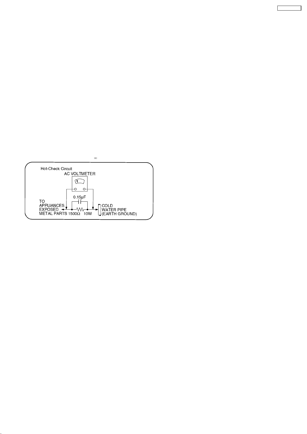
3. After servicing, make the following leakage current checks to prevent the customer from being exposed to shock hazards.
1.1.1. Leakage current cold check
1. Unplug the AC cord and connect a jumper between the two
prongs on the plug.
2. Measure the resistance value, with an ohmmeter, between
the jumpered AC plug and each exposed metallic cabinet
part on the equipment such as screwheads, connectors,
control shafts, etc. When the exposed metallic part has a
return path to the chassis, the reading should be between
1MW and 5.2MW.
When the exposed metal does not have a return path to the
chassis, the reading must be
.
Figure 1
1.1.2. Leakage current hot check
(See Figure 1 .)
1. Plug the AC cord directly into the AC outlet. Do not use an
isolation transformer for this check.
2. Connect a 1.5kW, 10 watts resistor, in parallel with a 0.15µF
capacitors, between each exposed metallic part on the set
and a good earth ground such as a water pipe, as shown in
Figure 1.
3. Use an AC voltmeter, with 1000 ohms/volt or more
sensitivity, to measure the potential across the resistor.
4. Check each exposed metallic part, and measure the
voltage at each point.
5. Reverse the AC plug in the AC outlet and repeat each of the
above measurements.
6. The potential at any point should not exceed 0.75 volts
RMS. A leakage current tester (Simpson Model 229 or
equivalent) may be used to make the hot checks, leakage
current must not exceed 1/2 milliampere. In case a
measurement is outside of the limits specified, there is a
possibility of a shock hazard, and the equipment should be
repaired and rechecked before it is returned to the
customer.
3
Page 4
DMR-EX80SEG
2 Warning
2.1. Prevention of Electrostatic Discharge (ESD) to Electrostatic Sensitive
(ES) Devices
Some semiconductor (solid state) devices can be damaged easily by static electricity. Such components commonly are called
Electrostatic Sensitive (ES) Devices. Examples of typical ES devices are integrated circuits and some field-effect transistor-sand
semiconductor "chip" components. The following techniques should be used to help reduce the incidence of component damage
caused by electrostatic discharge (ESD).
1. Immediately before handling any semiconductor component or semiconductor-equipped assembly, drain off any ESD on your
body by touching a known earth ground. Alternatively, obtain and wear a commercially available discharging ESD wrist strap,
which should be removed for potential shock reasons prior to applying power to the unit under test.
2. After removing an electrical assembly equipped with ES devices, place the assembly on a conductive surface such as
aluminum foil, to prevent electrostatic charge buildup or exposure of the assembly.
3. Use only a grounded-tip soldering iron to solder or unsolder ES devices.
4. Use only an anti-static solder removal device. Some solder removal devices not classified as "anti-static (ESD protected)" can
generate electrical charge sufficient to damage ES devices.
5. Do not use freon-propelled chemicals. These can generate electrical charges sufficient to damage ES devices.
6. Do not remove a replacement ES device from its protective package until immediately before you are ready to install it. (Most
replacement ES devices are packaged with leads electrically shorted together by conductive foam, aluminum foil or comparable
conductive material).
7. Immediately before removing the protective material from the leads of a replacement ES device, touch the protective material
to the chassis or circuit assembly into which the device will be installed.
Caution
Be sure no power is applied to the chassis or circuit, and observe all other safety precautions.
8. Minimize bodily motions when handling unpackaged replacement ES devices. (Otherwise harmless motion such as the
brushing together of your clothes fabric or the lifting of your foot from a carpeted floor can generate static electricity sufficient
to damage an ES device).
4
Page 5
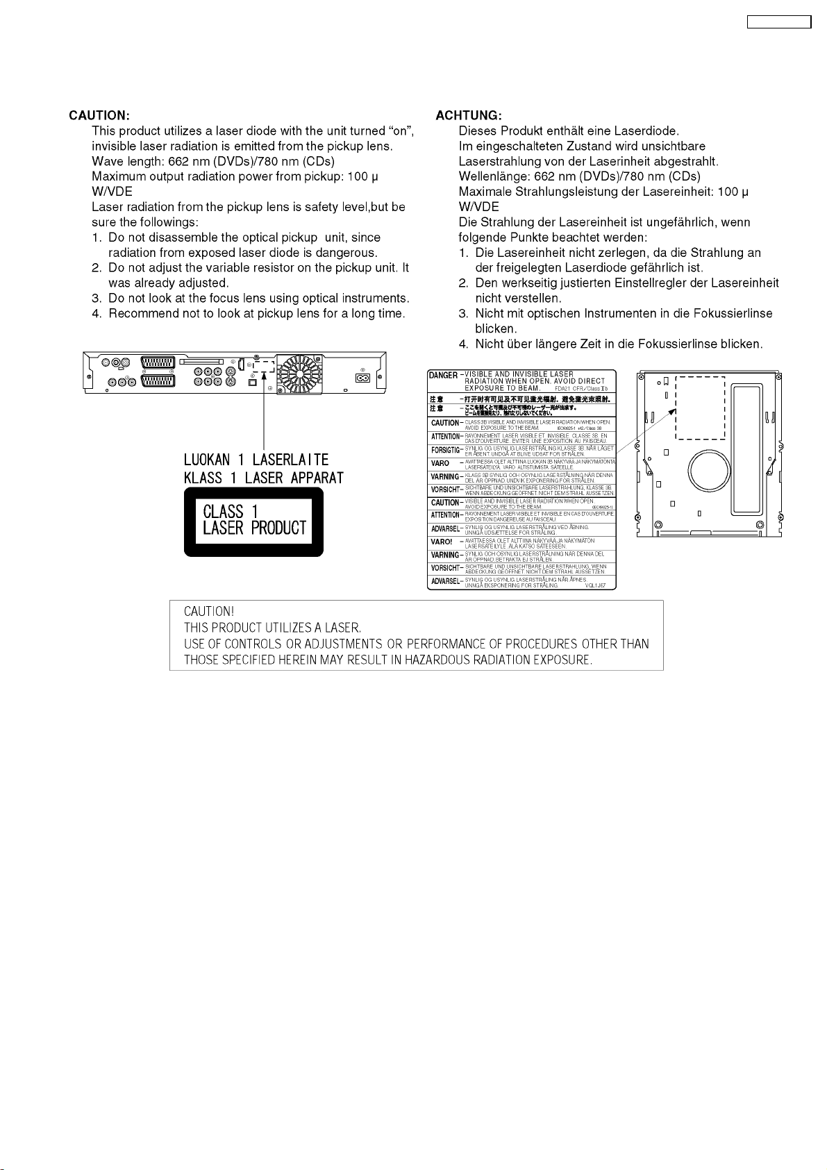
2.2. Precaution of Laser Diode
DMR-EX80SEG
5
Page 6

DMR-EX80SEG
2.3. Service caution based on legal restrictions
2.3.1. General description about Lead Free Solder (PbF)
The lead free solder has been used in the mounting process of all electrical components on the printed circuit boards used for this
equipment in considering the globally environmental conservation.
The normal solder is the alloy of tin (Sn) and lead (Pb). On the other hand, the lead free solder is the alloy mainly consists of tin
(Sn), silver (Ag) and Copper (Cu), and the melting point of the lead free solder is higher approx.30 degrees C (86°F) more than that
of the normal solder.
Definition of PCB Lead Free Solder being used
The letter of “PbF” is printed either foil side or components side on the PCB using the lead free solder.
(See right figure)
Service caution for repair work using Lead Free Solder (PbF)
·
The lead free solder has to be used when repairing the equipment for which the lead free solder is used.
(Definition: The letter of “PbF” is printed on the PCB using the lead free solder.)
·
To put lead free solder, it should be well molten and mixed with the original lead free solder.
·
Remove the remaining lead free solder on the PCB cleanly for soldering of the new IC.
·
Since the melting point of the lead free solder is higher than that of the normal lead solder, it takes the longer time to melt
the lead free solder.
·
Use the soldering iron (more than 70W) equipped with the temperature control after setting the temperature at 350±30
degrees C (662±86°F).
Recommended Lead Free Solder (Service Parts Route.)
·
The following 3 types of lead free solder are available through the service parts route.
RFKZ03D01K-----------(0.3mm 100g Reel)
RFKZ06D01K-----------(0.6mm 100g Reel)
RFKZ10D01K-----------(1.0mm 100g Reel)
Note
* Ingredient: tin (Sn), 96.5%, silver (Ag) 3.0%, Copper (Cu) 0.5%, Cobalt (Co) / Germanium (Ge) 0.1 to 0.3%
6
Page 7
3 Service Navigation
3.1. Service Information
DMR-EX80SEG
3.2. Caution for DivX
7
Page 8
DMR-EX80SEG
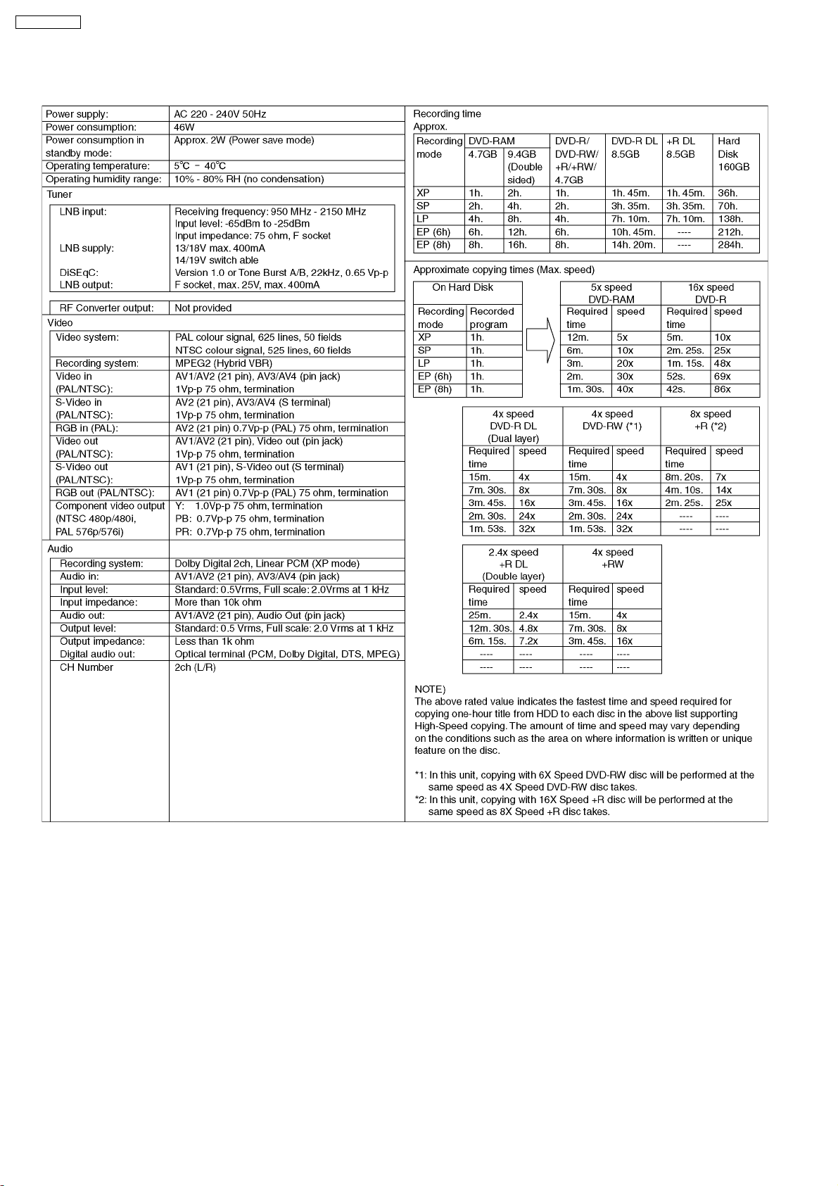
4 Specifications
8
Page 9
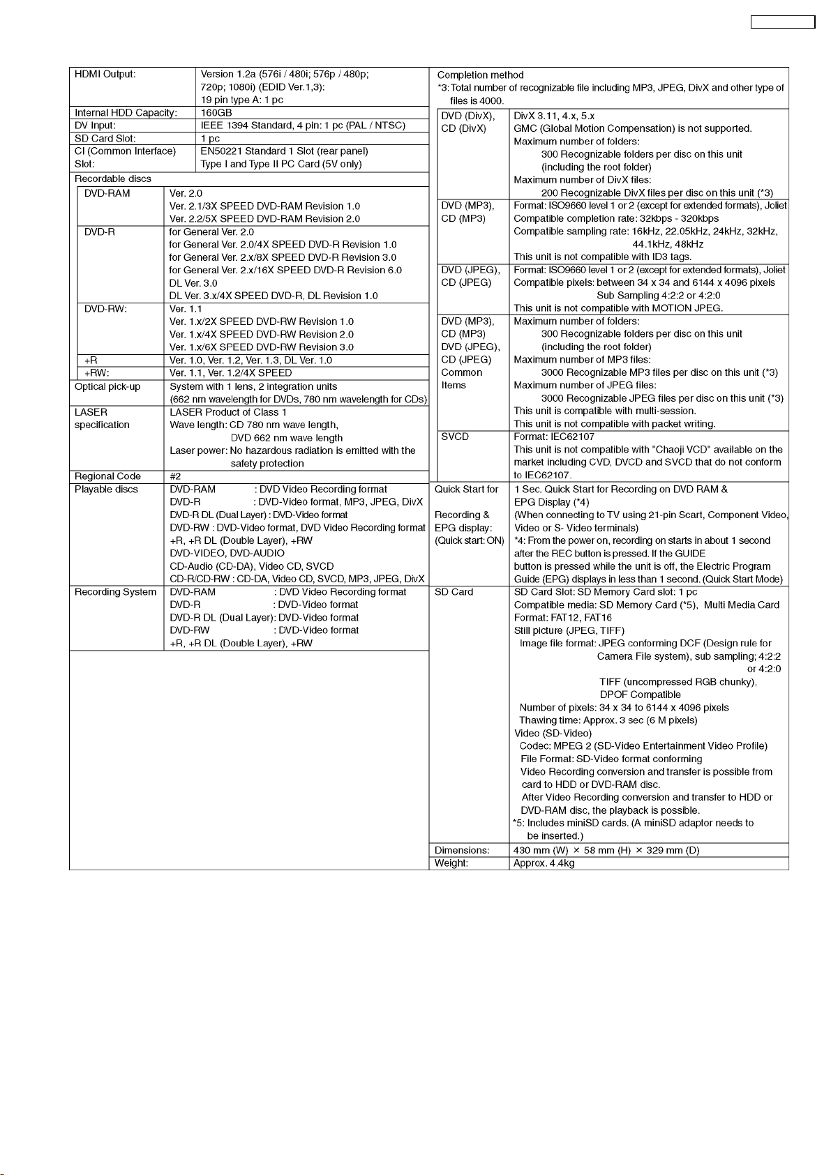
DMR-EX80SEG
9
Page 10
DMR-EX80SEG
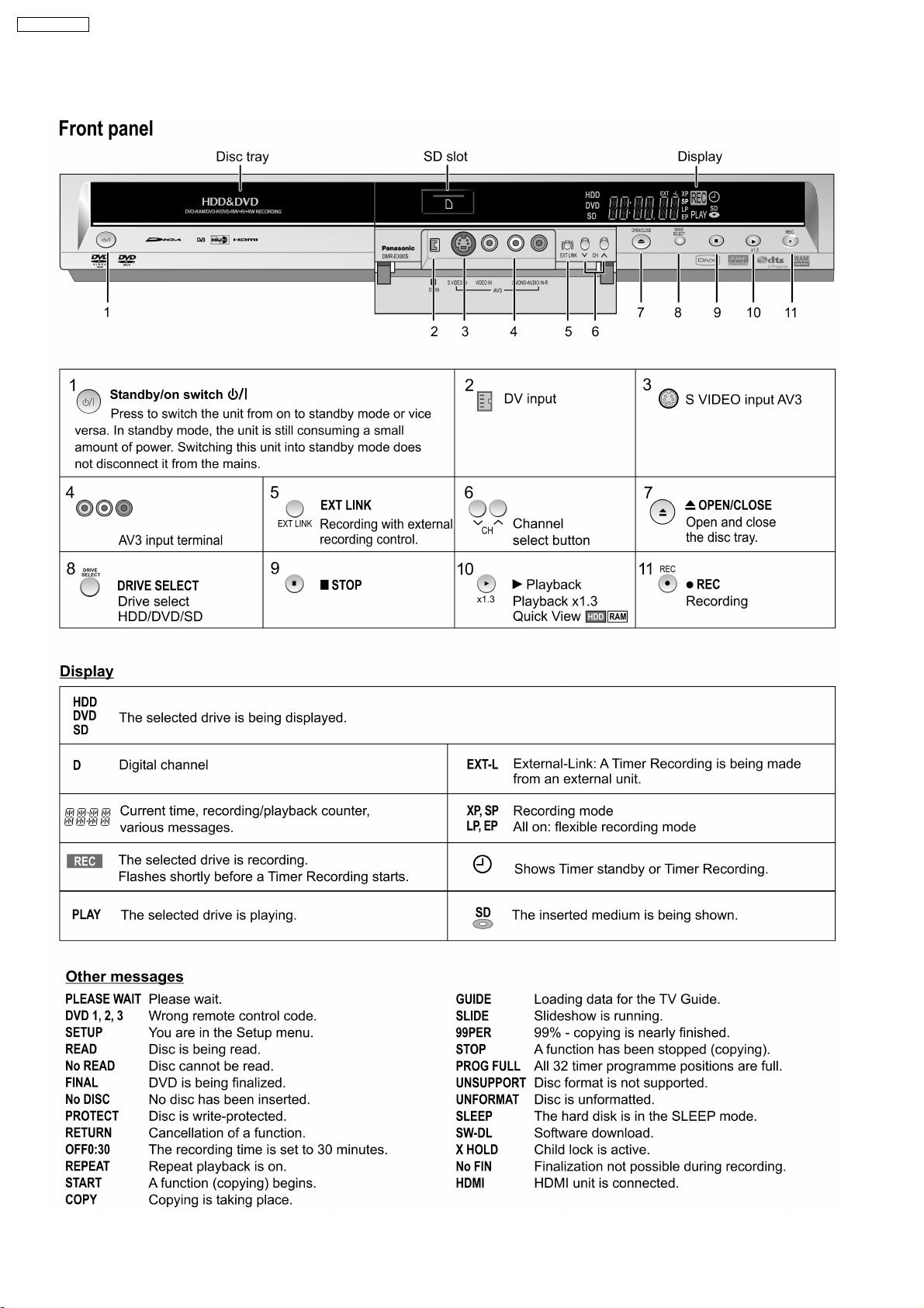
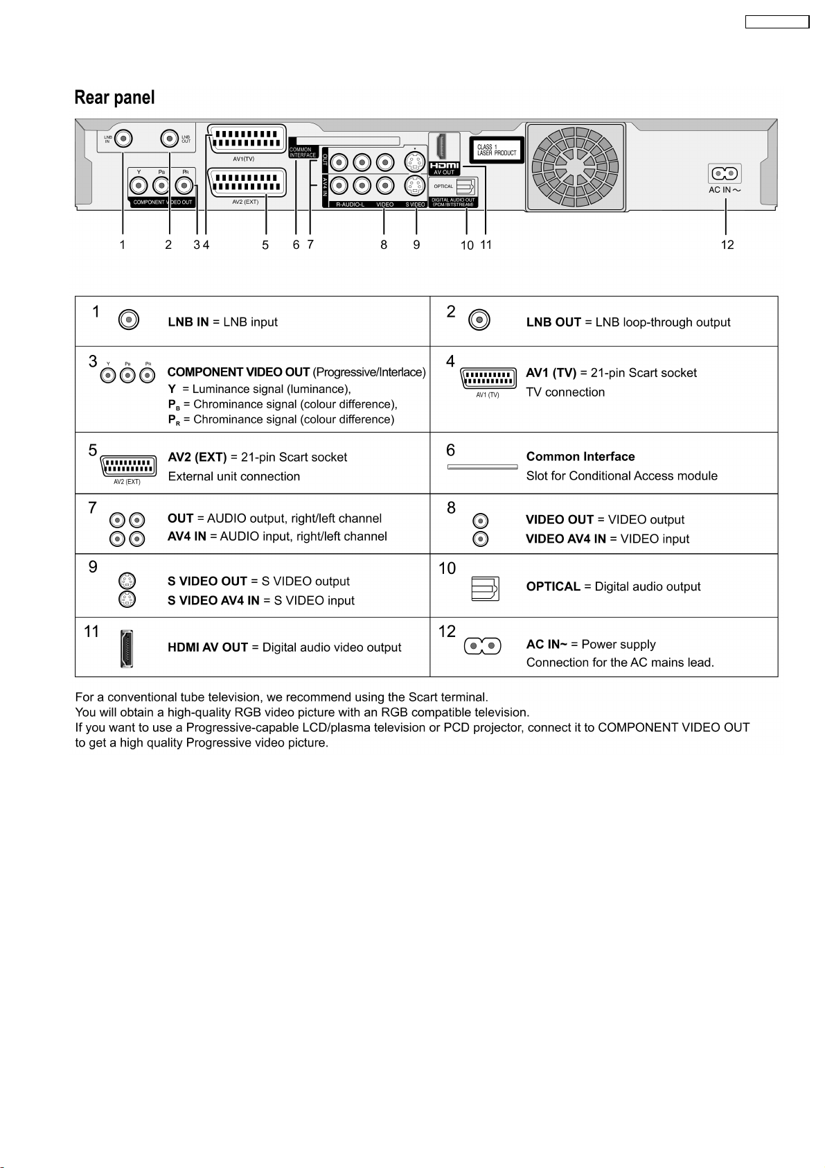
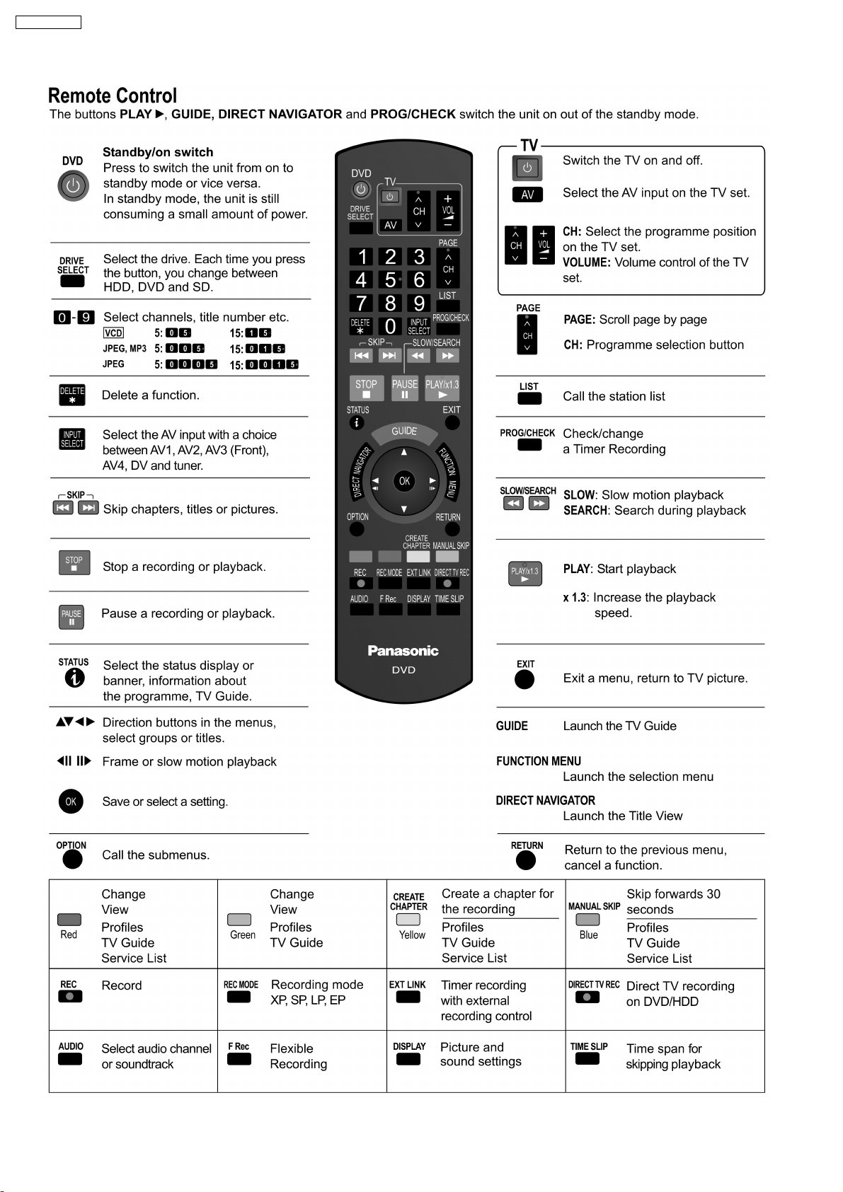
5 Location of Controls and Components
10
Page 11
DMR-EX80SEG
11
Page 12
DMR-EX80SEG
12
Page 13
DMR-EX80SEG
6 Operation Instructions
6.1. Taking out the Disc from DVD-Drive Unit when the Disc cannot be
ejected by OPEN/CLOSE button
6.1.1. Forcible Disc Eject
6.1.1.1. When the power can be turned off.
1. Turn off the power and press [STOP] [CH UP] keys on the front panel simultaneously for 5 seconds.
6.1.1.2. When the power can not be turned off.
1. Press [POWER] key on the front panel for over 10 seconds to turn off the power forcibly, and press [STOP] [CH UP] keys on
the front panel simultaneously for 5 seconds.
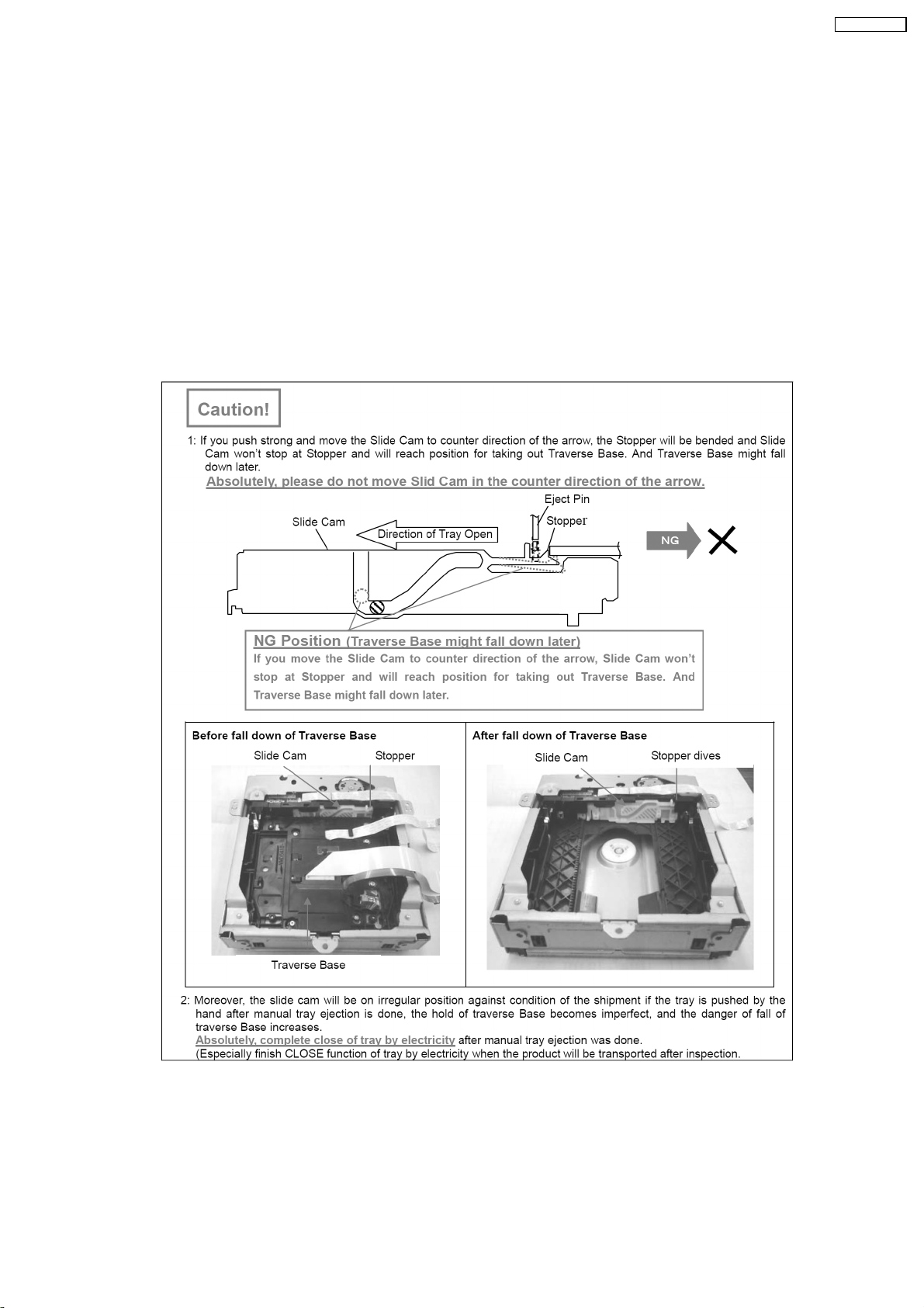
6.1.2. When the Forcible Disc Eject can not be done.
13
Page 14
DMR-EX80SEG
1. Turn off the power and pull out AC cord.
2. Remove the Top Case.
3. Put deck so that bottom can be seen.
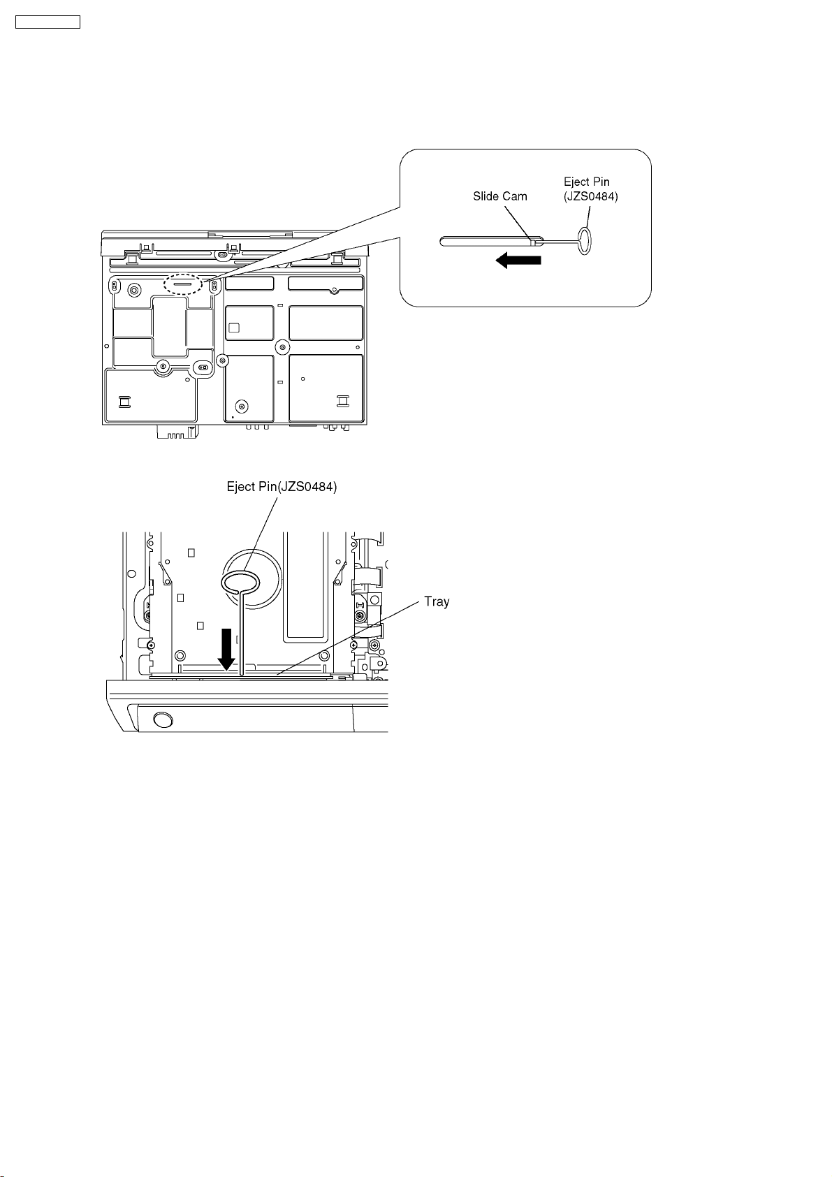
4. Slide SLIDE CAM by Eject Pin (JZJ0484) or minus screw driver (small) in the direction of arrow to eject tray slightly.
5. Put deck upward, and push out Tray by Eject Pin (JZS0484) or minus screw driver (small).
14
Page 15
DMR-EX80SEG
7 Service Mode
7.1. Self-Diagnosis and Special Mode Setting
7.1.1. Self-Diagnosis Functions
Self-Diagnosis Function provides information for errors to service personnel by “Self-Diagnosis Display” when any error has
occurred.
U**, H** and F** are stored in memory and held.
You can check latest error code by transmitting [0] [1] of Remote Controller in Service Mode.
Automatic Display on FL will be cancelled when the power is turned off or AC input is turned off during self-diagnosis display is ON.
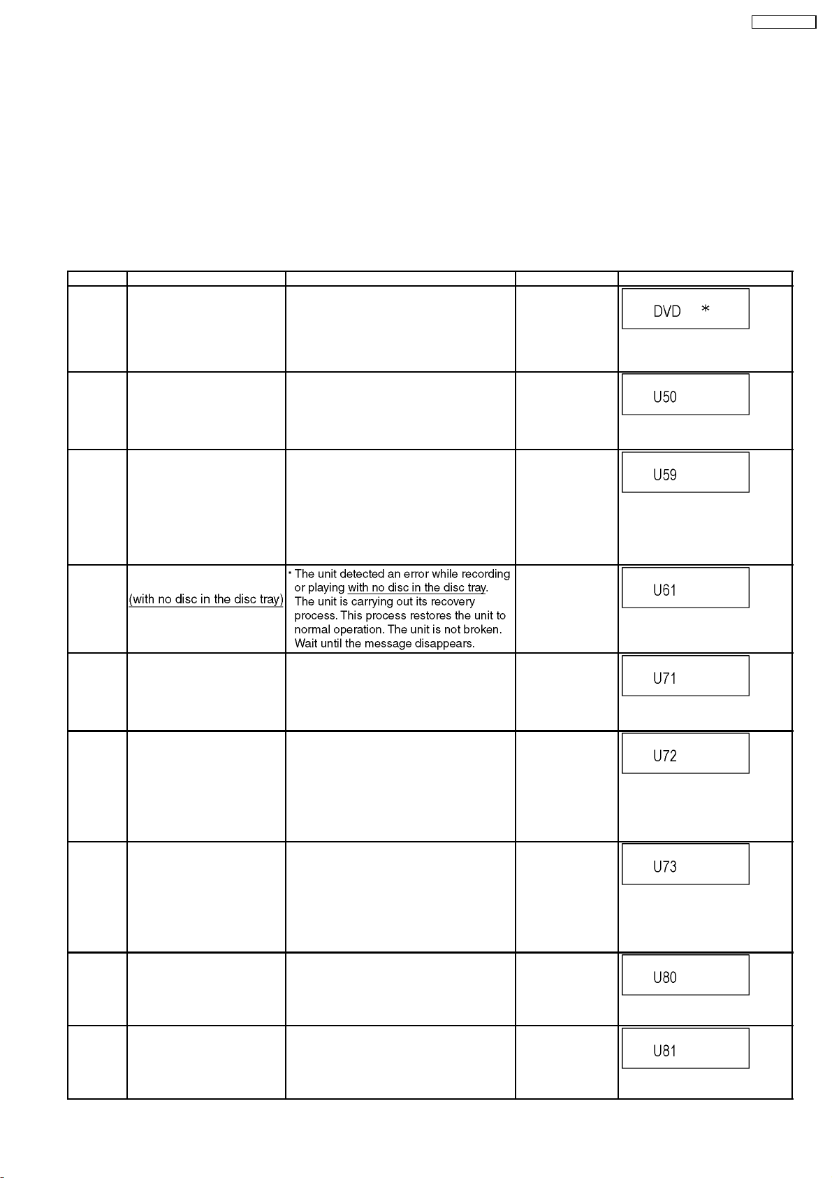
Error Code Diagnosis contents Description Monitor Display Automatic FL display
U30 Remote control code error Display appears when main unit and remote
U50 Antenna Short U50 is displayed when a short circuit was
U59 Abnormal inner temperature
detected
U61 The unit is carrying out its
recovery process.
controller codes are not matched.
detected at Antenna Input while "Active
Antenna” of “Connection” of “Setup” of
“ToOthers” of “FUNCTION MENU” is ON, And
then “Active Antenna” is compulsorily
switched to “Off”.
Display appears when the drive temperature
exceeds 70°C.
The power is turned off forcibly.
For 30 minutes after this, all key entries are
disabled. (Fan motor operates at the highest
speed for the first 5 minutes. For the
remaining 25 minutes, fan motor is also
stopped.) The event is saved in memory as
well.
No display
“*” is remote controller code of the
main unit.
Display for 5 seconds.
“A short circuit was
detected at the
antenna input.
Please check your
antenna.”
No display
“U59 is displayed for 30 minutes.
No display
U71 HDMI incompatible error
(HDCP incompatible)
U72 HDMI connection error
(communication error)
U73 HDMI connection error
(authentication error)
U80 ST Microprocessor
Communication Error on Timer
Bus
U81 ST Microprocessor
Communication Error on UART
Display this error when the equipment
(compatible with DVI such as TV, amplifier
etc.) connected to the unit by HDMI is
incompatible with HDCP.
*HDCP=High-bandwidth Digital Content
Protection
This error is displayed when there are any
communication problems with the unit and the
equipments (TV, amplifier etc.) connected to
the unit by HDMI. (or when there is a problem
with the HDMI cable)
When authentication error occurs while the
equipments (TV, amplifier etc.) are connected
by HDMI. (or when there is a problem with the
HDMI cable)
Display appears when ST Microprocessor
Communication Error on Timer Bus occurs.
Display appears when ST Microprocessor
Communication Error on DART occurs.
No display
U72 display disappears when
error has been solved by Power
OFF/ON of connecting equipment
or by inserting/removing of HDMI
cable.
No display
U72 display disappears when
error has been solved by Power
OFF/ON of connecting equipment
or by inserting/removing of HDMI
cable.
No display
"U80" is displayed till Power Key is
pressed.
No display
15
"U81" is displayed till Power Key is
pressed.
Page 16
DMR-EX80SEG
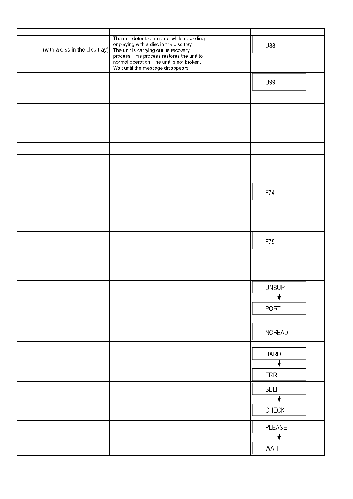
Error Code Diagnosis contents Description Monitor Display Automatic FL display
U88 The unit is carrying out its
No display
recovery process.
U99 Hang-up Displayed when communication error has
occurred between Main microprocessor and
Timer microprocessor.
H19 Inoperative fan motor When inoperative fan motor is detected after
powered on, the power is turned off
automatically.
The event is saved in memory.
F00 No error information Initial setting for error code in memory
(Error code Initialization is possible with error
code initialization and main unit initialization.)
F58 Drive hardware error When drive unit error is detected, the event is
saved in memory.
F34 Initialization error when main
microprocessor is started up
for program recording
When initialization error is detected after
starting up main microprocessor for program
recording, the power is turned off
automatically.
The event is saved in memory.
F74 HDIM Device Key
Communication error.
HDMI connection could not be authenticated
due to a transfer malfunction.
Factor of HDMI Device key-road failure
·
When HDMI LSI is damaged.
·
When the bus line of I2C doesn´t operate
normally.
·
When device key information recorded is
damaged.
F75 HDIM Device Key Information
error
HDMI connection could not be authenticated
due to an internal data malfunction.
Factor of HDMI Device key-road failure
·
When HDMI LSI is damaged.
·
When the bus line of I2C doesn´t operate
normally.
·
When device key information recorded is
damaged.
UNSUPPORTUnsupported disc error *An unsupported format disc was played,
although the drive starts normally.
*The data format is not supported, although
the media type is supported.
*Exceptionally in case of the disc is dirty.
No display
Displayed is left until the
[POWER] key is pressed.
No display No display
No display No display
No display No display
No display No display
No display
No display
“This disc is
incompatible.”
NO READ Disc read error *A disc is flawed or dirty.
*A poor quality failed to start.
*The track information could not be read.
HARD
Drive error The drive detected a hard error. “DVD drive error.” Display for 5 seconds.
ERR
SELF
CHECK
Restoration operation Since the power cord fell out during a power
failure or operation, it is under restoration
operation.
*It will OK, if a display disappears
automatically. If a display does not disappear,
there is the possibility that defective Digital
P.C.B. / RAM drive.
PLEASE
WAIT
Unit is in termination process Unit is in termination process now.
“BYE” is displayed and power will be turned
off.
In case “Quick Start” of setup menu is ON, it
is displayed in restoration operation for AC
off.
Display for 5 seconds.
“Cannot read.
Please check the
disc.”
No display
No display
16
Page 17
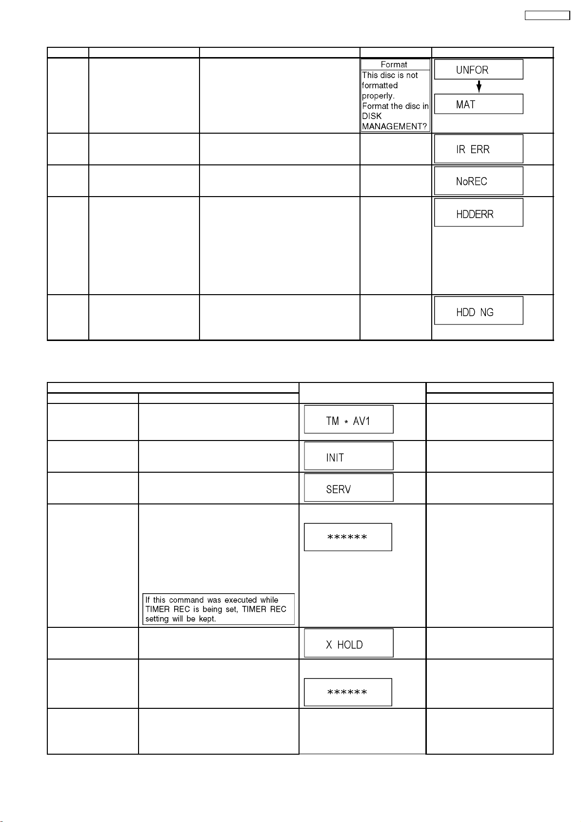
Error Code Diagnosis contents Description Monitor Display Automatic FL display
UNFORMATUnformatted disc error You have inserted an unformatted DVD-RAM
or DVD-RW that is unformatted or recorded
on other equipment.
DMR-EX80SEG
IR ERR IR communication error [IR ERR] is displayed when communication
No REC Recording is impossible [No REC] is displayed when recording is
HDD
ERROR
HDD NG Power on Stand-by setting
[HDD ERR] is displayed when
start up of HDD was failed.
(Except error of setting of
Power on Stand-by)
error
between Timer microprocessor and IR
microprocessor fails.
impossible due to the defect, dirt or wound of
media.
a) When normal start up was failed.
b) When start up at HDD boot was failed.
c) When start up from state of P-OFF was
failed.
d) When start up from state of HDD SLEEP
was failed.
[HDD ERR] is displayed when above each
start up of HDD was failed.
*In case b), tray opens automatically and
[HDDERR] is displayed until version up disc is
inserted.
[HDD NG] is displayed when power on Standby setting of HDD is NG or when HDD which
power on Stand-by is not set to is used.
Please try to replace HDD with junine HDD as
service parts.
No display
No display
No display
No display
7.1.2. Special Modes Setting
Item FL display Key operation
Mode name Description Front Key
TEST Mode *All the main unit´s parameters (include tuner)
are initialized.
Rating password The audiovisual level setting password is
initialized to “Level 8”.
Service Mode Setting every kind of modes for servicing.
*Details are described in “7.1.3. Service
Mode at a glance”.
Forced disc eject Removing a disc that cannot be ejected.
The tray will open and unit will shift to P-off
mode.
*When Timer REC is ON or EXT-LINK is ON,
execute " Forced disc eject " after releasing
Timer REC or EXT-LINK.
*This command is not effective during "Child
lock" is ON.
While Demonstration Lock is being set, this
Forced disc eject function is not accepted.
The display before execution
leaves.
Press [STOP], [CH UP] and
[OPEN/CLOSE] keys
simultaneously for five seconds
when power is off.
Open the tray, and press [REC] and
[PLAY] simultaneously for 5
seconds.
When the power is off, press [CH
UP], [OPEN/CLOSE] and [REC]
keys simultaneously for 5 seconds.
When the power is off, press
[STOP] and [CH UP] keys
simultaneously for 5 seconds.
Child lock/unlock Set or release “Child Lock”. Press [ENTER] and [RETURN] by
NTSC/PAL system select To switch PAL/NTSC altemately. The display before execution
Forced power-off When the power button is not effective while
power is ON, turn off the power forcibly.
*When Timer REC is ON or EXT-LINK is ON,
execute “Forced Power-off” after releasing
Timer REC or EXT-LINK.
leaves.
Display in P-off mode. Press [Power] key over than 10
remote controller simultaneously
until [X-HOLD] is displayed.
While the power is on (E-E mode),
press [STOP] and [OPEN/CLOSE]
simultaneously for 5 seconds.
seconds.
17
Page 18
DMR-EX80SEG
Item FL display Key operation
Mode name Description Front Key
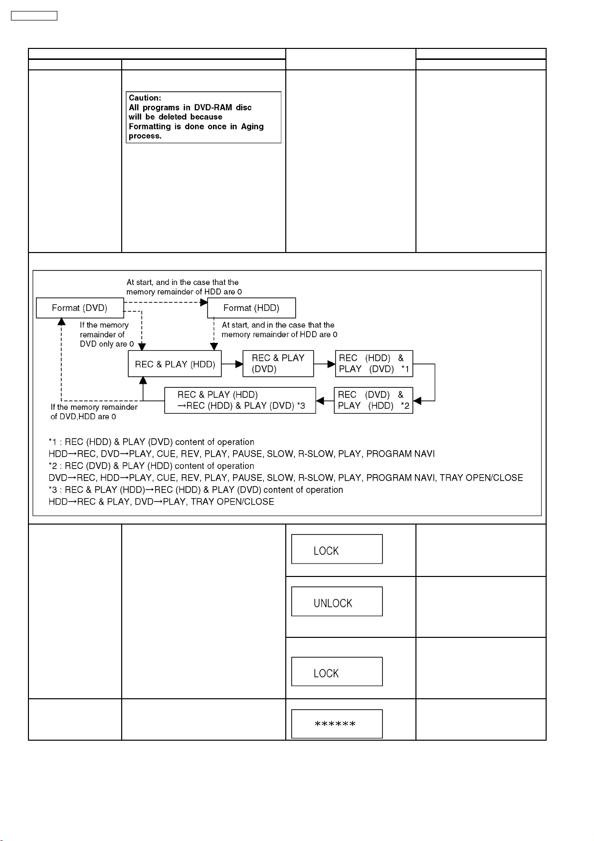
Aging Perform sequence of modes as * Aging
Description shown below continually.
Display following the then mode. When the power is ON, press
[STOP], [POWER] and
[OPEN/CLOSE] simultaneously for
over 5 seconds and less than 10
seconds.
NOTE1:
If Unit has not turned into Aging
mode by operations shown above,
execute TEST MODE once and reexecute operation shown above.
(*All the main unit’s parameters
include tuner are initialized by TEST
mode.)
NOTE2:
If the unit has hung-up because of
pressing keys for over 10 seconds,
once turn off the power, and reexecute this command.
*When releasing Aging mode, press
[POWER] key.
Aging Contents (Example):
Demonstration
lock/unlock
ATP re-execution Re-execute ATP. Display at ATP executing. When the power is on (E-E mode),
Ejection of the disc is prohibited.
The lock setting is effective until unlocking the
tray and not released by “Main unit
initialization” of service mode.
*When lock the tray.
“LOCK” is displayed for 3 seconds.
*When unlock the tray.
“UNLOCK” is displayed for 3
seconds.
*When press OPEN/CLOSE key
while the tray being locked.
Display “LOCK” for 3 seconds.
When the power is on, press
[STOP] and [POWER] keys
simultaneously for 5 seconds.
When the power is on, press
[STOP] and [POWER] keys
simultaneously for 5 seconds.
Press [OPEN/CLOSE] key while the
tray being locked.
press [CH UP] and [CH DOWN]
simultaneously for 5 seconds.
18
Page 19
DMR-EX80SEG
Item FL display Key operation
Mode name Description Front Key
Progressive initialization The progressive setting is initialized to
Interlace.
The display before execution
leaves.
When the power is on (E-E mode),
press [STOP] and [PLAY]
simultaneously for 5 seconds.
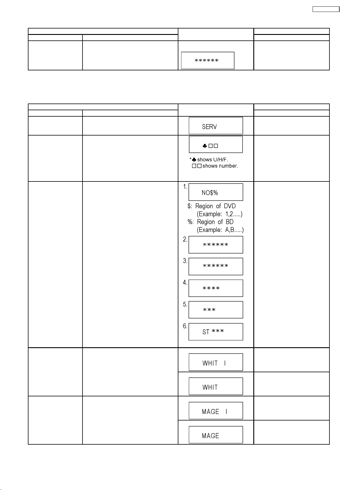
7.1.3. Service Modes at a glance
Service mode setting: While the power is off, press REC, CH UP and OPEN / CLOSE simultaneously for five seconds.
Item FL display Key operation
Mode name Description (Remote controller key)
Release Items Item of Service Mode executing is cancelled. Press [0] [0] or [Return] in service
mode.
Error Code Display Last Error Code of U/H/F held by Timer is
displayed on FL.
*Details are described in “7.1.1. Self-
Diagnosis Functions”.
ROM Version Display 1. Region code (displayed for 5 sec.)
2. Main firm version (displayed for 5 sec.)
3. Timer firm version (displayed for 5 sec.)
4. Drive firm version (displayed for 5 sec.)
5. ROM correction version (displayed for 5
sec.)
6. ST Microprocessor version (left displayed)
Press [0] [1] in service mode
If any error history does not exist,
[F00] is displayed.
Press [0] [2] in service mode
White Picture Output White picture is output as component Output
from AV Decoder.
*White picture
(Saturation rate : 100%)
*It is enable to switch Interlace/Progressive by
“I/P switch: [1] [4]”
Magenta Picture Output Magenta picture is output with Component
Output from AV Decoder.
*Magenta picture
(Saturation rate: 100%)
*It is enable to switch Interlace/Progressive by
“I/P switch: [1] [4]”
‘’ * ’’ are version displays.
*Initial mode is “Interlace”. Press [1] [1] in service mode.
Switch Interlace/Progressive Press [1] [4] in White Picture Output
mode.
*I/P are switched alternately.
*Initial mode is “Interlace”. Press [1] [2] in service mode.
Switch Interlace/Progressive Press [1] [4] in Magenta Picture
Output mode.
*I/P are switched alternately.
19
Page 20
DMR-EX80SEG
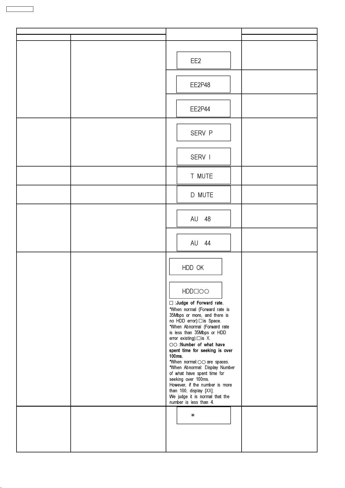
Mode name Description (Remote controller key)
RTSC Return in XP
(A & V)
Item FL display Key operation
AV1 input signal is encoded (XP), decoded
(XP) and output decoded signal to external
Initial mode: EE2/ Interlace/ XP/
Audio 48kHz
Press [1] [3] in service mode.
without DISC recording and DISC playback.
I/P Switch Switch Interlace and Progressive in EE mode.
*Initial setting is “Interlace”.
*This command is effective during executing
“White Picture Output”, “Magenta Picture
Output” and “RTSC Return in XP (A & V)”
modes.
Audio Mute (XTMUTE) Check whether mute is applied normally by
the timer microprocessor.
Audio Mute (XDMUTE) Check whether mute is applied normally by
the Digital P.C.B..
Audio Pattern Output The audio pattern stored in the internal
memory is output
(Lch: 1kHz/-18dB)
(Rch: 400Hz/-18dB)
*Audio sound clock switching operation of
DAC can be confirmed by sub command [2]
[4].
HDD READ inspection Perform a complete read inspection of the
HDD.
Switch Interlace/Progressive Press [1] [4] in RTSC Return XP
mode.
*I/P are switched alternately.
Audio 44.1 kHz/ 48 kHz Switch Press [2] [4] in RTSC Return XP
mode.
*48 kHz / 44.1 kHz are switched
alternately.
Initial mode is Interlace
Press [1] [4] in I/P Switch mode.
*I/P are switched alternately.
Switch Interlace/Progressive
Press [2] [1] in service mode.
Press [2] [2] in service mode.
Initial mode (Audio 48kHz) Press [2] [3] in service mode.
Audio 44.1kHz/48kHz switching Press [2] [4] in Audio Pattern Output
mode.
*48 kHz / 44.1 kHz are switched
alternately.
When the HDD is OK
Press [3] [1] in service mode.
*When canceling the checking
mode while executing, do “forced
power-off”.
If the HDD is defective
Method:
Press the “POW ER” button more
than 10 seconds.
Laser Used Time
Indication
Check laser used time (hours) of drive.
Press [4] [1] in service mode.
l(*****) is the used time display in
hour.
lLaser used time of DVD/ CD in
Playback/Recording mode is
counted.
20
Page 21
Item FL display Key operation
Mode name Description (Remote controller key)
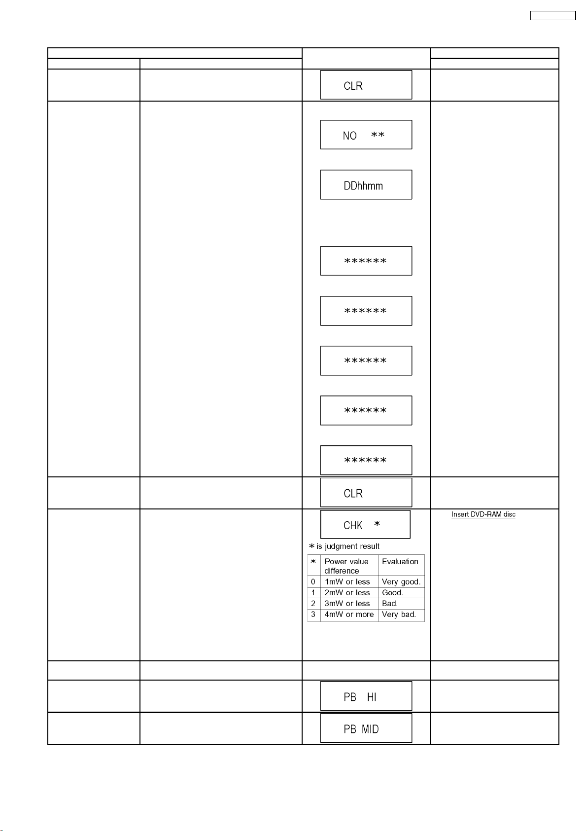
Delete the Laser Used
Time
Laser used time stored in the memory of the
unit is deleted.
Press [9] [5] in service mode.
DMR-EX80SEG
RAM Drive Last Error RAM Drive error code display.
*For details about the drive error code, refer
to the Service Manual for the specific RAM
Drive.
1. Error Number is displayed for 5
seconds.
2. Time when the error has occurred
is displayed for 5 seconds.
DD: Day
hh: Hour
mm: Minute
3. Last Drive Error (1/2) is displayed
for 5 seconds.
4. Last Drive Error (2/2) is displayed
for 5 seconds.
5. Error occurring Disc type is
displayed for 5 seconds.
6. Disc Maker ID is displayed for 5
seconds.
Press [4] [2] in service mode.
When “INFO******” is being
displayed, past 19 error histories
can be displayed by pressing [0] [1]
- [1] [9]
In case that the maker cannot be
identified, display is black out.
Delete the Last Drive
Error
Delete the Last Drive Error information stored
on the DVD RAM-Drive.
Laser power confirmation Drive state is judged based on difference
between laser power value at shipping and
present laser power value.
Turn on all FL/LEDs All segments of FL and all LEDs are turned
on.
PB HIGH Signal Output 8 pin of AV 1 Jack (PB HIGH terminal) is High
(approx. 11V DC).
PB MIDDLE Signal
Output
8 pin of AV 1 Jack (PB HIGH terminal) is
Middle (approx. 5.5V DC)
7. Factor of Drive Error occurring is
left displayed
Press [9] [6] in service mode.
1. into RAM
Drive in service mode. (Other
media are assumed to be noncorrespondence.)
2. Press [4] [4].
If DVD-RAM disc in not inserted,
[NO DISC] is displayed.
If power value study was filed,
[ERROR] is displayed.
All segments are turned on. Press [5] [1] in service mode.
Press [5] [2] in service mode.
Press [5] [3] in service mode.
21
Page 22
DMR-EX80SEG
Item FL display Key operation
Mode name Description (Remote controller key)
Front connection
inspection
Production Date Display Display the date when the unit was produced.
Display the accumlated
working time
Display the Error History Display the Error History stored on the unit. Display reason of error for 5
Press all front keys and check the connection
between Main P.C.B. and Front key Switches.
(1) Each time a key is pressed,
segment turned on increases one
by one.
(2) Total number of keys that have
been pressed.
YY: Year
MM: Month
DD: Day
Display the accumulated unit´s working time.
(Indicating unit: Second)
seconds.
Press [5] [4] in service mode.
Press [6] [1] in service mode.
Press [6] [4] in service mode.
Press [6] [5] in service mode.
Then press [0] [1] ~ [1] [9], the past
19 error histories are displayed.
Delete the Error History Delete Error History information stored on the
unit.
01:
Defect of Digital P.C.B.
(AV DEC / MAIN CPU)
02:
Defect of RAM Drive.
03:
Defect of Disc.
04:
Defect of Digital P.C.B. or
Communication Error.
05:
Defect of Digital P.C.B.
(AV DEC / MAIN CPU)
06:
Defect of HDD.
Display the time when the error has
occurred for 5 seconds.
DD: Day
hh: Hour
mm: Minute
Accumulated working time till
occuring of the error is left
displayed.
(Indicating unit: Second)
Press [9] [7] in service mode.
SD card WRITE check Delete Error History information stored on the
unit.
When the WRITE check is OK.
When the WRITE check is NG.
*Note:
The image stored in the SD card will
be erased.
22
Insert a SD card to SD card slot,
and press [7] [4] in service mode.
*Insert SD card while the power is
off.
*Check for [CARD SD] display on
the FL display and go on the
procedure.
Page 23
Item FL display Key operation
Mode name Description (Remote controller key)
AV4(V)/AV1(RGB) I/O
Setting
Set input to AV4 (V) and set output to AV1
(RGB) for I/O checking
Press [8] [0] in service mode.
DMR-EX80SEG
AV2(Y/C)/AV1(V) I/O
Setting
AV2(V)/AV1(Y/C) I/O
Setting
AV2(RGB)/AV1(V) I/O
Setting
Set input to AV2 (Y/C) and set output to AV1
(V) for I/O checking
Set input to AV2 (V) and set output to AV1
(Y/C) for I/O checking
Set input to AV2 (RGB) and set output to AV1
(V) for I/O checking
P50(H) Output Timer Microprocessor IC7501-76 output High
signal for AV1-pin 10 passing through inverter
(approx. 0V DC at AV1-pin 10).
P50(L) Output Timer Microprocessor IC7501-76 output Low
signal for AV1-pin 10 passing through inverter
(approx. 4.4V DC at AV1-pin 10).
Tray OPEN/CLOSE Test The RAM drive tray is opened and closed
repeatedly.
Error code initialization Initialization of the last error code held by
timer (Write in F00)
When OK.
When NG.
When OK.
When NG.
“*” is number of open/close cycle
times.
Press [8] [1] in service mode.
Press [8] [2] in service mode.
Press [8] [3] in service mode.
Press [8] [4] in service mode.
Press [8] [5] in service mode.
Press [9] [1] in service mode
*When releasing this mode, press
the [POWER] button of Remote
Controller more than 10 seconds.
Press [9] [8] in service mode.
Initialize Service Last Drive Error, Error history and Error
Press [9] [9] in service mode.
Codes stored on the unit are initialized to
factory setting.
Finishing service mode Release Service Mode. Display in STOP (E-E) mode. Press power button on the front
panel or Remote controller in
service mode.
23
Page 24

DMR-EX80SEG
8 Service Fixture & Tools
Part Number Description Compatibility
RFKZ0260 Extension Cable (MainP.C.B. - RAM/Digital P.C.B. Module/ 88 Pin) Same as EH50 Series
RFKZ0216 Extension Cable (MainP.C.B. - Power P.C.B./ 23 Pin) Same as E55 Series
RFKZ0366 Extension FFC (HDD - RAM/Digital P.C.B. Module/ 40 Pin) Same as EH55 Series
RFKZ0168 Extension Cable (Power P.C.B. - Fan Motor/ 3 Pin) Same as E50/ E55 Series
RFKZ0339 Extension Cable (MainP.C.B. - HDD / 4 Pin) Same as EH55 Series
RFKZ0458 Extension Cable (Power P.C.B. - SAT Main P.C.B. / 6 Pin) New
JZS0484 Eject Pin Same as E50 Series
RFKZ03D01K Lead Free Solder (0.3mm/100g Reel) Same as EH55 Series
RFKZ06D01K Lead Free Solder (0.6mm/100g Reel) Same as EH55 Series
RFKZ10D01K Lead Free Solder (1.0mm/100g Reel)) Same as EH55 Series
RFKZ0316 Solder Remover (Lead free 10W temperature Solder/180g) Same as EH55 Series
RFKZ0328 Flux Same as EH55 Series
RFKZ0329 Bottle of Flux Same as EH55 Series
24
Page 25
DMR-EX80SEG
9 Disassembly and Assembly Instructions
9.1. Disassembly Flow Chart
The following chart is the procedure for disassembling the casing and inside parts for internal inspection when carrying out the
servicing.
To assemble the unit, reverse the steps shown in the chart below.
25
Page 26
DMR-EX80SEG
9.2. P.C.B. Positions
26
Page 27
DMR-EX80SEG
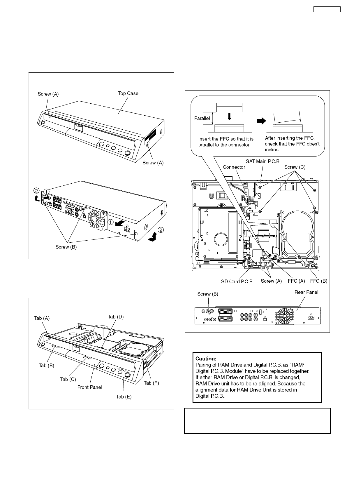
9.3. Top Case
1. Remove 2 Screws (A) and 3 Screws (B).
2. Slide Top Case rearward and open the both ends at rear
side of the Top Case a little and lift the Top Case in the
direction of the arrows.
9.5. SD Card P.C.B. and SAT Main
P.C.B.
1. Remove 1 FFC (A) and 2 Screws (A) to remove SD Card
P.C.B..
2. Remove Screw (B).
3. Remove 1 connector, 1 FFC (B) and 4 Screws (C) to
remove SAT Main P.C.B..
9.4. Front Panel
1. Unlock 6 tabs in (A) - (F) turn.
Pull with the front panel in the direction of your side.
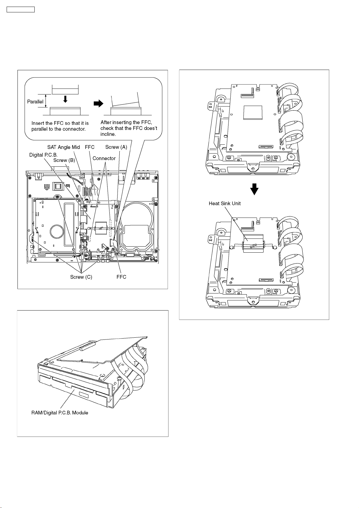
9.6. RAM/Digital P.C.B. Module
Note:
After replacing RAM/Digital P.C.B. Module, “TM AV1” is displayed
on FL.
Once power off, and start-up again.
27
Page 28
DMR-EX80SEG
1. Remove 1 Screw (A) and 1 Screw (B) to remove SAT Angle
Mid.
2. Remove 2 FFCs and 5 Screws (C).
3. Lift up Digital P.C.B. slightly so to disconnect Connectors to
remove Digital P.C.B.
Note:
RAM/Digital P.C.B. Module as service part has no heat sink
unit.
Before returning to customer, heat sink unit should be
installed on Digital P.C.B..
4. Put Digital P.C.B. on RAM Drive and remove RAM/Digital
P.C.B. Module.
28
Page 29

DMR-EX80SEG
9.7. DV Jack P.C.B.
1. Remove 1 Screw (A) to remove DV Jack P.C.B.
9.8. HDD
29
Page 30

DMR-EX80SEG
1. Remove 1 Screw (A), 1 Screw (B) and 1 Screws (C) to
remove SAT Angle R.
2. Remove ATAPI Connector and HDD Power Connector.
3. Remove 2 Screws (D) to remove HDD Angle with HDD.
9.9. Rear Panel
1. Disconnect Fan Connector.
4. Put HDD with HDD Angle up side down not to give a shock
to HDD.
5. Remove 2 Screws (A), remove HDD.
2. Remove 7 Screws (A) and 2 Screws (B).
3. Unlock 2 Locking Tabs (A) to remove Rear Panel.
30
Page 31

DMR-EX80SEG
9.9.1. Fan Motor
1. Disconnect Fan Connector and remove 2 Screws (A).
2. Push and unlock 2 Locking Tabs (A) to remove Fan Motor.
9.10. Power P.C.B.
1. Remove 1 Screw (A).
2. Remove 3 Screws (B) and disconnect Connector (A) to
remove Power P.C.B..
31
Page 32

DMR-EX80SEG
9.11. Main P.C.B. and Front (L)
P.C.B.
1. Remove 1 Screw (A).
2. Remove 3 Screws (A) and 1 Screw (B).
3. Remove Digital Angle to remove Main P.C.B. and Front (L)
P.C.B..
9.12. SAT Adapter P.C.B.
1. Pull out the SAT Adapter P.C.B. in the direction of the
arrow.
9.13. HDMI P.C.B.
1. Pull out the HDMI P.C.B. in the direction of the arrow.
32
Page 33

10 Measurements and Adjustments
10.1. Service Positions
Note:
For description of the disassembling procedure, see the section 9.
10.1.1. Checking and Repairing of Power P.C.B.
DMR-EX80SEG
33
Page 34

DMR-EX80SEG
10.1.2. Checking and Repairing of RAM / Digital P.C.B. Module
34
Page 35

10.1.3. Checking and Repairing of Main P.C.B.
DMR-EX80SEG
35
Page 36

DMR-EX80SEG
10.1.4. Checking and Repairing of HDD
36
Page 37

10.2. Caution for Replacing Parts
10.2.1. Items that should be done after replacing parts
DMR-EX80SEG
37
Page 38

DMR-EX80SEG
Note3:
Please prepare latest firmware updating disc.
* Main Firm is being recorded in HDD, but new HDD has no data.
Writing Procedure of Main Firm:
<<Caution>>
(1) Writing of Main Firm needs 3, 4 minutes.
(2) Never cut the power of DVD Recorder until writing in Firmware ends.
(3) Initial settings and contents of reservation will not change if writing is normally completed.
1. Prepare updating disc for firm ware.
2. Replace HDD.
3. Turn on power of DVD Recorder.
4. After [PLEASE WAIT] is displayed on FL., [HDD ERR] is displayed on FL.
5. Tray opens automatically.
6. Insert updating disc for Firmware and press OPEN/CLOSE key. (If a wrong disc was inserted, [NG DISK] [NO FVU] is
displayed on FL.)
7. [LOAD] ® [LD FVU] ¬® [M_FIRM] are displayed on FL alternately.
8. [MAIN] ¨ [UPD OK] blink alternately and Tray opens. Take out disc (Writing was finished).
9. Press Power button to turn off power.
10. Press Power button to turn on power.
11. [HELLO] ® [SELF CHECK] are displayed on FL.
12. [UNFORMAT] is displayed on FL.
13. After [UNFORMAT] was displayed, message to request FORMAT is displayed on TV screen.
14. Select [Yes] and press [ENTER] key to format HDD.
(After FORMAT, program in HDD will be lost, but Main firm will not be lost.
“Write of the main farm" is completed above.
* Drive firm is not updated by above operation. If you wish update Drive firm, please prepare the disc for latest firmware update,
and write it again.
* If the version of the firm you have prepared was same as or later than that has already been written in deck, ´UNSUPPORT´
is displayed on FL.
* In a usual updating of firmware, writing is not performed when the timer reservation standby was not released.
10.2.2. Notice after replacing RAM/Digital P.C.B. Module
After replacing RAM/Digital P.C.B. Module, “TM AV1” is displayed on FL.
Once power off, and start-up again.
38
Page 39

10.3. Standard Inspection Specifications after Making Repairs
After making repairs, we recommend performing the following inspection, to check normal operation.
No. Procedure Item to Check
1 Turn on the power, and confirm items pointed out. Items pointed out should reappear.
2 Insert RAM disc. The Panasonic RAM disc should be recognized.
3 Enter the EE (TU IN / AV IN - AV OUT) mode. No abnormality should be seen in the picture, sound or operation.
4 Perform auto recording and playback for one minute using the RAM
disc.
5 Model with the HDD: Perform auto recording and playback for one
minute using the HDD.
6 If a problem is caused by a VCD, DVD-R, DVD-Video, Audio-CD, or
MP3, playback the test disc.
7 Models with SD Card Slot or DV Input Jack: In case of that the
trouble is caused by SD card and/or DV terminal.
8 After checking and making repairs, upgrade the firmware to the
latest version.
9 Transfer [9][9] in the service mode setting, and initialize the service
settings (return various settings and error information to their
default values. The laser time is not included in this initialization).
Use the following checklist to establish the judgement criteria for the picture and sound.
Item Contents Check Item Contents Check
Block noise
Crosscut noise Noise (static, background noise, etc.)
Picture
Dot noise The sound level is too low.
Picture disruption The sound level is too high.
Not bright enough The sound level changes.
Too bright
Flickering color
Color fading
No abnormality should be seen in the picture, sound or operation.
*Panasonic DVD-RAM disc should be used when recording and
playback.
No abnormality should be seen in the picture, sound or operation.
No abnormality should be seen in the picture, sound or operation.
Models with SD Card or DV Input Jack;
1) SD Card: Check to be able to display and copy the picture.
2) DV terminal: Check to be able to record from DVC.
Make sure that [FIRM_SUCCESS] appears in the FL displays.
*[UNSUPPORT] display means the unit is already updated to
newest same version. Then version up is not necessary.
Make sure that [CLR] appears in the FL display.
After checking it, turn the power off.
Distorted sound
Sound
DMR-EX80SEG
39
Page 40

DMR-EX80SEG
40
Page 41

11 Block Diagram
11.1. Power Supply Block Diagram
DMR-EX80SEG
POWER P.C.B. MAIN P.C.B.
AC INLET
P1101
VA1110,L1120 D1140,C1143
F1101
SURGE
SUPPRESSOR
AND
SURGE
ABSORBER
RECTIFIER
IC1150
(SWITCHING IC)
7VIN
2
F/B 10
134
9
5
VCCGNDZ/C
T1150
POWER
SWITCHING
TRANSFORMER
P1
12
P2
V2
8
V1
7
Q1700
(REG.X SW+3.8V)
D1270
1
2
3
2
3
4
5
IP1601
21
QR1800,QR1801
SWITCHING
IC1701
(DC/DC CONVERTER)
CURRENT
1
VIN
SENSE
FET
GATE
DRIVE
PW
2
IC1601
(DC/DC CONVERTER)
1
2
ON
VIN
PW
ON
GND
CURRENT
SENSE
FET
GATE
DRIVE
GND
8
7
6
8
7
6
4
3
Q1600
(REG.X SW+5.8V)
1
2
3
4
G
FET
G
FET
1
DS
2
5
6
5
DS
6
7
8
16,17,19
3,4,5,6
P1501P1102X SW+3.8V
P1501P1102X SW+5.8V
FROM
TIMER
SECTION
DI P ON
IC7501- 44
H
Q1501,D1502
REGULATOR
IC1521
(REG.ANA+3.3V)
VOUTVIN 1
8
GND CONT
45
X SW+3.8V
X SW+3.3V
ANA+3.3V
A
B
IC7501- 16
C
D
Q1200
(FEED BACK)
4
32
1
COLDHOT
CN9006
16
TO
SAT MAIN
P.C.B.
CN9006 P1104
52
CN9006 P1104
34
CN9006 P1104
61
2
1
IC1200
(ERROR VOLTAGE DET.)
P1104
3
X SW+12V
P1102
8
12,13,14,15
P1501
P1501P1102
P ON
H
T7501
DISPLAY HEATER
POWER SWITCHING
TRANSFORMER
51
PWR SAVE :ON
IC7501- 79
DR P ON
IC7501- 42
DMR-EX80SEG
H
D7505
H
FROM
TIMER
SECTION
FROM
TIMER
SECTION
IC7504-
Q1502
(DR+12V OUT)
1
2
FET
G
3
4
IC7401
(REG.PS+11.6V)
VOUTVIN 3
1
H
:ON
GND
5
2
DS
5
6
7
8
IP1501
21
PS+11.6V 846IC3001- ,IC4009-
DR+12V
IP7501
QR7401
( :ON)
QR1501
( :ON)
21
H
H
E
15
G
H
I
J
Power Supply Block Diagram
41
Page 42

DMR-EX80SEG
POWER OFF
AU+5V
XSW+3V
ANA+3.3V
D+3.3V
A
B
C
D
E
X SW+3.8V
IC1506
(REG.DR+5V)
VOUTVIN 3
1
CONT
GND
52
IC1520
(REG.ANA+5V)
VOUTVIN 5
1
CONT
GND
23
IC4011
(REG.AU+5V)
VOUTVIN 5
4
H
:ON
GND
2
3
2IC4901-
DR+5V
ANA+5V
AU+5V
IC1504
(REG.D+5V)
V IN
1
GND CONT
5
V OUT
2
D+3.8V
ANA+5V
DR+5V
5
L
P7402 P59001
30
P7402 P59001
25
P7402 P59001
42
P7402 P59001
56
P7402 P59001
34
P7402 P59001
60,62
P7402 P59001
76
P7402 P59001
22,24
+
Vref
VOUTVCC
TO/FROM
DIGITAL
P.C.B.
FROM
TIMER
SECTION
45
32
HDMI 5V REG
IC7501- 54
HDMI 3V REG
IC7501- 34
IC7501- 40
IC1522
(HDD PFAIL OUT)
L
XSW5.8V2P7501 P56101
D+3.8V
LHDD PFAIL
P7501 P56101
4,5
P56101P7501
9
P56101P7501
10
HDMI P.C.B.MAIN P.C.B.
IC56105
(REG.+5V)
P56102-
VIN1
CONT
2
3VO
18
IC56104
(REG.+3.3V)
VIN8
1VOUT
ON
H
5
IC56103/IC56107(+3.3V)
L
IC7501-
IC7501- 73
62IC7501- / 90 99/
12
PS+11.6V
CN8001P7413
10
IC8000-
8
SAT ADAPTER P.C.B.
Q7509
IC7502
(RESET)
IC7505
(RESET)
VDD 12
VOUTVDD 45
P FAIL
OUT
X SW+5.8V
IC7507
(REG.BOOSTER+5V)
8 VIN
VOUT
GND
GND
4
VOUTVIN 1
CONT
54
1
5
CONT
IC7403
(REG.PS+5V)
G
H
I
J
8
BOOSTER+5V
PS+5V
XSW+12V
DR+12V
64,66,68,70,72,74
14,16
DR+12V
P1503
1
P1503
DR+5V
948442IC3001- / /
,
7IC7504-
,
3IR7501-
P59001P7402
P59001P7402
TO
DIGITAL
P.C.B.
TO HDD
4
402586IC3001- / / /
DMR-EX80SEG
Power Supply Block Diagram
42
Page 43

11.2. Analog Video Block Diagram
DMR-EX80SEG
FROM
DIGITAL P.C.B.
DIGITAL VIDEO
BLOCK SECTION
AV2
(DECODER/EXT)
MAIN P.C.B.
JK3901
21 PIN JACK
AV1
(TV)
AV3
JK3002
FRONT JACK
S-VIDEO IN
1
VIDEO IN
AV4
JK3001
REAR JACK
VIDEO
IN
AV4
JK3001
S-VIDEO
S-VIDEO IN
JK3901
21 PIN JACK
RED/C
GREEN
BLUE
VIDEO/Y
C OUT DM
P7402P59001
55
P59001 P7402
P59001 P7402
P5900167P7402
432
43124
15
11
7
20
Y OUT DM
51
RPROUT DM
59
GPYOUT DM
P7402P59001
63
BPBOUT DM
AV1 VIDEO
20
AV3 Y
3
AV3 C
4
AV3 V
8
7
AV4 V
14
15
Y
AV4 Y
3
C
AV4 C
AV2 R/C
AV2 G
AV2 B
AV2 V/Y
IC3001
(VIDEO PROCESSOR)
91
93
95
97
99
33
41
45
37
35
39
43
1
3
5
31
AV1 V
AV3 Y
AV3 C
AV3 V
AV4 V
AV4 Y
AV4 C
AV2 R/C
AV2 G
AV2 B
AV2 V/Y
CLAMP/
BIAS
CLAMP/
BIAS
BIAS
CLAMP
CLAMP
CLAMP
CLAMP
BIAS
CLAMP
CLAMP
CLAMP
BIAS
BIAS
CLAMP
CLAMP
CLAMP
CLAMP
6MHz
BPF
6MHz
LPF
(SW10)
b
a
:PB SIGNAL:REC SIGNAL
(SW2)
a
b
c
(SW3)
a
b
c
d
(SW6)
a
b
c
d
SV1
a
b
c
d
e
SV2
a
b
c
d
e
IIC BUS
LOGIC
CLAMP
COMP
R-Y
OUT
AV1
R-C
OUT
COMP
B-Y
OUT
AV1
B
OUT
COMP
Y
OUT
AV1
G
OUT
AV4
Y
OUT
AV4
C
OUT
AV4
V
OUT
AV1
V/Y/C
OUT
AV2
V
OUT
C-ADC
OUT
V/Y
ADC
OUT
SLICER
SCL
SDA
DT C IN
DT Y IN
TUNER
V
7
9
11
12
14
15
17
20
19
22
23
24
26
28
81
83
85
88
89
48
47
OPEN
30
SLICER
IIC CLK
IIC DATA
IC7501- 26
2.3V
BQ7501,Q7503-
FROM/TO
TIMER
SECTION
25IC7501-
5V
1.0V
CPN CIN DM
V/Y IN DM
< R >
< G >
< B >
< RGB CPSV >
G DTC IN A
G DTY IN A
AV1 V
AV3 Y
AV3 C
AV3 V
AV4 V
AV4 Y
AV4 C
AV2 R/C
AV2 V/Y
TUNER V
(SW1)
a
b
c
(SW4)
a
b
c
(SW5)
a
b
c
(SW7)
a
b
(SW8)
a
b
(SW9)
a
b
ADC
OUTPUT
SELECT
SWITCH
CIRCUIT
6MHz
12MHz
+
6MHz
12MHz
6MHz
12MHz
JK3903
2
1
4
3
6
5
JK3801
21PIN JACK
JK3001
S-VIDEO
Y
9
C
10
JK3001
VIDEO OUT
13
15
JK3901
21PIN JACK
P7402 P59001
75
71
P7402 P59001
88
83
P7402 P59001
87
84
P7412 CN8000
6
8
P59001P7402
P59001P7402
P59001P7402
CN8000P7412
PR
PB
Y
RED/C15
BLUE7
GREEN11
VIDEO/Y19
VIDEO19
TO
DIGITAL P.C.B.
DIGITAL VIDEO
BLOCK SECTION
CN8002 CN9007
2419
AV1
(TV)
AV2
(DECODER/EXT)
17
CN9007CN8002
COMPONENT
VIDEO OUT
PROGRESSIVE/
INTERLACE
AV4
AV4
FROM
SAT MAIN P.C.B.
DIGITAL VIDEO
BLOCK SECTION
< B >
< RGB CPSV >
< G >
< R >
DMR-EX80SEG
Analog Video Block Diagram
43
Page 44

DMR-EX80SEG
11.3. Analog Audio Block Diagram
AV3
AV4
(REAR)
FROM
MAIN P.C.B.
FROM
TIMER
SECTION
FROM
DIGITAL
P.C.B.
DIGITAL AUDIO
BLOCK SECTION
JK3002
FRONT INPUT JACK
JK3001
REAR INPUT JACK
AUDIO
AUDIO
P.C.B.DIGITAL
LINE
(Lch/MONO)
XTMUTE
IC7501-
XDMUTE
IC54402-
(DECODER/EXT)
LINE
(Rch)
LINE
(Rch)
LINE
(Lch)
65
16
P7402P59001
41
P59001 P7402
39
JK3901
21 PIN JACK
AV1
(TV)
AV2
IC8000
(BUFFER)
MIX R OUT DM
MIX L OUT DM
AUDIO IN ch2(R)
2
AUDIO IN ch1(L)
6
AUDIO IN ch2(R)
2
AUDIO IN ch1(L)
6
13
12
11
10
9
20
21
17
18
Q4060,QR4002
MUTE
CIRCUIT
D4005
Q4006
MUTE
Q4007
MUTE
D4006 Q4009
MUTE
Q4008
MUTE
IC4009
(BUFFER)
12
67
IC3001
(AUDIO SIGNAL PROCESSOR)
DAC Rch
56
DAC Lch
64
AV1 Rch
52
AV1 Lch
60
AV2 Rch
53
AV2 Lch
61
AV3 Rch
50
AV3 Lch(FRONT)
58
AV4 Rch
51
AV4 Lch
59
DT Lch
63
DT Rch
55
(SA5R)
AV4
TUN
(SA5L)
AV4
TUN
BUFF.
BUFF.
(SA1R)
a
b
c
d
e
(SA3R)
a
b
c
d
e
(SA2R)
a
b
c
d
e
(SA2L)
a
b
c
d
e
(SA3L)
a
b
c
d
e
(SA1L)
a
b
c
d
e
OUTPUT
SELECT SWITCH
(SA4R)
a
b
c
d
OUTPUT
SELECT SWITCH
(SA4L)
a
b
c
d
LPF
AGC
LPF
LPF
AGC
LPF
BUFF.
BUFF.
BUFF.
BUFF.
MUTE
ADC Rch
AMP
MUTE
MUTE
ADC Lch
AMP
MUTE
AV1 Rch
ADC Rch
AV2 Rch
AV2 Lch
ADC Lch
AV1 Lch
:PB SIGNAL:REC SIGNAL
JK3001
REAR JACK
MIX L OUT2
MIX R OUT2
72
79
74
73
78
71
AUDIO OUT Ch2(R)
AUDIO OUT Ch1(L)
AUDIO OUT Ch2(R)
AUDIO OUT Ch1(L)
AADC R
AADC L
16
18
19
21
JK3901
21 PIN JACK
1
3
1
3
P740219P59001
P7402 P59001
LINE OUT
(L)
LINE OUT
(R)
AV1
(TV)
AV2
(DECEODER/EXT)
17
TO
P.C.B.DIGITAL
DIGITAL AUDIO
BLOCK SECTION
AV4
FROM
SAT
MAIN P.C.B.
CN8002
CN9007
6
CN9007 CN8001
14157
CN8002CN9007
9
CN9007 CN8001
111210
LP
LM
RP
RM
STA ADAPTER P.C.B.
FROM
P59001 P7402
DIGITAL
P.C.B.
44
IEC OUT
CN8000
P7412
12
CN8000 P7412
10
G DT IN L A
G DT IN R A
OPEN
OPEN
54
62
TUN Rch
TUN Lch
44
IIC BUS
LOGIC
SCL
SDA
88
89
5V
2.3V
1.0V
IIC CLK
25
IC7501-
IIC DATA
26
IC7501-
IC4901
OPTICAL
(DIGITAL AUDIO OUT)
1
FROM
TIMER
SECTION
DMR-EX80SEG
Analog Audio Block Diagram
Page 45

11.4. Analog Timer Block Diagram
DMR-EX80SEG
IR7501
REMOTE CONTROL
RECEIVER
IC7505
(RESET)
S7506
STOP
S7505
SELECT
IC7501
(TIMER)
MAIN P.C.B.
CTL.GNDVDD
132
OUTBOOSTER+5V 2
1VDD
S7500
EXT LINK
S7508
REC
S7507
PLAY
S7504
OPEN/CLOSE
S7501
CH-DOWN
S7503
CH-UP
IR
KEY IN1
KEY IN2
KEY IN3
REMOTE CTL.
3
SYS PFAIL
74
PFAIL
73
KEY IN1
86
KEY IN2
87
88
KEY IN3
H
L
POWER SAVE 61
H
RESET
L
12
FL TXD 5
FL RXD
6
FL CLK
L
FL RESET 51 RESET8
FL CS 45 CS3
IIC DATA
IIC CLK
26
25
IIC DATA
IIC CLK
X SW+3.8V
H
P SAVE
QR7508
( :ON)
H
Q7510
( :OFF)
IC7502
(RESET)
VDD
45
QR7504
QR7503
X SW+12.4V
L
BOOSTER +5V
IIC DATA
IC3001-
IIC CLK
IC3001-
89
88
IP7501
(IC PROTECTOR)
21
TO
ANALOG
VIDEO/
ANALOG
AUDIO
SECTION
T7501
DISPLAY HEATER
POWER SWITCHING
TRANSFORMER
HEATER+
9
+B
1
3
8
HEATER-
IC7504
(DISPLAY DRIVE)
VCC7
S DATA10
SCK
97
GND4
+38V
GND
-33V
FL29
FL28
FL26
FL24
FL21
FL20
FL18
FL17
FL15
FL14
FL12
FL11
FL10
FL06
FL05
FL04
FL03
FL01
FL00
FL25
FL22
FL16
FL13
FL09
FL07
FL02
FL30
7
6
D7505
5
DP7501
45
F-F+1
15
VP
12
13
16
18
21
22
24
25
27
28
30
31
32
36
37
38
39
1
2
17
20
26
29
33
35
40
11
Q7514
FL DRIVE
41
41
38
36
33
32
30
29
27
26
24
23
22
18
15
13
11
9
7
37
34
28
25
21
19
10
42
8
P1/P1
P/P2
NC/P3
P6/P6
PL21
P7/P7
P8/P8
P9/P9
P10/P10
P11/P11
NC/P12
P12/P13
4G/P14
5G/P16
6G/NX
P13
P14
P15
P16
P3/1G
P5/2G
2G/4G
3G/5G
NC/6G
NC7G
7G
1GA1G
1GB
TIMER
DISPLAY
S7002
POWER
FRONT(L) P.C.B.
SAT MAIN P.C.B.
HDMI P.C.B.
CN9007
7
CN9007
6
CN9007
5
CN8002
14
CN8002
15
CN8002
16
10
X7502
32.768KHz
FC7001FC7000
1
X7501
10MHz
P7413CN8002
1
P7413CN8002
2
P7413CN8002
3
P7501P56101
7
P7501P56101
6
XCIN
11
XCOUT
13
XOUT
15
XIN
28
DIG S CLK
29
DIG S IN
30
DIG S OUT
27
DIG S CS
20
HDMI-CEC-IN
78
HDMI-CEC-OUT
XTMUTE
SYNC IN
CVIN1
DR POWER ON
DI POWER ON
TU POWER ON
TBUS CLK3537
TBUS TXD
TBUS RXD
FAN PWM OUT 22
FAN LOCK H 39
65
98
89
42
H
H
44
H
43
36
Q7503
BUFFER
Q7501
BUFFER
G SCLK A
G SBPTM A
G SBMTP A
X SW+12.4V
Q7511
Q7505
XT MUTE
QR4002-
B
SLICER VIDEO
IC3001-
85
H
DR P ON
B
QR1501-
H
DI P ON
5
IC1521- , etc.
H
TU P ON
5
IC7801-
SCLK
P7402-
3
SBPTM
P7402-
7
SBMTP
P7402-
9
P1501
P1501
TO/FROM
ANALOG A/V SECTION
TO
POWER SUPPLY SECTION
TO
TUNER P.C.B.
TO/FROM
DIGITAL P.C.B.
P1103
P1103
FAN MOTOR
M
1
3
DMR-EX80SEG
Timer Block Diagram
P1102
23
23
P1102
23
23
45
Page 46

DMR-EX80SEG
11.5. HDMI Block Diagram
FROM/TO
DIGITAL
BLOCK SECTION
11
12
25
27
29
31
39
IC56103IC56101
IC56102
FP56101P55002
2
39
FP56101P55002
3
38
FP56101P55002
5
36
FP56101P55002
6
35
FP56101P55002
8
33
FP56101P55002
9
32
FP56101P55002
30
FP56101P55002
29
Line Driver
FP56101P55002
16
FP56101P55002
14
FP56101P55002
12
FP56101P55002
10
FP56101P55002
2
(HDMI TRANSMITTER)
D0
161
D1
160
D2
159
D3
158
D4
156
D5
155
D6
154
D7
153
AMSDI0
2
AMSDI1
3
AMSDI2
4
AMSDI3
5
AMRX
7
TX2P
TX2M
TX1P
TX1M
TX0P
TX0M
TXCP
TXCM
81
L56101
80
77
L56102
76
73
L56103
72
69
L56104
68
Q56105
SWITCHING
Q56104
VIDEO EE SIGNAL
VIDEO PB SIGNAL
AUDIO EE SIGNAL
AUDIO PB SIGNAL
HDMI
CONNECTOR
P56102
P56102
P56102
P56102
P56102
P56102
P56102
P56102
P56102
10
12
13
D2+
1
D2-
3
D1+
4
D1-
6
D0+
7
D0-
9
CLK+
CLK-
CEC
FP56101P55002
22
FP56101P55002
201921
15
14
HSDA
HSCL
46
SCL
SDA
46
45
Q56103
3V-5V
Conv.
Q56102
3V-5V
Conv.
Q56001,2
BUFFER
P56102
15
P56102
16
HDMI SDA
HDMI SCL
P561016P7501
6
P561017P7501
7
DMR-EX80SEG
HDMI Block Diagram
HDMI-CONT
HDMI-MONI
Page 47

12 Schematic Diagram
12.1. Interconnection Schematic Diagram
DMR-EX80SEG
FC7000
KEY3_POWER
1
2
FRONT(L) P.C.B.
G
F
E
P1101
A
N
P1104
P_ON_H
X_SW3R8V
GND
X_SW5R8V
GND
X_SW12V
P1102
X_SW5R8V 3
X_SW5R8V
X_SW5R8V
X_SW5R8V
GND
GND
GND
GND
GND
X_SW12V
X_SW12V
X_SW12V
X_SW12V
X_SW3R8V
X_SW3R8V
P_ON_H
D3R8V
P_SAVE_L
FANLOCK
FAN_GND
FANOUT
P1103
FANOUT
FAN_GND
FANLOCK
1
2
3
4
5
6
1
2
4
5
6
7
8
9
10
11
12
13
14
15
16
17
18
19
20
21
22
23
1
2
3
POWER P.C.B.
FAN MOTOR
D
DR12V
DR_GND
DR_GND
DR5V
GND
CS1CS0DA2
DA0
C
B
A
DA1
INTRQ
GND
DMACKCSEL
IORDY
GND
DIORGND
DIOWGND
DMARQ
GND
DD15
DD0
DD14
DD1
DD13
DD2
DD12
DD3
DD11
DD4
DD10
DD5
DD9
DD6
DD8
DD7
GND
RESET-
HDD
1
2
3
4
1
2
3
4
5
6
7
8
9
10
11
12
13
14
15
16
17
18
19
20
21
22
23
24
25
26
27
28
29
30
31
32
33
34
35
36
37
38
39
40
FC7001
KEY3_POWER1
2
GNDGND
P1501
1
2
3 X_SW5R8V
X_SW5R8V
4
X_SW5R8V
5
6
X_SW5R8V
GND
7
GND
8
GND
9
GND
10
GND
11
X_SW12V
12
X_SW12V
13
X_SW12V
14
X_SW12V
15
X_SW3R8V
16
X_SW3R8V
17
P_ON_H
18
X_SW3R8V
19
P_SAVE_L
20
FANLOCK
21
FAN_GND
22
FANOUT
23
P1503
DR12V
1
DR_GND
2
DR_GND
3
DR5V
4
P7412 CN8000
DEC AUD L 12 12 AUDIO L
AGND
DEC AUD R
AGND
DEC Y OUT
AGND
DEC C OUT
AGND
GND
PS11R6V
GND
ASCO TXD
ASCO RXD
T CS
T DATA
T CLK
P.C.B Name
Main
P.C.B.
P7413
11
10
9
8
7
6
5
4
3
2
1
11
10
9
8
7
6
5
4
3
2
1
Circuit Name
Main Net
A/V I/O
Timer
MAIN P.C.B.
CN8002
1 GNDA
Y1
32GNDA
4
C1
5
GNDA
6
LP
7
LM
8
GNDA
9
RP
10
RM
GNDA
11
12
GNDA
13 GND
T-CLK
1514T-DATA
16
T-CS
17
GND
18
RXD
19
TXD
20
GND
AUDIO GND
1011AUDIO R
9
GNDA
8
Y1
7
GNDA
6
C1
5
4
GNDA
3
2
1
CN8001
GND
1011AUDIO 12V
9
GND
8
7
6
5
TX
4
RX
3
T CS
2
T DATA
1
T CLK
SAT ADAPTER P.C.B.
Ref.No.
Ref.No.1500,7400 SERIES
Ref.No.3000,3900,4000,4900 SERIES
Ref.No.7500 SERIES
DGND
DGND
DGND
DGND
DGND
DGND
DGND
DGND
DGND
DGND
DGND
DGND
XINTP
DR12V
SCLK
DR12V
XINTM
DRGND
SBPTM
DRGND
SBMTP
DR5V
XMPREQ
DR5V
AU5V
ITM2A
XDMUTE
ITA2M
AADC_L
P_OFF_L2
AADC_R
XFWE
AUGND
D3R3V
AUGND
I2C5DT
AUGND
I2C5CK
MIXLOUT_DM
IT_CK
MIXROUT_DM
X_SW_3R2V/D3R3V
DGND
IECOUT
DGND
DGND
DGND
UARTP2M
DGND
UARTM2P
YOUT_DM
P_OFF_L3
DGND
CSYNC_IN
COUT_DM
ANA3R3V
DGND
EPG_ON_H/BUSY
RPROUT_DM
X_SW3R8V
DGND
X_SW3R8V
GPYOUT_DM
X_SW_12V
DGND
X_SW_12V
BPBOUT_DM
X_SW_12V
DGND
X_SW_12V
V_YIN_DM
X_SW_12V
DGND
X_SW_12V
CPNCIN_DM
ANA5V
DGND
DGND
BS_ON
EPG_VIDEO
DGND
DGND
G_IN
RGB_CPSVIN
DGND
DGND
B_IN
R_IN
P7501
GND
X SW 5.8V
GND
X SW 3.8V
X SW 3.8V
HDMI CONT
HDMI MONI
HOT PLUG
HDMI P5 ON H
HDMI P3 ON H
P59001P7402
DGND
1
2
3
4
5
6
7
8
9
10
11
12
13
14
15
16
17
18
19
20
21
22
23
24
25
26
27
28
29
30
31
32
33
34
35
36
37
38
39
40
41
42
43
44
45
46
47
48
49
50
51
52
53
54
55
56
57
58
59
60
61
62
63
64
65
66
67
68
69
70
71
72
73
74
75
76
77
78
79
80
81
82
83
84
85
86
87
88
1
2
3
4
5
6
7
8
9
10
1
DGND
2
DGND
3
DGND
4
DGND
5
DGND
6
DGND
7
DGND
8
DGND
9
DGND
10
DGND
11
DGND
12
XINTP
13
DR12V
14
SCLK
15
DR12V
16
XINTM
17
DRGND
18
SBPTM
19
DRGND
20
SBMTP
21
DR5V
22
XMPREQ
23
DR5V
24
AU5V
25
ITM2A
26
XDMUTE
27
ITA2M
28
AADC_L
29
P_OFF_L2
30
AADC_R
31
XFWE
32
AUGND
33
D3R3V
34
AUGND
35
I2C5DT
36
AUGND
37
I2C5CK
38
MIXLOUT_DM
39
IT_CK
40
MIXROUT_DM41
X_SW_3R2V/D3R3V
42
DGND
43
IECOUT
44
DGND
45
DGND
46
DGND
47
UARTP2M
48
DGND
49
UARTM2P
50
YOUT_DM
51
P_OFF_L3
52
DGND
53
CSYNC_IN
54
COUT_DM
55
ANA3R3V
56
DGND
57
EPG_ON_H/BUSY
58
RPROUT_DM
59
D3R8V
60
DGND
61
D3R8V
62
GPYOUT_DM
63
D1R2V
64
DGND
65
D1R2V
66
BPBOUT_DM
67
D1R2V
68
DGND
69
D1R2V
70
V_YIN_DM
71
D1R2V
72
DGND
73
D1R2V
74
CPNCIN_DM
75
ANA5V
76
DGND
77
DGND
78
BS_ON
79
EPG_VIDEO
80
DGND
81
DGND
82
G_IN
83
RGB_CPSVIN
84
DGND
85
DGND
86
B_IN
87
R_IN
88
GND
IECOUT
GND
DAC MCK
GND
DAC BCK
GND
DAC LRCK
GND
ADACOUT0
GND
ADACOUT1
GND
ADACOUT2
GND
DMIX
GND
RESET
GND
HDMI 2 IRQ
I2C SCL1
I2C SDA1
HDMI 1 IRQ
GND
HDMI 27CLK
GND
R656 CLK
GND
R656 OUT7
R656 OUT6
GND
R656 OUT5
R656 OUT4
GND
R656 OUT3
R656 OUT2
GND
R656 OUT1
R656 OUT0
GND
TPA+
TPANC
NC
TPB+
TPB-
CN9007
1
2
3
4
7
8
9
10
11
12
13
14
15
16
17
18
20
GNDA
Y1
GNDA
C1
GNDA
LP56
LM
GNDA
RP
RM
GNDA
GNDA
GND
T-CLK
T-DATA
T-CS
GND
RXD
TXD19
GND
P55002
SAT MAIN P.C.B.
TU9000
TUNER
PACK
P_ON_H
X_SW3R8V
GND
X_SW5R8V
GND
X_SW12V
CN9006
6
5
4
3
2
1
DIGITAL P.C.B.
Ref.No.
Ref.No.50000 SERIES
Ref.No.50000,53000,54000,
55000,57000 SERIES
Ref.No.54000 SERIES
Ref.No.59000 SERIES
Ref.No.59000 SERIESModel Select
P56101
GND
X SW 5.8V
GND
X SW 3.8V
X SW 3.8V
HDMI CONT
HDMI MONI
HOT PLUG
HDMI P5 ON H
HDMI P3 ON H
1
2
3
4
5
6
7
8
9
10
HDMI P.C.B.
P58001
1
2
3
4
5
6
7
8
9
10
11
12
13
14
15
16
17
18
19
20
21
22
23
24
25
26
27
28
29
30
31
32
33
34
35
36
37
38
39
40
GND
CS1CS0DA2
DA0
DA1
INTRQ
GND
DMACKCSEL
IORDY
GND
DIORGND
DIOWGND
DMARQ
GND
DD15
DD0
DD14
DD1
DD13
DD2
DD12
DD3
DD11
DD4
DD10
DD5
DD9
DD6
DD8
DD7
GND
RESET-
Digital
P.C.B.
Circuit Name
FEP
BE
Audio I/O
D Net/EPG
P.C.B Name
40
39
38
37
36
35
34
33
32
31
30
29
28
27
26
25
24
23
22
21
20
19
18
17
16
15
14
13
12
11
10
9
8
7
6
5
4
3
2
1
1
2
3
4
5
6
FP56101
1
2
3
4
5
6
7
8
9
10
11
12
13
14
15
16
17
18
19
20
21
22
23
24
25
26
27
28
29
30
31
32
33
34
35
36
37
38
39
40
P37001PS57001
1
2
3
4
5
6
GND
IECOUT
GND
DAC MCK
GND
DAC BCK
GND
DAC LRCK
GND
ADACOUT0
GND
ADACOUT1
GND
ADACOUT2
GND
DMIX
GND
RESET
GND
HDMI 2 IRQ
I2C SCL1
I2C SDA1
HDMI 1 IRQ
GND
HDMI 27CLK
GND
R656 CLK
GND
R656 OUT7
R656 OUT6
GND
R656 OUT5
R656 OUT4
GND
R656 OUT3
R656 OUT2
GND
R656 OUT1
R656 OUT0
GND
TPA+
TPANC
NC
TPB+
TPB-
DV JACK P.C.B.
P50001
LDD VCC121
LDD VCC1
LDD VSS
LDD VSS
LDD ENABLE
LDD GND2
LDD IINRD
LDD IINW1
LDD IINW2
LDD IINW3
SC/ROHM
LDD W1
LDD W1N
LDD W2
LDD W2N
LDD W3
LDD WN
LDU HFM
LDU HFMN
LDU CD/DVD
OEIC GND
OEIC VC
FM VOUTFM VOUT+
FM/OEIC VCC:5V
OEIC D
OEIC C
OEIC RF+
OEIC RFOEIC B
OEIC A
OEIC EI
OEIC FJ
OEIC GK
OEIC HL
OEIC SW2
OEIC SW1
SMOUT
GND
ACT FOC2ACT FOC2+ 41
ACT TRK+
ACT TRKACT FOC1+
ACT FOC1-
FP50002
GND
GND
AA+
B+
B-
FP50003
HHWHW+
HVHV+
HUHU+
H+
COILU
COILV
COILW
FP50004
LM+
LMOPEN_SW
PHOTO_LED
CARTRIGE
REC INH
GND
CLOSE SW
P53501
CD
DAT1
DAT0
GND
CLK
WP
CMD
DAT3
DAT2
3R3V
3R3V
TPA+
TPAGND
TPB+
TPBGND
DIAG
SBI0
SBO0
3
4
5
6
7
8
9
10
11
12
13
14
15
16
17
18
19
20
21
22
23
24
25
26
27
28
29
30
31
32
33
34
35
36
37
38
39
40
42
43
44
45
1
2
3
4
5
6
1
2
3
4
5
6
7
8
9
10
11
1
2
3
4
5
6
7
8
1
2
3
4
5
6
7
8
9
10
11
12
13
14
15
16
17
18
19
20
DVD RAM DRIVE
P6802
CD
20
19
DAT1
DAT0
18
GND
17
CLK
16
WP
15
CMD
14
DAT3
13
DAT2
12
11
D3R3V
10
D3R3V
9
8
7
GND
6
5
4
GND
3
2
1
SD CARD P.C.B.
DMR-EX80SEG
Interconnection
Schematic Diagram
4321
5
6
1110987
47
Page 48

DMR-EX80SEG
12.2. Power Supply Schematic Diagram
G
F
E
D
C
IC1150
SWITCHING IC
IC-DETAIL BLOCK DIAGRAM
B
Z/C
1
FB
2
A
K2AA2H000007
LATCH RELEASE/
OVER VOLTAGE
PROTECTOR/
OVER HEATING
PROTECTOR
ZERO CURRENT
DET./ONDEADTIMER
STANDBY
CIRCUIT
ON WIDTH
TIMER
P1101
A
N
GND
ZA1103
EYF52BCY
#K3GE1ZA00010
or
SERVICE MANUAL
VCC(START)
/VCC(STOP)
3
ZA1104
EYF52BCY
or
#K3GE1ZA00010
F1101
K5D202BK0005
250V T2AL
SEE THE
+
-
CONTROL
CIRCUIT
OCP THRESHOLD
COMPARATOR/
BURST MODE
OCP THRESHOLD
COMPARATOR
VA1110
321
321
321
K1129
VWJ0795=5
C1120
#ERZVA5V471
D4EA7471A007
ECQU2A683MLC
or
ZA1105
K9ZZ00001279
ZA1106
K9ZZ00001279
ZA1107
K9ZZ00001279
UVLOUVLO
+
-
VCC(STARTUP OFF)
/VCC(STARTUP ON)
IDP(LIMIIT/
BURST)SENS.
SOFT-DRIVE
CIRCUIT
7
VIN DRAIN
START-UP
CIRCUIT
RESTERT
TIMER
L1120
G0B233D00001
1
ZA1150
1
VSC5603
ZA1151
XYN3+J8FJ
SOURCE
/OCL
LB1122
VWJ0795=5
D1140
B0EDKT000009
10K[22]
R1155
R1156
R1152
7500[G][22]16K[G][22]
(S1WBA80-7062)
43
or
R1151 6800[22]
D1156
MA2C165001VT
330P[22]C1152
12
R1153
18[22]
18[22]
C1150
F2A1V6800002
EEUFM1V680B
C1153
2200P[22]
ECJGVB1H222K
C1143
F2B2W4700003
LB1123
VWJ0795=5
D1151R1150
B0HAGM000006
35V68[JG]
MAZ4100NMF
R1157
510
[G][22]
D1152
R1154
9100
[G][22]
2
34
ECQU2A223MLC
C1122
ECKWNA102MEV
C0DACZH00017
13 95
C1123
ECKWNA102MEV
472
IC1150
B0HADV000001
ERX2SJR22E
0.22[2W]
D1157
R1158
LB1126
ERJ6GEY0R00V
C1151
F1B3D102A011
1000P[2KV]
C1154
D1155
MAZ73000BC
2341
[22]
1000P[22]
ECJGVB1H102K
L1121
G0B233D00001
C1121
HOT COLD
9
VCC
4
IC1601, IC1701
SWITCHING IC
IC-DETAIL BLOCK DIAGRAM
8
LEVEL
SHIFT
7
CONTROL LOGIC
V5
UVLOcomp
+
-
VREF
5
6
CNT.
COMP
0.8V
RESET
+-+-
P1
PU
1110 12
P2
NC
V2
879
V1
#B3PBA0000402
431
5
FBGNDEXTCS
-+
CCVREF/SSV5/PWONVIN
4321
C1125
ECKWNA102MEV
T1150
ETS28BF1W6AD
Q1200
2
25V220[JF]F2A1E2210050
EEUFM1E221B
or
C1701
NC
231
645
NC
C1702 0.1[18]
C1704 0.1[18]
C1703 0.1[18]
R1209
1K[22]
IC1200
#C0DAEMB00003
or
C0DAEJC00006
C1705
180P[18]
R1702
51K[18]
ZA1270
VSC5614
ZA1271
XYN3+J8FJ
LB1124
VWJ0795=5
R1208
2200[22]
R1210
1K[22]
0.1[22]
AR
C
32
1
Q1700
B1DHDD000022
12
DD
DD
3
SG
R1701
D1BFR0240001
24M[36]
1
243
IC1701
C0DBAZZ00132
(AL1014)
B0JBSG000010
C1200
R1205
220K[22]
56
4
8
675
C1706
D1270
0.01[18]
312
C1270
16V1800[JG]
F2A1C1820005
R1206
[18]
LB1700
J0JHC0000048
D1701
B0JCPD000021
L1400
C1201
2400[G][22]
L1701
G0A220ZA0041
R1704
12K[D][18]
R1705
5600[D][18]
G0A100HA0023
G0A100H00025
C1271
16V1800[JG]
F2A1C1820005
R1207
10K[22]
0.047[22]
ECJ2VB1E473K
R1703
ERJ3GEY0R00V
L1270
C1707
6V680[JG]
F2A0J6810007
C1272
16V820[JG]
F2A1C8210008
R1200
R1201
1200[G][22]
8200[G][22]
R1800
470[22]
D1800
MA2J11100L
100K[22]R1801
R1803
10K[22]
180P[22]
R1602
51K[22]
C1605
Q1600
B1DHED000008
(UPA1717G-E1-A)
1
243
R1601
D1BFR0240001
24M[36]
1
243
IC1601
C0DBAZZ00132
(AL1014)
8
675
8
675
C1606
0.01[22]
ECJGVB1H103K
L1601
G0A150ZA0041
[22]
LB1600
J0JHC0000048
D1601
B0JCPD000021
R1603
2000[D][22]
R1604
8200[D][22]2700[D][22]
R1605
C1607
10V680[JG]
F2A1A6810022
C1608 0.1[22]
QR1800
25V47[JF]
UNR211300L
F2A1E4700048C1800
QR1801
R1802
UNR221300L
4700[22]
2
IP1601
K5H3022A0013
P
1
25V220[JF]
F2A1E2210050
EEUFM1E221B
or
C1602 0.1[22]
C1601
C1603 0.1[22]
C1604 0.47[22]
NOTE:DO NOT USE THE PART NUMBER SHOWN ON THIS DRAWING FOR ORDERRING.
THE CORRECT PART NUMBER IS SHOWN IN THE PARTS LIST,AND MAY BE
SLIGHTLYDIFFERNT OR AMENDED SINCE THIS DRAWING WAS PREPARED.
IMPORTANT SAFETY NOTICE:
COMPONENTS IDENTIFIED WITH THE MARK HAVE THE SPECIAL CHARACTERISTICS FOR SAFETY.
WHEN REPLACING ANY OF THESE COMPONENTS.ONLY THE SAME TYPE.
TO P1501
MAIN P.C.B.
(MAIN NET SECTION)
P1102
K1KB23A00004
1
NC
2
X_SW5R8VT
3
X_SW5R8V
4
X_SW5R8V
5
X_SW5R8V
6
X_SW5R8V
7
GND
8
GND
GND
9
GND
10
GND
11
X_SW12V
12
13
X_SW12V
14
X_SW12V
15
X_SW12V
16
X_SW3R8V
17
X_SW3R8V
18
P_ON_H
19
D3R8V
20
P_SAVE_L
21
FANLOCK
FAN_GND
22
FANOUT
23
TO FAN MOTOR
P1103
K1KA03AA0192
1
FANOUT
2
FAN_GND
FANLOCK
3
TO CN9006
SAT MAIN P.C.B.
(SAT CPU SECTION)
P1104
K1KA06AA0301
1
P_ON_H
2
X_SW3R8V
GND
3
4
X_SW5R8V
5
GND
X_SW12V
6
DMR-EX80SEG
Power Supply Schematic Diagram
54321
89 1076
48
Page 49

12.3. Main Net (1/4) Section (Main P.C.B. (1/3)) Schematic Diagram (M)
NOTE:DO NOT USE THE PART NUMBER SHOWN ON THIS DRAWING FOR ORDERRING.
THE CORRECT PART NUMBER IS SHOWN IN THE PARTS LIST,AND MAY BE
SLIGHTLYDIFFERNT OR AMENDED SINCE THIS DRAWING WAS PREPARED.
N
IMPORTANT SAFETY NOTICE:
COMPONENTS IDENTIFIED WITH THE MARK HAVE THE SPECIAL CHARACTERISTICS FOR SAFETY.
WHEN REPLACING ANY OF THESE COMPONENTS.ONLY THE SAME TYPE.
DMR-EX80SEG
A
LOCATION MAP
1/4 2/4
3/4 4/4
M:Main Net Section (Page: )
M
IC7507
C0CBCDD00025
(MM1685AFBE)
5
GND
ON(H)
CN
NC
6
7
NC
NC
VO
VIN
8
4
3
2
1
1
2
AV:AV I/O Section (Page: )
T:Timer Section (Page: )
A
B
C
BOOSTER 5V
L
0.01
10V1[KB]
C154 0
C1538 10V1[KB]
IC1504
C0CBCYG00004
(PQ200WNA 1ZPH)
VIN
VO3VADJ
VC
1
2
K
X_SW_3R3V
Q1501
C1522
R1501
0.01
X_SW_3R3V
T
T
X_SW_3R8V
P
LB1503
J
TO P1102
POWER P.C.B.
P1501
K1KA23A00003
X_SW15R5V
1
X_SW5R8VT
2
3
X_SW5R8V
4
X_SW5R8V
5
X_SW5R8V
6
X_SW5R8V
7
GND
8
GND
9
GND
10
GND
11
GND
12
X_SW12V
13
T
T
T
P_G ND
FANLOCK
FANO UT
X_SW12V
X_SW12V
X_SW12V
X_SW3R8V
X_SW3R8V
P_ON_H
X_SW3R8V
P_SAVE_L
FANLOCK
FAN_GND
FANOUT
14
15
16
17
18
19
20
21
22
23
I
J0JKB0000003
LB1502
J0JKB0000003
A B C D E F G
IP1501
K5H302100004
12
LB1504
J0JKB0000003
P_GND
LB1506
J0JKB0000003
25V100[JF]
C1503
10V220[JF]
C1518
6V680
C1504
R1503
0
330
10V2R2[KB][ 22]
LB1509
J0JCC0000060
C1508 10V1[KB]
2SD1819A0L
D1502
MAZ40390HF
C152 6
IC1520
C0CBCDC00052
(S-815A50AMC-I3JTFG)
45
VO
NC
CNTGNDVIN
123
C1510 10V1[KB]
ANA5V
10V47[3F]
C151 5
IC1521
C0CBCBD0004 8
(MM1683DFBE)
5
6
7
8
C1511 10V1[KB]
C1506 10V47[3F]
GND
ON(H)
NC
NC
VIN
ANA3R3V
CN
NC
VO
C153 9
D5V
GND
5
4
R1508
0
R1507
1800[D]
R1506
2K[D]
4
3
2
1
C1512 10V1[KB]
C1509 0.01
DDGND
3
4
5
6
7
TO
MAIN NET SECTION
(3/4)
H
DMR-EX80SEG
Main Net (1/4) Section (Main P.C.B. (1/3))
Schematic Diagram (M)
54321
89 1076
49
Page 50

DMR-EX80SEG
12.4. Main Net (2/4) Section (Main P.C.B. (1/3)) Schematic Diagram (M)
A
LOCATION MAP
NOTE:DO NOT USE THE PART NUMBER SHOWN ON THIS DRAWING FOR ORDERRING.
THE CORRECT PART NUMBER IS SHOWN IN THE PARTS LIST,AND MAY BE
SLIGHTLYDIFFERNT OR AMENDED SINCE THIS DRAWING WAS PREPARED.
1/4 2/4
3/4 4/4
T
DGND T
X_SW_12R4V
1
2
3
AV
D3R3V
T
X_SW_5R8V
QR7401
UNR52130 0L
T
IO PWR_SAVE_H
AV
PS_5V
AV
BOOSTER+5VT
AV
GND
ZJ7404
K9ZZ00001279
M:Main Net Section (Page: )
AV:AV I/O Section (Page: )
T:Timer Section (Page: )
A
B
C
5
6
7
8
C7406 10V1[KB]
IC7403
C0CBCDD00025
(MM1685AFBE)
GND
ON(H)
NC
CN
NC
NC
VIN
VO
PS5V
4
3
2
1
C7402 0.01
C7404 10V1[KB]
R7421 100
R7422 100
TO
MAIN NET SECTION
(4/4)
S
K7506
VWJ0795=7.5
4
5
6
7
H
I J K L M N P Q R
O
DMR-EX80SEG
Main Net (2/4) Section (Main P.C.B. (1/3))
Schematic Diagram (M)
18 19 2017161514131211
50
Page 51

12.5. Main Net (3/4) Section (Main P.C.B. (1/3)) Schematic Diagram (M)
DMR-EX80SEG
NOTE:DO NOT USE THE PART NUMBER SHOWN ON THIS DRAWING FOR ORDERRING.
THE CORRECT PART NUMBER IS SHOWN IN THE PARTS LIST,AND MAY BE
SLIGHTLYDIFFERNT OR AMENDED SINCE THIS DRAWING WAS PREPARED.
G
A B C D E F G
M:Main Net Section (Page: )
TO
MAIN NET SECTION
(1/4)
AV:AV I/O Section (Page: )
T:Timer Section (Page: )
7494 K 7495
K
VWJ0795=25
F
DR_P_ON_H
T
DI_PON_H
T
T
HDD_PFAIL
Reset_DR5V
1590
K1591
K
VWJ0795=20VWJ0795=20
K1592
VWJ0795=20
K1593
VWJ0795=20
E
T
ZJ7401
K9ZZ00001279
GND
C1519
10V1[KB]
IC1522
C0EBJ0000143
(BD4746G-TR)
VCC
45
VOUT
GNDSUBNC
123
ZJ7420
K9ZZ00001279
K7485
VWJ0795=25
K7493
VWJ0795=25$(VWJ0795=15)
DRGND
K7497
VWJ0795=25
K7498
VWJ0795=25
8
9
10
11
12
13
14
15
A
A
B
C
DR12V
25V100[JF]
C1541
LB7406 VWJ0795=5
IC1506
C0CBCYG00004
(PQ200WNA1ZPH)
VIN
VC
1
2
C1523 10V47[3F]
C1524 10V100[3F]
VADJ
4
GND
5VO3
DR5V
R1509
0
R1511
1800[D]
R1510
2K[D]
L1505
G0A100HA0023
K7484
VWJ0795=5
C1516 10V 470[JF]
LOCATION MAP
GND_1R8V
16
1/4 2/4
3/4 4/4
D
Q1502
B1DHED000008
(UPA1717G-E1-A)
8
D
S
C1528
0.1
R1518
22K
C
TO HDD
P
1503
K1KA04AA0301
DR12V
DR_GND
DR_GND
DR5V
C1520
1
2
3
4
C1535
16V1[KB][36]
QR1501
UNR521300L
25V 330[JF]
1
D
S
7
2
6
D
S
3
R1519 22K
G4D
5
B
ZJ7402
K9ZZ00001279
A
DMR-EX80SEG
Main Net (3/4) Section (Main P.C.B. (1/3))
Schematic Diagram (M)
54321
89 1076
51
Page 52

DMR-EX80SEG
12.6. Main Net (4/4) Section (Main P.C.B. (1/3)) Schematic Diagram (M)
H I J K L M N P Q R
IC4011
C0DBAHD00013
(PQ1L503M2SPQ)
L4001
G0C270JA0019
8
9
10
11
12
AU_GND
AU5V
C4056 16V470[JX]
13
14
15
DDGND
45
VO
VIN
CNTGNDNR
123
C4059 0.1[V]
7402
P
K1KA88A00002
12
34
56
78
910
11 12
13 14
15 16
17 18
19 20
21 22
23 24
25 26
27 28
29 30
31 32
33 34
35 36
37 38
39 40
41 42
43 44
45 46
47 48
49 50
51 52
53 54
55 56
57 58
59 60
61 62
63 64
65 66
67 68
69 70
71 72
73 74
75 76
77 78
79 80
81 82
83 84
85 86
87 88
(MODEL SELECT SECTION)
GND
GND
GND
GND
GND
GND
XINTP
SCLK
XINTM
SBPTM
SBMTP
XMREQ
AU5V
XDMUTE
AADC_L
AADC_R
AGND
AGND
AGND
MIXLOUT_DM
MIXROUT_DM
GND
GND
GND
GND
YOUT_DM
GND
COUT_DM
GND
RPROUT_D M
GND
GPYOUT_DM
GND
BPBOUT_DM
GND
V_YIN_DM
GND
CPNCIN_DM
GND
BS-ON
GND
G_IN
B_IN
C4055 0.1
TO P59001
DIGITAL P.C.B.
GND
GND
GND
GND
GND
GND
DR12V
DR12V
DRGND
DRGND
DR5V
DR5V
ITM2A
ITA2M
POFF_L
XFWE
D3R3V
I2C5DT
I2C5CK
IT_CK
XSW3R2V/D3R3V
IECOUT
GND
UARTP2M
UARTM 2P
POFF_L3
CSYNC_IN
ANA3R3V
EPG_ON_H/BUSY
X_SW_3R8V
X_SW_3R8V
X_SW_12V
X_SW_12V
X_SW_12V
X_SW_12V
X_SW_12V
X_SW_12V
ANA5V
GND
EPG_VIDEO
GND
RGB_CPSVIN
GNDGND
R_IN
L1504
LB7407
G0A220GA0026
J0JKB0000003
L7401
G0A220GA0026
R7410 820
K7404 ERJ3GEY0R00V
LB7405 J0JKB0000012
LB7402 J0JKB0000012
LB7403 J0JHC0000032
R7402
LB7409
J0JKB0000003
O
LB7413
J0JBC0000011
15K
10V220[JF]
C741 7
C742 0
IC7404
C3EBFC000047 (M24C08-WMN6TP)
or C3EBFC000029 (S-24C08AFJ-TB-01)
or C3EBFC000042 (BR24L08F-WE2)
IC7401
C0CBCYG00004
(PQ200WN A1ZPH)
VIN
1
0.1
C7439
R7412 4700
R7411 4700
6
7
8
0.1
SCL
/WC
SDA 5
VCC
E01E12E23VSS
4
VC
2
VO3VADJ
R7445 6800[D]R7446 2K[ D]
GND
5
4
1
C7440 0.
R7444 30
16
PS11R6V
K
7486
VWJ0795=12.5
K7487
VWJ0795=22.5
NOTE:DO NOT USE THE PART NUMBER SHOWN ON THIS DRAWING FOR ORDERRING.
THE CORRECT PART NUMBER IS SHOWN IN THE PARTS LIST,AND MAY BE
SLIGHTLYDIFFERNT OR AMENDED SINCE THIS DRAWING WAS PREPARED.
S
K7301
VWJ0795=12.5
K7302
VWJ0795=7.5
G_DT_ C_IN_ A
AV
G_DT_Y_IN_A
AV
AV
TO CN8000
SAT ADAPTER P.C.B.
P7412
K1KA12AA0288
12
DEC_AUD_L
11
10
DEC_AUD_R
9
8
DEC_Y_OUT
7
6
DEC_C_OUT
5
4
3
2
1
TO CN8001
SAT ADAPTER P.C.B.
P7413
K1KA11AA0288
11
10
9
8
7
6
5
ASCO_TXD
4
ASCO_RXD
3
2
T_DATA
1
VWJ0795=12.5
7492
K7491
K
G_DT_IN_R_A
G_DT_IN_L_A
AGND
AGND
AGND
AGND
GND
PS11R6V
GND
T_CS
T_CLK
ZJ7421
K9ZZ00001279
VWJ0795=15
AV
C7304
0.1
LB7410 J0JGC0000020
DDGND
BE_GND
K
VWJ0795=5
K7499
VWJ0795=7.5
ERJ3GEY0R00V
K7489
7488
K7490 ERJ3GEY0R00V
TO
MAIN NET SECTION
(2/4)
M:Main Net Section (Page: )
AV:AV I/O Section (Page: )
T:Timer Section (Page: )
A
B
C
LOCATION MAP
1/4 2/4
3/4 4/4
A
XINTP
G_SCLK_A
T
XINTM
G_SBPTM_A
AU_GND
XDMUTE
XMPREQ
G_SBMTP_A
G_AADC_L_A
AV
TTTTT
G_COUT_DM_A
G_YOUT_DM_A
G_AADC_R_A
G_MIXROUT_A
G_MIXLOUT_A
G_RPROUT_D_A
AV
AV
AVAVAV
G_G_IN_A
G_B_IN_A
G_BPBOUT_D_A
G_V_YIN_DM_A
G_CIN_DM_A
G_GP YOUT_D_A
AVAVAVAVAV
AVAVAV
AV
G_R_C_IN_A
G_AV 2_VI N_A
AV
AV
ANA5V
EPG_ON_H
G_IEC_OUT_A
G_UARTM2P_A
G_UARTP2M_A
T
T
T
AV
AV
PS_11R6V
DIG_S_CS
DIG_SCLK_A
G_IIC_DATA_A
G_II C_CLK_ A
AV
G_
G_DIG_DATA_A
AV
T
AV
T
TTT
DMR-EX80SEG
Main Net (4/4) Section (Main P.C.B. (1/3))
Schematic Diagram (M)
18 19 2017161514131211
52
Page 53

DMR-EX80SEG
IC1504,IC1506,IC7401
+B SWITCHING REGULATOR
IC-DETAIL BLOCK DIAGRAM
IC
GND
SENSE
VOUT
ON
VIN
12345
H
IC1520
ANA +5V SWITCHING REGULATOR,
PS +5V SWITCHING REGULATOR
IC-DETAIL BLOCK DIAGRAM
15
VINVOUT
IC1522
RESET
IC-DETAIL BLOCK DIAGRAM
OUT
5
VCC
-
+
Vref
GND
3
4
IC
NR GND
423
H
:ON
IC1521,IC7403,IC7507
+B SWITCHING REGULATOR
IC-DETAIL BLOCK DIAGRAM
8765
VOUT GNDCN
NC NC CONTVIN
DRIVER BIAS
CURRENT
LIMITTER
REFERENCE
NC
THERMAL
SHUTDOWN
4321
IC4011
AU +5V SWITCHING REGULATOR
IC-DETAIL BLOCK DIAGRAM
VIN VOUT
4
IC
ON/OFF
3
GND
2
NR
5
1
IC1504 Detail Block Diagram
IC1506 Detail Block Diagram
IC1520 Detail Block Diagram
IC1521 Detail Block Diagram
IC1522 Detail Block Diagram
IC4011 Detail Block Diagram
IC7401 Detail Block Diagram
IC7403 Detail Block Diagram
IC7507 Detail Block Diagram
DMR-EX80SEG IC-Detail Block Diagram
53
Page 54

DMR-EX80SEG
12.7. AV I/O (1/4) Section (Main P.C.B. (2/3)) Schematic Diagram (AV)
B
LOCATION MAP
N
NOTE:DO NOT USE THE PART NUMBER SHOWN ON THIS DRAWING FOR ORDERRING.
THE CORRECT PART NUMBER IS SHOWN IN THE PARTS LIST,AND MAY BE
SLIGHTLYDIFFERNT OR AMENDED SINCE THIS DRAWING WAS PREPARED.
1/4 2/4
3/4 4/4
M:Main Net Section (Page: )
AV:AV I/O Section (Page: )
M
G_MM
IXLOU T_ A
C4033
16V22
R
4046
9100
25V220[ JF]
C4092
C4052
R4055
15K
C4060
33P[22]
6
7
8
V02
VCC
0.1
IN2 -
V01-1IN1-2IN1+3VEE
L
M
G_M IXR OUT_A
M
AU_ GND
T
AV2 _PB_H
C
16V22
R4047
4034
9100
R4057
15K
C4057
33P[22]
K
T
AV2 _8
C4063
16V22
R4071
47K
5
IN2+
R4066
D0HB103ZA002
IC4009
4
C0AB BB000216
R4067
D0HB 103ZA002
C
4064
16V22
C4062
10V220[ FW]
0.1
C4061
D4005
MA 3Z142D0LG
R4074
47K
R4076 820
R4077 100
Q4006
2SD132800L
R4078
2700
Q4007
2SD132800L
R4079
2700
R4081 820
R4080 100
D4006
MA 3Z142D0LG
R4088
2700
R4089
2700
Q4008
2SD1819A0L
Q4009
2SD1819A0L
C4082
560P[22]
C4083
560P[22]
R4090
R4093
120
120
QR3902
UNR521300L
QR3901
UNR511100L
D3901
B0JDCE000002
(RB481K TL )
1
2
3
4
5
6
7
8
T:Timer Section (Page: )
A
B
C
J
M
PS_11R6V
XTM UTE
T
M
XDM UTE
M
D3R3V
R4102
10K
Q4060
2SD1819A0L
R4104
22K
QR4002
UNR511100L
R4105
47K
9
10
11
12
13
I
TO
AV I/O SECTION
(3/4)
H
DMR-EX80SEG
CBA
54321
89 1076
AV I/O (1/4) Section (Main P.C.B. (2/3))
Schematic Diagram (AV)
54
Page 55

12.8. AV I/O (2/4) Section (Main P.C.B. (2/3)) Schematic Diagram (AV)
DMR-EX80SEG
B
LOCATION MAP
NOTE:DO NOT USE THE PART NUMBER SHOWN ON THIS DRAWING FOR ORDERRING.
THE CORRECT PART NUMBER IS SHOWN IN THE PARTS LIST,AND MAY BE
SLIGHTLYDIFFERNT OR AMENDED SINCE THIS DRAWING WAS PREPARED.
1/4 2/4
3/4 4/4
M:Main Net Section (Page: )
AV:AV I/O Section (Page: )
T:Timer Section (Page: )
1
2
3
4
R
3924
5
6
7
8
9
470
R3904
470
R3991 47K
C3959 47P
C3960 47P
R3994 47K
R3906
22K
R3905
15K
SCART_ AU_GND
10K
10K
R3984
R3983
123456789101112131415161718192021 123456789101112131415161718192021
LB3912
J0JBC0000011
R3913
10K
R3912
10K
C3957 470P
C3958 470P
R3992 1K
R3993 1K
LB3911
LB3913
J0JBC0000011
C3961 100P
R3914
470
R3918 470
R3920 75[ F]
R3919 75[ F]
J0JGC0000020
C3962 100P
R3930 75
R3987
C3951 47P
C3952 47P
R3934 75[ F]
R3921 75[ F]
R3935
75
LB3907
J0JBC0000011
47K
R3922 470
R3988 1K
R3989 1K
R3990 47K
LB3908
J0JBC0000011
R3923 470
P50
T
C3954 470P
C3953 470P
JK3901
K1FB242B0005
(DECODER
)(TV)
C3955 100P
C3956 100P
R3925 75[ F]
R3928 75[ F]
R3926 75[ F]
R3927 75[ F]
R3932
75
75
R3929
C3070
470P
C3071
470P
LB3009
ERJ3GEY0R00V
LB3010
ERJ3GEY0R00V
LB3011
ERJ3GEY0R00V
LB3012
J0JBC0000011
LB3013
J0JBC0000011
4
5
1
2
6
3
7
8
9
10
11
12
13
R3060
R3061
R3062
75
75
75
C3072
0.1
GND
ZJ7501
K9ZZ 00001279
JK3002
K2H E1YY B0002
AV3
C
SW
Y
M
S-Vi deo
Vi deoAudi o R
yello wwhitered
Audi o L
A
B
C
T
10
11
12
13
D E F G H I J K L M N O P Q R S U W Y a b d f h j k m o
C4066
100P
C4065
100P
T V X Z c e g i l n
R3002
470
R3005
470
LB3901 J0JCC0000103
LB3902 J0JCC0000103
LB3903 J0JCC0000103
AV3 _S_IN_ L
G_R_C_IN _A
G_G_IN_ A
G_B_IN_ A
G_DT_I N_L_ A
G_AV2 _VIN_ A
M
M
M
M
M
TO
AV I/O SECTION
(4/4)
DMR-EX80SEG
AV I/O (2/4) Section (Main P.C.B. (2/3))
Schematic Diagram (AV)
18 19 2017161514131211
55
Page 56

DMR-EX80SEG
12.9. AV I/O (3/4) Section (Main P.C.B. (2/3)) Schematic Diagram (AV)
NOTE:DO NOT USE THE PART NUMBER SHOWN ON THIS DRAWING FOR ORDERRING.
THE CORRECT PART NUMBER IS SHOWN IN THE PARTS LIST,AND MAY BE
SLIGHTLYDIFFERNT OR AMENDED SINCE THIS DRAWING WAS PREPARED.
G
CBA
M:Main Net Section (Page: )
AV:AV I/O Section (Page: )
TO
AV I/O SECTION
(1/4)
T:Timer Section (Page: )
14
B
A
B
C
F
G_AADC _ L_A
M
M
G_AADC _ R_A
M
G_CIN_ DM _A
E
D
M
G_V_ YIN_ DM _A
G_SLIC ER_A
T
M
G_IIC_CLK_A
M
G_IIC _DAT A_A
T
SYNC_D ET
M
G_COUT_DM_A
M
G_YOUT_DM _A
M
G_RPROUT_D_A
M
G_G PYOUT_ D _A
M
G_BPBO UT_D _A
R3038
J0JCC0000103
R3039
J0JCC0000103
R3040
J0JCC0000103
R3041
J0JCC0000103
R3042
J0JCC0000103
C3040 10P
R3048 1K
R3037 100K
C3041 10P
C3042 10P
C3043
C3044 10P
ZJ3001
K9ZZ 00001279
C4021 16V22[ 2O]
C4019 16V22[ 2O]
C3038 10P
R3001
J0JCC0000103
TL3001
R3003 J0JCC0000103
C3039
R3004 0
R3976 100
R3975 100
R3007 33
C3025 0.1
C3026
C3027 0.1
C3028
C3029 0.1
10P
C3030 10V1[ KB ]
C3031
10P
16V1
10V1[ KB ]
16V1
C AD C
81
V SYNC OUT
82
Y/V ADC
83
VCC 5V
84
SLICER
85
C SYNC OUT
86
DET IN
87
SCL IN
88
SDA IN
89
V DET OUT
90
ENC C IN
91
V DET VIL
92
ENC Y IN
93
VCC
94
ENC R/R-Y IN
95
GND
96
ENC G/ Y IN
97
VGND
98
99
100
80
OUT R
AV 2 R/C I N1REG 2.52AV2 G IN
7879
OUT L
3
[80] AGND[L]
IC3001
C1AB 00002379
(LV 7107M- MPB -E)
[99] EN C B/B -Y IN
[100] REG 2.5
15
16
17
18
C
C3033 16V 1
M
PS_5V
LB3001
J0JGC0000020
C3032 6V 100[K A]
C3001 0.1
C3003 0.1
C3002 0.01
19
20
21
22
23
24
B
25
LOCATION MAP
1/4 2/4
3/4 4/4
A
DMR-EX80SEG
AV I/O (3/4) Section (Main P.C.B. (2/3))
Schematic Diagram (AV)
54321
89 1076
56
Page 57

12.10. AV I/O (4/4) Section (Main P.C.B. (2/3)) Schematic Diagram (AV)
DMR-EX80SEG
NOTE:DO NOT USE THE PART NUMBER SHOWN ON THIS DRAWING FOR ORDERRING.
THE CORRECT PART NUMBER IS SHOWN IN THE PARTS LIST,AND MAY BE
SLIGHTLYDIFFERNT OR AMENDED SINCE THIS DRAWING WAS PREPARED.
TO
AV I/O SECTION
(2/4)
D E F G H I J K L M N O P Q R S U W Y a b d f h j k m o
T V X Z c e g i l n
M:Main Net Section (Page: )
AV:AV I/O Section (Page: )
T:Timer Section (Page: )
M
R IN
L IN R OUT
V IN L OUT
CPN IN V OUT
CPN OUT
G_DT_I N_R_ A
G_DT_C_IN_A
G_DT_Y_IN _A
ZJ7423
K9ZZ 00001279
AV4 _S_IN_ L
AV2 _BLANKING
BOOSTER+5V
M
M
T
T
M
14
K3001
C3064
0.1
K3010
VW J0795=5
VW J0795=5
JK3001
K1U822B 00003
or K 2HE219B0004
21
20
AV4
19
18
17
AV4
16
15
14
AV4
13
12
3
Y
5
G
1
2
AV4
6
SW
4
C
9
Y
7
8
AV4
11
10
C
35V10[ 2O]
C3918 50V 10[FW ]
AV2 ROUT
6V470[ M]
C3005
C3919 50V 10[FW ]
AV2 LOUT
C3911
AV1 ROUT
35V10[ 2O]
C3910
AV1 LOUT
33P
C3023
NC
6V470[ M]
C3006
METER R
NC
METER L
C1AB 00002379
(LV 7107M- MPB -E)
6V470[ M]
C3007
9VREG GND
IC3001
C3008 10V100[ JF]
J0JGC0000020
C3917 50V 1[FW]
C4054 50V10[ 2O]
C4024 25V 100[JF]
C3929 35V 10[2O]
9VL
TU LI N
DT LIN
DA LIN
6V470[ M]
C3065 16V 1
C3009
C3010 10V100[ JF]
C4008 25V 100[JF]
C3915 50V 10[FW]
C4028 50V 10[2O]
C4006 50V 10[2O]
AV4 LIN
AV1 LIN
AV2 LIN
FRONT LIN
[51] AV 4 RIN
[50] FRONT RI N
[32] AV 2 FB IN
[31] AV 2 V/Y IN
25V47[ JF]
C3012 6V 470[M]
C3013
C3011 0.1
C3916 50V 1[FW]
C4053 50V10[ 2O]
C3928 35V 10[2O]
9VR
DT RI N
DA R IN
TU RI N
C3914 50V 10[FW]
1/2REF
AV1 RIN
AV2 RIN
DT C IN
DT Y IN
VC C 11R6V
AV3 C IN
1/2REF GN D
AV4 C IN
VCC A LL 5V
AV3 Y IN
VCC 5V
AV4 Y IN
EXT C TL 4
AV3 V IN
EXT C TL 3
AV4 V IN
AV1 FB OUT
AV1 V IN
C4005 50V 10[2O]
R4007 82K
R4008 82K
515253545556575859606162636465666768697071727374757677
C4027
50
C4067
49
C3037 0.1
48
C3036 0.1
47
46
C3022 0.1
45
44
C3021 0.1
43
42
C3020 0.1
41
40
C3019 0.1
39
38
C3018 0.1
37
36
C3017 0.1
35
34
C3016 0.1
33
32
C3015 0.1
31
30
C3034 0.01
50V10[ 2O]
25V47[ JF]
6V100[ KA ]
C3035
LB3003
R4013 82K
R4006
82K
C3935
25V220[ JF]
K3094 VW J0795=15
R3008 470
R3009 470
K3090
VW J0795=5
K3091
VW J0795=10
K3092
ERJ3GEY0R00V
K3093
ERJ3GEY0R00V
R3058
LB3007 J0JBC0000011
C3059
470P
LB3008 J0JGC0000020
C3060
470P
LB3005 J0JBC0000011
C3057
470P
LB3006 J0JGC0000020
C3058
470P
R3054 75
R3055
75
R3057 75
R3059
75
R3056 75
75
LB3002
J0JGC0000020
R4094
22K
15
16
17
18
19
20
21
22
ALC
RF OUT
AGND[R ]
VGND4AV2 B IN5VCC5V6R-Y OUT7VCC5V8AV1 R/C OUT9SYN C SEP LPF10B-Y OUT11AV1 B OUT12EXT C TL 113Y OUT (C OM PONENT)14Y SAG (C OMPONENT)15MUTE FIL16AV1 G OUT17VGND18Y OUT19Y SA G20VGND21C OUT22V OUT23V SA G24VCC 5V25AV1 V OUT26FSS OUT27AV2 V OUT28VGND29TU VI N
C3004 0.1
B
A
B
C
JK3903
K2H A306B0085
C4906
1
2
COM PONENT
VIDEO OU T
3
4
3
GND
2
VCC
OPT AUDIO OU T
1
IN
IC4901
$
B3ZA Z0000017
M
G_IEC_ OUT_A
M
ANA5 V
23
24
25
L4901
G0C220JA0019
C4903
25V47[ JF]
R3903 75[F ]
R3902 75[F ]
R3901 75[F ]
C4904
0.1
LOCATION MAP
1/4 2/4
3/4 4/4
DMR-EX80SEG
AV I/O (4/4) Section (Main P.C.B. (2/3))
Schematic Diagram (AV)
18 19 2017161514131211
57
Page 58

DMR-EX80SEG
91
93
95
97
99
33
47
48
41
45
37
35
39
43
AV1 V
DT Y IN
DT C IN
AV3 Y
AV3 C
AV3 V
AV4 V
AV4 Y
AV4 C
BIAS
CLAMP
CLAMP/
BIAS
CLAMP
CLAMP/
BIAS
CLAMP
CLAMP
BIAS
CLAMP
BIAS
CLAMP
CLAMP
CLAMP
BIAS
IC3001
VIDEO/AUDIO PROCESSOR
IC-DETAIL BLOCK DIAGRAM
IC4009
BUFFER AMP
IC-DETAIL BLOCK DIAGRAM
8765
VCC
-
+
+
-
VEE
1234
(SW7)
a
b
(SW8)
a
b
(SW9)
a
b
(SW2)
a
b
c
(SW3)
a
b
c
d
(SW6)
a
b
c
d
SV1
a
b
c
d
e
SV2
a
b
c
d
e
COMP
R-Y
OUT
AV1
R-C
OUT
COMP
B-Y
OUT
AV1
B
OUT
COMP
Y
OUT
AV1
G
OUT
Y
OUT
C
OUT
V
OUT
AV1
V/Y/C
OUT
AV2
V
OUT
C-ADC
OUT
V/Y
ADC
OUT
SLICER
7
9
11
12
(SA1R)
DAC Rch
14
15
17
20
19
22
23
24
26
28
81
83
85
56
64
52
60
53
61
50
58
51
59
DAC Lch
AV1 Rch
AV1 Lch
AV2 Rch
AV2 Lch
AV3 Rch
AV3 Lch
AV4 Rch
AV4 Lch
(SA18R)
AV4
TUN
(SA18L)
AV4
TUN
BUFF.
BUFF.
a
b
c
d
e
(SA3R)
a
b
c
d
e
(SA2R)
a
b
c
d
e
(SA2L)
a
b
c
d
e
(SA3L)
a
b
c
d
e
(SA1L)
a
b
c
d
e
OUTPUT
SELECT SWITCH
(SA4R)
a
b
c
d
OUTPUT
SELECT SWITCH
(SA4L)
a
b
c
d
LPF
AGC
LPF
LPF
AGC
LPF
BUFF.
BUFF.
BUFF.
BUFF.
MUTE
ADC Rch
AMP
MUTE
MUTE
ADC Lch
AMP
MUTE
AV1 Rch
ADC Rch
AV2 Rch
AV2 Lch
ADC Lch
AV1 Lch
72
79
74
73
78
71
6MHz
BPF
+
6MHz
LPF
+
(SW17C)
a
b
6MHz
12MHz
6MHz
12MHz
6MHz
12MHz
(SW1)
(SW4)
(SW5)
DT_Y
DT_C
AV1 V
AV3 Y
AV3 C
AV3 V
AV4 V
AV4 Y
AV4 C
AV2 R/C
AV2 V/Y
TUNER V
a
b
c
a
b
c
a
b
c
(SW17Y)
a
b
(SW17V)
a
b
ADC
OUTPUT
SELECT
SWITCH
CIRCUIT
1
3
5
31
AV2 R/C
AV2 G
AV2 B
AV2 V/Y
BIAS
CLAMP
CLAMP
CLAMP
CLAMP
(SW10)
b
a
IIC BUS
LOGIC
CLAMP
SCL
SDA
TUNER
V
88
89
30
54
62
55
63
76
TUN Rch
TUN Lch
DT R IN
DT L IN
RF OUT
(SA17R)
VCAMUTE
MIX
(SA17L)
+
IC3001 Detail Block Diagram
IC4009 Detail Block Diagram
DMR-EX80SEG IC-Detail Block Diagram
58
Page 59

12.11. Timer (1/4) Section (Main P.C.B. (3/3)) Schematic Diagram (T)
DMR-EX80SEG
C
LOCATION MAP
N
NOTE:DO NOT USE THE PART NUMBER SHOWN ON THIS DRAWING FOR ORDERRING.
THE CORRECT PART NUMBER IS SHOWN IN THE PARTS LIST,AND MAY BE
SLIGHTLYDIFFERNT OR AMENDED SINCE THIS DRAWING WAS PREPARED.
1/4 2/4
3/4 4/4
M:Main Net Section (Page: )
AV:AV I/O Section (Page: )
M
BM
OOSTER+5V
L
G_SLICER_A
AV
K
LB7501
ERJ3GEY0R00V
C7507
0.1
R7541
10K
IR7501
PNA4618M09VT
OUT
GND
123
Q7501
2SB1218A0L
VCC
C7592
6V47[KA]
R7501
4700
R7648
ERDS2TJ470T
C7501
10V1[KB]
R7502
3900
Q7502
2SD1819A0L
R7503
100K
C7502
100P
R7504
4700
C7503
10V1[KB]
Q7503
2SB1218A0L
Q7504
2SD1819A0L
R7506
100K
C7504
R7505
10K[F]
TL7501
R7507
4700[F]
0.1
TL7502
1
2
T:Timer Section (Page: )
A
B
C
3
J
AV3_S_IN_L
AV
R7600
10K
4
5
6
I
TO
TIMER SECTION
(3/4)
A B C D E G I J
F
H
H
DMR-EX80SEG
TIMER (1/4) Section (Main P.C.B. (3/3))
Schematic Diagram (T)
54321
89 1076
59
Page 60

DMR-EX80SEG
12.12. Timer (2/4) Section (Main P.C.B. (3/3)) Schematic Diagram (T)
NOTE:DO NOT USE THE PART NUMBER SHOWN ON THIS DRAWING FOR ORDERRING.
THE CORRECT PART NUMBER IS SHOWN IN THE PARTS LIST,AND MAY BE
SLIGHTLYDIFFERNT OR AMENDED SINCE THIS DRAWING WAS PREPARED.
IMPORTANT SAFETY NOTICE:
COMPONENTS IDENTIFIED WITH THE MARK HAVE THE SPECIAL CHARACTERISTICS FOR SAFETY.
WHEN REPLACING ANY OF THESE COMPONENTS.ONLY THE SAME TYPE.
C
LOCATION MAP
1/4 2/4
TL7514
DP7501
A2BD00000145
P16NCNC
1GBNPNX
F-
123456789
5G/P16
NC/6G
NC/7G
5G/NP
6G/NX
NC/F-
P136GP147GP15
1GB
10 11 1213 14 15 16 17 18 19 20 21 22 23 24 25 26 27 28 29 30 31 32 33 34 35 36 37 38 39 40 41 42 43 44 45
FL11
31
FL10
32
FL09
33
FL08
34
FL07
35
FL06
36
FL05
37
FL04
38
FL03
39
FL02
40
123456 789
R7518
C7511
P11/P11
NC/P12
FL14
FL13
FL12
C0HBB0000044
(R8A66021GP)
FL01
FL00
NCS
27K
100P
FL15
IC7504
GND
1GA/3G
2G/4G
K7510 0
21222324252627282930
FL21
FL20
FL19
FL18
FL17
FL16
20
FL22
19
FL23
FL24
18
FL25
17
16
FL26
15
VP
FL27
14
FL28
13
FL29
12
11
FL30
XIN
XOUT
VCC
NRESET
SCK
SDATA
10
C7510
0.1
C7512
0.1
C7509
R7542
0.1
P1/P1
P2/P2
1GA/1G
NC/P3
P3/1G
P4/P4
1GA/P5
P5/2G
P6/P6
P7/P7
P8/P8
P9/P9
P10/P10
3G/5G
P12/P13
4G/P14
4G/P15
NC/7G
3/4 4/4
F+/F+
NX/NX
NP/NP
1GA/1G
TL7513
K5H7512A0010
R7543
R7544
10K
10K
Q7514
2SD0601A0L
0
L7502
G0C220JA0019
LB7502
ERJ3GEY0R00V
G
IP7501
12
L7501
G0C390JA0055
or ELESN390JA
C7565
25V220[JF]
R7612 5600
Q7510
B1BABK000001
C7569
3900P[B]
QR7508
UNR521400L
D7501
R7614
47
T7501
G4D1A0000117
B0BA03600021
C7572
D7504
MAZ4220NLF
M:Main Net Section (Page: )
AV:AV I/O Section (Page: )
T:Timer Section (Page: )
C7570
35V47[J3]
LB7519
ERJ3GEY0R00V
R7617
ERDS2TJ271T
D7508
MAZ4180NHF
10V220[J3]
C7573
50V10[J3]
R7618 VWJ0795=5
A
B
C
D7510
MA2C165001VT
4
3
2
1
9
8
LB7515
D7505
ERJ3GEY0R00V
5
6
7
LB7517
ERJ3GEY0R00V
B0AADM000003
D7507
B0JAMD000026
ZB7501
RMN0836A
1
2
3
R7599
8200
R7598
8200
R7597
8200
330
4
5
6
1000P
1000P
C7557
C7556
1000P
C7558
R7607
R7509
R7510
330
330
TO
TIMER SECTION
(4/4)
KLM NOP Q R S
DMR-EX80SEG
TIMER (2/4) Section (Main P.C.B. (3/3))
Schematic Diagram (T)
18 19 2017161514131211
60
Page 61

12.13. Timer (3/4) Section (Main P.C.B. (3/3)) Schematic Diagram (T)
DMR-EX80SEG
NOTE:DO NOT USE THE PART NUMBER SHOWN ON THIS DRAWING FOR ORDERRING.
THE CORRECT PART NUMBER IS SHOWN IN THE PARTS LIST,AND MAY BE
SLIGHTLYDIFFERNT OR AMENDED SINCE THIS DRAWING WAS PREPARED.
G
A B C D E G I J
F
H
M:Main Net Section (Page: )
TO
TIMER SECTION
(1/4)
AV:AV I/O Section (Page: )
47P
0.1
0.1
C7544
C7543
C7542
16V1
C7541 47P
DIG_S_M
CS
AV2_8
AV
F
R7521
R7523
47K
47K
M
G_DIG_DAT A_A
C7515
10P
H0D100500018
or H0D100500019
5
VOUT VDD
QR7503
UNR521300L
QR7504
UNR521300L
MA2C723001VT
R7526 100
C7518
22P
C7517
18P
R7533 0
D7509
X7502 H0A327200108X7501
TL7520
C7523
0.01
R7519
4700
C7519
18P
M
G_DIG_ SCLK_ A
TL7515
E
C7513
10P
C7524
C7516
18P
0.1
1
DSGNDNC
2
34
IC7502
C0EBE0000504
(S-80129CNMC-JKOT2G)
D
C
IC7502
RESET
B
IC-DETAIL BLOCK DIAGRAM
5
VDD VOUT
4
RESET
R7531
100K
LB7509
J0JCC0000060
LB7507
ERJ3GEY0R00V
R7532
3300
R7534 10K
R7535 100
R7536 100
R7537 100
R7522 100
R7524 100
LB7508
ERJ3GEY0R00V
C7531 10P
C7532 10P
R7548 10K
R7549
C7520
0.01
C7522
R7528 100
R7529 100
R7660 10k
TL7505
R7669 4700
C7528 0.1
4700
C7546
TL7510
1
2
3
4
5
6
7
8
9
10
11
12
13
14
15
16
17
18
19
20
21
22
23
24
25
26
27
28
29
30
100
NC
NC
REMOCON
VSYN C
FL_TX D
FL_RX D
FL_CL K
START (GND)
CNVs s
32.768kHz_I N
32.768kHz_O UT
XRESET
10MH z_OUT
Vss (GND)
10MH z_IN
VCC1 (3.3V)
XNM I (5 V)
XMPREQ [TBUS]
XINT M [TBUS]
CEC_INT
XINT P_OUT
FAN_ PWM _OUT
XINT M _OUT
125Hz
IIC _CLK
IIC _DAT A
DIG_ S_CS
DIG_ S_CLK
C7547 1
R7561 100
100P
2K
R75582KR7559
C7534
10V1[KB]
83
84
85
88
89
90
91
92
93
95
96
97
9899
LP394LP4
TEST1
SYNCIN
M1 (GND)
VSS2 (GND)
AVS S (GND)
(99) AVC C (5V)
(100) NC (GND)
(79) IO_P_SAVE [H]
(78) CEC_OUT
(77) NC
(76) P50_OUT
(53) IR _BUSY
(52) IR _CS
(51) FL _RESET
(29) DIG_ S_IN
(30) DIG_ S_OUT
EPG_TXD31EPG_RXD32ONB_GND33HDM I_3V REG34TBUS_TXD35TBUS_RXD36TBUS_CLK37EPG_TRIG38FAN_ LOCK39HDD_ PFAIL [L]40P_SAV E [L ]41DR_P_ON [H]42TU_P_ON [H]43DI_P_ON [H]44FL_C S [L]45ONB_5V46SYNC _D ET47AV4 _SIN [L ]48AV 2_PB_H49WI DE_H
R7517 4700
R7575 100
R7562 100
R7564 100
R7565 100
R7566 100
R7567 100
R7569
10K
VDD2 (5V)
3R3V_OFF_H
R7571 100
CVI N
KEYIN186KEYIN287KEYIN3
DVB T_ANT _PWR_ H
DVB T_ANT _SHORT
FIL AMEN T_ON [L ]
HDM I_HOT PLUG
AFC
AV 2_PIN8
SYS_P_FAIL [H]
PFA IL [L ]
SD_SEL_ LED
DVD_ SEL_ LED
HDD_ SEL_LED
(EEPROM_W_C)
XTM UTE [L]
VSS (GND)
VCC2 (5V)
P_SAVE [ H]
AV3 _SIN [L]
RFC_A_ MUTE
FL_ 100MM_ H
TEST2 [H]
HDM I_5V REG
R7576 1K
R7572 100
IC7501
C2CBYY000484
81
NC
80
79
DC_L_C H82DC_R_CH
78
77
AV2 BLANKING
76
P50_IN T
75
74
73
72
71
70
SD_LED
69
68
67
66
65
64
63
62
61
60
59
58
SYS2
57
56
55
54
53
52
51
50
R7520 10K
R7577 10K
R7601 1K
R7550
TL7512
R7582 100K
C7551
4700
0.1
7
8
9
10
11
12
13
14
15
16
17
18
19
20
21
22
23
24
25
26
27
28
29
30
31
T:Timer Section (Page: )
LOCATION MAP
1/4 2/4
3/4 4/4
C
A
B
C
TL7519
TL7518
DS GND NC
123
XMPREQ
MMM
XINTM
XINTP
AV2_BLANKING
AV
DI_PON_H
G_SCLK_A
G_IIC_CLK_A
G_IIC_DATA_A
M
M
EPG_ON_H
HDD_PFAIL
G_SBMTP_A
G_SBPTM_A
M
M
M
M
M
AV2_PB_H
AV4_SIN_L
SYNC_DET
DR_P_ON_H
AV
M
M
AV
AV
TL7517
MAX_RD
D3R3V
MAX_TD
A
DMR-EX80SEG
TIMER (3/4) Section (Main P.C.B. (3/3))
Schematic Diagram (T)
54321
89 1076
61
Page 62

DMR-EX80SEG
12.14. Timer (4/4) Section (Main P.C.B. (3/3)) Schematic Diagram (T)
NOTE:DO NOT USE THE PART NUMBER SHOWN ON THIS DRAWING FOR ORDERRING.
THE CORRECT PART NUMBER IS SHOWN IN THE PARTS LIST,AND MAY BE
SLIGHTLYDIFFERNT OR AMENDED SINCE THIS DRAWING WAS PREPARED.
TO
TIMER SECTION
(2/4)
C
KLM NOP Q R S
M:Main Net Section (Page: )
AV:AV I/O Section (Page: )
M
K7505
VWJ0795=5
R7574
22K
IOPWR _SAVE_H
P50
X_SW_5R8V
DGND
X_SW_3R3V
GND
X_SW_3R8V
TO P56101
HDMI P.C.B.
P7501
K1KY10AA0107
1
X_SW_5R8V
2
3
4
X_SW_3R8V
X_SW_3R8V
5
HDMI_CEC_CONT
6
HDMI_CEC_MONI
7
HOT_PLUG
8
HDMI_P5_ON_H
9
HDMI_P3_ON_H
10
X_SW_12R4V
FANOUT
P_GN D
FANLOCK
AV
M
M
M
M
M
GND
GND
M
M
M
M
7
IC7505
C0EBJ0000153
(BD4845G)
or C0EBJ0000110
(R3111N451A-TL)
or C0EBJ0000336
(S- 80845C N M C -B 86T 2G)
D7511
R7573
R7568
47K
R7580
2R2M
C7508
220P
2SD1819A0L
B0ACCK000005
27K
(1SS355TE-17)
C7506
R7578
100K
220K
R7581
Q7517
2SD1819A0L
220P
R7553
220
R7552
100K
ERJ3GEY0R00V
C7555
Q7515
R7563
4700
2SD1819A0L
Q7516
8
9
10
11
12
13
14
15
16
17
18
R7587 10K
C7554 0.01
R7586 82K
R7621
100K
NC
123
QR7507
UNR521300L
45
NC
GNDVDDOUT
C7577
0.1
B0ACCK000005
D7512
(1SS355TE-17)
C7578
6V220[KA]
R7623
180
C7584
F4D55473A013
Q7509
2SD0602ARL
C7585
6V100[2S]
R7530
470
K7504
VWJ0795=5
19
20
LB7510
21
22
23
24
25
26
27
28
29
30
31
ERJ3GEY0R00V
CH_DOWN
EXT.LINK
EVQ11G04M
R7641
2700
POWER
S7002
EVQ11A04M
XTMUTE
AV
G_UARTP2M_A
G_UARTM2P_A
M
M
KEY3_POWER
1
2
FC7000
FC7001
1
KEY3_POWER
GND
REZD0019
2
GND
R7639 2700
S7500
S7501
EVQ11A04M
C7587
10V1[KB]
CH UP
S7503
EVQ11A04M
R7525
470K
OPEN/CLOSE
S7504
EVQ11A04M
R7640 2700
R7642 5600
Q7505
2SD1819A0L
R7538
1K
R7527
15K
R7539
DRIVE SELECT
S7505
EVQ11A04M
R7644
R7643
5600
16K
4700
STOP
S7506
EVQ11A04M
Q7511
2SB0709A0L
R7540
100
EVQ11A04M
S7507
PLAY
R7557
R7560 1K
R7512 100
R7513 100
R7514 100
R7583
100
C7505
0.1
EVQ11A04M
REC
S7508
100
T:Timer Section (Page: )
IC7505
RESET
IC-DETAIL BLOCK DIAGRAM
5
4
NC
NC
2
VDD
-
+
Vref
GND
3
LOCATION MAP
1/4 2/4
3/4 4/4
A
B
C
VOUT
1
62
DMR-EX80SEG
TIMER (4/4) Section (Main P.C.B. (3/3))
Schematic Diagram (T)
18 19 2017161514131211
Page 63

12.15. HDMI Schematic Diagram
DMR-EX80SEG
IC56104
+3.3V SWITCHING REGULATOR
IC-DETAIL BLOCK DIAGRAM
VIN VOUT
1
IC
CONT
3
2
GND
NC
IC56105
+5V SWITCHING REGULATOR
IC-DETAIL BLOCK DIAGRAM
5
4
NR GND
423
15
VINVOUT
IC
H
:ON
IC56107
INVERTER
IC-DETAIL BLOCK DIAGRAM
54
VCC OUT
NC
1
GNDIN
32
63
Page 64

DMR-EX80SEG
12.16. SAT Adapter Schematic Diagram
N
TO P7413
MAIN P.C.B.
(MAIN NET SECTION)
CN8001
K1KB11B00013
M
L
TO CN9007
SAT MAIN P.C.B.
(SAT CPU SECTION)
CN8002
K1MY20AA0021
K
TO P7412
MAIN P.C.B.
(MAIN NET SECTION)
CN8000
K1KB12B00030
J
I
H
NOTE:DO NOT USE THE PART NUMBER SHOWN ON THIS DRAWING FOR ORDERRING.
THE CORRECT PART NUMBER IS SHOWN IN THE PARTS LIST,AND MAY BE
SLIGHTLYDIFFERNT OR AMENDED SINCE THIS DRAWING WAS PREPARED.
DMR-EX80SEG
SAT Adapter
Schematic Diagram
54321
89 1076
64
Page 65

12.17. SD Card Schematic Diagram
DMR-EX80SEG
65
Page 66

DMR-EX80SEG
12.18. Front (L) Schematic Diagram
12.19. DV Jack Schematic Diagram
66
Page 67

13 Printed Circuit Board
13.1. Power P.C.B.
Power P.C.B.
E
DMR-EX80SEG
COLD HOT
D
C
P1104
61
W41
W42
B
L1121
A
DMR-EX80SEG
Power P.C.B.
(REPD0052A)
1
23456789
67
Page 68

2
9
5
R3003
6
1
DMR-EX80SEG
13.2. Main P.C.B.
13.2.1. Main P.C.B. (1/4 Section)
R7
D
C
B
S7504
S7503
S7501
S7500
R7640
R7639
W517
W513
R7641
11
9
7
6
5
25
7
1
12
13
JK3002
2
1
16
6
C3070
10
8
3
4
K7507
DP7501
LB3012
C3072
LB3013
C3071
LB3010
LB3009
R3005
R3062
LB3011
R3061
R3002
R3060
IC7504
40
ZJ7420
1
K7506
K7487
C7511
R7518
K7493
C7
C7547
C7510
C7512
L7502
D1502
LB7502
C1522
C1526
R1501
111
P7413
LB7410
W507
K7494
K7495
Q7504
W514
Q1501
W515
C1515
C7504
R7507
LB7501
C7503
C7507
R7505
Q7502
TL7515
R7506
K7496
IC1504
1
R7504
R7501
C7501
R7503
W526
LB7508
TL7516
Q7503
R7541
Q7501
5
W520
C7502
1
5
C1506
R1506
R7669
R7502
3
4
W516
R1508
K7407
R1507
LB7407
R75
L4001
C7420
C7513
TL7518
W504
R7410
C7417
L1504
W521
R7412
QR7503
L7401
R751
R7548
R7549
C7532
1
IC4011
5
P7402
LB7409
C1511
41
C1509
IC1521
5
8
IC7404
14
C1508
C1510
LB1509
C7531
C4056
LB7405
5
5
1
C4059
C4055
R3039
C1512
8
R7411
IC1520
R3038
W502
R3040
LB7402
1
R3041
R3042
W503
W527
P7412
86
LB7403
W528
87
88
R7577
K7404
W512
K7489
K7490
12
K7484
R4105
R4104
R7574
K7491
K7488
K7492
ZJ7421
K7489
R7402
1
C7439
LB7413
C1524
L1505
IC7401
C7440
W501
R7445
C3039
5
R7444
DP7501 C1
ADDRESS INFORMATION
FC7001 A1
IC1504 B2
IC1506 B6
IC1520 B3
IC1521 B3
IC1522 A6
IC3001 E6
IC4009 C7
IC4011 C3
IC4901 A7
IC7401 C5
IC7403 F7
IC7404 B3
IC7501 E3
IC7502 D2
IC7504 D2
IC7505 F3
IC7507 F6
IP1501 B6
IP7501 F3
JK3001 B7
JK3002 B1
JK3901 E7
JK3903 E7
Location Map
(FRONT)
3/4
P1501 A7
P1503 F1
P7402 C3
P7412 C4
P7413 C2
P7501 A7
Q1501 D2
Q1502 B6
Q4006 B7
Q4007 C7
Q4008 C7
Q4009 C7
Q4060 D4
Q7501 D2
Q7502 D2
Q7503 D2
Q7504 D2
Q7505 A6
Q7509 F3
Q7510 F3
Q7511 A6
Q7514 E1
Q7515 F3
Q7516 F3
Q7517 E4
QR1501 B6
QR3901 F7
QR3902 F7
QR4002 D4
QR7401 E3
QR7503 D3
QR7504 D3
QR7507 F3
QR7508 F3
T7501 F2
TL3001 D5
TL7304 E4
TL7501 E2
TL7502 E2
TL7505 E3
TL7510 A6
TL7512 E3
TL7513 E1
TL7514 F2
TL7515 D2
TL7516 D2
TL7517 D3
TL7518 D3
TL7519 D3
TL7520 D2
X7501 D2
X7502 D2
4/4
A
ZJ7501
FC7001
K7498
K3001
1
K7497
K1592
K1593
ZJ7401
1/4
2/4
DMR-EX80SEG
Main P.C.B. (RFKB0029GT)
(1/4 Section)
1
2345
68
Page 69

13.2.2. Main P.C.B. (2/4 Section)
R3976
R3975
R3007
C3039
C3038
C3025
R3001
R3003
K3094
7489
IC7401
5
1
R7402
C7439
LB7413
C1524
L1505
C7440
R7445
W501
ZJ7401
R7446
R7444
C1516
C3026
R3048
C3040
C1503
K7486
C1518
C3041
C1523
R3037
C3027
LB1506
C3034
C3042
C1541
LB7406
C3043
C3028
LB1504
4
1
C3029
C3030
LB3901
LB3902
1
C3002
C3031
C3044
LB3903
IC1506
R1509
K1591
C3033
C3001
C3003
C3004
5
8
Q1502
14
5
R1510
R1511
P1501
K1590
QR1501
R1518
LB1502
C3023
C3005
C1528
R1519
C3006
LB1503
C3008
C4062
20
23
Q7511
R7527
C1519
5
1
IP1501
C7505
R7583
R7525
IC1522
W509
C1504
R7540
R7538
Q7505
TL7510
W510W508
R7539
K7502
C7587
R7660
C4034
C4033
R4046
R1503
R3913
C3910
R4047
R4067
C4061
C4092
R3914
R3918
R3912
C3928
W505
R3919
C3911
IC4009
5
C4060
R4066
C3962
LB3913
LB3912
C3961
K3091
R4057
C4057
R4055
C4052
R7514
C4064
14
8
ZJ7423
R7513
10
R3921
R3920
D4006
W506
C4063
9
R7512
1
C3957
C3958
C3929
R4089R4078
R4088
K3090
P7501
R7560
D4005
Q4008
R4077
W529
W522
W518
C3959
R3991
R3993
R3983
R4079
2
LB3908
R3923
C3916
Q4006
2
LB3911
C3955
Q4009
R4080
R4074
R4081
Q4007
R4071
R3056
R3057
1
W530
W523
W519
R3994
R3992
R3009
R3008
R4076
R3054
11
R3059
L4901
R3927
R3926
W524
R3925
C3960
LB3907
R4093
C4083
R4090
C4082
R3055
JK3001
R3058
1
C3956
R3922
C3917
C3059
W511
LB3007
C3062
20
19
17
16
14
13
10
42
6
C3064
3
9
C4906
W525
R3990
R3987
C3951
R3988
C3954
R3984
C3060
LB3008
K3093
LB3005
C3061
C3058
LB3006
8
7
C4903
2
C3057
K3092
1
1
C3953
K3010
12
5
C4904
21
18
15
R3989
C3952
DP7501 C1
ADDRESS INFORMATION
FC7001 A1
IC1504 B2
IC1506 B6
IC1520 B3
IC1521 B3
IC1522 A6
IC3001 E6
IC4009 C7
IC4011 C3
IC4901 A7
IC7401 C5
IC7403 F7
IC7404 B3
IC7501 E3
IC7502 D2
IC7504 D2
IC7505 F3
IC7507 F6
IP1501 B6
IP7501 F3
JK3001 B7
JK3002 B1
JK3901 E7
JK3903 E7
Location Map
(FRONT)
3/4
1/4
P1501 A7
P1503 F1
P7402 C3
P7412 C4
P7413 C2
P7501 A7
Q1501 D2
Q1502 B6
Q4006 B7
Q4007 C7
Q4008 C7
Q4009 C7
Q4060 D4
Q7501 D2
Q7502 D2
Q7503 D2
Q7504 D2
Q7505 A6
Q7509 F3
Q7510 F3
Q7511 A6
Q7514 E1
Q7515 F3
Q7516 F3
Q7517 E4
QR1501 B6
QR3901 F7
QR3902 F7
QR4002 D4
QR7401 E3
QR7503 D3
QR7504 D3
QR7507 F3
QR7508 F3
T7501 F2
TL3001 D5
TL7304 E4
TL7501 E2
TL7502 E2
TL7505 E3
TL7510 A6
TL7512 E3
TL7513 E1
TL7514 F2
TL7515 D2
TL7516 D2
TL7517 D3
TL7518 D3
TL7519 D3
TL7520 D2
X7501 D2
X7502 D2
4/4
2/4
DMR-EX80SEG
K1594
3
IC4901
DMR-EX80SEG
Main P.C.B. (RFKB0029GT)
(2/4 Section)
56789
69
Page 70

R3003
4
C
9
DMR-EX80SEG
13.2.3. Main P.C.B. (3/4 Section)
Main P.C.B.
F
E
D
C
S7508
S7507
S7506
S7505
S7504
S7503
S7501
S7500
K7505
R7644
R7643
R7642
R7639
IR7501
TL7513
R7640
W513
W540
W517
R7641
C7592
45
25
ADDRESS INFORMATION
DP7501 C1
FC7001 A1
IC1504 B2
IC1506 B6
IC1520 B3
IC1521 B3
IC1522 A6
IC3001 E6
IC4009 C7
IC4011 C3
IC4901 A7
IC7401 C5
IC7403 F7
IC7404 B3
IC7501 E3
IC7502 D2
IC7504 D2
IC7505 F3
IC7507 F6
IP1501 B6
IP7501 F3
JK3001 B7
JK3002 B1
C405
JK3901 E7
JK3903 E7
C3
Location Map
(FRONT)
C3039
DMR-EX80SEG
Main P.C.B. (RFKB0029GT)
(3/4 Section)
C7555
R7621
R7572
W521
C7578
IC7505
R7520
R7571
R7564
QR7503
R7550
R7601
R7565
R7566
QR7504
R7519
R7548
R7549
C7532
IC4011
P7402
K7504
R7575
1
5
Q7515
C7531
C4056
R7623
R7421
R7422
R7580
C7551
W538
C4059
C4055
R3039
C7584
R7569
R3038
R7563
Q7516
R3040
C7508
1
R3041
R3042
R7568
R7573
W527
R7581
R7578
R7567
R7552
Q7517
R7553
P7412
TL7304
D7511
K7483
87
W528
C7506
R7576
R7577
K7404
W512
R7600
90
K7301
W546
C7304
K7302
QR4002
Q4060
R4105
12
R4104
R4102
K7488
K7491
R3004
ZJ7421
K7492
ZJ3001
K7489
100
LB7508
Q7503
R7541
Q7501
TL7505
R7535
1
R7669
W520
C7502
R7502
3
C7570
D7501
W516
C7573
C7572
P1503
4
R7648
1
34
C1535
Q7514
R7543
K7510
1
TL7514
C1520
R7544
R7542
R7617
W542
ZJ7402
D7508
R7528
LB7519
TL7501
R7529
C7509
D7505
D7504
W535
R7598
R7599
LB7509
TL7520
R7618
LB7515
TL7502
D7507
D7510
R7559
C7543
C7544
C7541
R7558
C7542
LB7507
W536
5
1
LB7517
W541
C7519
R7532
IC7502
1
9
R7597
R7510
R7509
R7607
C7524
T7501
C7558
C7520
C7522
C7518
R7533
X7501
C7523
C7556
C7557
R7531
R7534
R7614
C7534
C7546
W537
C7516
C7517
C7569
1
C7528
X7502
W531
W526
IC7504
C1522
LB7410
W507
Q7504
W514
Q1501
P7413
K7494
C7547
C7504
R7507
W515
1
40
16
K7506
DP7501
7
6
ZJ7420
1
C7511
R7518
K7493
C7510
C7512
L7502
LB7502
D1502
C1526
R1501
111
TL7515
LB7501
C7503
C7507
R7505
Q7502
R7506
R7504
R7501
C7501
R7503
K7496
TL7516
Q7510
D7512
R7586
IC7501
W532
R7536
C7554
R7537
C7565
R7557
R7612
C7585
C7515
R7522
QR7507
R7530
TL7512
TL7519
R7523
R7524
R7526
QR7508
Q7509
W545
R7587
QR7401
R7561
R7521
L4001
L7501
IP7501
R7582
R7562
C7513
TL7518
C7577
LB7510
R7517
TL7517
5
1
D7509
3/4
1/4
P1501 A7
P1503 F1
P7402 C3
P7412 C4
P7413 C2
P7501 A7
Q1501 D2
Q1502 B6
Q4006 B7
Q4007 C7
Q4008 C7
Q4009 C7
Q4060 D4
Q7501 D2
Q7502 D2
Q7503 D2
Q7504 D2
Q7505 A6
Q7509 F3
Q7510 F3
Q7511 A6
Q7514 E1
Q7515 F3
Q7516 F3
Q7517 E4
QR1501 B6
QR3901 F7
QR3902 F7
QR4002 D4
QR7401 E3
QR7503 D3
QR7504 D3
QR7507 F3
QR7508 F3
T7501 F2
TL3001 D5
TL7304 E4
TL7501 E2
TL7502 E2
TL7505 E3
TL7510 A6
TL7512 E3
TL7513 E1
TL7514 F2
TL7515 D2
TL7516 D2
TL7517 D3
TL7518 D3
TL7519 D3
TL7520 D2
X7501 D2
X7502 D2
4/4
2/4
70
Page 71

13.2.4. Main P.C.B. (4/4 Section)
DMR-EX80SEG
ZJ3001
C4054
C3918
C4066
C3915
C4019
C3039
R3003
C4021
C3038
C3919
TL3001
R3976
R3975
R3007
R3001
C4006
C3025
K3094
W543
C3026
R3048
C3040
R4094
C3041
C1539
C4028
R3037
C3027
C4065
C4024
C3034
C3042
8
IC7507
1
R4013
C4008
C3029
C3043
C3028
LB3901
R4008
C3030
LB3902
C1538
C1540
C4053
IC3001
100
C3002
C3031
C3044
LB3903
C4005
R4007
C3914
1
C3001
C3003
C4027
C3033
C3004
R4006
C4067
C3023
C3005
C3037
C3007
C3935
C3036
C3006
C3022
C3010
LB3003
C3065
C3008
C3020
C3019
C3018
C3017
C3015
C3011
C3035
C3021
C3016
C3013
W548
W549
LB3002
C3009
C3012
W550
C3032
R3913
C3910
LB3001
R3914
R3918
R3912
R3919
LB3913
LB3912
C3911
C3962
C3961
R3921
R3920
21
1
R3905
R3906
AV 1
C3957
C3958
QR3902
R3934
20
W529
W522
W518
C3959
2
R3991
R3993
R3983
QR3901
R3904
R3924
LB3911
LB3908
C3955
R3923
1
D3901
JK3901
W539W533
R3928
W534
R3935
R3930
W530
R3927
W523
R3926
W524
W519
R3925
R3994
C3960
R3992
LB3907
ZJ7404
C7406
4
3
R3903
21
1
C3956
C7404
R3901
R3902
R3922
8
IC7403
1
JK3903
AV 2
R3932
R3929
W525
R3990
R3987
C3951
R3988
C3954
R3984
20
2
C7402
12
C3953
6
5
C3952
R3989
DP7501 C1
ADDRESS INFORMATION
FC7001 A1
IC1504 B2
IC1506 B6
IC1520 B3
IC1521 B3
IC1522 A6
IC3001 E6
IC4009 C7
IC4011 C3
IC4901 A7
IC7401 C5
IC7403 F7
IC7404 B3
IC7501 E3
IC7502 D2
IC7504 D2
IC7505 F3
IC7507 F6
IP1501 B6
IP7501 F3
JK3001 B7
JK3002 B1
JK3901 E7
JK3903 E7
Location Map
(FRONT)
3/4
1/4
P1501 A7
P1503 F1
P7402 C3
P7412 C4
P7413 C2
P7501 A7
Q1501 D2
Q1502 B6
Q4006 B7
Q4007 C7
Q4008 C7
Q4009 C7
Q4060 D4
Q7501 D2
Q7502 D2
Q7503 D2
Q7504 D2
Q7505 A6
Q7509 F3
Q7510 F3
Q7511 A6
Q7514 E1
Q7515 F3
Q7516 F3
Q7517 E4
QR1501 B6
QR3901 F7
QR3902 F7
QR4002 D4
QR7401 E3
QR7503 D3
QR7504 D3
QR7507 F3
QR7508 F3
T7501 F2
TL3001 D5
TL7304 E4
TL7501 E2
TL7502 E2
TL7505 E3
TL7510 A6
TL7512 E3
TL7513 E1
TL7514 F2
TL7515 D2
TL7516 D2
TL7517 D3
TL7518 D3
TL7519 D3
TL7520 D2
X7501 D2
X7502 D2
4/4
2/4
7489
K7486
W509
C3916
K3091
W510W508
C3928
C4034
C3929
C4064
R3009
R3008
Q4009
LB3007
C3062
20
C3917
C3059
W511
DMR-EX80SEG
K3010
60
Main P.C.B. (RFKB0029GT)
(2/4 Section)
71
Page 72

DMR-EX80SEG
13.3. HDMI P.C.B.
HDMI P.C.B.
D
C
B
A
(Component Side)
1
23456789
72
(Foil Side)
DMR-EX80SEG
HDMI P.C.B. (VEP73137AB)
Page 73

13.4. SAT Adapter P.C.B.
SAT Adapter P.C.B.
F
E
DMR-EX80SEG
D
C
B
A
DMR-EX80SEG
SAT Adapter P.C.B.
(REPD0049A)
1
2345678
9
73
Page 74

DMR-EX80SEG
13.5. SD Card P.C.B. and DV Jack P.C.B.
SD Card P.C.B.
D
C
B
D
C
B
DV Jack P.C.B.
A
DMR-EX80SEG
SD Card P.C.B.
(VEP73136A)
1
2345 1
A
DMR-EX80SEG
DV JACK P.C.B.
(VEP73135A)
2345
74
Page 75

13.6. Front (L) P.C.B.
Front (L) P.C.B.
D
C
DMR-EX80SEG
1
B
FC7000
POWER
S7002
A
DMR-EX80SEG
Front (L) P.C.B.
(REPD0030A)
1
2345
75
Page 76

DMR-EX80SEG
76
Page 77

14 Appendix for Schematic Diagram
IC3001
IC3001
IC3001
IC3001
IC3001
14.1. Voltage and Waveform Chart
Note)
Circuit voltage and waveform described herein shall be regarded as reference information when probing defect point, because
it may differ from an actual measuring value due to difference of Measuring instrument and its measuring condition and product
itself.
14.1.1. Power P.C.B.
DMR-EX80SEG
Ref No.
MODE 1 2 3 4 5 6 7 8 9 1 2 3
REC 3.0 1.5 0 11.6 0 - - - - 8.3 2.5 0
PLAY 3.0 1.5 0 11.6 0 - - - - 8.3 2.5 0
STOP 3.0 1.5 0 11.6 0 - - - - 8.3 2.5 0
Ref No.
MODE 1 2 3 4 5 6 7 8 1 2345678
REC 12.3 4.5 1.2 1.3 0.8 0 7.6 12.3 12.4 4.5 1.2 1.3 0 0 8.5 12.4
PLAY 12.3 4.5 1.2 1.3 0.8 0 7.6 12.3 12.4 4.5 1.2 1.3 0 0 8.5 12.4
STOP 12.3 4.5 1.2 1.3 0.8 0 7.6 12.3 12.4 4.5 1.2 1.3 1.2 0 8.5 12.4
Ref No.
MODE 1 2 3 4 1 2 3 4 5 6 7 8 1 2 3 4 5 6
REC 9.3 8.3 0 1.5 12.3 12.3 12.3 7.6 6.1 6.1 6.1 6.1 4.1 4.1 8.5 12.4 4.1 4.1
PLAY 9.3 8.3 0 1.5 12.3 12.3 12.3 7.6 6.1 6.1 6.1 6.1 4.1 4.1 8.5 12.4 4.1 4.1
STOP 9.3 8.3 0 1.5 12.3 12.3 12.3 7.6 6.1 6.1 6.1 6.1 4.1 4.1 8.5 12.4 4.1 4.1
Ref No.
MODE E C B E C B
REC 11.9 0 12.3 0 4.5 0
PLAY 11.9 0 12.3 0 4.5 0
STOP 11.9 0 12.3 0 4.5 0
Q1200
QR1800 QR1801
IC1150 IC1200
IC1601 IC1701
Q1600 Q1700
14.1.2. Main P.C.B.
Ref No.
MODE 12345 12345
REC 6.1 4.8 5.0 2.1 5.0 6.1 4.9 5.0 3.4 0
PLAY 6.1 4.8 5.0 2.1 5.0 6.1 4.9 5.0 3.4 0
STOP 6.1 4.8 5.0 2.1 5.0 6.1 4.9 5.0 3.4 0
Ref No.
MODE 12345
REC 6.1 0 4.8 - 5.1
PLAY 6.1 0 4.8 - 5.1
STOP 6.1 0 4.8 - 5.1
Ref No.
MODE 12345678 12345
REC 3.3 - 2.0 0 4.8 - - 4.1 - 0 0 5.0 5.1
PLAY 3.3 - 2.0 0 4.8 - - 4.1 - 0 0 5.0 5.1
STOP 3.3 - 2.0 0 4.8 - - 4.1 - 0 0 5.0 5.1
Ref No.
MODE 1 2 3 4 5 6 7 8 9 1011121314151617181920
REC 2.0 2.5 1.6 0 1.6 5.0 1.6 5.0 0.4 0.3 1.6 0.4 - 1.7 1.7 1.6 0.4 0 1.7 1.7
PLAY 2.0 2.5 1.6 0 1.6 5.0 1.6 5.0 0.4 0.3 1.6 0.4 - 1.7 1.7 1.6 0.4 0 1.7 1.7
STOP 2.0 2.5 1.6 0 1.6 5.0 1.6 5.0 0.4 1.6 1.6 0.4 - 1.7 1.7 1.6 0.4 0 1.7 1.7
Ref No.
MODE 21 22 23 24 25 26 27 28 29 30 31 32 33 34 35 36 37 38 39 40
REC 0 1.7 1.7 1.7 5.0 1.4 0.1 1.4 0 2.1 1.6 0 1.6 0 2.1 - 1.6 - 1.6 5.0
PLAY 0 1.7 1.7 1.7 5.0 1.4 0.1 1.4 0 2.1 1.6 0 1.6 0 2.1 - 1.6 - 1.6 5.0
STOP 0 1.7 1.6 1.7 5.0 1.4 0.2 1.4 0 2.1 1.6 0 1.6 0 2.1 - 1.6 - 1.6 5.0
Ref No.
MODE 41 42 43 44 45 46 47 48 49 50 51 52 53 54 55 56 57 58 59 60
REC 1.6 5.1 2.0 0 2.0 11.6 1.6 2.0 4.5 4.4 4.4 4.0 4.5 4.5 - 4.5 9.1 4.4 4.4 4.5
PLAY 1.6 5.1 2.0 0 2.0 11.6 1.6 2.0 4.5 4.4 4.4 4.0 4.5 4.5 - 4.5 9.1 4.4 4.4 4.5
STOP 1.6 5.1 2.0 0 2.0 11.6 1.6 2.0 4.5 4.5 4.0 4.5 4.5 4.4 - 3.9 9.1 4.0 4.3 3.7
Ref No.
MODE 61 62 63 64 65 66 67 68 69 70 71 72 73 74 75 76 77 78 79 80
REC 4.5 4.5 - 4.5 9.0 0 - - - - 4.5 4.5 4.5 4.5 0 - 9.5 4.5 4.5 0
PLAY 4.5 4.5 - 4.5 9.0 0 - - - - 4.5 4.5 4.5 4.5 0 - 9.5 4.5 4.5 0
STOP 3.7 3.7 - 3.8 9.0 0 - - - - 4.5 4.5 4.5 4.5 0 - 0.3 4.5 4.5 0
Ref No.
MODE 81 82 83 84 85 86 87 88 89 90 91 92 93 94 95 96 97 98 99 100
REC 2.1 5.0 1.5 5.1 2.1 4.5 3.6 4.8 4.6 5.0 2.0 2.8 2.1 5.1 2.0 0 2.1 0 2.0 2.5
PLAY 2.1 5.0 1.5 5.1 2.1 4.5 3.6 4.8 4.6 5.0 2.0 2.8 2.1 5.1 2.0 0 2.1 0 2.0 2.5
STOP 4.7 5.0 1.5 5.1 2.1 4.5 3.6 4.8 4.6 5.1 5.0 2.8 2.1 5.1 2.0 0 2.1 0 2.0 2.5
Ref No.
MODE 12345678 12345
REC 5.8 5.8 5.8 0 5.8 5.8 5.8 11.6 3.4 0 4.8 6.1 5.0
PLAY 5.8 5.8 5.8 0 5.8 5.8 5.8 11.6 3.4 0 4.8 6.1 5.0
STOP 5.8 5.8 5.8 0 5.8 5.8 5.8 11.6 3.4 0 4.8 6.1 5.0
IC1504 IC1506
IC1520
IC1521
IC4009
IC1522
IC4011
77
Page 78

Q4009
QR4002
Q7505
Q7515
QR1501
Q7501
Q7511
Q4006
Q7504
IC4901
Q1501
DMR-EX80SEG
Ref No.
MODE 1 2 3
PLAY 1.7 5.0 0
STOP 1.7 5.0 0
Ref No.
MODE 12345 12345678
PLAY 12.4 4.2 11.6 2.6 0 5.0 - 3.4 0 4.2 - - 6.1
STOP 12.4 4.2 11.6 2.6 0 5.0 - 3.4 0 4.2 - - 6.1
Ref No.
MODE 12345678
PLAY 0 0 0 0 3.2 3.2 0 3.3
STOP 0 0 0 0 3.2 3.2 0 3.3
Ref No.
MODE 1 2 3 4 5 6 7 8 9 1011121314151617181920
PLAY - - 4.9 3.8 0.8 0.8 4.4 0 0 0.7 1.2 4.9 1.4 0 2.1 3.3 4.9 3.3 3.2 3.3
STOP - - 4.9 4.5 0.9 0.9 4.4 0 0 0.7 1.2 4.9 1.4 0 2.1 3.3 4.9 3.3 3.2 3.3
Ref No.
MODE 21 22 23 24 25 26 27 28 29 30 31 32 33 34 35 36 37 38 39 40
PLAY 3.1 1.3 3.2 0 3.3 3.3 0.1 3.3 4.8 4.8 3.3 3.3 0 4.8 3.3 3.2 3.3 0 0 4.9
STOP 3.1 1.3 3.2 0 3.3 3.3 0.1 3.3 4.8 4.8 3.3 3.3 0 4.8 3.3 3.2 3.3 0 0 4.9
Ref No.
MODE 41 42 43 44 45 46 47 48 49 50 51 52 53 54 55 56 57 58 59 60
PLAY - 4.9 4.9 4.8 0 4.9 5.0 5.0 4.9 - 4.9 - 0 4.8 0 0 - 3.3 - 5.0
STOP - 4.9 4.9 4.8 0 4.9 5.0 5.0 4.9 - 4.9 - 0 4.8 0 0 - 3.3 - 5.0
Ref No.
MODE 61 62 63 64 65 66 67 68 69 70 71 72 73 74 75 76 77 78 79 80
PLAY 0 5.0 - 0 4.9 - 0 0 - - - - 4.9 0 5.0 0 - 0 0 -
STOP 0 5.0 - 0 4.9 - 0 0 - - - - 4.9 0 5.0 0 - 0 0 -
Ref No.
MODE 81 82 83 84 85 86 87 88 89 90 91 92 93 94 95 96 97 98 99 100
PLAY 3.3 0 0 4.7 3.2 5.0 5.0 5.0 2.0 5.0 0 0 2.5 1.2 1.6 0 0 2.0 5.0 0
STOP 3.3 0 0 4.7 0 5.0 5.0 5.0 2.0 5.0 0 0 2.5 1.2 1.6 0 0 2.0 5.0 0
Ref No.
MODE 12345
PLAY 0 0 - 4.9 5.0
STOP 0 0 - 4.9 5.0
Ref No.
MODE 1 2 3 4 5 6 7 8 9 1011121314151617181920
PLAY -17.6 -17.6 0 0 2.2 2.2 5.0 4.9 4.4 2.5 -18.1 -17.6 -17.6 - -21.8 -17.6 -18.1 -21.1 -21.1 -18.1
STOP -17.6 -17.6 0 0 2.2 2.2 5.0 4.9 4.4 0.8 -18.1 -21.1 -21.1 - -21.8 -21.1 -18.1 -17.6 -17.6 -18.1
Ref No.
MODE 21 22 23 24 25 26 27 28 29 30 31 32 33 34 35 36 37 38 39 40
PLAY -17.6 -0.6 -18.1 -4.0 -14.3 -17.7 -10.8 -4.0 -17.7 -10.8 -21.1 -21.1 -17.7 -21.4 -17.7 -4.4 -4.4 -17.7 -17.6 -21.0
STOP -17.6 -14.2 -18.1 -14.2 -21.0 -17.7 -21.0 -10.8 -17.7 -17.6 -17.6 -17.6 -17.7 -17.6 -17.7 -17.9 -17.9 -17.7 -17.6 -17.6
Ref No.
MODE 12345 12345678
PLAY 4.9 5.1 0 - - 5.0 - 3.4 0 6.1 - - 6.1
STOP 4.9 5.1 0 - - 5.0 - 3.4 0 6.1 - - 6.1
Ref No.
MODE ECB 12345678
PLAY 3.3 4.1 3.9 12.4 12.4 12.4 6.2 12.3 12.3 12.3 12.3
STOP 3.3 4.1 3.9 12.4 12.4 12.4 6.2 12.3 12.3 12.3 12.3
Ref No.
MODE ECB ECB ECB ECB ECB
PLAY 0 0 -0.1 0 0 -0.1 0 0 -0.1 0 0 -0.1 0 5.1 0
STOP 0 0 -0.1 0 0 -0.1 0 0 -0.1 0 0 -0.1 0 5.1 0
Ref No.
MODE ECB ECB ECB ECB
PLAY 2.7 0 2.1 2.0 5.0 1.6 2.7 0 2.1 2.0 5.0 1.6
STOP 2.7 0 2.1 2.0 5.0 1.6 2.7 0 2.1 2.0 5.0 1.6
Ref No.
MODE ECB ECB ECB ECB ECB
PLAY 1.1 11.3 1.6 5.0 5.0 4.9 0 9.2 -0.1 12.0 7.6 11.3 -18.1 5.0 -18.1
STOP 1.1 11.3 1.6 5.0 5.0 4.9 0 9.2 -0.2 12.0 7.6 11.3 -18.1 5.0 -18.1
Ref No.
MODE ECB ECB ECB
PLAY 05.00 0 04.6 04.60
STOP 0 5.0 0 0 0 5.1 0 5.1 0.1
Ref No. QR3901 QR3902
MODE ECB ECB ECB ECB
PLAY 0 0 4.9 0.1 0 0 0 0 0 5.1 -0.1 5.1
REC 1.7 5.0 0
IC7401 IC7403
REC 12.4 4.2 11.6 2.6 0 5.0 - 3.4 0 4.2 - - 6.1
IC7404
REC 0 0 0 0 3.2 3.2 0 3.3
IC7501
REC - - 4.9 3.8 0.8 0.8 4.4 0 0 2.1 1.2 4.9 1.4 0 2.1 3.3 4.9 3.3 3.2 3.3
IC7501
REC 3.1 1.3 3.2 0 3.3 3.3 0.1 3.3 4.8 4.8 3.3 3.3 0 4.8 3.3 3.2 3.3 0 0 4.9
IC7501
REC - 4.9 4.9 4.8 0 4.9 5.0 5.0 4.9 - 4.9 - 0 4.8 0 0 - 3.3 - 5.0
IC7501
REC 0 5.0 - 0 4.9 - 0 0 - - - - 4.9 0 5.0 0 - 0 0 -
IC7501
REC 3.3 0 0 4.7 3.2 5.0 5.0 5.0 2.0 5.0 0 0 2.5 1.2 1.6 0 0 2.0 5.0 0
IC7502
REC 0 0 - 4.9 5.0
IC7504
REC -17.6 -17.6 0 0 2.2 2.2 5.0 4.9 4.4 2.5 -18.1 -21.1 -21.1 - -21.8 -21.1 -18.1 -17.6 -17.6 -18.1
IC7504
REC -17.6 -14.2 -18.1 -14.2 -21.0 -17.7 -21.0 -10.8 -17.7 -17.6 -17.6 -17.6 -17.7 -17.6 -17.7 -17.9 -17.9 -17.7 -17.6 -17.6
IC7505
REC 4.9 5.1 0 - - 5.0 - 3.4 0 6.1 - - 6.1
Q1502
REC 3.3 4.1 3.9 12.4 12.4 12.4 6.2 12.3 12.3 12.3 12.3
Q4007
REC 0 0 -0.1 0 0 -0.1 0 0 -0.1 0 0 -0.1 0 5.1 0
Q7502
REC 2.7 0 2.1 2.0 5.0 1.6 2.7 0 2.1 2.0 5.0 1.6
Q7509
REC 1.1 11.3 1.6 5.0 5.0 4.9 0 9.2 -0.2 12.0 7.6 11.3 -18.1 5.0 -18.1
Q7516
REC 0 5.0 0 0 0 4.6 0 4.6 0
REC 0 0 4.9 0.1 0 0 0 0 0 5.1 -0.1 5.1
Q4008
Q7503
Q7510
Q7517
IC7507
Q4060
Q7514
78
Page 79

DMR-EX80SEG
Ref No.
MODE ECB ECB ECB
REC 0 4.2 0 3.3 5.0 3.3 3.3 5.0 3.3
PLAY 0 4.2 0 3.3 5.0 3.3 3.3 5.0 3.3
STOP 0 4.2 0 3.3 5.0 3.3 3.3 5.0 3.3
Ref No.
MODE E C B E C B
REC 0 0 4.9 0 -0.2 0
PLAY 0 0 4.9 0 -0.1 0
STOP 0 0 4.9 0 -0.2 0
QR7508QR7507
QR7504QR7503QR7401
14.1.3. HDMI P.C.B.
Ref No.
MODE 1234567891011121314151617181920
REC 0 1.5 1.6 1.2 1.6 0 1.6 0 1.2 0 1.3 0 1.6 0 1.6 1.3 1.6 1.5 0 3.3
PLAY 0 1.5 1.6 1.2 1.6 0 1.6 0 1.2 0 1.3 0 1.6 0 1.6 1.3 1.6 1.5 0 3.3
STOP 0 1.5 1.6 1.2 1.6 0 1.6 0 1.2 0 1.3 0 1.6 0 1.6 1.3 1.6 1.5 0 3.3
Ref No.
MODE 1234567891011121314151617181920
REC 0 0.7 1.5 1.2 1.0 0.9 1.2 0.7 1.7 0 1.6 0.7 1.1 0.9 0.9 1.5 1.1 0 0 3.3
PLAY 0 0.7 1.5 1.2 1.0 0.9 1.2 0.7 1.7 0 1.6 0.7 1.1 0.9 0.9 1.5 1.1 0 0 3.3
STOP 0 0.7 1.5 1.2 1.0 0.9 1.2 0.7 1.7 0 1.6 0.7 1.1 0.9 0.9 1.5 1.1 0 0 3.3
Ref No.
MODE 1234567891011121314151617181920
REC 1.6 1.2 0 0 1.2 0 1.6 0 0 0 1.5 0 3.3 3.2 3.2 0 3.3 1.5 3.3 0
PLAY 1.6 1.2 0 0 1.2 0 1.6 0 0 0 1.5 0 3.3 3.2 3.2 0 3.3 1.5 3.3 0
STOP 1.6 1.2 0 0 1.2 0 1.6 0 0 0 1.5 0 3.3 3.2 3.2 0 3.3 1.5 3.3 0
Ref No.
MODE 21 22 23 24 25 26 27 28 29 30 31 32 33 34 35 36 37 38 39 40
REC 3.30000003.21.500- - 000 - 000
PLAY 3.3 0000003.21.500 - - 000 -000
STOP 3.3 0000003.21.500 - - 000 - 000
Ref No.
MODE 41 42 43 44 45 46 47 48 49 50 51 52 53 54 55 56 57 58 59 60
REC 0 0 3.3 0 3.3 3.3 3.3 1.5 0 3.3 3.3 1.5 1.5 3.3 3.3 0 3.3 0 - PLAY 0 0 3.3 0 3.3 3.3 3.3 1.5 0 3.3 3.3 1.5 1.5 3.3 3.3 0 3.3 0 - STOP 0 0 3.3 0 3.3 3.3 3.3 1.5 0 3.3 3.3 1.5 1.5 3.3 3.3 0 3.3 0 - -
Ref No.
MODE 61 62 63 64 65 66 67 68 69 70 71 72 73 74 75 76 77 78 79 80
REC 0 3.3 - - 3.3 0 3.3 1.2 1.2 0 3.3 0 0 0 3.3 0 0 0 3.3 0
PLAY 0 3.3 - - 3.3 0 3.3 1.2 1.2 0 3.3 0 0 0 3.3 0 0 0 3.3 0
STOP 0 3.3 - - 3.3 0 3.3 1.2 1.2 0 3.3 0 0 0 3.3 0 0 0 3.3 0
Ref No.
MODE 81 82 83 84 85 86 87 88 89 90 91 92 93 94 95 96 97 98 99 100
REC 0 0 0 - - - 3.3 - - - 0 1.5 - - - 3.3 - - - 0
PLAY 0 0 0 - - - 3.3 - - - 0 1.5 - - - 3.3 - - - 0
STOP 0 0 0 - - - 3.3 - - - 0 1.5 - - - 3.3 - - - 0
Ref No.
MODE 101 102 103 104 105 106 107 108 109 110 111 112 113 114 115 116 117 118 119 120
REC - - - - - - - 0 - - - 3.3 1.5 - - - 0 - - PLAY -------0---3.31.5---0--STOP -------0---3.31.5---0---
Ref No.
MODE 121 122 123 124 125 126 127 128 129 130 131 132 133 134 135 136 137 138 139 140
REC 3.3 - - - 0 - 0 0 0 0 1.5 0 1.5 0 0 0 0 3.3 0 0
PLAY 3.3 - - - 0 - 0 0 0 0 1.5 0 1.5 0 0 0 0 3.3 0 0
STOP 3.3 - - - 0 - 0 0 0 0 1.5 0 1.5 0 0 0 0 3.3 0 0
Ref No.
MODE 141 142 143 144 145 146 147 148 149 150 151 152 153 154 155 156 157 158 159 160
REC 00000000003.31.51.50.91.21.600.70.91.0
PLAY 00000000003.31.51.50.91.21.600.70.91.0
STOP 00000000003.31.51.50.91.21.600.70.91.0
Ref No.
MODE 161 162 163 164
REC 0.9 1.5 1.6 1.6
PLAY 0.9 1.5 1.6 1.6
STOP 0.9 1.5 1.6 1.6
Ref No.
MODE 12345678 12345 12345
REC 3.3 0 1.3 0 4.8 0 0 3.9 5.7 0 4.8 0 5.0 0 1.6 0 1.5 3.3
PLAY 3.3 0 1.3 0 4.8 0 0 3.9 5.7 0 4.8 0 5.0 0 1.6 0 1.5 3.3
STOP 3.3 0 1.3 0 4.8 0 0 3.9 5.7 0 4.8 0 5.0 0 1.6 0 1.5 3.3
Ref No.
MODE E C B E C B E C B 1 2 3 1 2 3
REC 0 4.9 0 0 0 0.6 0 3.7 0 3.3 5.0 3.3 3.3 5.0 3.3
PLAY 0 4.9 0 0 0 0.6 0 3.7 0 3.3 5.0 3.3 3.3 5.0 3.3
STOP 0 4.9 0 0 0 0.6 0 3.7 0 3.3 5.0 3.3 3.3 5.0 3.3
Ref No.
MODE E C B E C B
REC 3.7 3.5 3.7 0 3.5 0
PLAY 3.7 3.5 3.7 0 3.5 0
STOP 3.7 3.5 3.7 0 3.5 0
QR56104 QR56105
IC56104 IC56105 IC56107
IC56101
IC56102
IC56103
IC56103
IC56103
IC56103
IC56103
IC56103
IC56103
IC56103
IC56103
Q56103Q56102Q56101Q56002Q56001
79
Page 80

DMR-EX80SEG
14.1.4. SAT Adapter P.C.B.
Ref No.
MODE 1 2 3 4 5 6 7 8
REC 5.8 5.8 5.8 0 5.8 5.8 5.8 11.6
PLAY 5.8 5.8 5.8 0 5.8 5.8 5.8 11.6
STOP 5.8 5.8 5.8 0 5.8 5.8 5.8 11.6
IC8000
14.1.5. P59001 Connector
Ref No.
MODE 1234567891011121314151617181920
REC 0000000000003.312.3 4.9 12.3 3.3 0 4.9 0
PLAY 0000000000003.312.3 4.9 12.3 3.3 0 4.9 0
STOP 0000000000003.312.3 4.9 12.3 3.3 0 4.9 0
Ref No.
MODE 21 22 23 24 25 26 27 28 29 30 31 32 33 34 35 36 37 38 39 40
REC 3.3 5.1 3.3 5.1 5.0 3.3 2.3 3.1 2.5 4.9 2.5 3.3 0 3.3 0 3.3 0 3.3 2.5 -
PLAY 3.3 5.1 3.3 5.1 5.0 3.3 2.3 3.1 2.5 4.9 2.5 3.3 0 3.3 0 3.3 0 3.3 2.5 -
STOP 3.3 5.1 3.3 5.1 5.0 3.3 2.3 3.2 2.5 4.9 2.5 3.3 0 3.3 0 3.3 0 3.3 2.5 -
Ref No.
MODE 41 42 43 44 45 46 47 48 49 50 51 52 53 54 55 56 57 58 59 60
REC 2.5 3.2 0 1.7 0 0 0 3.3 0 3.3 1.1 - 0 0.3 1.5 3.3 0 - 1.0 4.8
PLAY 2.5 3.2 0 1.7 0 0 0 3.3 0 3.3 1.1 - 0 0.3 1.5 3.3 0 - 1.0 4.8
STOP 2.5 3.2 0 1.7 0 0 0 3.3 0 3.3 1.1 - 0 0.3 1.5 3.3 0 - 1.0 4.8
Ref No.
MODE 61 62 63 64 65 66 67 68 69 70 71 72 73 74 75 76 77 78 79 80
REC 0 4.8 1.1 12.3 0 12.3 1.0 12.3 0 12.3 1.3 12.3 0 12.3 2.1 5.0 0 0 - -
PLAY 0 4.8 1.1 12.3 0 12.3 1.0 12.3 0 12.3 1.3 12.3 0 12.3 2.1 5.0 0 0 - -
STOP 0 4.8 1.1 12.3 0 12.3 1.0 12.3 0 12.3 1.3 12.3 0 12.3 2.1 5.0 0 0 - -
Ref No.
MODE 81 82 83 84 85 86 87 88
REC 0000.30000
PLAY 0 0 0 0.3 0 0 0 0
STOP 0000.30000
P59001
P59001
P59001
P59001
P59001
14.1.6. CN9006, CN9007 Connectors
Ref No.
MODE 1 2 3 4 5 4.8
REC
PLAY
STOP
Ref No.
MODE 1 2 3 4 5 6 7 8 9 10 11 12 13 14 15 16 17 18 19 20
REC
PLAY
STOP
11.6 0 6.1 0 4.1 4.8
11.6 0 6.1 0 4.1 4.8
11.6 0 6.1 0 4.1 0
0 0.3 0 0.7 0 0.1 0.1 0 0.1 0 0 0 0 2.8 3.2 1.6 0 3.2 3.2 0
0 0.3 0 0.7 0 0.1 0.1 0 0.1 0 0 0 0 2.8 3.2 1.6 0 3.2 3.2 0
0 0.3 0 0.7 0 0.1 0.1 0 0.1 0 0 0 0 2.8 3.2 1.6 0 3.2 3.2 0
CN9006
CN9007
80
Page 81

14.1.7. Waveform Chart
DMR-EX80SEG
T1150-4,5 STOP
30Vp-p (5
sec.div)
IC1150-9 STOP
580Vp-p (5
sec.div)
P7402-59 REC/PLAY
0.6Vp-p (20
sec.div)
T1150-8 STOP
30Vp-p (5
sec.div)
P7402-29,31 REC/PLAY
0.8Vp-p (1m sec.div)
P7402-63 REC/PLAY
1.0Vp-p (20
sec.div)
T1150-12 STOP
10Vp-p (2m sec.div)
P7402-51 REC/PLAY
1.0Vp-p (20
sec.div)
P7402-67 REC/PLAY
0.6Vp-p (20
sec.div)
IC1150-1 STOP
10.0Vp-p (5
sec.div)
P7402-55 REC/PLAY
0.8Vp-p (20
sec.div)
P7402-71 REC/PLAY
1.0Vp-p (20
sec.div)
JK3903-2 REC/PLAY
1.0Vp-p (20
sec.div)
JK3903-3 REC/PLAY
1.0Vp-p (20
sec.div)
JK3903-4 REC/PLAY
2.0Vp-p (20
81
sec.div)
Page 82

DMR-EX80SEG
14.1.8. Abbreviations
INITIAL/LOGO ABBREVIATIONS
A A0~UP
ACLK
AD0~UP
ADATA
ALE
AMUTE
AREQ
ARF
ASI
ASO
ASYNC
B BCK
BCKIN
BDO
BLKCK
BOTTOM
BYP
BYTCK
C CAV
CBDO
CD
CDSCK
CDSRDATA
CDRF
CDV
CHNDATA
CKSL
CLV
COFTR
CPA
CPCS
CPDT
CPUADR
CPUADT
CPUIRQ
CPRD
CPWR
CS
CSYNCIN
CSYNCOUT
D DACCK
DEEMP
DEMPH
DIG0~UP
DIN
DMSRCK
DMUTE
DO
DOUT0~UP
DRF
DRPOUT
DREQ
DRESP
DSC
DSLF
DVD
INITIAL/LOGO ABBREVIATIONS
E EC
ECR
ENCSEL
ETMCLK
ETSCLK
F FBAL
FCLK
FE
FFI
FEO
FG
FSC
FSCK
G GND COMMON GROU NDING (EARTH)
H HA0~UP
HD0~UP
HINT
HRXW
ADDRESS
AUDIO CLOCK
ADDRESS BUS
AUDIO PES PACKET DATA
ADDRESS LATCH ENABLE
AUDIO MUTE
AUDIO PES PACKET REQUEST
AUDIO RF
SERVO AMP INVERTED INPUT
SERVO AMP OUTPUT
AUDIO WOR D DISTINCTION SYNC
BIT CLOCK (PCM)
BIT CLOCK INPUT
BLACK DROP OUT
SUB CODE BLOCK CLOCK
CAP. FOR BOTTOM HOLD
BYPATH
BYTE CLOCK
CONSTANT ANGULAR VELOCITY
CAP. BLACK DROP OUT
COMPACT DISC
CD SERIAL DATA CLOCK
CD SERIAL DATA
CD RF (EFM) SIGNAL
COMPACT DISC-VIDEO
CHANNEL DATA
SYSTEM CLOCK SELECT
CONSTANT LINEAR VELOCITY
CAP. OFF TRACK
CPU ADDRESS
CPU CHIP SELECT
CPU DATA
CPU ADDRESS LATCH
CPU ADDRESS DATA BUS
CPU INTERRUPT REQUEST
CPU READ ENABLE
CPU WRIT E ENABLE
CHIP SELECT
COMPOSITE SYNC IN
COMPOSITE SYNC OUT
D/A CONVERTER CLOCK
DEEMPHASIS BIT ON/OFF
DEEMPHASIS SWITCHING
FL DIGIT OUTPUT
DATA INPUT
DM SERIAL DATA READ CLOCK
DIGITAL MUTE CONTROL
DROP OUT
DATA OUTPUT
DATA SLICE RF (BIAS)
DROP OUT SIGNAL
DATA REQUEST
DATA RESPONSE
DIGITAL SERVO CONTROLLER
DATA SLICE LOOP FILTER
DIGITAL VIDEO DISC
ERROR TORQUE CONTROL
ERROR TORQUE CONTROL
REFERENCE
ENCODER SELECT
EXTERNAL M CLOCK (81MHz/40.5MHz)
EXTERNAL S CLOCK (54MHz)
FOCUS BALANCE
FRAME CLOCK
FOCUS ERROR
FOCUS ERROR AMP INVERTED INPUT
FOCUS ERROR AMP OUTPUT
FREQUENCY GENERATOR
FREQUENCY SUB CARRIER
FS (384 OVER SAMPLING) CLOCK
HOST ADDRESS
HOST DATA
HOST INTERRUPT
HOST READ/WRITE
INITIAL/LOGO ABBREVIATIONS
I IECOUT
IPFRAG
IREF
ISEL
L LDON
LPC
LRCK
M MA0~UP
MCK
MCKI
MCLK
MDATA
MDQ0~UP
MDQM
MLD
MPEG
O ODC
OFTR
OSCI
OSCO
OSD
P P1~UP
PCD
PCK
PDVD
PEAK
PLLCLK
PLLOK
PWMCTL
PWMDA
PWMOA, B
INITIAL/LOGO ABBREVIATIONS
R RE
RFENV
RFO
RS
RSEL
RST
RSV
S SBI0, 1
SBO0
SBT0, 1
SCK
SCKR
SCL
SCLK
SDA
SEG0~UP
SELCLK
SEN
SIN1, 2
SOUT1, 2
SPDI
SPDO
SPEN
SPRCLK
SPWCLK
SQCK
SQCX
SRDATA
SRMADR
SRMDT0~7
SS
STAT
STCLK
STD0~UP
STENABLE
STSEL
STVALID
SUBC
SBCK
SUBQ
SYSCLK
IEC958 FORMAT DATA OUTPUT
INTERPOLATION FLAG
I (CURRENT) REFERENCE
INTERFACE MODE SELECT
LASER DIODE CONTROL
LASER POW ER CONTROL
L CH/R CH DISTINCTION CLOCK
MEMORY ADDRESS
MEMORY CLOCK
MEMORY CLOCK INPUT
MEMORY SERIAL COMMAND CLOCK
MEMORY SERIAL COMMAND DATA
MEMORY DATA INPUT/OUTPUT
MEMORY DATA I/O MASK
MEMORY SERIAL COMMAND LOAD
MOVING PICTURE EXPERTS GROUP
OPTICAL DISC CONTROLLER
OFF TRACKING
OSCILLATOR INPUT
OSCILLATOR OUTPUT
ON SCREEN DISPLAY
PORT
CD TRACKING PHASE DIFFERENCE
PLL CLOCK
DVD TRAC KING PHASE DIFFERENCE
CAP. FOR PEAK HOLD
CHANNEL PLL CLOCK
PLL LOCK
PWM OUTPUT CONTROL
PULSE WAVE MOTOR DRIVE A
PULSE WAVE MOTOR OUT A, B
READ ENABLE
RF ENVELOPE
RF PHASE DIFFERENCE OUTPUT
(CD-ROM) REGISTER SELECT
RF POLARITY SELECT
RESET
RESERVE
SERIAL DATA INPUT
SERIAL DATA OUTPUT
SERIAL CLOCK
SERIAL DATA CLOCK
AUDIO SERIAL CLOCK RECEIVER
SERIAL CLOCK
SERIAL CLOCK
SERIAL DATA
FL SEGMENT OUTP UT
SELECT CLOCK
SERIAL PORT ENABLE
SERIAL DATA IN
SERIAL DATA OUT
SERIAL PORT DATA INPUT
SERIAL PORT DATA OUTPUT
SERIAL PORT R/W ENABLE
SERIAL PORT READ CLOCK
SERIAL PORT WRIT E CLOCK
SUB CODE Q CLOCK
SUB CODE Q DATA READ CLOCK
SERIAL DATA
SRAM ADDRESS BUS
SRAM DATA BUS 0~7
START/STOP
STATUS
STREAM DATA CLOCK
STREAM DATA
STREAM DATA INPUT ENABLE
STREAM DATA POLARITY SELECT
STREAM DATA VALIDITY
SUB CODE SERIAL
SUB CODE CLOCK
SUB CODE Q DATA
SYSTEM CLOCK
82
Page 83

INITIAL/LOGO ABBREVIATIONS
T TE
TIBAL
TID
TIN
TIP
TIS
TPSN
TPSO
TPSP
TRCRS
TRON
TRSON
TRACKING ERROR
BALANCE CONTROL
BALANCE OUTPUT 1
BALANCE INPUT
BALANCE INPUT
BALANCE OUTPUT 2
OP AMP INPUT
OP AMP OUTPUT
OP AMP INVERTED INPUT
TRACK CROSS SIGNAL
TRACKING ON
TRAVERSE SERVO ON
INITIAL/LOGO ABBREVIATIONS
V VBLANK
VCC
V BLANKING
COLLECTOR POWER SUPPLY
VOLTAGE
VCDCONT
VIDEO CD CONTROL (TRACKING
BALANCE)
VDD
VFB
VREF
VSS
W WAIT
WDCK
WEH
WSR
X X
XALE
XAREQ
XCDROM
XCS
XCSYNC
XDS
XHSYNCO
XHINT
XI
XINT
XMW
XO
XRE
XSRMCE
XSRMOE
XSRMWE
XVCS
XVDS
XVSYNCO
DRAIN POW ER SUPPLY VOLTAGE
VIDEO FEED BACK
VOLTAGE REFERENCE
SOURCE POW ER SUPPLY VOLTAGE
BUS CYCLE WAIT
WORD CLOCK
WRITE ENABLE HIGH
WORD SELECT RECEIVER
X´ TAL
X ADDRESS LATCH ENABLE
X AUDIO DATA REQUEST
X CD ROM CHIP SELECT
X CHIP SELECT
X COMPOSITE SYNC
X DATA STROBE
X HORIZONTAL SYNC OUTPUT
XH INTERRUPT REQUEST
X´ TAL OSCILLATOR INPUT
X INTERRUPT
X MEMORY WRITE ENABLE
X´ TAL OSCILLATOR OUTPUT
X READ ENABLE
X SRAM CHIP ENABLE
X SRAM OUTPUT ENABLE
X SRAM WRITE ENABLE
X V-DEC CHIP SELECT
X V-DEC CONTROL BUS STROBE
X VERTICAL SYNC OUTPUT
DMR-EX80SEG
83
Page 84

DMR-EX80SEG
15 Parts and Exploded Views
15.1. Exploded Views
15.1.1. Casing Parts & Mechanism Section
84
Page 85

15.1.2. Packing & Accessories Section
DMR-EX80SEG
85
Page 86

DMR-EX80SEG
15.2. Replacement Parts List
Notes:
*Important safety notice:
Components identified by
characteristics important for safety.
Furthermore, special parts which have purposes of fireretardant (resistors), high-quality sound (capacitors), lownoise (resistors), etc. are used.
When replacing any of components, be sure to use only
manufactures specified parts shown in the parts list.
*Warning: This product uses a laser diode. Refer to caution
statements.
*Capacity values are in microfarads (µF) unless specified
otherwise, P=Pico-farads (pF), F=Farads (F).
*Resistance values are in ohms, unless specified otherwise,
1K=1,000 (OHM), 1M=1,000k (OHM).
*The marking (RTL) indicates the retention time is limited
for this item. After the discontinuation of this assembly in
production, it will no longer be available.
*“(IA)-(IB)”, marks in Remarks indicate languages of
instruction manuals. [(IA): English, (IB): German]
*All parts are supplied by PAVCS
Ref. No. Part No. Part Name &
■
C1503 F2A1A2210063 10V 220U 1
C1504 F2A1E1010067 25V 100U 1
C1506 F2A1A470A388 10V 47U 1
C1508 ECJ1VB1A105K 10V 1U 1
C1509 F1H1H1030007 50V 0.01U 1
C1510 ECJ1VB1A105K 10V 1U 1
C1511 ECJ1VB1A105K 10V 1U 1
C1512 ECJ1VB1A105K 10V 1U 1
C1515 F2A1A470A388 10V 47U 1
C1516 F2A1A4710038 10V 470U 1
C1518 F2A0J681A550 6.3V 680U 1
C1519 ECJ1VB1A105K 10V 1U 1
C1520 ECJ3FB1C105K 16V 1U 1
C1522 F1H1H1030007 50V 0.01U 1
C1523 F2A1A470A388 10V 47U 1
C1524 F2A1A101A389 10V 100U 1
C1526 ECJ2FB1A225K 10V 2.2U 1
C1528 F1H1E104A030 25V 0.1U 1
C1535 F2A1E3310051 25V 330U 1
C1538 ECJ1VB1A105K 10V 1U 1
C1539 ECJ1VB1A105K 10V 1U 1
C1540 F1H1H1030007 50V 0.01U 1
C1541 F2A1E1010067 25V 100U 1
C3001 F1H1E104A030 25V 0.1U 1
C3002 F1H1H1030007 50V 0.01U 1
C3003 F1H1E104A030 25V 0.1U 1
C3004 F1H1E104A030 25V 0.1U 1
C3005 F2A0J471A258 6.3V 470U 1
C3006 F2A0J471A258 6.3V 470U 1
C3007 F2A0J471A258 6.3V 470U 1
C3008 F2A1A1010072 10V 100U 1
C3009 F2A0J471A258 6.3V 470U 1
C3010 F2A1A1010072 10V 100U 1
C3011 F1H1E104A030 25V 0.1U 1
C3012 F2A0J471A258 6.3V 470U 1
C3013 F2A1E4700048 25V 47U 1
C3015 F1H1E104A030 25V 0.1U 1
C3016 F1H1E104A030 25V 0.1U 1
C3017 F1H1E104A030 25V 0.1U 1
RFKB0029GT MAIN P.C.B.
Description
mark have special
K.
Pcs Remarks
Ref. No. Part No. Part Name &
C3018 F1H1E104A030 25V 0.1U 1
C3019 F1H1E104A030 25V 0.1U 1
C3020 F1H1E104A030 25V 0.1U 1
C3021 F1H1E104A030 25V 0.1U 1
C3022 F1H1E104A030 25V 0.1U 1
C3023 F1H1H330A736 50V 33P 1
C3025 F1H1E104A030 25V 0.1U 1
C3026 ECJ1VF1C105Z 16V 1U 1
C3027 F1H1E104A030 25V 0.1U 1
C3028 ECJ1VB1A105K 10V 1U 1
C3029 F1H1E104A030 25V 0.1U 1
C3030 ECJ1VB1A105K 10V 1U 1
C3031 ECJ1VF1C105Z 16V 1U 1
C3032 F2A0J101A257 6.3V 100U 1
C3033 ECJ1VF1C105Z 16V 1U 1
C3034 F1H1H1030007 50V 0.01U 1
C3035 F2A0J101A257 6.3V 100U 1
C3036 F1H1E104A030 25V 0.1U 1
C3037 F1H1E104A030 25V 0.1U 1
C3038 ECJ1VC1H100D 50V 10P 1
C3039 ECJ1VC1H100D 50V 10P 1
C3040 ECJ1VC1H100D 50V 10P 1
C3041 ECJ1VC1H100D 50V 10P 1
C3042 ECJ1VC1H100D 50V 10P 1
C3043 ECJ1VC1H100D 50V 10P 1
C3044 ECJ1VC1H100D 50V 10P 1
C3057 ECJ1VB1H471K 50V 470P 1
C3058 ECJ1VB1H471K 50V 470P 1
C3059 ECJ1VB1H471K 50V 470P 1
C3060 ECJ1VB1H471K 50V 470P 1
C3064 F1H1E104A030 25V 0.1U 1
C3065 ECJ1VF1C105Z 16V 1U 1
C3070 ECJ1VB1H471K 50V 470P 1
C3071 ECJ1VB1H471K 50V 470P 1
C3072 F1H1E104A030 25V 0.1U 1
C3910 F2A1V100A534 35V 10U 1
C3911 F2A1V100A534 35V 10U 1
C3914 F2A1H100A494 50V 10U 1
C3915 F2A1H100A236 50V 10U 1
C3916 F2A1H1R0A236 50V 1U 1
C3917 F2A1H1R0A236 50V 1U 1
C3918 F2A1H100A236 50V 10U 1
C3919 F2A1H100A236 50V 10U 1
C3928 F2A1V100A534 35V 10U 1
C3929 F2A1V100A534 35V 10U 1
C3935 F2A1E2210050 25V 220U 1
C3951 ECJ1VC1H470J 50V 47P 1
C3952 ECJ1VC1H470J 50V 47P 1
C3953 ECJ1VB1H471K 50V 470P 1
C3954 ECJ1VB1H471K 50V 470P 1
C3955 F1H1H1010005 50V 100P 1
C3956 F1H1H1010005 50V 100P 1
C3957 ECJ1VB1H471K 50V 470P 1
C3958 ECJ1VB1H471K 50V 470P 1
C3959 ECJ1VC1H470J 50V 47P 1
C3960 ECJ1VC1H470J 50V 47P 1
C3961 F1H1H1010005 50V 100P 1
C3962 F1H1H1010005 50V 100P 1
C4005 F2A1H100A638 50V 10U 1
C4006 F2A1H100A638 50V 10U 1
C4008 F2A1E1010067 25V 100U 1
C4019 F2A1C220A637 16V 22U 1
C4021 F2A1C220A637 16V 22U 1
C4024 F2A1E1010067 25V 100U 1
C4027 F2A1H100A638 50V 10U 1
C4028 F2A1H100A638 50V 10U 1
C4033 F2A1C220B173 16V 22U 1
C4034 F2A1C220B173 16V 22U 1
C4052 F1H1E104A030 25V 0.1U 1
C4053 F2A1H100A638 50V 10U 1
C4054 F2A1H100A638 50V 10U 1
C4055 F1H1E104A030 25V 0.1U 1
C4056 F2A1C471A628 16V 470U 1
Description
Pcs Remarks
86
Page 87

Ref. No. Part No. Part Name &
C4057 ECJ2VC1H330J 50V 33P 1
C4059 ECQV1H104JL2 50V 0.1U 1
C4060 ECJ2VC1H330J 50V 33P 1
C4061 F1H1E104A030 25V 0.1U 1
C4062 F2A1A221A441 10V 220U 1
C4063 F2A1C220B173 16V 22U 1
C4064 F2A1C220B173 16V 22U 1
C4065 F1H1H1010005 50V 100P 1
C4066 F1H1H1010005 50V 100P 1
C4067 F2A1E4700048 25V 47U 1
C4082 ECJ2VC1H561J 50V 560P 1
C4083 ECJ2VC1H561J 50V 560P 1
C4092 F2A1E2210050 25V 220U 1
C4903 F2A1E4700048 25V 47U 1
C4904 F1H1E104A030 25V 0.1U 1
C7304 F1H1E104A030 25V 0.1U 1
C7402 F1H1H1030007 50V 0.01U 1
C7404 ECJ1VB1A105K 10V 1U 1
C7406 ECJ1VB1A105K 10V 1U 1
C7417 F1H1E104A030 25V 0.1U 1
C7420 F2A1A2210063 10V 220U 1
C7439 F1H1E104A030 25V 0.1U 1
C7440 F1H1E104A030 25V 0.1U 1
C7501 ECJ1VB1A105K 10V 1U 1
C7502 F1H1H1010005 50V 100P 1
C7503 ECJ1VB1A105K 10V 1U 1
C7504 F1H1E104A030 25V 0.1U 1
C7505 F1H1E104A030 25V 0.1U 1
C7506 ECJ1VB1H221K 50V 220P 1
C7507 F1H1E104A030 25V 0.1U 1
C7508 ECJ1VB1H221K 50V 220P 1
C7509 F1H1E104A030 25V 0.1U 1
C7510 F1H1E104A030 25V 0.1U 1
C7511 F1H1H1010005 50V 100P 1
C7512 F1H1E104A030 25V 0.1U 1
C7513 ECJ1VC1H100D 50V 10P 1
C7515 ECJ1VC1H100D 50V 10P 1
C7516 ECJ1VC1H180J 50V 18P 1
C7517 ECJ1VC1H180J 50V 18P 1
C7518 ECJ1VC1H220J 50V 22P 1
C7519 ECJ1VC1H180J 50V 18P 1
C7520 F1H1H1030007 50V 0.01U 1
C7522 F1H1H1010005 50V 100P 1
C7523 F1H1H1030007 50V 0.01U 1
C7524 F1H1E104A030 25V 0.1U 1
C7528 F1H1E104A030 25V 0.1U 1
C7531 ECJ1VC1H100D 50V 10P 1
C7532 ECJ1VC1H100D 50V 10P 1
C7534 ECJ1VB1A105K 10V 1U 1
C7541 ECJ1VC1H470J 50V 47P 1
C7542 F1H1E104A030 25V 0.1U 1
C7543 ECJ1VC1H470J 50V 47P 1
C7544 F1H1E104A030 25V 0.1U 1
C7546 ECJ1VF1C105Z 16V 1U 1
C7547 ECJ1VF1C105Z 16V 1U 1
C7551 F1H1E104A030 25V 0.1U 1
C7554 F1H1H1030007 50V 0.01U 1
C7555 D0YBR0000020 1/10W 0 1
C7556 ECJ1VC1H102J 50V 1000P 1
C7557 ECJ1VC1H102J 50V 1000P 1
C7558 ECJ1VC1H102J 50V 1000P 1
C7565 F2A1E2210050 25V 220U 1
C7569 ECQB1H392KF3 50V 3900P 1
C7570 F2A1V470A006 35V 47U 1
C7572 F2A1A2210005 10V 220U 1
C7573 F2A1H100A003 50V 10U 1
C7577 F1H1E104A030 25V 0.1U 1
C7578 ECEA0JKA221B 6.3V 220U 1
C7584 F4D55473A013 5.5V 0.047 1
C7585 F2A0J101A012 6.3V 100U 1
C7587 ECJ1VB1A105K 10V 1U 1
C7592 ECEA0JKA470B 6.3V 47U 1
Description
Pcs Remarks
Ref. No. Part No. Part Name &
D1502 MAZ40390HF DIODE 1
D3901 B0JDCE000002 DIODE 1
D4005 MA3Z142D0LG DIODE 1
D4006 MA3Z142D0LG DIODE 1
D7501 B0BA03600021 DIODE 1
D7504 MAZ4220NLF DIODE 1
D7505 B0AADM000003 DIODE 1
D7507 B0JAMD000026 DIODE 1
D7508 MAZ4180NHF DIODE 1
D7509 MA2C723001VT DIODE 1
D7510 MA2C165001VT DIODE 1
D7511 B0ACCK000005 DIODE 1
D7512 B0ACCK000005 DIODE 1
DP7501 A2BD00000145 DISPLAY TUBE 1
IC1504 C0CBCYG00004 IC 1
IC1506 C0CBCYG00004 IC 1
IC1520 C0CBCDC00052 IC 1
IC1521 C0CBCBD00048 IC 1
IC1522 C0EBJ0000143 IC 1
IC3001 C1AB00002379 IC 1
IC4009 C0ABBB000216 IC 1
IC4011 C0DBAHD00013 IC 1
IC4901 B3ZAZ0000017 IC 1
IC7401 C0CBCYG00004 IC 1
IC7403 C0CBCDD00025 IC 1
IC7404 RFKFM6016K IC 1
IC7502 C0EBE0000504 IC 1
IC7504 C0HBB0000044 IC 1
IC7505 C0EBJ0000153 IC 1
IC7507 C0CBCDD00025 IC 1
IP1501 K5H302100004 IC PROTECTOR 1
IP7501 K5H7512A0010 IC PROTECTOR 1
IR7501 PNA4618M09VT REMOTE SENSOR 1
JK3001 K1U822B00003 JACK, 1
JK3002 K2HE1YYB0002 JACK, 1
JK3901 K1FB242B0005 JACK, 1
JK3903 K2HA306B0085 JACK, 1
JW1 REZD0032 WIRE 1
K3092 D0YBR0000020 1/10W 0 1
K3093 D0YBR0000020 1/10W 0 1
K7404 D0YBR0000020 1/10W 0 1
K7489 D0YBR0000020 1/10W 0 1
K7490 D0YBR0000020 1/10W 0 1
K7510 D0YBR0000020 1/10W 0 1
L1504 G0A220GA0026 COIL 22UH 1
L1505 G0A100HA0023 COIL 10UH 1
L4001 G0C270JA0019 COIL 27UH 1
L4901 G0C220JA0019 COIL 22UH 1
L7401 G0A220GA0026 COIL 22UH 1
L7501 G0C390JA0055 COIL 39UH 1
L7502 G0C220JA0019 COIL 22UH 1
LB1502 J0JKB0000003 COIL 1
LB1503 J0JKB0000003 COIL 1
LB1504 J0JKB0000003 COIL 1
LB1506 J0JKB0000003 COIL 1
LB1509 J0JCC0000060 COIL 1
LB3001 01 J0JGC0000020 COIL 1
LB3002 J0JGC0000020 COIL 1
LB3003 02 J0JGC0000020 COIL 1
LB3005 J0JBC0000011 COIL 1
LB3006 J0JGC0000020 COIL 1
LB3007 J0JBC0000011 COIL 1
LB3008 J0JGC0000020 COIL 1
LB3009 D0YBR0000020 1/10W 0 1
Description
DMR-EX80SEG
Pcs Remarks
87
Page 88

DMR-EX80SEG
Ref. No. Part No. Part Name &
LB3010 D0YBR0000020 1/10W 0 1
LB3011 D0YBR0000020 1/10W 0 1
LB3012 J0JBC0000011 COIL 1
LB3013 J0JBC0000011 COIL 1
LB3901 J0JCC0000103 COIL 1
LB3902 J0JCC0000103 COIL 1
LB3903 J0JCC0000103 COIL 1
LB3907 J0JBC0000011 COIL 1
LB3908 J0JBC0000011 COIL 1
LB3911 J0JGC0000020 COIL 1
LB3912 J0JBC0000011 COIL 1
LB3913 J0JBC0000011 COIL 1
LB7402 J0JKB0000012 COIL 1
LB7403 J0JHC0000032 COIL 1
LB7405 J0JKB0000012 COIL 1
LB7407 J0JKB0000003 COIL 1
LB7409 J0JKB0000003 COIL 1
LB7410 J0JGC0000020 COIL 1
LB7413 J0JBC0000011 COIL 1
LB7501 D0YBR0000020 1/10W 0 1
LB7502 D0YBR0000020 1/10W 0 1
LB7507 D0YBR0000020 1/10W 0 1
LB7508 D0YBR0000020 1/10W 0 1
LB7509 J0JCC0000060 COIL 1
LB7510 D0YBR0000020 1/10W 0 1
LB7515 D0YBR0000020 1/10W 0 1
LB7517 D0YBR0000020 1/10W 0 1
LB7519 D0YBR0000020 1/10W 0 1
P1501 K1KA23A00003 CONNECTOR(23P) 1
P1503 K1KA04AA0180 CONNECTOR(4P) 1
P7402 K1KA88A00002 CONNECTOR(88P) 1
P7412 K1KA12AA0288 CONNECTOR(12P) 1
P7413 K1KA11AA0288 CONNECTOR(11P) 1
P7501 K1KY10AA0107 CONNECTOR(10P) 1
Q1501 2SD1819A0L TRANSISTOR 1
Q1502 B1DHED000008 TRANSISTOR 1
Q4006 2SD132800L TRANSISTOR 1
Q4007 2SD132800L TRANSISTOR 1
Q4008 2SD1819A0L TRANSISTOR 1
Q4009 2SD1819A0L TRANSISTOR 1
Q4060 2SD1819A0L TRANSISTOR 1
Q7501 2SB1218A0L TRANSISTOR 1
Q7502 2SD1819A0L TRANSISTOR 1
Q7503 2SB1218A0L TRANSISTOR 1
Q7504 2SD1819A0L TRANSISTOR 1
Q7505 2SD1819A0L TRANSISTOR 1
Q7509 2SD0602ARL TRANSISTOR 1
Q7510 B1BABK000001 TRANSISTOR 1
Q7511 2SB0709A0L TRANSISTOR 1
Q7514 2SD0601A0L TRANSISTOR 1
Q7515 2SD1819A0L TRANSISTOR 1
Q7516 2SD1819A0L TRANSISTOR 1
Q7517 2SD1819A0L TRANSISTOR 1
QR1501 B1GBCFNN0009 TRANSISTOR 1
QR3901 B1GDCFJJ0008 TRANSISTOR 1
QR3902 B1GBCFNN0009 TRANSISTOR 1
QR4002 B1GDCFJJ0008 TRANSISTOR 1
QR7401 B1GBCFNN0009 TRANSISTOR 1
QR7503 B1GBCFNN0009 TRANSISTOR 1
QR7504 B1GBCFNN0009 TRANSISTOR 1
QR7507 B1GBCFNN0009 TRANSISTOR 1
QR7508 B1GBCFJN0009 TRANSISTOR 1
R1501 D0GB331JA057 1/10W 330 1
R1503 D0YBR0000020 1/10W 0 1
R1506 ERJ3RBD202V 1/16W 2K 1
R1507 ERJ3RBD182V 1/16W 1.8K 1
R1508 D0YBR0000020 1/10W 0 1
R1509 D0YBR0000020 1/10W 0 1
R1510 ERJ3RBD202V 1/16W 2K 1
Description
Pcs Remarks
Ref. No. Part No. Part Name &
R1511 ERJ3RBD182V 1/16W 1.8K 1
R1518 D0GB223JA057 1/10W 22K 1
R1519 D0GB223JA057 1/10W 22K 1
R3001 J0JCC0000103 COIL 1
R3002 D0GB471JA057 1/10W 470 1
R3003 J0JCC0000103 COIL 1
R3004 D0YBR0000020 1/10W 0 1
R3005 D0GB471JA057 1/10W 470 1
R3007 D0GB330JA057 1/10W 33 1
R3008 D0GB471JA057 1/10W 470 1
R3009 D0GB471JA057 1/10W 470 1
R3037 D0GB104JA057 1/10W 100K 1
R3038 J0JCC0000103 COIL 1
R3039 J0JCC0000103 COIL 1
R3040 J0JCC0000103 COIL 1
R3041 J0JCC0000103 COIL 1
R3042 J0JCC0000103 COIL 1
R3048 D0GB102JA057 1/10W 1K 1
R3054 D0GB750JA057 1/10W 75 1
R3055 D0GB750JA057 1/10W 75 1
R3056 D0GB750JA057 1/10W 75 1
R3057 D0GB750JA057 1/10W 75 1
R3058 D0GB750JA057 1/10W 75 1
R3059 D0GB750JA057 1/10W 75 1
R3060 D0GB750JA057 1/10W 75 1
R3061 D0GB750JA057 1/10W 75 1
R3062 D0GB750JA057 1/10W 75 1
R3901 D1BB75R0A010 2W 75 1
R3902 D1BB75R0A010 2W 75 1
R3903 D1BB75R0A010 2W 75 1
R3904 ERDS2TJ471T 1/4W 470 1
R3905 D0GB153JA057 1/10W 15K 1
R3906 D0GB223JA057 1/10W 22K 1
R3912 D0GB103JA057 1/10W 10K 1
R3913 D0GB103JA057 1/10W 10K 1
R3914 D0GB471JA057 1/10W 470 1
R3918 D0GB471JA057 1/10W 470 1
R3919 D1BB75R0A010 2W 75 1
R3920 D1BB75R0A010 2W 75 1
R3921 D1BB75R0A010 2W 75 1
R3922 D0GB471JA057 1/10W 470 1
R3923 D0GB471JA057 1/10W 470 1
R3924 ERDS2TJ471T 1/4W 470 1
R3925 D1BB75R0A010 2W 75 1
R3926 D1BB75R0A010 2W 75 1
R3927 D1BB75R0A010 2W 75 1
R3928 D1BB75R0A010 2W 75 1
R3929 D0GB750JA057 1/10W 75 1
R3930 D0GB750JA057 1/10W 75 1
R3932 D0GB750JA057 1/10W 75 1
R3934 D1BB75R0A010 2W 75 1
R3935 D0GB750JA057 1/10W 75 1
R3975 D0GB101JA057 1/10W 100 1
R3976 D0GB101JA057 1/10W 100 1
R3983 D0GB103JA057 1/10W 10K 1
R3984 D0GB103JA057 1/10W 10K 1
R3987 D0GB473JA057 1/10W 47K 1
R3988 D0GB102JA057 1/10W 1K 1
R3989 D0GB102JA057 1/10W 1K 1
R3990 D0GB473JA057 1/10W 47K 1
R3991 D0GB473JA057 1/10W 47K 1
R3992 D0GB102JA057 1/10W 1K 1
R3993 D0GB102JA057 1/10W 1K 1
R3994 D0GB473JA057 1/10W 47K 1
R4006 D0GB823JA057 1/10W 82K 1
R4007 D0GB823JA057 1/10W 82K 1
R4008 D0GB823JA057 1/10W 82K 1
R4013 D0GB823JA057 1/10W 82K 1
R4046 D0HB912ZA002 1/10W 9.1K 1
R4047 D0HB912ZA002 1/10W 9.1K 1
R4055 D0HB153ZA002 1/10W 15K 1
R4057 D0HB153ZA002 1/10W 15K 1
R4066 D0HB123ZA002 1/16W 12K 1
Description
Pcs Remarks
88
Page 89

Ref. No. Part No. Part Name &
R4067 D0HB123ZA002 1/16W 12K 1
R4071 D0GB473JA057 1/10W 47K 1
R4074 D0GB473JA057 1/10W 47K 1
R4076 D0GB821JA057 1/10W 820 1
R4077 D0GB101JA057 1/10W 100 1
R4078 D0GB272JA057 1/10W 2.7K 1
R4079 D0GB272JA057 1/10W 2.7K 1
R4080 D0GB101JA057 1/10W 100 1
R4081 D0GB821JA057 1/10W 820 1
R4088 D0GB272JA057 1/10W 2.7K 1
R4089 D0GB272JA057 1/10W 2.7K 1
R4090 D0GB121JA057 1/10W 120 1
R4093 D0GB121JA057 1/10W 120 1
R4094 D0GB223JA057 1/10W 22K 1
R4102 D0GB103JA057 1/10W 10K 1
R4104 D0GB223JA057 1/10W 22K 1
R4105 D0GB473JA057 1/10W 47K 1
R7402 D0GB153JA057 1/10W 15K 1
R7410 D0GB821JA057 1/10W 820 1
R7411 D0GB472JA057 1/10W 4.7K 1
R7412 D0GB472JA057 1/10W 4.7K 1
R7421 D0GB101JA057 1/10W 100 1
R7422 D0GB101JA057 1/10W 100 1
R7444 ERJ3GEYJ300V 1/10W 30 1
R7445 ERJ3RBD682V 1/16W 6.8K 1
R7446 ERJ3RBD202V 1/16W 2K 1
R7501 D0GB472JA057 1/10W 4.7K 1
R7502 D0GB392JA057 1/10W 3.9K 1
R7503 D0GB104JA057 1/10W 100K 1
R7504 D0GB472JA057 1/10W 4.7K 1
R7505 D1BB10020004 1/10W 10 1
R7506 D0GB104JA057 1/10W 100K 1
R7507 ERJ3GEYF472V 1/10W 4.7K 1
R7509 D0GB331JA057 1/10W 330 1
R7510 D0GB331JA057 1/10W 330 1
R7512 D0GB101JA057 1/10W 100 1
R7513 D0GB101JA057 1/10W 100 1
R7514 D0GB101JA057 1/10W 100 1
R7517 D0GB472JA057 1/10W 4.7K 1
R7518 D0GB273JA057 1/10W 27K 1
R7519 D0GB472JA057 1/10W 4.7K 1
R7520 D0GB103JA057 1/10W 10K 1
R7521 D0GB473JA057 1/10W 47K 1
R7522 D0GB101JA057 1/10W 100 1
R7523 D0GB473JA057 1/10W 47K 1
R7524 D0GB101JA057 1/10W 100 1
R7525 D0GB474JA057 1/10W 470K 1
R7526 D0GB101JA057 1/10W 100 1
R7527 D0GB153JA057 1/10W 15K 1
R7528 D0GB101JA057 1/10W 100 1
R7529 D0GB101JA057 1/10W 100 1
R7530 D0GB471JA057 1/10W 470 1
R7531 D0GB104JA057 1/10W 100K 1
R7532 D0GB332JA057 1/10W 3.3K 1
R7533 D0YBR0000020 1/10W 0 1
R7534 D0GB103JA057 1/10W 10K 1
R7535 D0GB101JA057 1/10W 100 1
R7536 D0GB101JA057 1/10W 100 1
R7537 D0GB101JA057 1/10W 100 1
R7538 D0GB102JA057 1/10W 1K 1
R7539 D0GB472JA057 1/10W 4.7K 1
R7540 D0GB101JA057 1/10W 100 1
R7541 D0GB103JA057 1/10W 10K 1
R7542 D0YBR0000020 1/10W 0 1
R7543 D0GB103JA057 1/10W 10K 1
R7544 D0GB473JA057 1/10W 47K 1
R7548 D0GB103JA057 1/10W 10K 1
R7549 D0GB472JA057 1/10W 4.7K 1
R7550 D0GB472JA057 1/10W 4.7K 1
R7552 D0GB104JA057 1/10W 100K 1
R7553 D0GB221JA057 1/10W 220 1
R7557 D0GB101JA057 1/10W 100 1
R7558 D0GB202JA057 1/10W 2K 1
Description
Pcs Remarks
Ref. No. Part No. Part Name &
R7559 D0GB202JA057 1/10W 2K 1
R7560 D0GB102JA057 1/10W 1K 1
R7561 D0GB101JA057 1/10W 100 1
R7562 D0GB101JA057 1/10W 100 1
R7563 D0GB472JA057 1/10W 4.7K 1
R7564 D0GB101JA057 1/10W 100 1
R7565 D0GB101JA057 1/10W 100 1
R7566 D0GB101JA057 1/10W 100 1
R7567 D0GB101JA057 1/10W 100 1
R7568 D0GB473JA057 1/10W 47K 1
R7569 D0GB103JA057 1/10W 10K 1
R7571 D0GB101JA057 1/10W 100 1
R7572 D0GB101JA057 1/10W 100 1
R7573 D0GB273JA057 1/10W 27K 1
R7574 D0GB223JA057 1/10W 22K 1
R7575 D0GB101JA057 1/10W 100 1
R7576 D0GB102JA057 1/10W 1K 1
R7577 D0GB103JA057 1/10W 10K 1
R7578 D0GB224JA057 1/10W 220K 1
R7580 D0GB225JA057 1/10W 2200K 1
R7581 D0GB104JA057 1/10W 100K 1
R7582 D0GB104JA057 1/10W 100K 1
R7583 D0GB101JA057 1/10W 100 1
R7586 D0GB823JA057 1/10W 82K 1
R7587 D0GB103JA057 1/10W 10K 1
R7597 D0GB822JA057 1/10W 8.2K 1
R7598 D0GB822JA057 1/10W 8.2K 1
R7599 D0GB822JA057 1/10W 8.2K 1
R7600 D0GB103JA057 1/10W 10K 1
R7601 D0GB102JA057 1/10W 1K 1
R7607 D0GB331JA057 1/10W 330 1
R7612 D0GB562JA057 1/10W 5.6K 1
R7614 D0GB470JA057 1/10W 47 1
R7617 ERDS2TJ271T 1/4W 270 1
R7621 D0GB104JA057 1/10W 100K 1
R7623 D0GB181JA057 1/10W 180 1
R7639 D0GB272JA057 1/10W 2.7K 1
R7640 D0GB272JA057 1/10W 2.7K 1
R7641 D0GB272JA057 1/10W 2.7K 1
R7642 D0GB562JA057 1/10W 5.6K 1
R7643 ERJ3GEYJ163V 1/10W 16K 1
R7644 D0GB562JA057 1/10W 5.6K 1
R7648 ERDS2TJ470T 1/4W 47 1
R7660 D0GB103JA057 1/10W 10K 1
R7669 D0GB472JA057 1/10W 4.7K 1
S7500 EVQ11A04M SWITCH, 1
S7501 EVQ11A04M SWITCH, 1
S7503 EVQ11A04M SWITCH, 1
S7504 EVQ11A04M SWITCH, 1
S7505 EVQ11A04M SWITCH, 1
S7506 EVQ11A04M SWITCH, 1
S7507 EVQ11A04M SWITCH, 1
S7508 EVQ11A04M SWITCH, 1
T7501 G4D1A0000117 TRANSFORMER 1
W501 ERJ6GEY0R00Z 1/8W 0 1
W502 D0YBR0000020 1/10W 0 1
W503 D0YBR0000020 1/10W 0 1
W504 D0YBR0000020 1/10W 0 1
W505 D0YBR0000020 1/10W 0 1
W506 D0YBR0000020 1/10W 0 1
W507 ERJ6GEY0R00Z 1/8W 0 1
W508 D0YBR0000020 1/10W 0 1
W509 D0YBR0000020 1/10W 0 1
W510 D0YBR0000020 1/10W 0 1
W511 D0YBR0000020 1/10W 0 1
W512 D0YBR0000020 1/10W 0 1
W513 ERJ6GEY0R00Z 1/8W 0 1
W514 D0YBR0000020 1/10W 0 1
W515 D0YBR0000020 1/10W 0 1
W516 D0YBR0000020 1/10W 0 1
Description
DMR-EX80SEG
Pcs Remarks
89
Page 90

DMR-EX80SEG
Ref. No. Part No. Part Name &
W517 D0YBR0000020 1/10W 0 1
W518 D0YBR0000020 1/10W 0 1
W519 D0YBR0000020 1/10W 0 1
W520 D0YBR0000020 1/10W 0 1
W521 D0YBR0000020 1/10W 0 1
W522 D0YBR0000020 1/10W 0 1
W523 D0YBR0000020 1/10W 0 1
W524 ERJ6GEY0R00Z 1/8W 0 1
W525 ERJ6GEY0R00Z 1/8W 0 1
W526 ERJ6GEY0R00Z 1/8W 0 1
W527 D0YBR0000020 1/10W 0 1
W528 D0YBR0000020 1/10W 0 1
W529 D0YBR0000020 1/10W 0 1
W530 D0YBR0000020 1/10W 0 1
W531 ERJ6GEY0R00Z 1/8W 0 1
W532 ERJ6GEY0R00Z 1/8W 0 1
W533 D0YBR0000020 1/10W 0 1
W534 D0YBR0000020 1/10W 0 1
W535 ERJ6GEY0R00Z 1/8W 0 1
W536 D0YBR0000020 1/10W 0 1
W537 D0YBR0000020 1/10W 0 1
W538 D0YBR0000020 1/10W 0 1
W539 D0YBR0000020 1/10W 0 1
W540 D0YBR0000020 1/10W 0 1
W541 ERJ6GEY0R00Z 1/8W 0 1
W542 ERJ6GEY0R00Z 1/8W 0 1
W543 D0YBR0000020 1/10W 0 1
W545 D0YBR0000020 1/10W 0 1
W546 D0YBR0000020 1/10W 0 1
W548 D0YBR0000020 1/10W 0 1
W549 D0YBR0000020 1/10W 0 1
W550 D0YBR0000020 1/10W 0 1
X7501 H0D100500018 CRYSTAL
X7502 H0A327200108 CRYSTAL
ZB7501 RMN0836A-1 FL HOLDER 1
ZJ3001 K9ZZ00001279 EARTH PLATE 1
ZJ7401 K9ZZ00001279 EARTH PLATE 1
ZJ7402 K9ZZ00001279 EARTH PLATE 1
ZJ7404 K9ZZ00001279 EARTH PLATE 1
ZJ7420 K9ZZ00001279 EARTH PLATE 1
ZJ7421 K9ZZ00001279 EARTH PLATE 1
ZJ7423 K9ZZ00001279 EARTH PLATE 1
ZJ7501 K9ZZ00001279 EARTH PLATE 1
■
C6801 F1H1H1030006 50V 0.01U 1
C6802 F1H1A225A051 10V 22U 1
LB6801 J0JHC0000032 COIL 1
LB6802 J0JHC0000045 COIL 1
P6801 K1NA09E00075 CONNECTOR(9P) 1
P6802 K1MY20AA0021 CONNECTOR(20P) 1
R6801 D0GB101JA057 1/10W 100 1
R6802 D0GB220JA057 1/10W 22 1
R6803 D0GB220JA057 1/10W 22 1
R6804 D0GB223JA057 1/10W 22K 1
R6805 D0GB123JA057 1/10W 12K 1
R6807 D0GB223JA057 1/10W 22K 1
RX6801 EXB38V220JV RESISTOR-
RX6802 EXB38V123JV RESISTOR-
■
VEP73136A SD CARD P.C.B.
VEP73137AB HDMI P.C.B.
Description
OSCILLATOR
OSCILLATOR
RESISTOR
RESISTOR
Pcs Remarks
1
1
1
1
Ref. No. Part No. Part Name &
C56001 ECJ0EC1H221J 50V 220P 1
C56101 ECJ0EB1A104K 10V 0.1U 1
C56102 ECJ0EB1A104K 10V 0.1U 1
C56103 ECJ0EB1A104K 10V 0.1U 1
C56104 ECJ0EB1A104K 10V 0.1U 1
C56105 ECJ0EB1A104K 10V 0.1U 1
C56106 ECJ0EB1A104K 10V 0.1U 1
C56107 ECJ0EB1A104K 10V 0.1U 1
C56108 ECJ0EB1A104K 10V 0.1U 1
C56109 ECJ0EB1A104K 10V 0.1U 1
C56110 ECJ0EB1A104K 10V 0.1U 1
C56111 ECJ0EB1A104K 10V 0.1U 1
C56112 ECJ0EB1A104K 10V 0.1U 1
C56113 ECJ0EB1A104K 10V 0.1U 1
C56114 ECJ0EB1A104K 10V 0.1U 1
C56115 ECJ0EB1A104K 10V 0.1U 1
C56116 ECJ0EB1A104K 10V 0.1U 1
C56117 ECJ0EB1A104K 10V 0.1U 1
C56118 ECJ0EB1A104K 10V 0.1U 1
C56119 ECJ0EB1A104K 10V 0.1U 1
C56120 ECJ0EB1A104K 10V 0.1U 1
C56121 ECJ0EB1A104K 10V 0.1U 1
C56122 ECJ0EB1A104K 10V 0.1U 1
C56123 ECJ0EB1A104K 10V 0.1U 1
C56124 ECJ0EB1A104K 10V 0.1U 1
C56125 ECJ0EB1A104K 10V 0.1U 1
C56126 ECJ0EB1A104K 10V 0.1U 1
C56127 ECJ0EB1A104K 10V 0.1U 1
C56128 ECJ0EB1A104K 10V 0.1U 1
C56129 ECJ0EC1H221J 50V 220P 1
C56130 F1H0J1050012 6.3V 1U 1
C56131 F1J0J106A014 6.3V 10U 1
C56132 ECJ0EB1C103K 16V 0.01U 1
C56133 ECJ1VB1A105K 10V 1U 1
C56134 ECJ1VB1A105K 10V 1U 1
C56135 ECJ0EB1A104K 10V 0.1U 1
C56140 ECJ0EB1A104K 10V 0.1U 1
D56101 MA2J72800L DIODE 1
FL56101 F1H0J1050025 FILTER 1
FL56102 F1H0J1050025 FILTER 1
FL56103 F1H0J1050025 FILTER 1
FL56104 F1H0J1050025 FILTER 1
FL56105 F1H0J1050025 FILTER 1
FL56106 F1H0J1050025 FILTER 1
FL56110 F1H0J1050025 FILTER 1
FP56101 K1MN40AA0082 CONNECTOR(40P) 1
IC56101 C0JBAZ002116 IC 1
IC56102 C0JBAZ002116 IC 1
IC56103 MN8647011 IC 1
IC56104 C0CBCBD00048 IC 1
IC56105 C0CBCDC00052 IC 1
IC56107 C0JBAB000604 IC 1
L56101 J0MAB0000170 COIL 1
L56102 J0MAB0000170 COIL 1
L56103 J0MAB0000170 COIL 1
L56104 J0MAB0000170 COIL 1
LB56101 J0JHC0000032 COIL 1
LB56102 J0JHC0000032 COIL 1
LB56103 J0JHC0000032 COIL 1
LB56104 J0JCC0000119 COIL 1
LB56105 J0JCC0000119 COIL 1
LB56106 J0JCC0000119 COIL 1
LB56107 J0JCC0000119 COIL 1
LB56108 J0JHC0000032 COIL 1
LB56109 J0JHC0000032 COIL 1
LB56110 J0JHC0000032 COIL 1
LB56111 J0JHC0000032 COIL 1
Description
Pcs Remarks
90
Page 91

Ref. No. Part No. Part Name &
LB56112 J0JHC0000032 COIL 1
LB56115 J0JHC0000032 COIL 1
LB56116 J0JHC0000032 COIL 1
P56101 K1KY10BA0033 CONNECTOR(10P) 1
P56102 K1FA119E0004 JACK,HDMI 1
Q56001 2SD1819A0L TRANSISTOR 1
Q56002 2SD1819A0L TRANSISTOR 1
Q56101 2SD1819A0L TRANSISTOR 1
Q56102 B1CFHA000002 TRANSISTOR 1
Q56103 B1CFHA000002 TRANSISTOR 1
Q56104 2SD1819A0L TRANSISTOR 1
Q56105 2SD1819A0L TRANSISTOR 1
R56001 ERJ2GEJ472X 1/16W 4.7K 1
R56002 ERJ2GEJ473X 1/16W 47K 1
R56003 ERJ2GEJ225X 1/16W 2200K 1
R56004 ERJ2GEJ104X 1/16W 100K 1
R56101 ERJ2GEJ220X 1/16W 22 1
R56102 ERJ2GEJ330X 1/16W 33 1
R56103 ERJ2GEJ330X 1/16W 33 1
R56104 ERJ2GEJ330X 1/16W 33 1
R56105 ERJ2GEJ330X 1/16W 33 1
R56106 ERJ2GEJ820X 1/16W 82 1
R56107 ERJ2GEJ330X 1/16W 33 1
R56108 ERJ2GEJ330X 1/16W 33 1
R56109 ERJ2GEJ121X 1/16W 120 1
R56110 ERJ2GEJ330X 1/16W 33 1
R56111 ERJ2GEJ330X 1/16W 33 1
R56112 ERJ2GEJ330X 1/16W 33 1
R56114 ERJ2GEJ330X 1/16W 33 1
R56115 ERJ2GEJ820X 1/16W 82 1
R56116 ERJ2GEJ101X 1/16W 100 1
R56117 ERJ2GEJ151X 1/16W 150 1
R56118 ERJ2GEJ820X 1/16W 82 1
R56119 ERJ2GEJ330X 1/16W 33 1
R56120 ERJ2GEJ151X 1/16W 150 1
R56121 ERJ2GEJ151X 1/16W 150 1
R56122 ERJ2GEJ151X 1/16W 150 1
R56123 ERJ2GEJ511X 1/16W 510 1
R56124 ERJ2GEJ103X 1/16W 10K 1
R56125 ERJ2GEJ202X 1/16W 2K 1
R56126 ERJ2GEJ202X 1/16W 2K 1
R56127 ERJ2GEJ103X 1/16W 10K 1
R56128 ERJ2GEJ202X 1/16W 2K 1
R56129 ERJ2GEJ202X 1/16W 2K 1
R56130 ERJ2GEJ273X 1/16W 27K 1
R56131 ERJ2GEJ221X 1/16W 220 1
R56132 ERJ2GEJ224X 1/16W 220K 1
R56133 ERJ2GEJ104X 1/16W 100K 1
R56134 ERJ2GEJ470X 1/16W 47 1
R56135 ERJ2GEJ470X 1/16W 47 1
R56137 ERJ2GE0R00X 1/16W 0 1
R56138 ERJ2GE0R00X 1/16W 0 1
R56139 ERJ2GEJ820X 1/16W 82 1
R56140 ERJ2GEJ8R2X 1/16W 8.2 1
R56142 ERJ2GEJ330X 1/16W 33 1
R56143 ERJ2GEJ330X 1/16W 33 1
R56144 ERJ2GEJ8R2X 1/16W 8.2 1
R56145 ERJ2GEJ8R2X 1/16W 8.2 1
R56146 ERJ2GEJ8R2X 1/16W 8.2 1
R56147 ERJ2GEJ8R2X 1/16W 8.2 1
R56148 ERJ2GEJ8R2X 1/16W 8.2 1
R56149 ERJ2GEJ8R2X 1/16W 8.2 1
R56150 ERJ2GEJ8R2X 1/16W 8.2 1
R56151 ERJ2GEJ820X 1/16W 82 1
R56152 ERJ2GEJ820X 1/16W 82 1
R56153 ERJ2GEJ820X 1/16W 82 1
R56154 ERJ2GEJ820X 1/16W 82 1
R56155 ERJ2GEJ820X 1/16W 82 1
R56156 ERJ2GEJ820X 1/16W 82 1
R56157 ERJ2GEJ820X 1/16W 82 1
Description
Pcs Remarks
Ref. No. Part No. Part Name &
R56158 ERJ2GEJ152X 1/16W 1.5K 1
R56159 ERJ2GEJ332X 1/16W 3.3K 1
R56160 ERJ2GEJ223X 1/16W 22K 1
R56161 ERJ2GEJ470X 1/16W 47 1
RX56101 D1H83304A024 RESISTOR-
RX56102 D1H83304A024 RESISTOR-
VA56101 D4ED13900002 VARISTOR 1
VA56102 D4ED13900002 VARISTOR 1
VA56103 EZJZ0V800AA VARISTOR 1
VA56104 D4ED13900002 VARISTOR 1
VA56105 EZJZ0V800AA VARISTOR 1
VA56106 D4ED13900002 VARISTOR 1
VA56107 EZJZ0V800AA VARISTOR 1
VA56108 D4ED13900002 VARISTOR 1
VA56109 EZJZ0V800AA VARISTOR 1
VA56110 D4ED13900002 VARISTOR 1
VA56111 EZJZ0V800AA VARISTOR 1
VA56112 D4ED13900002 VARISTOR 1
VA56113 D4ED13900002 VARISTOR 1
■
P37001 K1KA06B00181 CONNECTOR(6P) 1
P37002 K2HZ104B0012 CONNECTOR(104P) 1
■
C1120 ECQU2A683MLC 100V 0.068U 1
C1121 ECQU2A223MLC 100V 0.022U 1
C1122 ECKWNA102MEV 250V 1000P 1
C1123 ECKWNA102MEV 250V 1000P 1
C1125 ECKWNA102MEV 250V 1000P 1
C1143 F2B2W4700003 450V 47U 1
C1150 F2A1V6800002 35V 68U 1
C1151 F1B3D102A011 2V 1000P 1
C1152 ECJ2VC1H331J 50V 330P 1
C1153 ECJGVB1H222K 50V 2200P 1
C1154 ECJGVB1H102K 50V 1000P 1
C1200 F1J1E104A081 25V 0.1U 1
C1201 ECJ2VB1E473K 25V 0.047U 1
C1270 F2A1C1820005 16V 1800U 1
C1271 F2A1C1820005 16V 1800U 1
C1272 F2A1C8210008 16V 820U 1
C1601 F2A1E2210050 25V 220U 1
C1602 F1J1E104A081 25V 0.1U 1
C1603 F1J1E104A081 25V 0.1U 1
C1604 ECJ2YB1C474K 16V 0.47U 1
C1605 ECJ2VC1H181J 50V 180P 1
C1606 ECJGVB1H103K 50V 0.01U 1
C1607 F2A1A6810022 10V 680U 1
C1608 F1J1E104A081 25V 0.1U 1
C1701 F2A1E2210050 25V 220U 1
C1702 F1H1C104A042 16V 0.1U 1
C1703 F1H1C104A042 16V 0.1U 1
C1704 F1H1C104A042 16V 0.1U 1
C1705 ECJ1VC1H181J 50V 180P 1
C1706 F1H1H1030006 50V 0.01U 1
C1707 F2A0J6810007 6.3V 680U 1
C1800 F2A1E4700048 25V 47U 1
D1140 B0EDKT000009 DIODE 1
D1151 B0HAGM000006 DIODE 1
D1152 MAZ4100NMF DIODE 1
D1155 MAZ73000BC DIODE 1
D1156 MA2C165001VT DIODE 1
D1157 B0HADV000001 DIODE 1
D1270 B0JBSG000010 DIODE 1
D1601 B0JCPD000021 DIODE 1
D1701 B0JCPD000021 DIODE 1
VEP73135A DV JACK P.C.B.
REPD0052A POWER P.C.B.
Description
RESISTOR
RESISTOR
DMR-EX80SEG
Pcs Remarks
1
1
91
Page 92

DMR-EX80SEG
Ref. No. Part No. Part Name &
D1800 MA2J11100L DIODE 1
F1101 K5D202BK0005 FUSE 1
IC1150 C0DACZH00017 IC 1
IC1200 C0DAEMB00004 IC 1
IC1601 C0DBAZZ00132 IC 1
IC1701 C0DBAZZ00132 IC 1
Description
Pcs Remarks
Ref. No. Part No. Part Name &
ZA1106 K9ZZ00001279 EARTH PLATE 1
ZA1107 K9ZZ00001279 EARTH PLATE 1
ZA1150 VSC5603 HEAT SINK 1
ZA1151 XYN3+J8FJ SCREW 1
ZA1270 VSC5614 HEAT SINK 1
ZA1271 XYN3+J8FJ SCREW 1
■
REPD0030A FRONT(L)P.C.B.
Description
Pcs Remarks
IP1601 K5H3022A0013 IC PROTECTOR 1
L1120 G0B233D00001 COIL 1
L1121 G0B233D00001 COIL 1
L1270 G0A100H00025 COIL 10UH 1
L1400 G0A100HA0023 COIL 10UH 1
L1601 G0A150ZA0041 COIL 15UH 1
L1701 G0A220ZA0041 COIL 22UH 1
LB1126 ERJ6GEY0R00Z 1/8W 0 1
LB1600 J0JHC0000048 FILTER 1
LB1700 J0JHC0000048 FILTER 1
P1101 K2AA2H000007 AC INLET 1
P1102 K1KB23A00004 CONNECTOR(23P) 1
P1103 K1KA03AA0192 CONNECTOR(3P) 1
P1104 K1KA06AA0301 CONNECTOR(6P) 1
Q1200 B3PBA0000402 PHOTO COUPLER 1
Q1600 B1DHED000008 TRANSISTOR 1
Q1700 B1DHDD000022 TRANSISTOR 1
QR1800 B1GDCFNN0002 TRANSISTOR 1
QR1801 B1GBCFNN0004 TRANSISTOR 1
R1150 ERJ6GEYJ180V 1/8W 18 1
R1151 ERJ6GEYJ682V 1/8W 6.8K 1
R1152 ERJ6GEYJ103V 1/8W 10K 1
R1153 ERJ6GEYJ180V 1/8W 18 1
R1154 ERJ6GEYG912V 1/8W 9.1K 1
R1155 ERJ6GEYG752V 1/8W 7.5K 1
R1156 ERJ6GEYG163V 1/8W 16K 1
R1157 ERJ6GEYG511V 1/8W 510 1
R1158 ERX2SJR22E 2W 22 1
R1200 ERJ6GEYG122V 1/8W 1.2K 1
R1201 ERJ6GEYG822V 1/8W 8.2K 1
R1205 ERJ6GEYJ224V 1/8W 220K 1
R1206 ERJ6GEYG242V 1/8W 2.4K 1
R1207 ERJ6GEYJ103V 1/8W 10K 1
R1208 ERJ6GEYJ222V 1/8W 2.2K 1
R1209 ERJ6GEYJ102V 1/8W 1K 1
R1210 ERJ6GEYJ102V 1/8W 1K 1
R1601 D1BFR0240001 1/2W 0.024U 1
R1602 ERJ6GEYJ513V 1/8W 51K 1
R1603 ERJ6RBD202V 1/10W 2K 1
R1604 ERJ6RBD822V 1/10W 8.2K 1
R1605 ERJ6RBD272V 1/10W 2.7K 1
R1701 D1BFR0240001 1/2W 0.024U 1
R1702 D0GB513JA057 1/10W 51K 1
R1703 D0YBR0000020 1/10W 0 1
R1704 ERJ3RBD123V 1/16W 12K 1
R1705 ERJ3RBD562V 1/16W 5.6K 1
R1800 ERJ6GEYJ471V 1/8W 470 1
R1801 ERJ6GEYJ104V 1/8W 100K 1
R1802 ERJ6GEYJ472V 1/8W 4.7K 1
R1803 ERJ6GEYJ103V 1/8W 10K 1
T1150 ETS28BF1W6AD TRANSFORMER 1
VA1110 ERZVA5V471 VARISTOR 1
ZA1103 EYF52BCY FUSE HOLDER 1
ZA1104 EYF52BCY FUSE HOLDER 1
ZA1105 K9ZZ00001279 EARTH PLATE 1
FC7000 REZD0019 WIRE 1
S7002 EVQ11A04M SWITCH, 1
■
C8000 ECJ1VF1C105Z 16V 1U 1
C8001 F1H1H1510001 50V 150P 1
C8002 F1H1H1510001 50V 150P 1
C8003 ECJ1VF1C105Z 16V 1U 1
C8004 ECJ1VF1C105Z 16V 1U 1
C8005 ECJ1VF1C105Z 16V 1U 1
C8006 ECJ1VC1H070D 50V 7P 1
C8007 ECJ1VC1H070D 50V 7P 1
C8008 ECJ1VC1H070D 50V 7P 1
C8009 ECJ1VC1H070D 50V 7P 1
C8010 F2H1C100A013 16V 10U 1
C8011 F2H1C100A013 16V 10U 1
C8012 F2H1C100A013 16V 10U 1
C8013 F2H1C100A013 16V 10U 1
CN8000 K1KB12B00030 CONNECTOR(12P) 1
CN8001 K1KB11B00013 CONNECTOR(11P) 1
CN8002 K1MY20AA0021 CONNECTOR(20P) 1
IC8000 C0ABBB000216 IC 1
L8000 ELJFA330KFB COIL 33UH 1
R8007 D0GB471JA057 1/10W 470 1
R8008 D0GB471JA057 1/10W 470 1
R8009 D0GB103JA057 1/10W 10K 1
R8010 D0GB103JA057 1/10W 10K 1
R8011 ERJ3RED204V 1/16W 200K 1
R8012 ERJ3RED204V 1/16W 200K 1
R8013 ERJ3RED204V 1/16W 200K 1
R8014 ERJ3RBD103V 1/16W 10K 1
R8015 ERJ3RBD103V 1/16W 10K 1
R8016 ERJ3RBD103V 1/16W 10K 1
R8017 ERJ3RBD103V 1/16W 10K 1
R8018 ERJ3RED204V 1/16W 200K 1
R8019 D0GB240JA057 1/10W 24 1
R8020 D0GB240JA057 1/10W 24 1
R8021 D0GB240JA057 1/10W 24 1
R8022 D0GB240JA057 1/10W 24 1
R8024 D0YBR0000020 1/10W 0 1
■
1 RFKB0029GT MAIN P.C.B. 1 (RTL)
2 RFKB0048A SAT MAIN P.C.B. 1 (RTL)
3 REPD0052A POWER P.C.B. 1 (RTL)
4 VEP73136A SD CARD P.C.B. 1 (RTL)
4-1 XTN2+8GFJ SCREW 2
4-2 RMR1766-K SD CARD HOLDER 1
5 VEP73137AB HDMI P.C.B. 1 (RTL)
6 VEP73135A DV JACK P.C.B. 1 (RTL)
7 REPD0030A FRONT(L)P.C.B. 1 (RTL)
8 REPD0049A SAT ADAPTER
9 RHD30119-L SCREW 18
10 RHD30113 SCREW 2
11 RKM0552A-S TOP COVER 1
REPD0049A SAT ADAPTER
P.C.B.
CASING/ACCESSORY
/PACKING
P.C.B.
1 (RTL)
92
Page 93

Ref. No. Part No. Part Name &
12 REZD0026 DIGITAL-HDD FFC 1
13 VWJ1877 FFC(20P) 1
14 REZD0031 CABLE(6P) 1
15 VMX1336 MINI CARD SPACER 1
16 RMX0361 PCB SUPPORT 1
17 VWJ1878 FFC(40P) 1
18 RYP1325D-S FRONT PANEL U 1
18-1 RKF0753M-S PANEL DOOR 1
18-2 RMX0367 SHEET B 1
18-3 RGK1971-S REC BUTTON RING 1
18-4 RHD26045 SCREW 2
18-5 RGK1968C-Q FL ORNAMENT 1
18-6 VMB3410 BLINDER SPRING 1
18-7 RKF0751C-K TRAY DOOR 1
18-8 RMB0841-1 SD LID SPRING 1
18-9 RKF0754-K SD BLINDER 1
18-10 RMR1767-K SD CHASSIS 1
19 REZD0030 FFC CABLE 16 PIN 1
20 RHD30111-3 SCREW 21
21 RMAD0013 SAT ANGLE L REAR 1
22 RGRD0011A-A REAR PANEL 1
23 L6FAJDAE0002 FAN MOTOR 1
24 RMXD0007 CI BLINDER 1
25 RHD30149 SCREW 3
26 RMAD0011 SAT ANGLE R 1
27 XSN3+4FJ SCREW 2
28 RMAD0012 SAT ANGLE L MID 1
29 RMXD0008 TOP CASE SPACER 1
30 VEE0Z41 WIRE WITH
31 N5EZZ0000003 CONNECTOR 1
32 RMC0728 EARTH SPRING (T) 2
33 RMA1979A DIGITAL ANGLE(A) 1
34 RKA0144-K FOOT RUBBER 4
35 RMG0704-W DAMPER 4
36 RMX0358 SLEEVE 4
37 RMX0362 GEL SPACER 4
38 RMX0359 HDD CUSHION
39 RFKV0092HDK HDD 160GB 1
40 RHD32001 SCREW 2
41 RMN0857 HDD BRACKET 1
42 RMQ1513 HEAT TRANSFER
43 RMQ1514 HEAT TRANSFER
44 RMV0312 SHEET COVER 1
45 VKC0295 HOLDER 2
46 RMY0357 HEAT SINK 1
47 RMC0672 PLATE SPRING 1
48 RHDC0023 SCREW 1
49 RFKNEX80SEG RAM/DIGITAL
51 RMX0364 HDD CUSHION
Description
CONNECTOR
SPACER
SHEET
SHEET D
P.C.B. MODULE
SPACER
Pcs Remarks
DMR-EX80SEG
1
4
1
1
1 (RTL)
2
A1 K2KA6BA00003 AV CABLE 1
A3 N2QAYB000179 REMOTE
A3-1 100300035100 BATTERY COVER 1
A4 RJA0043-1C AC CORD 1
A5 RPQD0003 PAD (C) 1
A6 RPQFD0001 ACCESSORY BOX 1
A7 RPFD0005-1 POLYETHELENE BAG 1
A8 RQTD0221-A OPERATING
A8 RQTD0220-D OPERATING
PC1 RPG8370 PACKING CASE 1
PC2 RPFD0004-1 MIRAMAT BAG 1
PC3 RPN1859-2 CUSHION 1
PC4 RPN1960 FRONT CUSHION 1
CONTROLLER
INSTRUCTIONS
INSTRUCTIONS
1
1 (IA)
1 (IB)
93
 Loading...