

Panasonic CQRX-300-N Service manual
ORDER NO. ACED071208C8
AUTOMOTIVE AFTERMARKET
CQ-RX300N
CQ-RX200N
CQ-RX103N
CQ-RX102N
CQ-RX101N
AAC WMA MP3 CD Player/Receiver
TABLE OF CONTENTS
PAGE P AGE
1 Service Navigation ----------------------------------------------- 2
2 Specifications ----------------------------------------------------- 3
3 Features ------------------------------------------------------------- 4
4 T ec hnic al Desc ri ptions----------------------------------------- 5
5 Block Diagram----------------------------------------------------10
6 Wiring Connection Diagram---------------------------------13
7 Schematic Diagram---------------------------------------------15
8 Schematic Diagram-2------------------------------------------21
9 Printed Circuit Board-------------------------------------------22
10 Exploded View and Replacement Parts List -----------26
11 Schematic Diagram for Printing with A4 Size----------47
© 2007 Matsushita Electric Industrial Co., Ltd. All
rights reserved. Unauthorized copying and distribution is a violation of law.
1 Service Navigation
1.1. About Lead Free Solder (PbF)
Distinction of PbF PCB :
• PCBs (manufactured) using lead free solder will have a Pb F
stamp on the PCB.
Caution :
• Pb free solder has a higher melting point than standard solder; Typically the melting point is 50 - 70°F (30 - 40°C)
higher. Please use a soldering iron with temperature control
and adjust it to 700 ± 20°F (370 ± 10°C). In case of using
high temperature soldering iron, please be careful not to
heat too long.
• Pb free solder will tend to splash when heated too high
(about 1100°F/600°C)
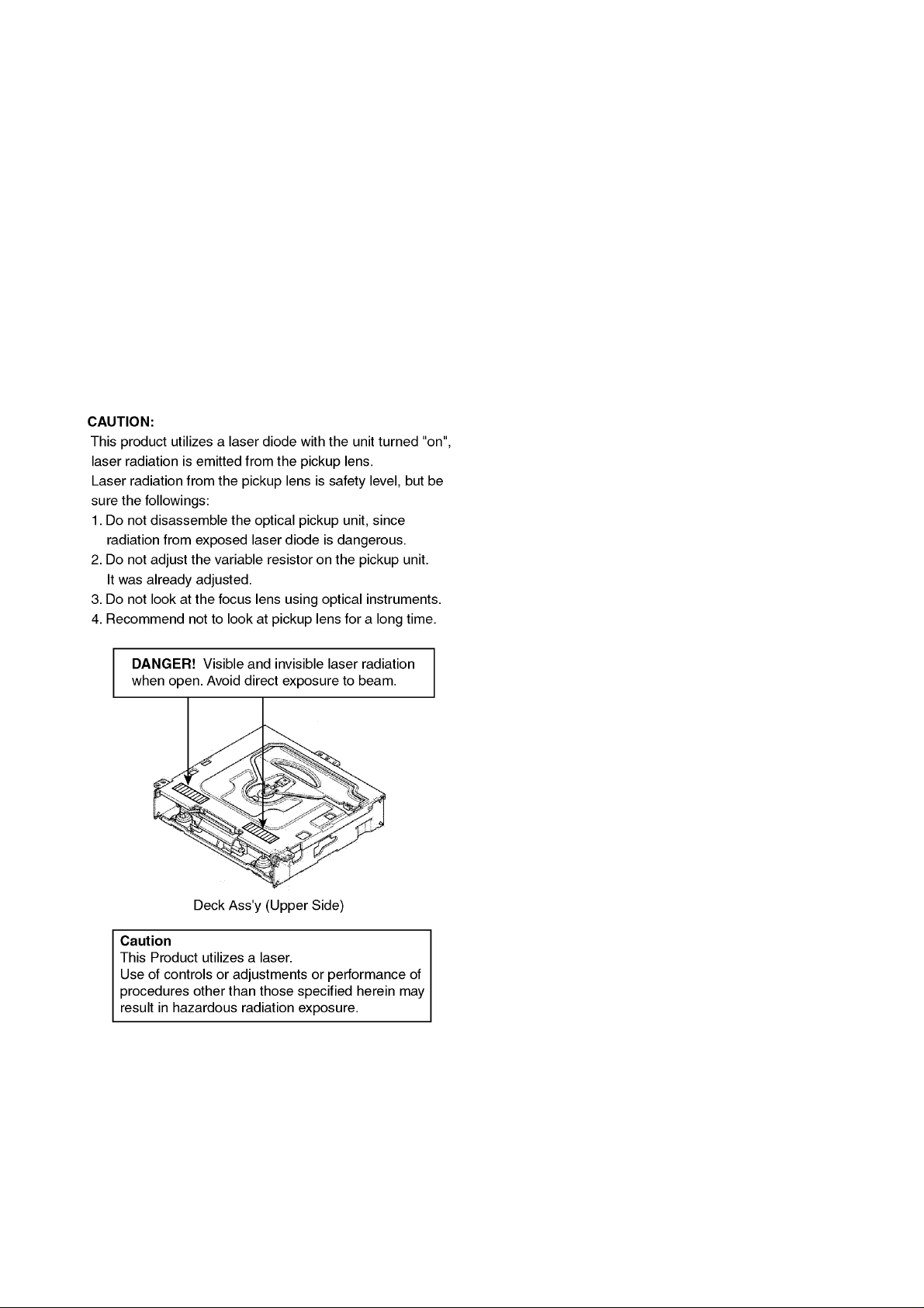
1.2. Laser Products
1.4. Maintenance
Your product is designed and manufactured to ensure a minimum of maintenance. Use a dry, a soft cloth for routine exterior
cleaning. Never use benzine, thinner or other solvents.
1.5. Notes
[RADIO BLOCK]
Do not align the AM/FM package block. When the package
block is necessary, it will be supplied alrea dy alig ned at the factory.
[CD DECK BLOCK]
This model has no servo alignment points because microcomputer controls the servo circuit.
1.3. Replacing the Fuse
Use fuses of the same s pe cif ied rati ng 15 a mps. Using different
substitutes or fuses with higher ratings, or connecting the unit
directly without a fu se, could cause fire or damage to th e st ere o
unit.
2
2 Specifications
2.1. Specifications*
General
Power Supply DC 12V (11V - 16V)
Current Consumption Less than 2.1A
Maximum Power Output 50W × 4 channels (at 1kHz),
Power Output 22 W x 4 channels (DIN 45 324, at 4 Ω)
Tone/SQ Adjustment Range SQ Low/Bass:±12dB
Speaker Impedance 4 - 8 Ω
Pre-amp Output Voltage 2.0 V
Pre-amp Output Impedance 200 Ω
USB Connector [CQ-RX300N only]
USB Standard Compatibili ty 1.1/2.0 Full Speed
Maximum Supply Current 500 mA
Front AUX Input
Input Impedance
Allowable External Input
Connector
Test Voltage 14.4V
Negative Ground
(CD mode, 0.5W 4 channels)
volume control maximum
(at 60 Hz, 80 Hz, 100 Hz, 200Hz)
SQ Mid: ±12 dB
(at 500 Hz, 1 kHz, 2 kHz, 3kHz)
SQ High/Treble: ±12 dB
(at 10kHz, 12kHz, 15 kHz, 18 kHz)
(CD mode: 1 kHz, 0 dB)
10 kΩ
2.0 V
3.5 mm Stereo mini-pin
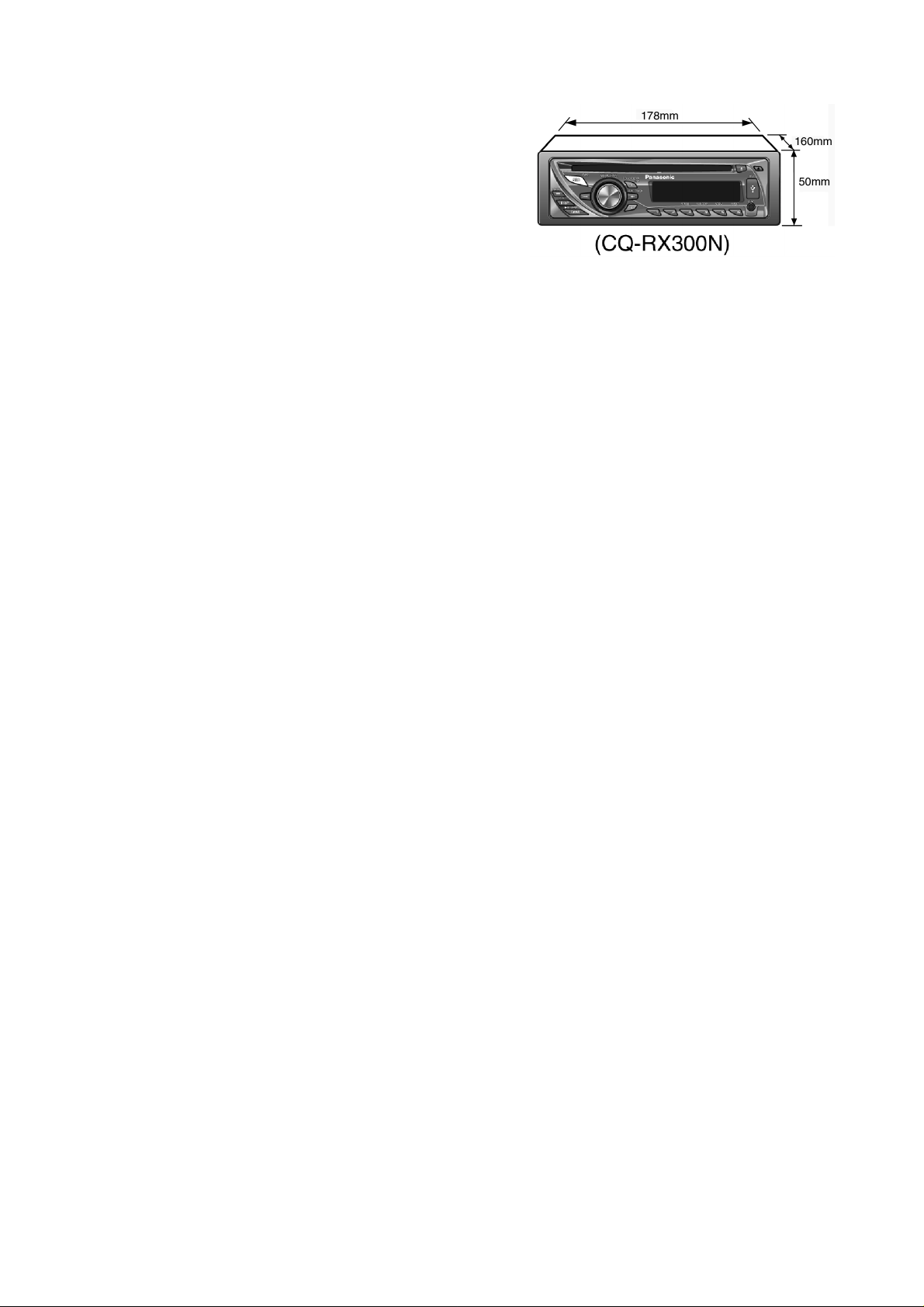
2.2. Dimensions
Dimensions (W×H×D)** 178×50×160mm
Weight** 1.2 kg
Disc Player
Sampling Frequency 8 times oversampling
DA Converter 1 bit DAC System
Pick-Up Type Astigma 3-beam
Light Source Semiconductor Laser
Wave Length 790 nm
Frequency Response 20 Hz - 20 kHz (±1 dB)
Signal to Noise Ratio 96 dB
Total Harmonic Distortion 0.01 % (1 kHz)
Wow and Flutter Below Measurable Limits
Channel Separation 85 dB
FM Radio
Frequency Range 87.5 MHz - 108.0 MHz
Usable Sensitivity 6 dB/µV (S/N 30 dB)
Stereo Separation 35 dB (at 1 kHz)
AM (MW) Radio
Frequency Range 531 kHz - 1602 kHz
Usable Sensitivity 28 dB/µV (S/N 20 dB)
AM (LW) Radio
Frequency Range 153 kHz - 279 kHz
Usable Sensitivity 32 dB/µV (S/N 20 dB)
* Specifications and the design are subject to possible modification
without notice due to improvements.
** Dimensions and Weight shown are approximate.
** Above specifications comply with EIA standards.
3
3 Features
• SQ3 (3-Band Sound Quality).
• USB Connector [CQ-RX300N only]
• The AUX Input terminal is equipped on the front panel.
• Expansion Module (The optional Hub unit: CY-EM100N)
[CQ-RX300N, CQ-RX200N only].
• The optional adapter (Direct Cable for iPod, CA-DC300N)
allows you to connect the optional iPod® series.
• The optional adapter (Conversion Cable for DVD/CD
Changer:CA-CC30N) allows you to connect the optional
Panasonic CD changer unit (CX-DP880 N ).
• Hands Free Phone System. (The optional Bluetooth handsfree kit: CY-BT200N)
• AAC/MP3/WMA Playback from CD-R/RW(CQ-RX300N
only).
• MP3/WMA Playback from CD-R/RW(Other).
• Anti-Theft System.
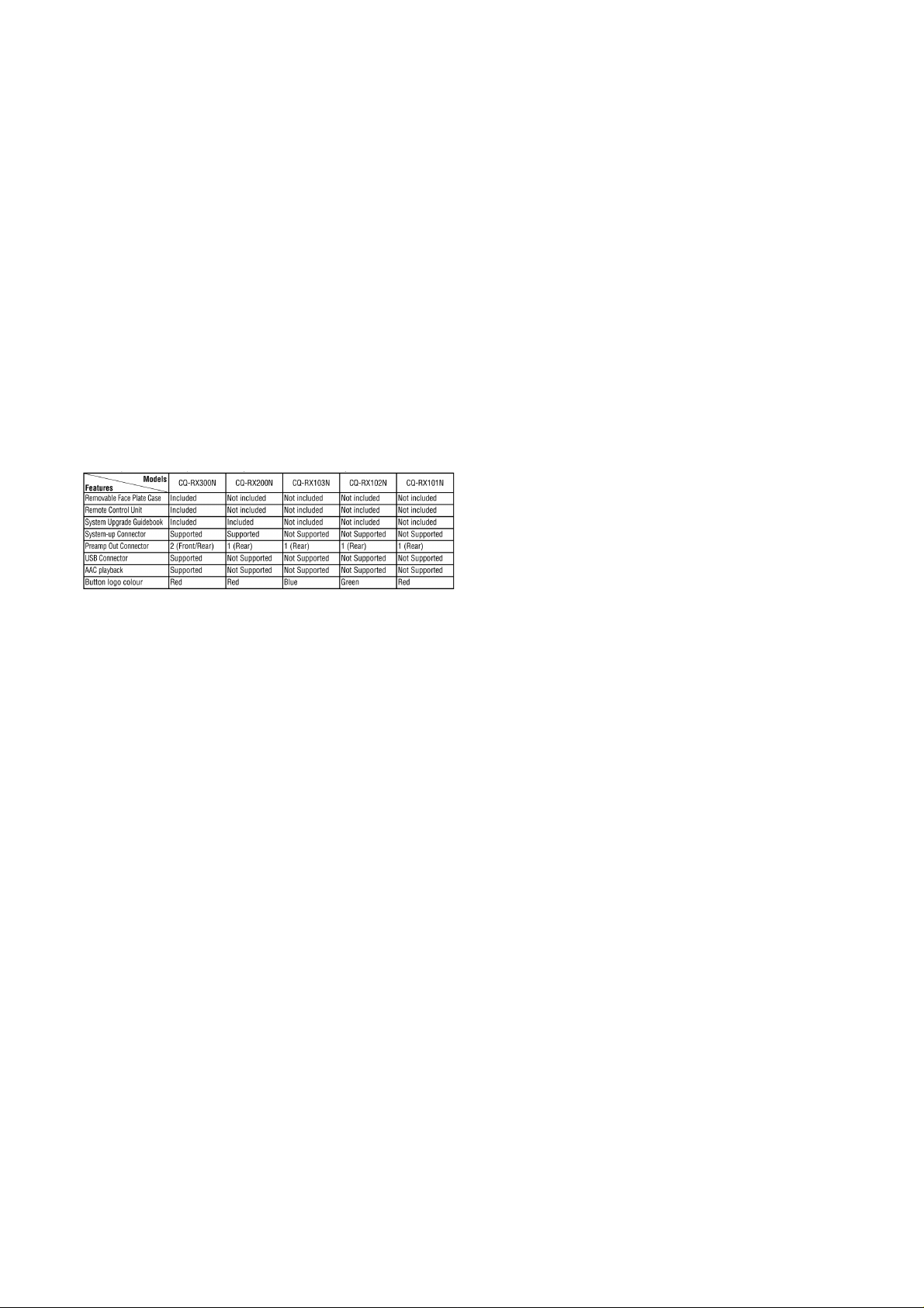
• This manual is for 5 models CQ-RX300N, CQ-RX200N, CQRX103N, CQ-RX102N and CQ-RX101N. The following table
describes the differences between 5 models.
4
4 Technical Descriptions
4.1. Terminals Description
4.1.1. Main Block
IC601 : YESAM433
Pin
No
1DBGP0 Not used -000
2DBGP1 Not used -000
3DBGP2 Not used -000
4 RDS CLK RDS (Radio Data Sys-
5 RM DATA Remote control data I 4.6 4.6 4.6
6 CDC STB/
7 EVENT Hub event detection
8 RESET Syst em reset I 4.9 4.9 4.9
9 XT1 Crystal oscillator 1
10 XT2 Crystal oscillator 2
11 VSS Ground - 0 0 0
12 CF1 Ceramic oscillator 1
13 CF2 Ceramic oscillator 2
14 VDD +5V power supply - 5. 0 5.0 5. 0
15 INI A Initialization mode A
16 VSM Signal meter intensity
17 INI B Initialization mode B
18 USB FLG Thermal shutdown flag
19 USB RESET USB reset (RX300N) O 0 0 0
20 NC Not connected - 0 0 0
21 SYSID1 Hub connection device ID
22 SYSID2 Hub connection device ID
23 USB MUTE USB mute (RX300N) O 0 0 0
24 CDC DATA Serial data from CD
25 CDC CLK/
26 CD DI (CD SI) Serial data to CD and USB
27 CD DO (CD
28 CD CLK Serial clock for CD and
29 CD CE (FS) Chip enable for CD and
30 NC Not connected - 0 0 0
31 NC Not connected - 0 0 0
32 NC Not connected - 0 0 0
33 SUB READY0 Sub ready from CD servo I 5.1 5.1 4.9
34 REG READY0 Reg. ready from CD servo I 5.1 5.1 0
35 CD SW1 CD detection switch 1 I 4.9 4.9 4.9
Port Description I/O Vol [V]
I 2.5 2.5 2.5
tem) clock
SYSID4
SYSID3
SO)
CD changer Strobe; or
Hub connection device ID
4 (RX200N/RX300N)
(RX200N/RX300N)
(32.768kHz)
(32.768kHz)
(13.50MHz)
(13.50MHz)
(RX200N: Pulled up; Others Pulled down)
(Tuner)
(Pulled down)
from USB regulator
(RX300N)
1 (RX200N/RX300N)
2 (RX200N/RX300N)
changer (RX200N/
RX300N)
Serial clock for CD
changer; or Hub connection device ID 3 (RX200N/
RX300N)
(USB: RX300N)
Serial data from CD and
USB (USB: RX300N)
USB (USB: RX300N)
USB (USB: RX300N)
I000
I000
I 1.0 1.0 1.0
O 1.4 1.4 1.4
I 1.4 1.4 1.4
O 1.3 1.3 1.3
I 4.9 4.9 4.9
I000
I000
I000
I 5.0 5.0 5.0
I 5.0 5.0 5.0
I000
I000
O0 03.0
I 3.2 3.2 2.2
O0 03.0
O0 00.9
FM AM CD
Pin
No
36 CD SW2 CD detection switch 2 I 4.9 4.9 4.9
37 CD DMUTE CD mute I 0 0 5.1
38 CD LIMIT SW CD limit detection switch I 5.1 5.1 5.1
39 VSS Ground - 0 0 0
40 VDD +5V power supply - 4.9 4.9 4.9
41 CD MUTE Mute for Pick-up driver O 0 0 0
42 CD S/L CD Sleding/Loading mode
43 CD F/R CD loading direction: For-
44 CD RESET CD reset O 4.9 4.9 4.9
45 HUB ACC
46 HUB CNT Hub connection check
47 USB ENBL USB enable (RX300N) O 0 0 0
48 USB SLP USB sleep (RX300N) O 0 0 0
49 LCD DI Serial data to LCD O 4.9 4.9 4.9
50 LCD DO Serial data from LCD I 4.3 4.3 4.3
51 LCD CLK Serial clock for LCD O 4.9 4.9 4.9
52 LCD CE Chip enable for LCD CPU O 0 0 0
53 E-VOL I2C
54 E-VOL I2C
55 VDD +5V power supply - 4.9 4.9 4.9
56 VSS Ground - 0 0 0
57 E-VOL MUTE Not connected - 0 0 0
58 POWER CNT Syst em power supply con-
59 STBY Standby mode for Power
60 NC Not connected - 0 0 0
61 NC Not connected - 0 0 0
62 SUB CLK
63 NC Not connected - 0 0 0
64 BEEP Beep tone (RX200N/
65 USB IN USB-in detection
66 ACC ACC level detection I 5.2 5.2 5.2
67 NC Not connected - 0 0 0
68 MODE B Rotary encoder detection
69 MODE A Rotary encoder detection
70 EXT MUTE Not connected - 0 0 0
71 PANEL IN Front panel detection I 4.9 4.9 4.9
72 BATT Battery level detection I 4.6 4.6 4.6
73 RDS DATA RDS (Radio Data Sys-
74 CDC REM
75 HUB-TX Transmission data to Hub
76 HUB-RX Reception data from Hub
77 USB RXD Serial data to USB
78 USB TXD Serial data from USB
79 FM MODE Power supply control for
Port Description I/O Vol [V]
O4.94.94.9
switch
O000
O000
O4.94.94.9
O4.94.94.9
O4.94.94.9
O4.94.94.9
O4.94.94.9
O000
I000
I5.05.05.0
I5.05.05.0
I2.5 0 0
O000
O000
I000
O000
I000
O4.9 0 0
CNT
DATA
CLK
OUT
OUT
ward/Reverse
Power supply control for
Hub (External device)
(RX200N/RX300N)
request (RX200N/
RX300N)
Serial data for Audio signal processor (volume)
Serial clock for Audio signal processor
trol
amplifier
Not connected - 0 0 0
RX300N)
(RX300N)
B for volume
A for volume
tem) data
Remote control for CD
changer (RX200N/
RX300N)
(RX200N/RX300N)
(RX200N/RX300N)
(RX300N)
(RX300N)
FM mode
FM AM CD
5
Pin
No
80 AM MODE Power supply control for
81 MONO Monaural control O 0 0 0
82 ST FM stereo indication I 5.1 5.1 5.1
83 DI/DO Not connected - 0 0 0
84 CS Not connected - 0 0 0
85 SK Not connected - 0 0 0
86 NC Not connected - 0 0 0
87 VREG Connected to capacitor - 3.0 3.0 3.0
88 VSS Ground - 0 0 0
89 VDD (PLL) +5V power supply - 5. 0 5.0 5.0
90 OSC FM/AM FM/AM local oscillation
91 NC Ground - 0 0 0
92 FM/AM IFC FM/AM center frequency I 0 0 0
93 NC Ground - 0 0 0
94 EO FM/AM phase detection
95 SUBPD Not connected - 0 0 0
96 SSC SD sensitivity control O 0 0 0
97 ANT CNT Not connected - 4.9 4.9 4.9
98 AMP CNT Power supply control for
99 AF MUTE Audio signal mute O 0 0 0
100 AMP MUTE Mute for Power amplifier O 4.9 4.9 4.9
Port Description I/O Vol [V]
FM AM CD
O04.90
AM mode
I 1.4 1.4 1.4
frequency
O 2.2 2.2 2.2
error
O 4.9 4.9 4.9
External amplifier
6
4.2. IC Block Diagram
4.2.1. Main Block
IC201 : YESAM440
IC271 : YESAM438 (CQ-RX300N only)
IC271 : C1EA00000041
(Other)
IC501 : YESAM425
IC671 : YESAM391
7
IC751 : YESAM424
IC801 : YESAM429 (CQ-RX300N only)
IC801 : YESAM428 (Other)
8
IC771 : YESAM426 (CQ-RX300N only)
IC791 : YESAM344 (CQ-RX300N,RX200N only)
IC852 : YESAM439
PA051 : YESAP403
4.2.2. Display Block
IC851 : YESAM437
IC901 : YESAM427
IC902 : YESAM264
9
5 Block Diagram
5.1. Main-1 Block
AT51
XL501
4.332MHz
IC501
13
RDS
DEM
14
FM / AM TUNER
AM ANT
1
2 FM ANT
FM VT
PA51
AM VT
16
2
4
RX300N/RX200N
ONLY
HUB L
24
AUX L
FM DET
16
L-CH
R-CH R-CH
212011146
17
22 23
CD L
FRONTRX300N
REAR
ONLY
LR
LR
7231-02-21(1/3)
CN250
CN701
BATT
IC201
AUDIO SIGNAL PROCESSOR
MUTE
R-CH
Q365
MUTE
5
3
INPUT
7
SEL
VOLUME
TONE
FADER
1
FL
16
RL
15
Q366
R-CH
SW
Q261
POWER AMP
12
14
IC271
5
3
21
23
FL+
FL-
RL+
RL-
ACC
AMP CNT
R-CH
FR+
FR-
21
43
65
87
10 9
1211
SDA
SCLK
1819
STBY
MUTE
R-CH
224
RR+
RR-
1413
Q401
FM / AM OSC
EO
VSM
SD / ST IND
FM / AM IFC
16929094
FM ST/MONO
82
81
Q54
DATA
RDS
473
SCLK
TU+B
Q52,602
POW
POW
Q55,601
SW
SW
80
AM MODE
FM VCC
AM VCC
79
FM MODE
5453
SDA
E-VOL
I2C
SCLK
IC601(1/3) SYSTEM CONTROL
XL602
32.8KHz
9
XT110XT2
XL601
Q251
REM IN
BAT DET
1615
13.5KHz
RX300N
ONLY
59
12
CF113CF2
99
AF MUTE
100
STBY
AMP MUTE
CQ-RX300N/RX200N/RX103N/RX102N/RX101N MAIN (1/3)
10
5.2. Main-2/D is pl ay Block
7231-05-11 7231-02-21(2/3)
RX300N/RX200N ONLY
LD901
KEY-IN
MATRIX
IC901
LCD DRIVE
SEG
1–34
3–36
COM
1–4
KS
3–6
KI
2–5
50–53 45–48 39–42
Q902
LED
DRIVE
CN902
AUX
IC601(2/3)
SYSTEM CONTROL
CN971CN901
DI
DO
CL
CE
64
61
63
62
10
11
13
12
10
11
13
12
49
LCD DI
50
LCD DO
51
LCD CLK
52
LCD CE
HUB TX
HUB RX
CDC DATA
CDC REMO
CDC CLK
VDD
54
Q901
5
5
VDD5V2
CDC STB
HUB CNT
EVENT
P1
1
PWR
SW
71
6
6
PANEL
IC701
5V
P2
2
SOURCE
D901
BATT
BATT
CHECK
15
3
72
8
BATT
RESET
64BEEP
75
76
24
74
25
6
46
7
21
22
HUB L
BATT
6
3
8
12
11
2
1
IC671
INV
IC791
15V
LIMIT
R-CH
5
4
9
13
10
1
3
L-CH
R-CH
DATA
REMO
SCLK
STRB
HCNT
EVENT
SYS ID1
SYS ID2
ACC
CN671
3
456
78910
11 12
2131
BAT DET
2
RECEIVE
L-CH
IC902
IR
SW901
9
1
9
8
8
7
7
2
2
RX300N ONLY
REMO
REM IN
MODE A
MODE B
AUX L
5
RM DATA
69
MODE A
68
MODE B
USB
ENBL17FLG
HUB ACC
CNT
ACC
AMP CNT
PWR CNT
45
66
98
58
BATT
ACC
IC751
POWER SUPPLY
9
VCC
3
ACC
2
COMP
MODE 2
11
MODE 1
6
1
4
10
13
BATT
SW5V
VDD5V2 VDD5V1
Q752
POW
SW
AMP CNT
Q770
AUD9V TU+B
DELAY
START
47
Q751
R-CH
DSP
12
POW
SW
DSP3.3V
USB
3
2
1
CN903
D+
D–
VBUS
ILL10V
17
18
20
1515
17
18
20
D+
D–
IC781 IC771
1
3
POW
54
SW
11
15
ILM
CD
7
CD+B
4
5V
21
REG
BATT
RX300N
ONLY
CQ-RX300N/RX200N/RX103N/RX102N/RX101N MAIN(2/3)/DISPLAY
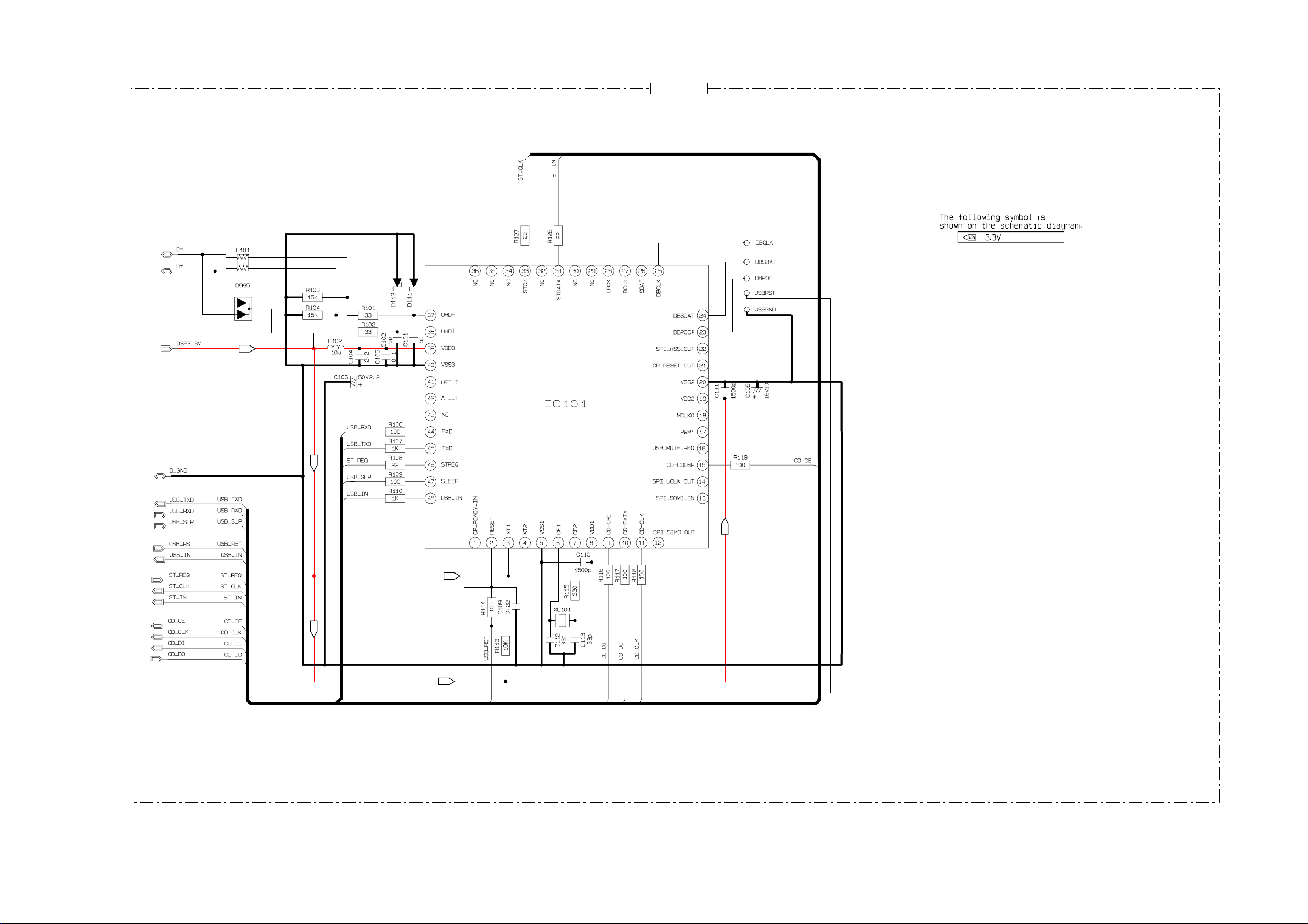
5.3. Main-3/CD Interface Block
7231-02-21(3/3)3032-14-53Optical Pic-up Ass'y
IC801
CN2 CN1
A
B
E
F
PD
LD
I-V
AMP
7
9
3
2
11
4
10
1
A
B
E
F
LPD
LD3.3V
VREF
VCC
21
22
CN801
1
1
3
3
4
4
2
2
8
8
Q871
21
6
6
22
LD
DRIVE
DSP3.3V
PICK-UP DRIVE
5
6
7
8
14
13
19
18
VREF
11
IC851
A
C
B
D
F
E
LDS
LDO
-
-
RF AMP,SERVO,DSP
+
FE
ADC
TE
SERVO
CTL
FDO
TDO
SLDO
SPDO
EFM
DEM
LIMIT SW
X IN
733224252322
XL801
16.93MHz
X OUT
72
DAC
48
34
49
33
L-CH
R-CH
ST-IN
ST-CLK
ST-REQ
CONT0
DO
DI
CL
CE
50
47
37
44
27
R-CH
26 28
CD L
IC601(3/3)
SYSTEM
CONTROL
29
76
78
56
55
54
52 18
46
45
44
43
RX300N ONLY
USB CONTROL
28
LRCK
27
STCLK
26
SDAT
31
ST DATA
33
ST CK
46
ST REQ
MCLKD
10
CD DATA
9
CD CMD
11
CD CLK
15
CE CD DSP
IC101
UHD+
UHD-
CF1
CF2
38
37
D+
D–
XL101
6
7
FOCUS
COIL
TRACKING
COIL
SPINDLE
MOTOR
SLED
MOTOR
F+
T+
SP-
SL+
SL-
14
16
18
20
10
12
17
15
19
14
16
18
20
10
12
7
7
5
5
17
15
19
F-
T-
16
15
14
13
M
SP+
M
CD SW1
CD SW2
CD LIMIT SW
2
1
26
27
11
12
17
18
FOCUS
COIL
DRIVE
TRACKING
COIL
DRIVE
SPINDLE
MOTOR
DRIVE
SLED
MOTOR
DRIVE
MUTE
24
20
4
SUB READY
REG READY
7
9
IC852
6
15
7
41 CD DMUTE
CD S/L
42
35 CD SW1
43 CD F/R
36 CD SW2
38 CD LIMIT SW
CD MUTE
CD RESET
CD DI
CD DO
CD CLK
USB TXD
USB RXD
USB RESET
USB MUTE
USB IN
USB SLP
CD CE
78
77
19
23
65
48
45
TXD
44
RXD
2
RESET
USB MUTE REQ
16
USB IN
48
SLEEP
47
CQ-RX300N/RX200N/RX103N/RX102N/RX101N MAIN(3/3)
12
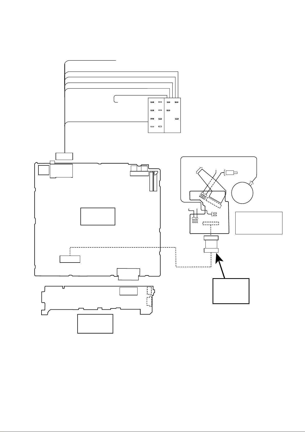
6 Wiring Connection Diagram
6.1. [CQ-RX300N]
External Remote Control
Power (ACC or IGN)
Ground
Motor Antenna Relay Control
Battery(15A)
14
13
12
11
CN671
12
16
15
13 1
CN701
Power
Connector
2
[7231-02-11]
Speaker
Main P.C.B
Not Used
Preamp Out
(Front) (Rear)
31
2
CN250
64
5
AT051
RL+
FL+
FR+
RR+
RL-
FL-
FR-
RR-
ACC
Motor
ANT
GND
BATT
Optical
Pic-Up
Ass'y
SW2
SW1
Loading/Feed
Limit
SW
Motor
Spindle
Motor
1
CN2
16
22
2
CN1
1
21
CD Interface P.C.B
[3032-14-53]
(Bottom View)
22
21
CN801
2
1
Display P.C.B
[7231-05-11]
(Bottom View)
19
20
19
20
CN971
CN901
2
2
1
1
CN902
CN903
AUX
54
4
1
3
1
2
Connector
Jig Part No.
[YESFZS2076]
Extension
13
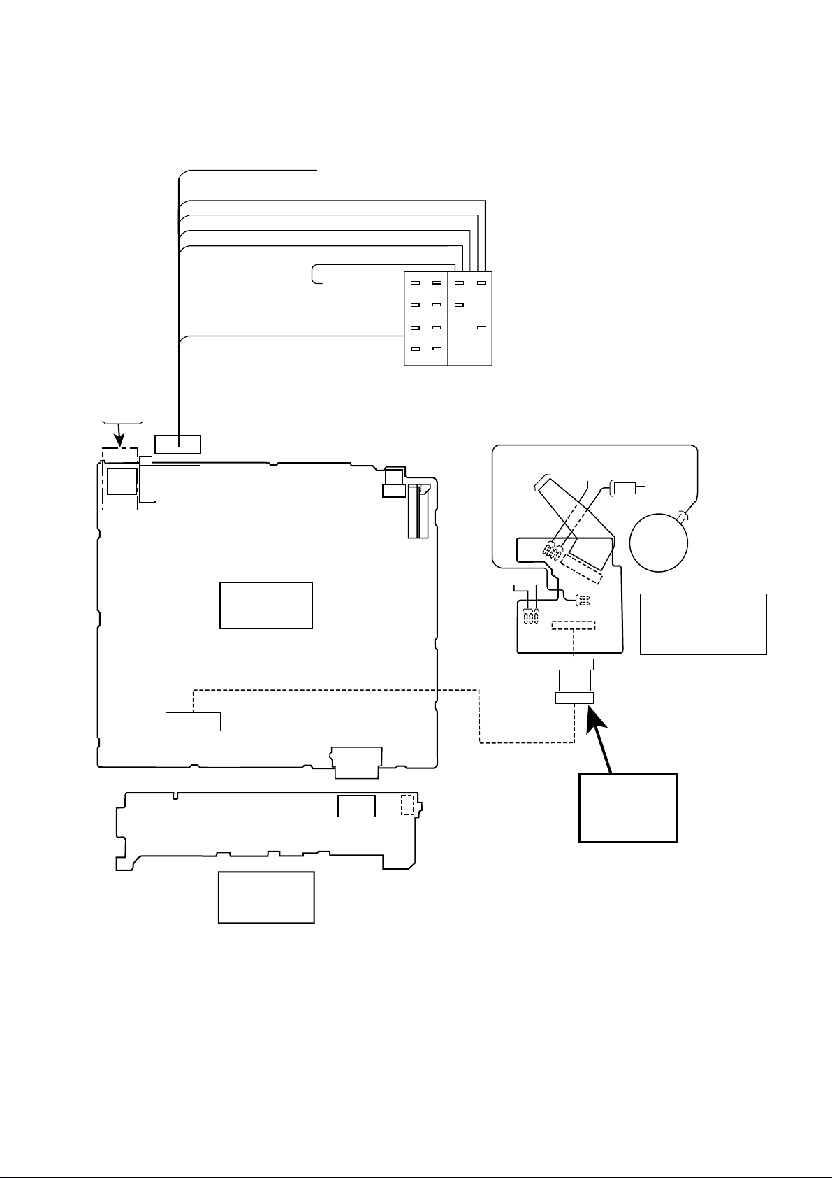
6.2. [CQ-RX200N/RX103N/RX102N/RX101N]
External Remote Control
Power (ACC or IGN)
Ground
Motor Antenna Relay Control
Battery(15A)
CQ-RX200N
only
14
12
13
12
11
15
CN671
16
13 1
CN701
Power
Connector
2
[7231-02-11]
Speaker
Main P.C.B
Not Used
RL+
FL+
FR+
RR+
Preamp Out
(Rear)
CN250
AT051
RL-
FL-
FR-
RR-
ACC
Motor
ANT
GND
BATT
Optical
Pic-Up
Ass'y
SW2
SW1
Loading/Feed
Limit
SW
Motor
Spindle
Motor
1
CN2
16
22
2
CN1
1
21
CD Interface P.C.B
[3032-14-53]
(Bottom View)
22
21
CN801
2
1
Display P.C.B
[7231-05-11]
(Bottom View)
15
CN971
15
CN901
2
1
1
CN902
2
AUX
54
3
1
2
Extension
Connector
Jig Part No.
[YESFZS2076]
14
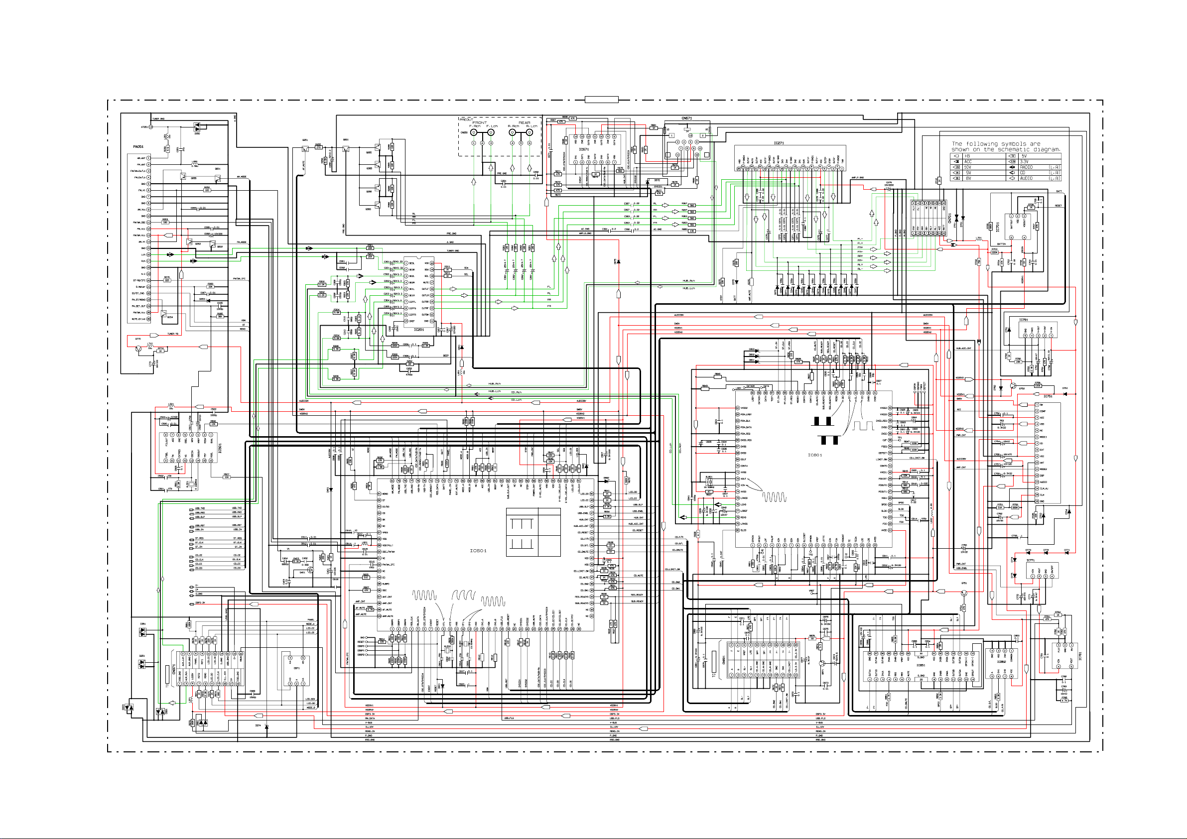
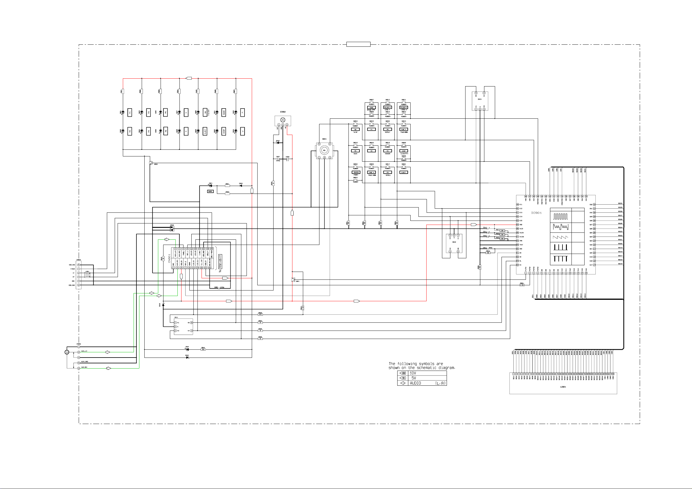
7 Schematic Diagram
7.1. Main-1 Block[CQ-RX300N]
7231-02-11
YESAP403
YESAN149
8.0
7.2
YESAD155
0
0
0
8.2
0
1.3
0
0
0
0
0
8.1
8.1
8V
1.3
0
L
3.6
3.6
0
0
0
5.1
0
0
0
8.1
0
0
YESAN152
8V
8.0
8.1
8.1
8V
8.2
YESAN154
R
0
YESAN154
YESAN152
8.1
0
0
0
4.9
0
YESAN152
YESAD188
9V
YESAN153
5.0
0
5.0
L
YESAN153
0
0
0
R
0.022
0.022
0
0
0
YESAN155
0
0
0
YESAN155
YESAN155
YESAN155
0
0
0
0
0
0
L
L
R
R
5V
L
3.2
8.8
3.2
5.0
L
R
L
R
L
3.2
3.2
3.2
3.2
3.2
3.2
3.2
3.2
YESAM440
5.0
4.0
L
L
4.0
4.0
4.0
0
R
R
L
R
R
R
YESAD167
9V
R
L
5V
9V
5V
L
R
L
9V
5V
R
YESAM425
YESAD144
Pin No.
Waveform
PIN49
2V/DIV,10mS/DIV
PIN51,PIN52
1.3
YESAM433
2.2
0
L
B1CBGF000005
R
3.3V
10
0.5V/DIV,10uS/DIV
1V/DIV,10uS/DIV
2V/DIV,50mS/DIV
1V/DIV,20nS/DIV
0
0
0
5.0
5.0
5.0
4.9
YESAM391
0
4.0
5.0
YESAD133
YESAD133
0
0
0
5V
5V
YESAD144
5V
YESAD188
0
L
R
L
R
L
R
R
L
5V
47K
3.3V
6.3V330
R
5V
YESAD143
47K
3.1
0
1.5
0
3.1
0
1.5
1.5
3.1
3.1
L
1.5
1.5
1.5
0
1.6
7.3
7.3
7.2
7.3
7.3
4.9
14.4
L
R
R
L
50V2.2
47K
YESAD192
9V
5V
YESAD187
YESAD187
YESAD187
0
0
1V/DIV,20nS/DIV
1.5
2.1
1.6
1.6
1.7
3.3V
0
4.9
YESAM438
0
7.3
R
YESAD192
0
7.4
R
5V
47K
5.1
1V/DIV,5uS/DIV
1.6
7.3
14.4
L
16V22
YESAD192
4.9
1V/DIV,5uS/DIV
0
5.0
YESAD192
0
1.9
0
7.3
L
AMP,
L
ANT_CNT
REMO_IN
YESRTD016
YESAD193
L
R
R
R
R
L
L
YESAD192
YESAD192
3.3V
3.1
00
0.9
3.0
3.0
2.2
4.9
1V/DIV,10mS/DIV
1.6
1.9
1.6
3.2
2.4
0
3.1
1.5
0
3.1
3.1
0
5.1
3.1
1.1
1.2
1.2
0
1.7
1.6
1.6
1.5
3.2
0
0
3.3V
3.3V
5V
6.3V330
3.3V
3.3V
YESLT032
5V
5V
5V
5V
5V
5V
8V
YESAN157
3.3
3.3
4.0
5V
YESAM441
YESAD192
3.3V
4.9
0
4.6
5.0
5.0
YESAM344
YESAD192
0
0
0
0
14.3
5.0
5.6
4.9
YESAN079
5V
5V
8V
14.0
9V
13.4
10V
YESAD192
YESAD192
YESAD192
5.1
5.2
6.4
5.0
4.9
8.0
4.9
3.2
9.1
1.2
9.5
0
YESAM424
YESAD196
YESAD192
YESAM426
5V
YESAD197
YESAD198
YESAD197
0
7.2
7.2
7.3
7.3
7.2
YESAD192
YESAD192
5V
3.1
2.3
0
YESAM429
1.7
1.8
1.7
1.7
YESAD191
YESAD191
YESAD155
CN901
7231-05-11
YESAD155
5V
3.3V
1/4W
CN1
47K
47K
YESAD150
R
10V
YESAD149
YESAD189
YESAD143
5V
5V
3.3V
10V
3032-14-53
1/4W
3.2
3.2
0
YESAN156
3.3V
3.8
3.5
0
8.0
1.6
1.6
YESAM437
3.4
3.8
1.6
4.9
8V
1.5
0
0
0
8.0
1.6
0
1.6
7.4
3.6
3.6
3.3
3.9
YESAM439
1.605.1
5.0
0
7.4
10V
YESAM400
CQ-RX300N MAIN 1/2
15
7.2. Main-2 Block[CQ-RX300N]
YESAD189
3.3V
YESAD187
YESAD187
7231-02-11
3.3V
3.3V
YESAM435
3.3V
3.3V
3.3V
16
CQ-RX300N MAIN 2/2
7.3. Display Block[CQ-RX300N]
7231-05-11
10V
680
YESAD185
YESAD185
680
YESAD185
YESAD185
YESAN150
YESAD185
YESAD185
YESAD185
YESAD185
680
YESAD185
YESAD185
YESAD185
680
YESAD185
YESAD185
CN971
1.3k
YESAD190
YESAD185
YESAD185
1.5k
YESAD143
820
10V
YESAM264
4.3
YESAD189
0
4.3
YESAS133
5.0
5.0
5.0
0
5V
5V
YESAD190
0
0
YESAM427
0
5.0
5.0
5.0
1.6
0
0
0
4.2
0
4.9
4.8
2.5
2.5
5.0
2.5
2.5
Waveform
0.5V/DIV,1mS/DIV
0.5V/DIV,1mS/DIV
1V/DIV,10uS/DIV
2V/DIV,5mS/DIV
2V/DIV,5mS/DIV
2.5
Pin No.
PIN3-PIN36
PIN39-PIN42
PIN60
PIN62
PIN63,PIN64
2.5
2.5
2.5
2.5
2.5
2.5
2.5
2.5
2.5
2.5
2.5
2.5
2.5
2.5
2.4
2.5
2.5
2.5
2.5
680
680
YESAD155
L
5V
10V
5.0
4.2
YESAN151
5.0
4.2
2.5
2.5
4.8
2.5
2.5
2.4
2.4
2.5
2.5
2.5
2.5
2.5
2.5
2.5
2.5
L
R
YESAD189
YESAD150
L
YESAD180
YESAD186
1/4W
5V 5V
R
YESXDCM043
CQ-RX300N DISPLAY
17
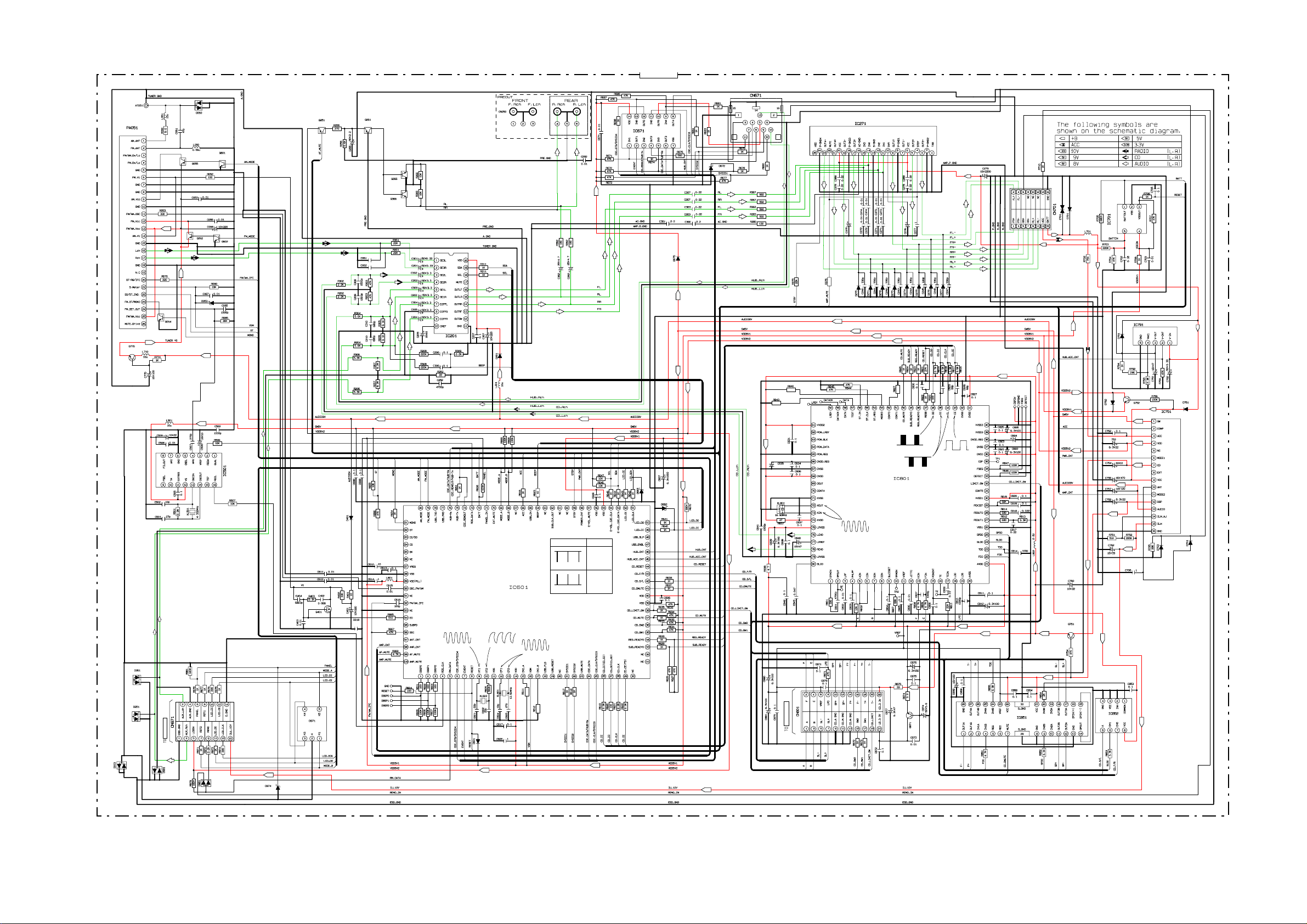
7.4. Main Block[CQ-RX200N]
7231-02-11
YESAP403
YESAN149
8.0
7.2
YESAD155
0
0
0
8.2
0
1.3
0
0
0
0
0
8.1
8.1
8V
1.3
0
L
3.6
3.6
0
0
0
5.1
0
0
0
8.1
0
0
YESAN152
8V
8.0
YESAN152
8.2
8.1
YESAN154
8.1
YESAN154
8.1
0
0
0
0
4.9
0
YESAN152
R
8V
YESAD188
9V
YESAN153
5.0
0
5.0
L
YESAN153
0
0
0
L
0
0
0
YESAN155
0
0
0
YESAN155
R
0.022
0.022
L
R
L
R
L
3.2
3.2
3.2
3.2
3.2
3.2
3.2
3.2
3.2
3.2
YESAM440
8.8
5.0
5.0
4.0
L
L
4.0
4.0
4.0
0
R
5V
L
L
R
R
R
R
R
YESAD167
9V
R
L
5V
9V
5V
L
R
L
9V
5V
R
YESAM425
YESAD144
Pin No.
Waveform
PIN49
2V/DIV,10mS/DIV
PIN51,PIN52
1.3
YESAM433
2.2
0
L
B1CBGF000005
R
1000p
0.5V/DIV,10uS/DIV
1V/DIV,10uS/DIV
2V/DIV,50mS/DIV
1V/DIV,20nS/DIV
0
0
0
5.0
5.0
5.0
4.9
YESAM391
0
4.0
5.0
YESAD133
YESAD133
0
0
0
5V
5V
YESAD144
5V
YESAD188
0
L
R
L
R
L
R
R
L
5V
R
5V
47K
47K
3.1
3.3V
6.3V100
0
1.5
0
3.1
0
1.5
1.5
3.1
3.1
L
1.5
1.5
1.5
0
1.6
7.3
7.3
7.3
7.3
4.9
14.4
L
R
R
L
16V10
12K
9V
5V
0
1V/DIV,20nS/DIV
1.5
2.1
1.6
1.6
3.3V
0
4.9
7.2
7.2
YESAD192
0
1.7
7.2
YESAD192
0
1.7
0
2.3
1.7
7.2
5V
7.3
YESAD192
3.1
1.8
C1EA00000041
0
7.3
7.3
R
YESAD192
5V
47K
1V/DIV,5uS/DIV
YESAM428
1.7
7.4
R
5.1
1.6
14.4
16V22
YESAD192
5.0
7.3
L
YESAD192
0
4.9
1V/DIV,5uS/DIV
0
1.9
0
0
7.3
L
AMP,
L
ANT_CNT
REMO_IN
YESRTD016
YESAD193
4.9
0
4.6
L
R
R
R
R
L
L
YESAD192
YESAD192
3.3V
3.1
00
0.9
3.0
3.0
2.2
4.9
1V/DIV,10mS/DIV
1.6
1.9
1.6
3.2
2.4
0
3.1
1.5
0
3.1
3.1
0
5.1
3.1
1.1
1.2
1.2
0
1.7
1.6
1.6
1.5
3.2
0
0
3.3V
3.3V
5V
6.3V100
3.3V
3.3V
YESLT032
5V
5V
5V
5V
5V
5V
YESAN157
3.3
3.3
4.0
YESAM441
5.0
5.0
YESAM344
YESAD192
0
0
0
0
14.3
5.0
5.6
4.9
YESAN079
YESAD192
3.3V
8V
5V
5.1
5V
5.2
6.4
5.0
5V
4.9
8.0
8V
14.0
9V
13.4
4.9
3.2
9.1
1.2
9.5
10V
0
YESAM424
YESAD196
YESAD197
YESAD198
YESAD191
YESAD191
YESAD155
CN901
7231-05-11
R
YESAD155
YESAD149
YESAD189
5V
3.3V
47K
47K
YESAD150
YESAD143
10V
5V
5V
10V
CN1
3032-14-53
1/4W
1/4W
3.2
3.2
0
YESAN156
3.8
3.5
0
8.0
1.6
1.6
YESAM437
3.4
3.8
1.6
4.9
8V
1.5
0
0
0
8.0
1.6
0
1.6
7.4
3.6
3.6
3.3
3.9
YESAM439
1.605.1
5.0
0
7.4
10V
CQ-RX200N MAIN
18
 Loading...