

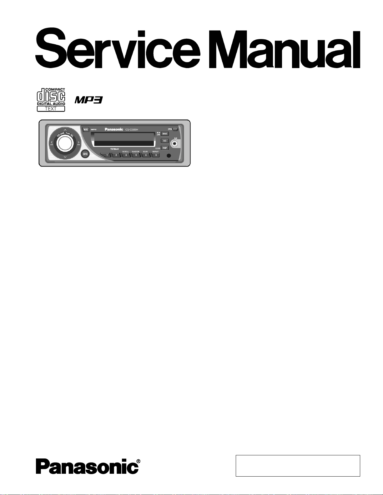
Panasonic CQC-3303-H Service manual
Specifications*
ORDER NO.ACED051230C3
AUTOMOTIVE AFTERMARKET
CQ-C3303H
MP3 CD Player/Receiver
General
Power Supply DC 12V (11V - 16V),
Test Voltage 14.4V
Negative Ground
Current Consumption Less than 2.1A (CD mode ; 0.5W
4-channels)
Maximum Power Output 50W×4ch (at 1kHz)
Power Output 18W×4ch (1kHz, 1%, 4Ω)
Tone Adjustment Range Bass ; ±12dB at 100Hz
Treble ; ±12dB at 10kHz
Speaker Impedance 4-8Ω
Pre-Amp Output Voltage 2.5V (CD mode; 1kHz, 0dB)
Pre-Amp Output Impedance 200Ω
Front AUX Input
Input Impedance 10kΩ
Allowable External Input 2.0V
Connector 3.5mm Stereo mini-pin
FM Stereo Radio
Frequency Range 87.5MHz - 108MHz
Usable Sensitivity 6dB/µV (S/N 30dB)
Frequency Response 30Hz-15kHz (±3dB)
Alternate Channel Selectivity 75dB
Stereo Separation 35dB (1kHz)
Image Rejection Ratio 70dB
IF Rejection Ratio 100dB
Signal to Noise Ratio 62dB
AM Radio
Frequency Range 531kHz - 1,602kHz
Usable Sensitivity 28dB/µV (S/N 20dB)
CD Player
Sampling Frequency 8 Times Oversampling
DA Converter 1bit DAC System
Pick-Up Type Astigma 3-beam
Light Source Semiconductor Laser
Wave Length 790nm
Frequency Response 20Hz to 20kHz (±1dB)
Signal to Noise Ratio 93dB
Total Harmonic Distortion 0.01% (1kHz)
Wow and Flutter Below measurable limits
Channel Separation 75dB
Dimensions** 178×50×160mm
Weight** 1.4kg
* Specifications and the design are subject to possible modification
without notice due to improvements.
** Dimensions and Weight shown are approximate.
•
• Above specifications comply with EIA standards.
• •
© 2 005 Matsushita Electric Industrial Co., Ltd. All
rights reserved. Unauthorized copying and
distribution is a violation of law.
CQ-C3303H
CONTENTS
Page Page
1 ABOUT LEAD FREE SOLDER (PbF) 3
2 LASER PRODUCTS
3 FEATUERS
4 REPLACING THE FUSE
5 MAINTENANCE
6 NOTES
7 DIMENSIONS
8 WIRING CONNECTION
9 TERMINALS DESCRIPTION
10 PACKAGE AND IC BLOCK DIAGRAM
11 REPLACEMENT PARTS LIST
3
3
12 EXPLODE D VIEW (Unit)
3
13 CD PLAYER PARTS LIST
14 EXPLODE D VIEW (CD Deck)
3
3
15 WIRING DIAGRAM
3
16 SCHEMATIC DIAGRAM -1
17 SCHEMATIC DIAGRAM -2
4
5
18 BLOCK DIAGRAM
7
9
14
15
16
17
21
23
25
2
CQ-C3303H
1 ABOUT LEAD FREE
SOLDER (PbF)
Distinction of PbF PCB:
PCBs (manufactured) using lead free solder will have a PbF
stamp on the PCB.
Caution :
•
• Pb free solder has a higher melting point than standard
• •
solder; Typically the melting point is 50 - 70°F (30 40°C) higher. Please use a soldering iron with
temperature control and adjust it to 700 ± 20°F (370 ±
10°C). In case of using high temperature soldering iron,
please be careful not to heat too long.
•
• Pb free solder will tend to splash when heated too high
• •
(about 1100°F/600°C)
•
• This lead free solder will be used for the products after
• •
serial No. 1,000,001.
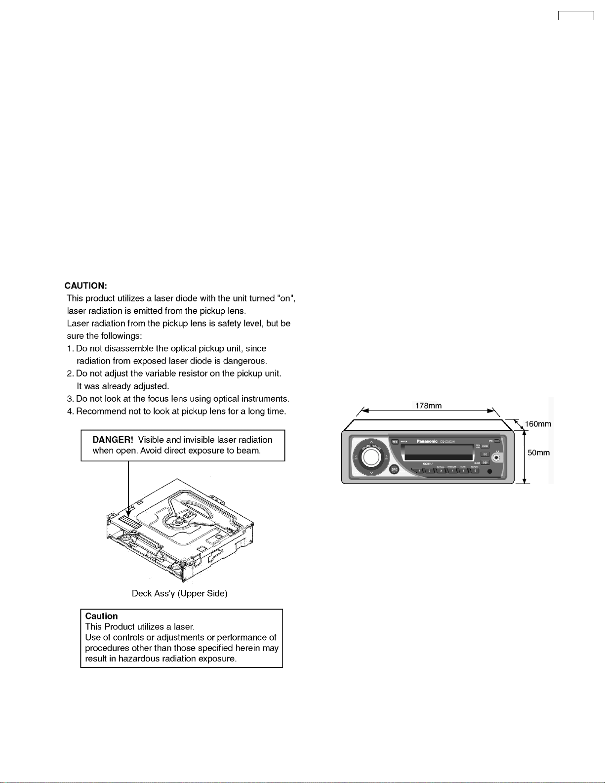
2 LASER PRODUCTS
3 FEATUERS
•
• Large-sized volume control.
• •
•
• SQ (Sound Quality).
• •
•
• The AUX input terminal is equipped on the front panel.
• •
4 REPLACING THE FUSE
Use fuses of the same specified rating (15amps). Using
different substitutes or fuses with higher ratings, or connecting
the product directly without a fuse, could cause fire or damage
to the stereo unit.
5 MAINTENANCE
Your product is designed and manufactured to ensure a
minimum of maintenance. Use a dry, a soft cloth for routine
exterior cleaning. Never use benzine, thinner or other solvents.
6 NOTES
[RADIO BLOCK]
Do not align the AM/FM package block. When the package
block is necessary, it will be supplied already aligned at the
factory.
[CD DECK BLOCK]
This model has no servo alignment points because
microcomputer controls the servo circuit.
7 DIMENSIONS
3
CQ-C3303H
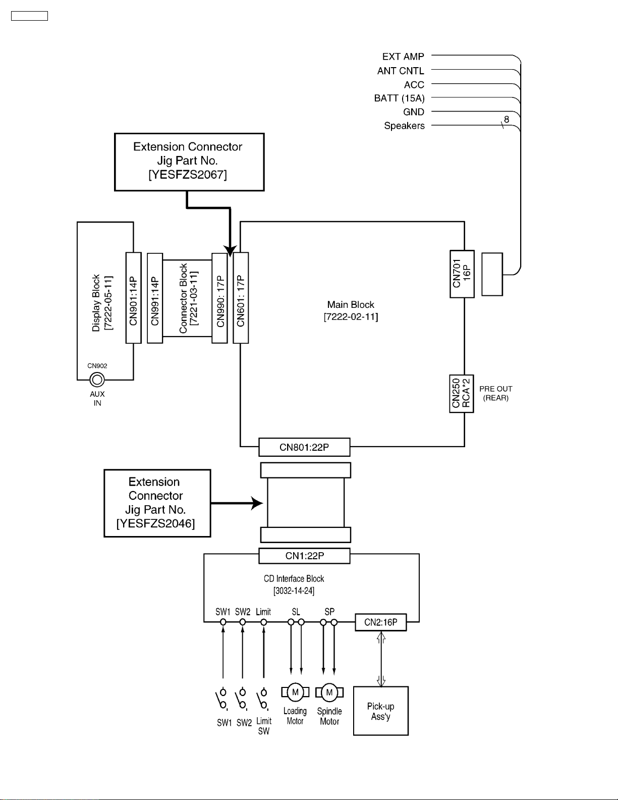
8 WIRING CONNECTION
4
9 TERMINALS DESCRIPTION
9.1. Main Block
IC601 : YESAM350
Pin
Port Description I/O (V)
No.
1 XIN Crystal oscillator I 2.5 2.5 2.5
2 TEST2 Ground I 0 0 0
3 VREG Bypass condenser
4 VSSCPU Ground - 0 0 0
5 NC - - - - 6 NC - - - - 7 NC - - - - 8 NC - - - - -
9 LCD DO LCD data output I 5 5 5
10 LCD DI LCD data input O 4.9 5 4.9
11 LCD CLK LCD clock O 5.1 5.1 5.1
12 LCD CE LCD chip enable output O 0 0 0.3
13 CD DO CD data output I 5.1 5.2 4
14 CD DI CD data input O 0 0 4.6
15 CD CLK CD clock O 4.9 49 4.9
16 CD CE CD chip enable O 0 0 1
17 CD LM
(+)
18 CD LM (-) CD loading motor control O 0 0 0
19 CD S/L CD spindle motor control O 5.1 5.1 5.1
20 SUB
READY
21 CD
INSW1
22 CD SW2 CD mechanism SW2 I 5.1 5.1 0
23 CD LIMITSWCD limit SW I 0.2 0.2 5.1
24 CD MUTE CD Mute signal I 5.1 5.1 5.1
25 CD RST CD reset O 5.1 5.1 5.1
26 CD
DMUTE
27 LOW
BATT
28 NC - - - - 29 PANEL Panel detect switch I 0 0 0
30 NC - - - - 31 NC - - - - 32 NC - - - - 33 NC - - - - 34 NC - - - - 35 NC - - - - 36 NC - - - - 37 NC - - - - 38 NC - - - - 39 VDD
PORT
40 VSS
PORT
41 NC - - - - 42 NC - - - - 43 NC - - - - 44 NC - - - - 45 NC - - - - 46 NC - - - - 47 NC - - - - 48 NC - - - - 49 PWR
CNT
50 AMP CNT Amp control signal O 5.1 5.1 5.1
51 AMP
MUTE
connected.
CD loading motor control O 0 0 0
Sub CPU ready signal I 0 0 5
CD insert SW input I 0 0 0
CD mute O 0 0 5.1
Battery low level detect I 5.1 5.1 0
Power supply (+5V) - 5.1 5.1 5.1
Ground - 0 0 0
Power on control O 4.9 5 5
Power IC mute signal O 5.1 5.1 5.1
FM AM CD
O 2.9 2.9 2.9
Pin
Port Description I/O (V)
No.
52 STBY Power IC standby control O 5.1 5.1 5.1
53 SSC Tuner search sensitivity
54 AF MUTE AF mute O 5.1 5.1 5.1
55 I2C DATA Electronic VOL data O 5.1 5.1 5.1
56 I2C CLK Electronic VOL clock O 5.1 5.1 5.1
57 ANT CNT Motor antenna drive
58 POWER
LED
59 NC - - - - 60 NC - - - - 61 NC - - - - 62 NC - - - - 63 OP/CL Panel open/close signal I - - 64 EJECT Eject switch signal I 5.1 5.1 5.1
65 EJ ILL Eject LED drive control O 5.1 5.1 5.1
66 TEL
MUTE
67 BATT Battery detection I 5.1 5.1 5.1
68 MODE B Rotary encoder input B I 5 5 5
69 NC - - - - 70 RM DATA Remote control data I - - 71 MODE A Rotary encoder input A I 5 5 5.1
72 NC - - - - 73 NC - - - - 74 NC - - - - 75 AM
MODE
76 FM
MODE
77 LEVEL Audio signal input for
78 INIT C Initial setting port I 0 0 0
79 INIT B Initial setting port I 0 0 0
80 INIT A Initial setting port I 0 0 0
81 VSSADC Ground - 0 0 0
82 NC - - - - 83 ST FM stereo signal I 5.1 5.2 5.2
84 SD
FM/AM
85 NC Ground I 0 0 0
86 RESET Reset signal I 5 5 5
87 ACC ACC signal input I 5.3 5.3 5.3
88 NC Ground I 0 0 0
89 NC Ground I 0 0 0
90 FM/AM
IFC
91 NC - - - - 92 NC - - - - 93 VDDPLL Power supply of PLL - 5.1 5.1 5.1
94 NC - - - - 95 OSC
FM/AM
96 VSSPLL Ground - 0 0 0
97 NC - - - - 98 EO1 PLL phase comparison
99 TEST1 Ground I 0 0 0
100 XOUT Crystal oscillator O 2.6 2.6 2.6
change
control
Power LED O 0 0 0
Telephone mute signal I 5.1 5.1 5.1
Radio AM mode control O 8.2 0 8.2
Radio FM mode control O 0 8.2 0
level meter
Radio signal strength I 0 0 0
FM/AM IF input I 1.4 1.3 1.3
FM/AM osc input I 1.4 1.3 1.3
error output
FM AM CD
O 0 0 5.1
O 5.1 5.1 5.1
I 0 0 1.5
O 2.2 2.1 2.3
CQ-C3303H
5
CQ-C3303H
9.2. Display Block
IC901 : YEAMLC75854T
Pin No. Port Description I/O (V)
1, 2 NC - - -
3-39 SEG3 -39 LCD segment data O 2.5
40 -43 COM1 -4 LCD common O 2.5
44, 45 SEG40, 41 LCD segment data O 2.5
46 -49 KS3-6 Key scan O 5.0
50 -54 Kl1-5 Key data I 0
55 TEST (Connecting to ground) - 0
56 VDD +5V power supply - 5.0
57 VDD1 VDD1 filter terminal - 3.3
58 VDD2 VDD2 filter terminal - 1.7
59 VSS Ground - 0
60 OSC Oscillator terminal - 3.8
61 DO Key data output O 5.0
62 CE LCD driver chip enable I 0.3
63 CLK LCD clock I 5.1
64 DI LCD data I 4.9
6
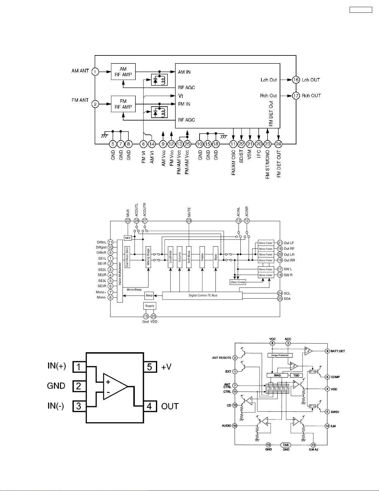
10 PACKAGE AND IC BLOCK DIAGRAM
10.1. Main Block
PA051 : YESAP403
CQ-C3303H
IC231 : YESAM320
IC201 : YESAM293
IC751 : YESAM349
7
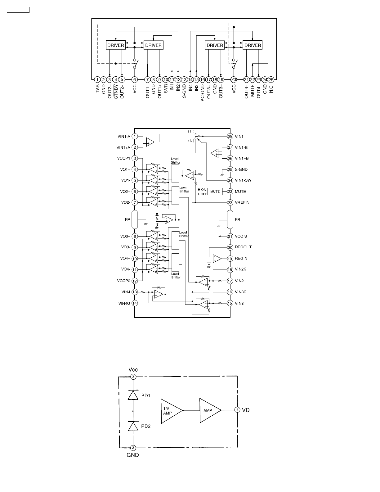
CQ-C3303H
IC271 : C1EA00000041
10.2. Display Block
IC802 : YESAM352
IC905 : YESAM264
8
11 REPLACEMENT PARTS
LIST
Notes :
1. Be sure to make your orders of replacement parts
according to this list.
2. Important safety notice: Components, identified by
have special characteristics important for safety. When
replacing any of these components, use only
manufacturer´s specified parts.
3. Location keys in the remarks column indicates the general
location of the parts shown in the exploded drawing, as in a
road map.
4. The marking (RTL) indicates that Retention Time is limited
for this item. After the discontinuation of assembly in
production, the item will continue to be available for a
specific period of time. The retention period of availability is
dependent on the type of assembly, and in accordance with
the laws governing part and product retention. After the end
of this period, the assembly will no longer be available.
•
• Order intake period is basically six months after the first
• •
shipment.
Ref. No. Part No. Part Name & Description Remarks
[7222-02-11] Main Block
IC´s and TRANSISTORs
IC201 YESAM293 IC
IC231 YESAM320 IC
IC271 C1EA00000041 IC
IC601 YESAM350 IC
IC751 YESAM349 IC
IC801 YESAM351 IC
IC802 YESAM352 IC
PA051 YESAP403 Tuner Pack
Q052 YESAN117 Transistor
Q055 YESAN117 Transistor
Q261 YESAN121 Transistor
Q262 YESAN121 Transistor
Q265 YESAN125 Transistor
Q361 YESAN121 Transistor
Q362 YESAN121 Transistor
Q365 YESAN125 Transistor
Q401 YEAN2SK536TB FET
Q660 YESAN128 Transistor
Q661 YESAN127 Transistor
Q671 YESAN120 Transistor
Q672 YESAN118 Transistor
Q701 YESAN126 Transistor
Q702 YESAN129 Transistor
Q703 YESAN123 Transistor
Q704 YESAN123 Transistor
Q751 YESAN115 FET
Q752 YESAN115 FET
Q770 YESAN087 Transistor
Q851 B1BCCF000017 Transistor
Q871 YESAN113 Transistor
DIODEs
D053 YESAD119 Zener Diode
D231 YESAD143 Diode
D232 YESAD144 Diode
D233 YESAD119 Zener Diode
D270 YESAD146 Diode
D271 YESAD146 Diode
D272 YESAD146 Diode
D273 YESAD146 Diode
D274 YESAD146 Diode
D275 YESAD146 Diode
mark
CQ-C3303H
Ref. No. Part No. Part Name & Description Remarks
D276 YESAD146 Diode
D277 YESAD146 Diode
D677 YESAD147 Zener Diode
D691 YESAD155 Diode
D701 YESAD139 Diode
D702 YESAD153 Zener Diode
D703 YESAD146 Diode
D704 YESAD143 Diode
D705 YESAD146 Diode
D751 YESAD141 Diode
D770 YESAD123 Zener Diode
D791 B0ACCK000005 Diode
D792 B0ACCK000005 Diode
CAPACITORs
C051 YECUS1H470JC Ceramic, 47pF 50WV
C053 YESCC482 Ceramic, 0.01µF 50WV
C055 YESCC482 Ceramic, 0.01µF 50WV
C058 YESCC482 Ceramic, 0.01µF 50WV
C065 YESCC481 Ceramic, 0.001µF 50WV
C067 YESCC482 Ceramic, 0.01µF 50WV
C071 YESCC559 Ceramic, 0.012µF 50WV
C61 YESCC527 Ceramic, 0.022µF 25WV
C62 YESCC527 Ceramic, 0.022µF 25WV
C201 YESCC529 Ceramic, 0.22µF 16WV
C202 YESCC550 Electrolytic, 3.3µF 50WV
C204 YESCC452 Ceramic, 1µF 16WV
C206 YESCC549 Electrolytic, 2.2µF 50WV
C207 YESCC452 Ceramic, 1µF 16WV
C208 YESCC483 Ceramic, 0.1µF 50WV
C231 YESCC483 Ceramic, 0.1µF 50WV
C232 YESCC483 Ceramic, 0.1µF 50WV
C233 YESCC481 Ceramic, 0.001µF 50WV
C234 YESCC563 Ceramic, 2.2µF
C235 YESCC545 Electrolytic, 22µF 10WV
C236 YESCC563 Ceramic, 2.2µF
C251 YESCC226 Ceramic, 470pF 50WV
C261 YESCC372 Electrolytic, 4.7µF 25WV
C262 YESCC372 Electrolytic, 4.7µF 25WV
C263 YESCC487 Ceramic, 0.47µF 16WV
C267 YESCC487 Ceramic, 0.47µF 16WV
C268 YESCC487 Ceramic, 0.47µF 16WV
C269 YESCC487 Ceramic, 0.47µF 16WV
C271 YESCC486 Ceramic, 0.0047µF 50WV
C272 YESCC486 Ceramic, 0.0047µF 50WV
C276 YESCC548 Electrolytic, 47µF 16WV
C277 YESCC452 Ceramic, 1µF 16WV
C278 YESCC483 Ceramic, 0.1µF 50WV
C279 YESCC368 Electrolytic, 2200µF 16WV
C280 YESCC563 Ceramic, 2.2µF
C281 YESCC563 Ceramic, 2.2µF
C301 YESCC529 Ceramic, 0.22µF 16WV
C302 YESCC550 Electrolytic, 3.3µF 50WV
C304 YESCC452 Ceramic, 1µF 16WV
C306 YESCC549 Electrolytic, 2.2µF 50WV
C307 YESCC546 Electrolytic, 10µF 16WV
C308 YESCC539 Electrolytic, 120µF 10WV
C351 YESCC226 Ceramic, 470pF 50WV
C361 YESCC372 Electrolytic, 4.7µF 25WV
C362 YESCC372 Electrolytic, 4.7µF 25WV
C363 YESCC487 Ceramic, 0.47µF 16WV
C367 YESCC487 Ceramic, 0.47µF 16WV
C368 YESCC487 Ceramic, 0.47µF 16WV
C369 YESCC487 Ceramic, 0.47µF 16WV
C371 YESCC486 Ceramic, 0.0047µF 50WV
C372 YESCC486 Ceramic, 0.0047µF 50WV
C375 YESCC404 Electrolytic, 10µF 16WV
C378 YESCC483 Ceramic, 0.1µF 50WV
C401 YESCC543 Electrolytic, 680µF 10WV
C402 ECQV1H683JL2 Plastic, 0.068µF 50WV
C403 YESCC562 Ceramic, 0.0068µF 50WV
C404 YESCC482 Ceramic, 0.01µF 50WV
C421 F1J1H101A667 Ceramic, 100pF 50WV
9
 Loading...