

Panasonic CQC-3302-N Service manual
Specifications*
ORDER NO. ACED060611C3
AUTOMOTIVE AFTERMARKET
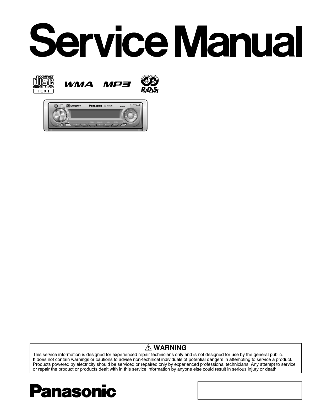
CQ-C3302N
WMA MP3 CD Player/Receiver
General
Power Supply DC 12V (11V - 16V),
Test Voltage 14.4V
Negative Ground
Current Consumption Less than 2.2A (CD mode ; 0.5W
4-channels)
Maximum Power Output 50W×4 (at 4Ω)
Power Output 22Wx4 (DIN45 324, at 4Ω)
Tone Adjustment Range Bass ; ±12dB at 100Hz
Treble ; ±12dB at 10kHz
Speaker Impedance 4-8Ω
Pre-Amp Output Voltage 2.5V (CD mode)
Pre-Amp Output Impedance 200Ω
FM Stereo Radio
Frequency Range 87.5MHz - 108MHz
Usable Sensitivity 6dB/µV (S/N 30dB)
Stereo Separation 35db (at 1kHz)
AM (MW) Radio
Frequency Range 531kHz - 1,602kHz
Usable Sensitivity 27dB/µV (S/N 20dB)
AM (LW) Radio
Frequency Range 153kHz - 279kHz
Usable Sensitivity 32dB/µV (S/N 20dB)
CD Player
Sampling Frequency 8 Times Oversampling
DA Converter 1bit DAC System
Pick-Up Type Astigma 3-beam
Light Source Semiconductor Laser
Wave Length 790nm
Frequency Response 20Hz to 20kHz (±1dB)
Signal to Noise Ratio 96dB
Total Harmonic Distortion 0.01% (1kHz)
Wow and Flutter Below measurable limits
Channel Separation 75dB
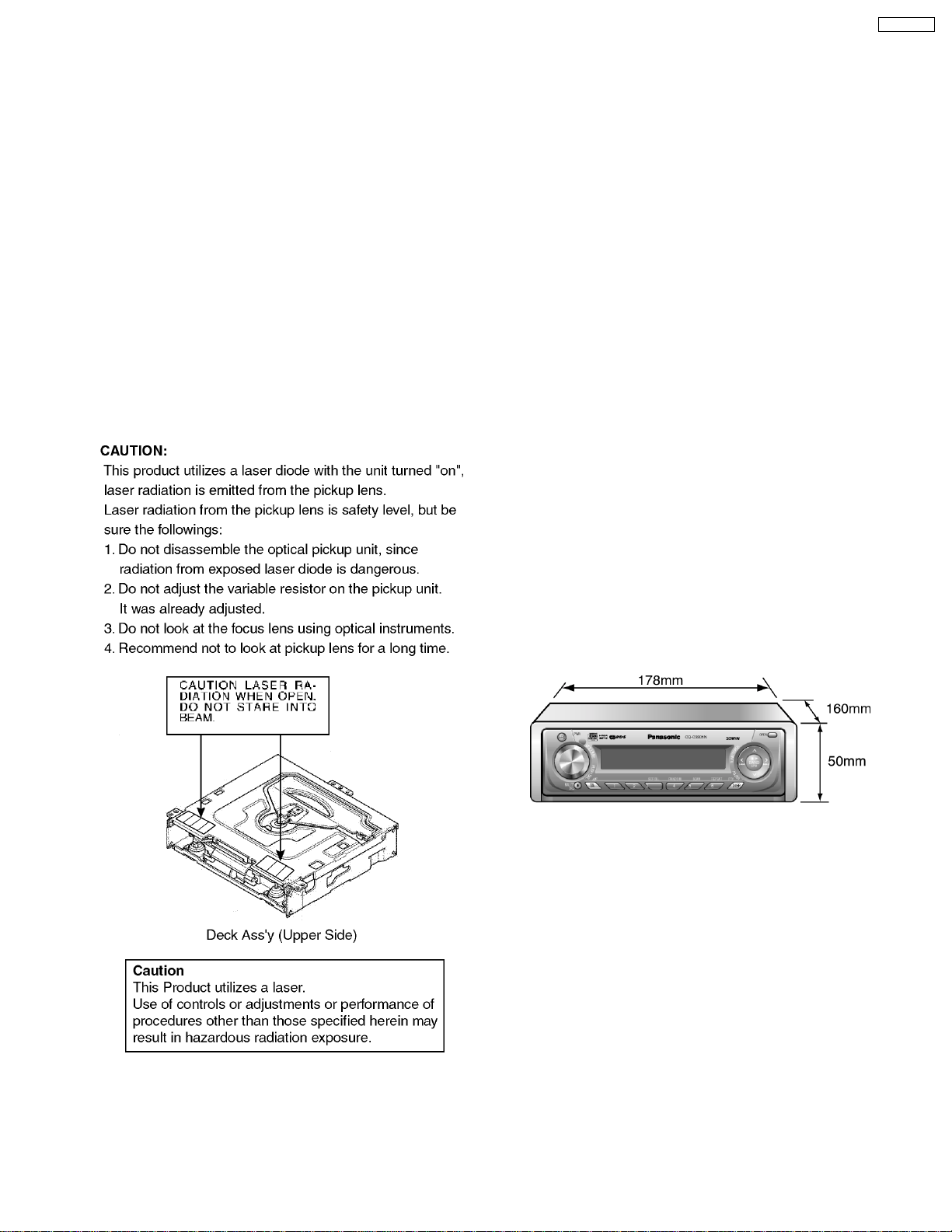
Dimensions** 178×50×160mm
Weight** 1.4kg
* Specifications and the design are subject to possible modification
without notice due to improvements.
** Dimensions and Weight shown are approximate.
•
• Above specifications comply with EIA standards.
• •
© 2006 Matsushita Electric Industrial Co., Ltd. All
rights reserved. Unauthorized copying and
distribution is a violation of law.
CQ-C3302 N
CONTENTS
Page Page
1 ABOUT LEAD FREE SOLDER (PbF) 3
2 LASER PRODUCTS
3 FEATUERS
4 REPLACING THE FUSE
5 MAINTENANCE
6 NOTES
7 DIMENSIONS
8 WIRING CONNECTION
9 TERMINALS DESCRIPTION
10 PACKAGE AND IC BLOCK DIAGRAM
11 REPLACEMENT PARTS LIST
3
3
12 EXPLODED VIEW (Unit)
3
13 CD PLAYER PARTS LIST
14 EXPLODED VIEW (CD Deck)
3
3
15 WIRING DIAGRAM
3
16 SCHEMATIC DIAGRAM -1
17 SCHEMATIC DIAGRAM -2
4
5
18 BLOCK DIAGRAM
8
11
15
16
19
20
26
27
31
2
CQ-C3302 N
1 ABOUT LEAD FREE
SOLDER (PbF)
Distinction of PbF PCB:
PCBs (manufactured) using lead free solder will have a PbF
stamp on the PCB.
Caution :
•
•
Pb free solder has a higher melting point than standard
• •
solder; Typically the melting point is 50 - 70°F (30 40°C) higher. Please use a soldering iron with
temperature control and adjust it to 700 ± 20°F (370 ±
10°C). In case of using high temperature soldering iron,
please be careful not to heat too long.
•
•
Pb free solder will tend to splash when heated too high
• •
(about 1100°F/600°C)
•
•
This lead free solder will be used for the products after
• •
serial No. 1,000,001.
2 LASER PRODUCTS
3 FEATUERS
•
•
Digital servo for reliable playback.
• •
•
•
PLL (Phase Locked Loop) synthesized tuning.
• •
•
•
18-FM, 6-AM presets with preset scan.
• •
•
•
Removable face plate.
• •
•
•
MP3/WMA Playback from CD-R/RW.
• •
4 REPLACING THE FUSE
Use fuses of the same specified rating (15amps). Using
different substitutes or fuses with higher ratings, or connecting
the product directly without a fuse, could cause fire or damage
to the stereo unit.
5 MAINTENANCE
Your product is designed and manufactured to ensure a
minimum of maintenance. Use a dry, a soft cloth for routine
exterior cleanin g. Never use benzine, thinner or other solvents.
6 NOTES
[RADIO BLOCK]
Do not align the AM/FM package block. When the package
block is necessary, it will be supplie d already aligned at the
factory.
[CD DECK BLOCK]
This model has no servo alignment points because
microcomputer controls the servo circuit.
7 DIMENSIONS
3
CQ-C3302 N
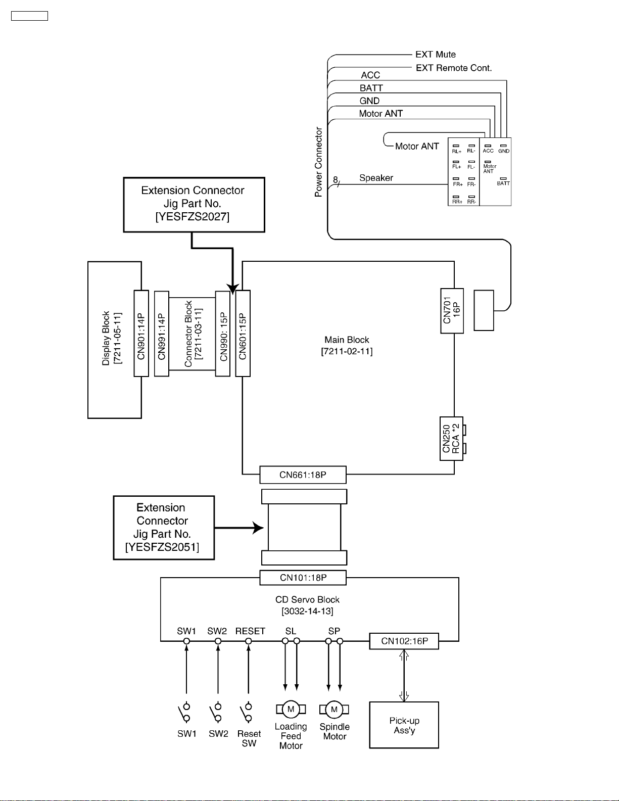
8 WIRING CONNECTION
4
9 TERMINALS DESCRIPTION
CQ-C3302 N
9.1. Main Block
IC601 : YESAM285
Pin
No.
1 (NC) - - - - 2 VSM Radio signal strength I 0 0 0
3 SD/ST Radio station detect I 0.3 0 0.8
4 AVSS Ground - 0 0 0
5 SCL Audio control serial clock O 4.9 4.9 4.9
6 SDA Audio control data O 4.9 4.9 4.9
7 AVREF (Conecting to +5V) - 4.9 4.9 4.9
8 CD SO CD data output I 2.1 2.3 1.7
9 CD SI CD data input O 0 0 3.3
10 CD SCK CD clock O 4.7 4.7 4.7
11 CDC DATA/
12 XM-RX SI XM radio RX signal O 4.8 4.8 4.8
13 CDC CLK CD changer clock I 0 0 0
14 CDC REM CD changer remote O 4.8 4.8 4.8
15 BZ OUT Buzzer out O 4.4 4.4 4.4
16 LCD DO LCD data I 4.8 4.8 4.8
17 LCD DI LCD data O 4.7 4.7 4.7
18 LCD CLK LCD Clock O 4.8 4.8 4.8
19 CD AO CD mute I 0 0 4.8
20 CD RST CD reset O 4.8 4.8 4.8
21 CD STB CD strobe I 3.7 3.7 3.7
22 CDC SENS
23 PLL DO PLL data I 4.9 4.9 4.9
24 PLL CLK PLL data clock O 4.8 4.8 4.8
25 PLL DI PLL data O 0 0 0
26 PLL CE PLL chip select O 0 0 0
27 (NC) - - - - 28 (NC) - - - - 29 (NC) - - - - 30 (NC) - - - - 31 (NC) - - - - 32 (NC) - - - - 33 VSS1 Ground - 0 0 0
34 RDS DATA RDS data I 2.8 0 0
35 S-LED LED control O 0 0 0
36 LCD CE LCD chip enable O 0 0 0
37 LCD 5V CNT Display 5V control O 0 0 0
38 EJ ILL LED control (EJ/ILL) O 4.8 4.8 4.8
39 OP/CL Panel open/close detect I 4.9 4.9 4.9
40 (NC) - - - - 41 EJECT EJECT switch I 4.9 4.9 4.9
42 ROTARY 1 Rotary encoder input 1 I 4.8 4.8 4.8
43 ROTARY 2 Rotary encoder input 2 I 4.7 4.7 4.7
44 (NC) - - - - 45 (NC) - - - - 46 PANEL Panel detection I 4.6 4.6 4.6
47 STBY Power IC stundby control O 4.8 4.8 4.8
48 EEPROM CE (Not Used) - - - 49 EEPROM SK
50 EEPROM DI
51 EEPROM DO (Not Used) - - - 52 CDC1/2 (NC) - - - - 53 INV CNT Illumination control O 4.8 4.8 4.8
54 AMP CNT Amp power control O 4.8 4.8 4.8
55 ANT CNT Antenna power control O 4.8 4.8 4.8
56 EXT.MUTE External mute O 4.8 4.8 4.8
57 MAIN CNT Main power control O 4.8 4.8 4.8
Port Description I/O (V)
XM-TX SO
(NC)
(NC)
(NC)
CD changer data/XM
radio TX signal
- - - - -
- - - - -
- - - - -
FM AM CD
I 0 0 0
Pin
No.
58 AMP MUTE Amp mute control O 4.8 4.8 4.8
59 AF MUTE AF mute control O 4.8 4.8 4.8
60 RESET Reset I 4.8 4.8 4.8
61 RDS CLK RDS clock I 2.8 2.8 2.8
62 (NC) - - - - 63 (NC) - - - - 64 RM DATA Remote control data I 4.8 4.8 4.8
65 BATT Battery voltage detection I 4.5 4.5 4.5
66 CDC STB/
67 VSS0 Ground - 0 0 0
68 VDD1 +5V power supply - 4.8 4.8 4.8
69 X2 Crystal oscillator - 2.9 2.9 2.9
70 X1 Crystal oscillator - 2.3 2.3 2.3
71 TEST (TEST terminal) - 0 0 0
72 XT2 Crystal oscillator - 2.7 2.7 2.7
73 XT1 Crystal oscillator - 2 2 2
74 VDD0 +5V power supply - 4.9 4.9 4.9
75 AVDD +5V power supply - 4.8 4.8 4.8
76 INI A Mode setting A I 0 0 0
77 INI B Mode setting B I 4.8 4.8 4.8
78 ACC ACC detection I 4.9 4.9 4.9
79 (NC) (Connecting to ground) - 0 0 0
80 LEVEL Audio signal I 0 0 0
Port Description I/O (V)
XM DET
CD Changer strobe/ XM
receiver detection
FM AM CD
I 4.8 4.8 4.8
9.2. Display Block
IC901 : YEAMLC75854T
Pin
No.
1-16 SEG1-16 LCD segment data O 2.5
17-39 SEG19-41 LCD segment data O 2.5
40-43 COM1-4 LCD common O 2.5
44,45 SEG17,18 LCD segement data O 2.5
46-49 KS3-6 Key scan O 5.0
50-54 Kl1-5 Key data I 0
55 TEST (Connecting to ground) - 0
56 VDD +5V power supply - 5.0
57 VDD1 VDD1 filter terminal - 3.3
58 VDD2 VDD2 filter terminal - 1.7
59 VSS Ground - 0
60 OSC Oscillator terminal - 3.9
61 DO Key data output O 5.0
62 CE LCD driver chip enable I 0
63 CLK LCD clock I 4.9
64 DI LCD data I 4.9
Port Description I/O (V)
5
CQ-C3302 N
9.3. CD Servo Block
IC401 : YESAM348
Pin
No.
Port Descriptions I/O (V)
1 CVSS1 GND - 0
2 - - - 3 CVSS2 GND - 0
4 DVDD1 I/O system (3.3V) power supply - 3.3
5 A10 Address bus of FLASH ROM O 0
6 - - - 7 A11 Address bus of FLASH ROM O 3.3
8 A12 O 3.3
9 A13 O 3.3
10 A14 O 3.3
11 A15 O 3.3
12 /CVDD1 CORE CPU system (1.6V) power
supply
13 - - - 14 DVSS1 GND - 0
15 CVSS3 GND - 0
16 /CVDD2 I/O system (3.3V) power supply - 1.6
17 - - - 18 - - - 19 READY - - 3.3
20 /PS FLASH ROM selection signal O 3.3
21 - - - 22 - - - 23 R/W Lead/light signal to FLASH ROM O 3.3
24 /MSTRB Memory access signal O 3.3
25 - - - 26 /MSC - - 3.3
27 MUTE Mute signal output (H:Mute on) O 0
28 - - - 29 - - - 30 /HOLD - - 3.3
31 BIO SUBO input I 0
32 MP/MC Operation mode setting (external pull-
up)
33 DVDD2 I/O system (3.3V) power supply - 3.3
34 CVSS4 GND - 0
35 BD R1 GND I 0
36 - - - 37 CVSS5 GND - 0
38 - - - 39 - - - 40 DVSS2 GND - 0
41 CLK C M AUDIO bit clock input I 1.6
42 SCK Clock input I 3.3
43 LRCK CMAUDIO L/R identifying signal input I 1.6
44 CDFS Serial frame sink signal input I 2.6
45 DATACMAUDIO serial data input I 1.6
46 - - - 47 SI Serial data input I 0
48 CLK M C AUDIO bit clock output O 1.6
49 SCK Clock input I 3.3
50 CVSS6 GND - 0
51 - - - 52 CVDD3 CORE CPU system (1.6V) power
supply
53 LRCK MCAUDIO L/R identifying signal output O 1.6
54 CDFS Serial frame sink signal input I 2.4
55 - - - 56 DVDD3 I/O system (3.3V) power supply - 3.3
57 DVSS3 GND - 0
- 1.6
I 3.3
- 1.6
Pin
No.
100 D1 I/O 0
101 D2 I/O 0
102 D3 I/O 0
103 D4 I/O 0
104 D5 I/O 0
105 A16 Address bus of FLASH ROM O 0
106 DVSS7 GND - 0
107 A17 Address bus of FLASH ROM O 3.3
108 A18 O 0
109 A19 Address bus of FLASH ROM O 0
110 A20 O 0
111 CVSS9 GND - 0
112 DVDD5 I/O system (3.3V) power supply - 3.3
113 D6 Data bus of FLASH ROM I/O 0
114 D7 I/O 0
115 D8 I/O 0
116 D9 I/O 0
117 D10 I/O 0
Port Descriptions I/O (V)
58 RESTSWMechanics deck REST SW input I 3.3
59 DATA MCAUDIO serial data output O 1.6
60 SO Serial data output O 1.2
61 - - - 62 - - - 63 /NMI - - 3.3
64 /INT0 - - 3.3
65 /INT1 - - 3.3
66 BLKCK Subcode block clock pulse input I 0
67 /INT3 - - 3.3
68 CV DD4 CORE CPU system (1.6V) power
69 SW1 Mechanics deck SW1 input I 0
70 CVSS7 GND - 0
71 MCLK Clock output (To Servo DSP) O 3.3
72 DVSS4 GND - 0
73 MLD Command load signal output (To
74 MDATA Command data output (To Servo
75 DVDD4 I/O system (3.3V) power supply - 3.3
76 DVSS5 GND - 0
77 CLK MD1 Clock mode setting (L fixation) I 0
78 CLK MD2 Clock mode setting (H fixation) I 3.3
79 CLK MD3 Clock mode setting (L fixation) I 80 - - - 81 SW2 Mechanics deck SW2 input I 0
82 - - - 83 EMU0 - - 0
84 EMU/OF
F
85 TDO - - 3.3
86 TDI - - 0
87 /TRST - - 3.3
88 TCK - - 0
89 TMS - - 3.3
90 CVSS8 GND - 3.3
91 CVDD5 CORE CPU system (1.6V) power
92 HPIENA GND I 1.6
93 DVSS6 GND - 0
94 - - - 95 CLKENA Oscillation output Cainabl signal O 3.3
96 X1 Crystal Connection O 0
97 X2/CLKIN Crystal Connection I 0
98 RS Reset signal input I 1
99 D0 Data base of FLASH ROM I/O 3.4
supply
Servo DSP)
DSP)
- - 3.3
supply
- 1.6
I 3.3
O 3.3
- 0
6
Pin
Port Descriptions I/O (V)
No.
118 D11 Data bus of FLASH ROM I/O 0
119 D12 I/O 0
120 STAT Status signal input I 0.4
121 D13 Data path of FLASH ROM I/O 0
122 D14 I/O 0
123 D15 I/O 0
124 - - - 125 CVDD6 CORE CPU system (1.6V) power
- 1.6
supply
126 CVSS10 GND - 0
127 - - - 128 DVSS8 I/O system (3.3V) power supply - 0
129 - - - 130 DVDD6 I/O system (3.3V) power supply - 3.3
131 A0 Address bus of FLASH ROM O 0
132 A1 O 0
133 A2 O 3.3
134 A3 O 3.3
135 /RST Reset signal output (To Servo DSP) O 3.3
136 A4 Address bus of FLASH ROM O 3.3
137 A5 O 0
138 A6 O 3.3
139 A7 O 3.3
140 A8 O 0
141 A9 O 3.3
142 CVDD7 CORE CPU system (1.6V) power
- 1.6
supply
143 - - - 144 DVSS9 GND - 0
CQ-C3302 N
7
CQ-C3302 N
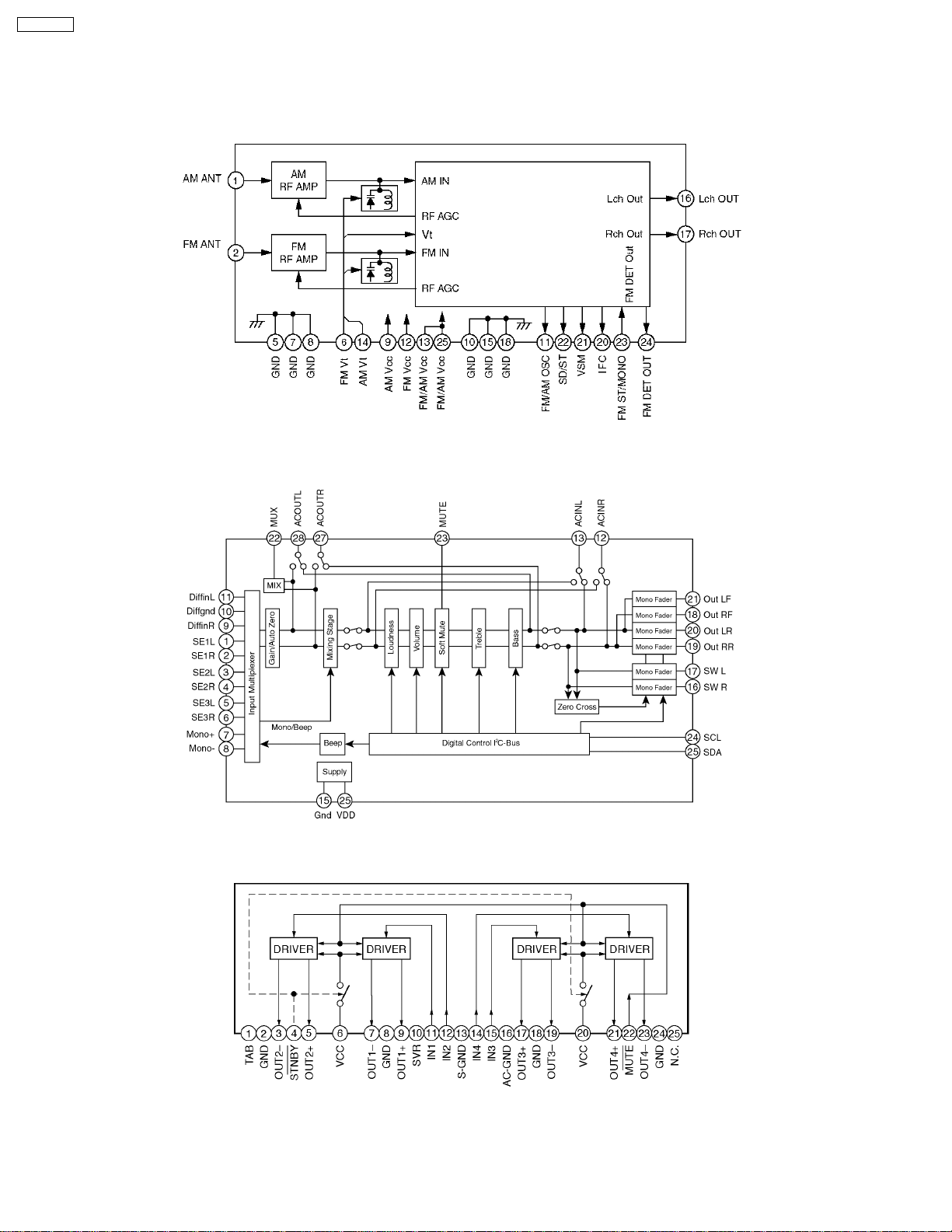
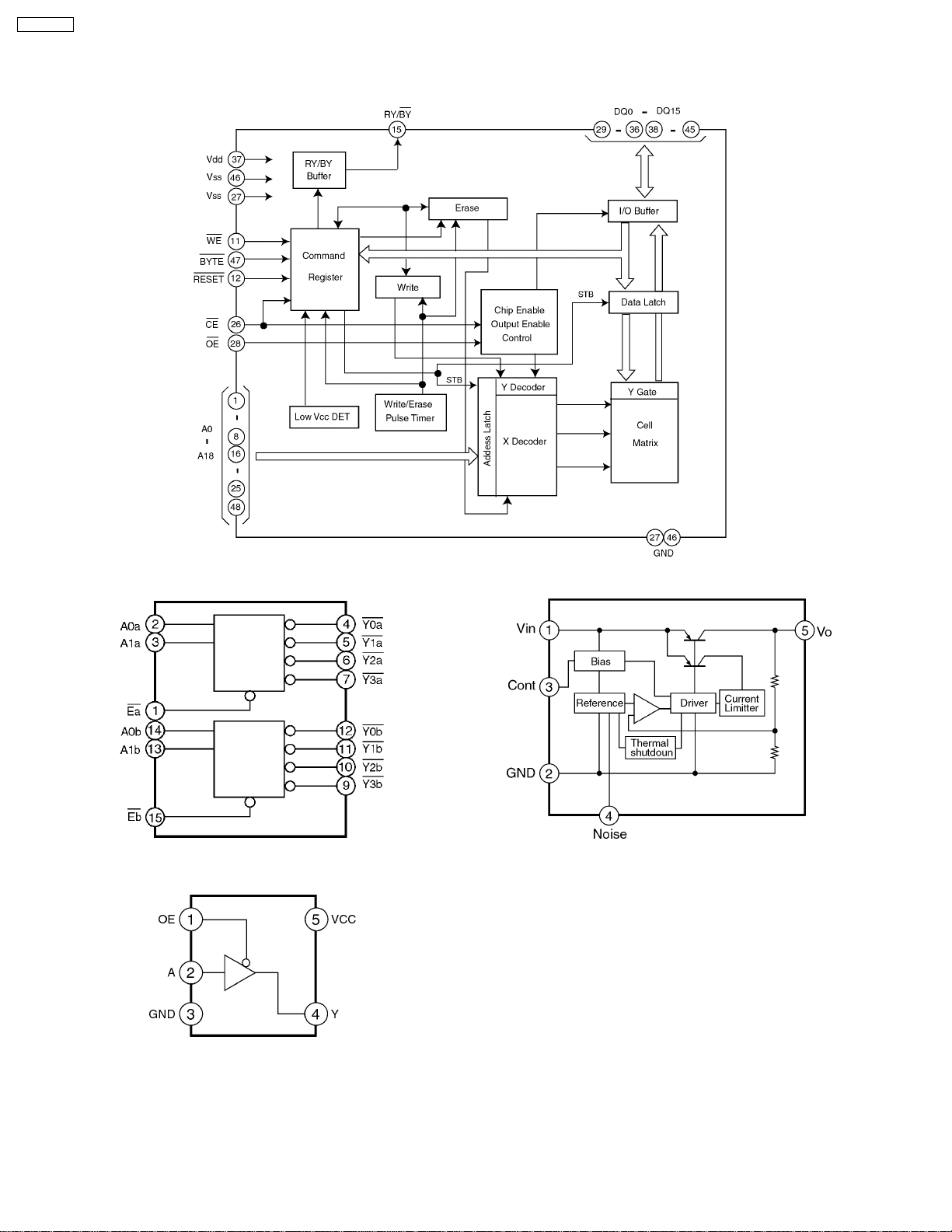
10 PACKAGE AND IC BLOCK DIAGRAM
10.1. Main Block
PA051 : YESAP403
IC201 : C1BB00000543
IC271 : C1EA00000041
8
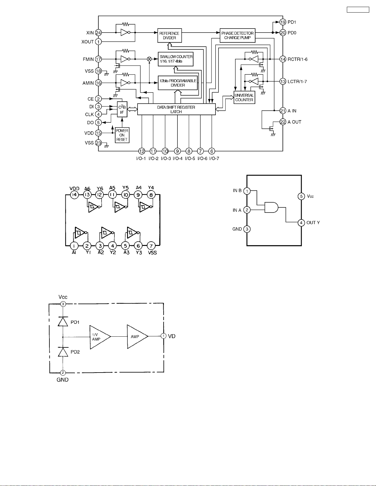
IC401 : YESAM284
CQ-C3302 N
IC650 : YESAM265
10.2. Display Block
IC905 : YESAM264
IC681 : YESAM273
9
CQ-C3302 N
10.3. CD Servo Block
IC403 : YESAM171
IC402 : YESAM353
IC404 : YESAM178
IC405 : YESAM270
10
11 REPLACEMENT PARTS
LIST
Notes :
1. Be sure to make your orders of replacement parts
according to this list.
2. Important safety notice: Components, identified by
have special characteristics important for safety. When
replacing any of these components, use only
manufacturer´s specified parts.
3. Location keys in the remarks column indicates the general
location of the parts shown in the explod ed drawing, as in a
road map.
4. The marking (RTL) indicates that Retention Time is limited
for this item. After the discontinuation of assembly in
production, the item will continue to be available for a
specific period of time. The retention period of availability is
dependent on the type of assembly, and in accordance with
the laws governing part and product retention. After the end
of this period, the assembly will no longer be available.
•
•
Order intake period is basically six months after the first
• •
shipment.
Ref. No. Part No. Part Name & Description Remarks
[7211-02-11] Main Block
IC´s and TRANSISTORs
IC201 C1BB00000543 IC
IC231 C0ABBB000038 IC
IC271 C1EA00000041 IC
IC401 YESAM284 IC
IC501 YESAM283 IC
IC601 YESAM285 IC
IC650 YESAM265 IC
IC681 YESAM273 IC
IC710 YESAM277 IC
IC740 YESAM269 IC
IC750 YESAM267 IC
IC755 YESAM263 IC
PA051 YESAP403 Tuner Pack
Q052 YESAN082 Transistor
Q054 B1GBCFNN0009 Transistor
Q055 YESAN082 Transistor
Q066 YESAN091 Transistor
Q262 YESAN085 Transistor
Q266 YESAN085 Transistor
Q362 YESAN085 Transistor
Q366 YESAN085 Transistor
Q411 YEAN2SK536TB FET
Q660 YESAN081 Transistor
Q661 YESAN080 Transistor
Q670 B1GBCFNN0009 Transistor
Q671 B1GDCFJJ0008 Transistor
Q672 YESAN092 Transistor
Q681 YESAN084 Transistor
Q720 YESAN093 FET
Q721 YESAN084 Transistor
Q730 YESAN093 FET
Q731 YESAN084 Transistor
Q740 YESAN079 Transistor
Q751 YESAN087 Transistor
Q761 YESAN090 Transistor
Q770 YESAN088 Transistor
DIODEs
D051 YESAD143 Diode
D052 YESAD143 Diode
D201 YESAD133 Zener Diode
D270 YESAD146 Diode
mark
CQ-C3302 N
Ref. No. Part No. Part Name & Description Remarks
D271 YESAD146 Diode
D272 YESAD146 Diode
D273 YESAD146 Diode
D274 YESAD146 Diode
D275 YESAD146 Diode
D276 YESAD146 Diode
D277 YESAD146 Diode
D601 YESAD143 Diode
D602 YESAD133 Zener Diode
D603 YESAD133 Zener Diode
D604 YESAD133 Zener Diode
D605 YESAD133 Zener Diode
D606 YESAD133 Zener Diode
D607 YESAD133 Zener Diode
D608 YESAD133 Zener Diode
D610 YESAD143 Diode
D636 YESAD144 Diode
D637 YESAD143 Diode
D638 YESAD119 Zener Diode
D670 YESAD148 LED
D681 YESAD149 Diode
D701 YESAD139 Diode
D702 YESAD119 Zener Diode
D710 YESAD144 Diode
D720 YESAD146 Diode
D740 YESAD146 Diode
D741 YESAD118 Diode
D750 YESAD141 Diode
D760 YESAD146 Diode
D761 YESAD140 Diode
D770 YESAD123 Zener Diode
D790 YESAD143 Diode
CAPACITORs
C051 YECUS1H470JC Ceramic, 47pF 50WV
C053 YESCC234 Ceramic, 0.01µF 50WV
C055 YESCC234 Ceramic, 0.01µF 50WV
C061 YESCC327 Ceramic, 0.018µF 50WV
C062 YESCC327 Ceramic, 0.018µF 50WV
C065 YESCC233 Ceramic, 0.001µF 50WV
C066 YESCC226 Ceramic, 470pF 50WV
C067 YESCC234 Ceramic, 0.01µF 50WV
C203 YESCC314 Electrolytic, 3.3µF 50WV
C208 YESCC230 Ceramic, 0.33µF 16WV
C210 YESCC228 Ceramic, 0.1µF 16WV
C220 YESCC375 Electrolytic, 2.2µF 50WV
C234 YESCC228 Ceramic, 0.1µF 16WV
C235 YESCC284 Ceramic, 0.18µF 50WV
C237 YESCC319 Ceramic, 0.082µF 50WV
C238 YESCC392 Electrolytic, 22µF 10WV
C240 YESCC228 Ceramic, 0.1µF 16WV
C261 YESCC372 Electrolytic, 4.7µF 25WV
C263 YECUS1C474KX Ceramic, 0.47µF 16WV
C265 YESCC372 Electrolytic, 4.7µF 25WV
C267 YECUS1C474KX Ceramic, 0.47µF 16WV
C268 YECUS1C474KX Ceramic, 0.47µF 16WV
C269 YECUS1C474KX Ceramic, 0.47µF 16WV
C271 YESCC235 Ceramic, 0.0047µF 50WV
C272 YESCC235 Ceramic, 0.0047µF 50WV
C276 YESCC393 Electrolytic, 47µF 16WV
C277 YESCC229 Ceramic, 1µF 16WV
C278 YESCC228 Ceramic, 0.1µF 16WV
C279 YESCC368 Electrolytic, 2200µF 16WV
C280 YESCC191 Ceramic, 2.2µF 50WV
C281 YESCC191 Ceramic, 2.2µF 50WV
C292 YESCC234 Ceramic, 0.01µF 50WV
C303 YESCC314 Electrolytic, 3.3µF 50WV
C308 YESCC230 Ceramic, 0.33µF 16WV
C309 YESCC333 Electrolytic, 100µF 16WV
C310 YESCC313 Electrolytic, 220µF 10WV
C320 YESCC375 Electrolytic, 2.2µF 50WV
C325 YECUS1H104KX Ceramic, 0.1µF 50WV
C339 YESCC231 Ceramic, 0.022µF 25WV
11
CQ-C3302 N
Ref. No. Part No. Part Name & Description Remarks
C361 YESCC372 Electrolytic, 4.7µF 25WV
C363 YECUS1C474KX Ceramic, 0.47µF 16WV
C365 YESCC372 Electrolytic, 4.7µF 25WV
C367 YECUS1C474KX Ceramic, 0.47µF 16WV
C368 YECUS1C474KX Ceramic, 0.47µF 16WV
C369 YECUS1C474KX Ceramic, 0.47µF 16WV
C371 YESCC235 Ceramic, 0.0047µF 50WV
C372 YESCC235 Ceramic, 0.0047µF 50WV
C378 YESCC228 Ceramic, 0.1µF 16WV
C401 YESCC219 Ceramic, 10pF 50WV
C402 YESCC245 Ceramic, 12pF 50WV
C403 YESCC376 Electrolytic, 100µF 6.3WV
C404 YESCC234 Ceramic, 0.01µF 50WV
C405 F1J1H101A025 Ceramic, 100pF 50WV
C411 YESCC234 Ceramic, 0.01µF 50WV
C412 YESCC344 Ceramic, 0.015µF 50WV
C413 ECQV1H104JL2 Plastic Film, 0.1µF 50WV
C417 YESCC371 Electrolytic, 680µF 16WV
C421 F1J1H101A025 Ceramic, 100pF 50WV
C430 YESCC313 Electrolytic, 220µF 10WV
C501 YESCC223 Ceramic, 27pF 50WV
C502 YESCC219 Ceramic, 10pF 50WV
C505 YESCC375 Electrolytic, 2.2µF 50WV
C506 YESCC244 Ceramic, 0.01µF 50WV
C507 YESCC224 Ceramic, 270pF 50WV
C508 YESCC366 Electrolytic, 10µF 16WV
C509 YESCC392 Electrolytic, 22uF 10WV
C602 YESCC378 Electrolytic, 1000µF 6.3WV
C605 YESCC234 Ceramic, 0.01µF 50WV
C628 YESCC228 Ceramic, 0.1µF 16WV
C629 YESCC228 Ceramic, 0.1µF 16WV
C631 YESCC229 Ceramic, 1µF 16WV
C632 YESCC377 Electrolytic, 47µF 6.3WV
C634 YECUS1H220JC Ceramic, 22pF 50WV
C635 YECUS1H220JC Ceramic, 22pF 50WV
C636 YESCC191 Ceramic, 2.2µF 50WV
C637 YESCC233 Ceramic, 0.001µF 50WV
C638 YESCC191 Ceramic, 2.2µF 50WV
C660 YESCC375 Electrolytic, 2.2µF 50WV
C670 YESCC234 Ceramic, 0.01µF 50WV
C672 YESCC394 Electrolytic, 4.7uF 50WV
C681 YECUS1H104KX Ceramic, 0.1µF 50WV
C682 YECUS1H104KX Ceramic, 0.1µF 50WV
C683 YECUS1H104KX Ceramic, 0.1µF 50WV
C701 YESCC374 Electrolytic, 1µF 50WV
C710 YESCC284 Ceramic, 0.18µF 50WV
C711 YESCC234 Ceramic, 0.01µF 50WV
C740 YESCC369 Electrolytic, 470µF 16WV
C741 YESCC379 Electrolytic, 150µF 6.3WV
C751 YESCC370 Electrolytic, 1000µF 16WV
C752 YESCC365 Electrolytic, 120µF 10WV
C753 YESCC377 Electrolytic, 47µF 6.3WV
C755 YESCC228 Ceramic, 0.1µF 16WV
C756 YESCC380 Electrolytic, 39µF 6.3WV
C757 YECUS1H104KX Ceramic, 0.1µF 50WV
C770 YESCC367 Electrolytic, 100µF 16WV
C790 YESCC228 Ceramic, 0.1µF 16WV
RESISTORs
J712 YESRG204 Carbon, 560Ω1/4W
J714 YESRG204 Carbon, 560Ω1/4W
J801-829 YESRG132 Chip, 0Ω1/4W
J830 ERJ8GX0R00V Chip, 0Ω1/4W
J831 YESRG132 Chip, 0Ω1/4W
J832 YESRG132 Chip, 0Ω1/4W
J833 YESRG132 Chip, 0Ω1/4W
J834 YESRG132 Chip, 0Ω1/4W
J836 YESRG132 Chip, 0Ω1/4W
J838 YESRG132 Chip, 0Ω1/4W
J839 YESRG132 Chip, 0Ω1/4W
J839 ERJ8GX0R00V Chip, 0Ω1/4W
J901 YESRG093 Chip, 0Ω1/8W
J902 YESRG093 Chip, 0Ω1/8W
Ref. No. Part No. Part Name & Description Remarks
J903 YESRG093 Chip, 0Ω1/8W
J905 YESRG093 Chip, 0Ω1/8W
J906 YESRG093 Chip, 0Ω1/8W
J907 YESRG093 Chip, 0Ω1/8W
J908 YESRG093 Chip, 0Ω1/8W
J909 YESRG093 Chip, 0Ω1/8W
J910 YESRG093 Chip, 0Ω1/8W
J911 YESRG093 Chip, 0Ω1/8W
J912 YESRG093 Chip, 0Ω1/8W
L291 YESRG093 Chip, 0Ω1/8W
R050 YESRG127 Chip, 5.6Ω1/8W
R051 YESRG132 Chip, 0Ω1/4W
R052 YESRG094 Chip, 100Ω1/8W
R052 YESRG094 Chip, 100Ω1/8W
R053 YESRG246 Chip, 120Ω1/8W
R058 YESRG093 Chip, 0Ω1/8W
R059 YESRG097 Chip, 100kΩ1/8W
R060 YESRG115 Chip, 33kΩ1/8W
R065 YESRG117 Chip, 3.9kΩ1/8W
R066 YESRG182 Chip, 330kΩ1/10W
R067 YESRG108 Chip, 2.2kΩ1/8W
R068 YESRG095 Chip, 1kΩ1/8W
R202 YESRG184 Chip, 4.3kΩ1/8W
R203 YESRG115 Chip, 33kΩ1/8W
R208 YESRG105 Chip, 18kΩ1/8W
R225 YESRG205 Carbon, 1kΩ1/4W
R226 YESRG205 Carbon, 1kΩ1/4W
R235 YESRG093 Chip, 0Ω1/8W
R237 YESRG096 Chip, 10kΩ1/8W
R238 YESRG115 Chip, 33kΩ1/8W
R239 YESRG097 Chip, 100kΩ1/8W
R261 YESRG138 Chip, 180Ω1/4W
R262 YESRG096 Chip, 10kΩ1/8W
R263 YESRG124 Chip, 560Ω1/8W
R265 YESRG103 Chip, 180Ω1/8W
R266 YESRG135 Chip, 10kΩ1/4W
R267 YESRG124 Chip, 560Ω1/8W
R275 YESRG109 Chip, 22kΩ1/8W
R280 YESRG212 Chip, 130Ω1/8W
R291 YESRG093 Chip, 0Ω1/8W
R302 YESRG184 Chip, 4.3kΩ1/8W
R303 YESRG115 Chip, 33kΩ1/8W
R308 YESRG105 Chip, 18kΩ1/8W
R325 YESRG096 Chip, 10kΩ1/8W
R326 YESRG096 Chip, 10kΩ1/8W
R338 YESRG148 Chip, 47kΩ1/4W
R361 YESRG103 Chip, 180Ω1/8W
R362 YESRG096 Chip, 10kΩ1/8W
R363 YESRG124 Chip, 560Ω1/8W
R365 YESRG103 Chip, 180Ω1/8W
R366 YESRG135 Chip, 10kΩ1/4W
R367 YESRG124 Chip, 560Ω1/8W
R375 YESRG137 Chip, 12kΩ1/4W
R391 YESRG093 Chip, 0Ω1/8W
R401 YESRG154 Chip, 10Ω1/4W
R402 YESRG124 Chip, 560Ω1/8W
R403 YESRG100 Chip, 1.5kΩ1/8W
R404 YESRG093 Chip, 0Ω1/8W
R405 YESRG206 Carbon, 2.2kΩ1/4W
R406 YESRG208 Carbon, 47kΩ1/4W
R407 YESRG104 Chip, 1.8kΩ1/8W
R408 YESRG108 Chip, 2.2kΩ1/8W
R409 YESRG108 Chip, 2.2kΩ1/8W
R410 YESRG108 Chip, 2.2kΩ1/8W
R411 YESRG108 Chip, 2.2kΩ1/8W
R412 YESRG119 Chip, 4.7kΩ1/8W
R413 YESRG120 Chip, 47kΩ1/8W
R416 YESRG108 Chip, 2.2kΩ1/8W
R417 YESRG189 Chip, 100Ω1/4W
R501 YESRG180 Chip, 2.2MΩ1/10W
R506 YESRG096 Chip, 10kΩ1/8W
R601 YESRG147 Chip, 4.7kΩ1/4W
R602 YESRG134 Chip, 1kΩ1/4W
R603 YESRG120 Chip, 47kΩ1/8W
12
 Loading...