

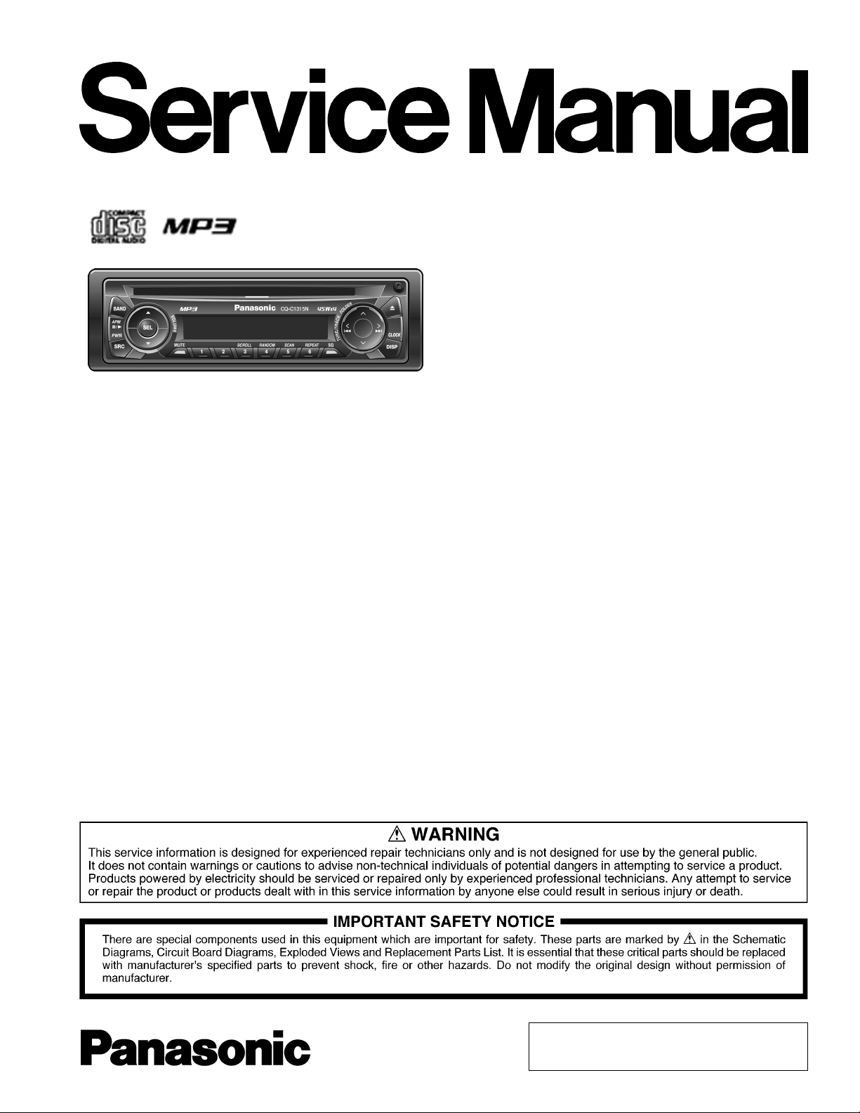
Panasonic CQC-1315-N Service manual
Specifications*
Order No. ACED061203C8
AUTOMOTIVE AFTERMARKET
CQ-C1315N
Removable Front Panel CD Player /
Receiver
General
Power Supply DC 12V (11V - 16V),
Test Voltage 14.4V
Negative Ground
Tone Controls Bass ; ±12dB at 100Hz
Treble ; ±12dB at 10kHz
Current Consumption Less than 2.2A (CD play mode,
0.5W×4ch)
Maximum Power Output 45W×4ch (at 1kHz, Vol. Max.)
Suitable Speaker Impedance 4-8Ω
FM Stereo Radio
Frequency Range 87.5 - 108MHz
Usable Sensitivity 11.0dBf (1.25µV, 75Ω)
AM Radio
Frequency Range 531 - 1,602kHz
Usable Sensitivity 28dB/µV (25µV, S/N 20dB)
CD Player
Sampling Frequency 8 times oversampling
Pick-Up Type Astigma 3-beam
Light Source Semiconductor Laser
Wavelength 780nm
Frequency Response 20Hz to 20,000Hz (±1dB)
Signal to Noise Ratio 96dB
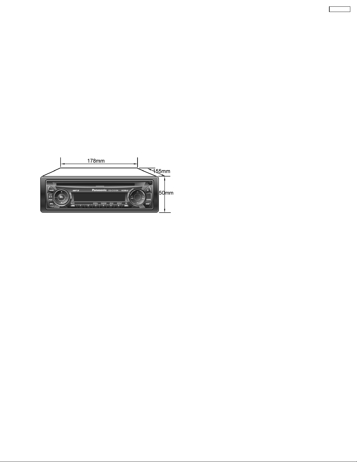
Dimensions** 178×50×155mm
Weight** 1.4kg
* Specifications and the design are subject to possible modification
without notice due to improvements.
** Dimensions and Weight shown are approximate.
© 2006 Matsushita Electric Industrial Co., Ltd. All
rights reserved. Unauthorized copying and
distribution is a violation of law.
CQ-C1315N
CONTENTS
Page Page
1 ABOUT LEAD FREE SOLDER (PbF) 2
2 FEATUERS
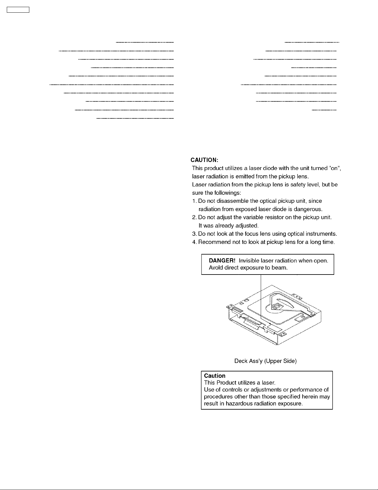
3 LASER PRODUCTS
4 REPLACEING THE FUSE
5 MAINTENANCE
6 NOTES
7 DIMENSIONS
8 WIRING CONNECTION
9 BLOCK DIAGRAM
10 TERMINALS DESCRIPTI ON
11 PACKAGE AND IC BLOCK DIAGRAM 9
2
12 REPLACEMENT PARTS LIST
13 EXPLODED VIEW (Unit)
2
2
14 CD PLAYER MECHANICAL PARTS LIST
15 EXPLODED VIEW (CD Deck)
3
3
16 WIRING DIAGRAM
3
17 SCHEMATIC DIAGRAM-1
18 SCHEMATIC DIAGRAM-2
4
5
19 SCHEMATIC DIAGRAM for printing with A4 size
6
12
16
17
18
19
23
25
27
1 ABOUT LEAD FREE
SOLDER (PbF)
Distinction of PbF PCB:
PCBs (manufactured) using lead free solder will have a PbF
stamp on the PCB.
Caution :
•
• Pb free solder has a higher melting point than standard
• •
solder; Typically the melting point is 50 - 70°F (30 40°C) higher. Please use a soldering iron with
temperature control and adjust it to 700 ± 20°F (370 ±
10°C). In case of using high temperature soldering iron,
please be careful not to heat too long.
•
• Pb free solder will tend to splash when heated too high
• •
(about 1100°F/600°C)
•
• This lead free solder will be used for the products after
• •
serial No. 1,000,001.
2 FEATUERS
•
• Remote Control.
• •
•
• 18-FM, 6-AM presets with preset scan
• •
•
• Digital servo for reliable CD playback.
• •
•
• Removable face plate.
• •
3 LASER PRODUCTS
4 REPLACEING THE FUSE
Use fuses of the same specified rating (15A). Using different
substitutes or fuses with higher ratings, or connecting the
product directly without a fuse, could cause fire or damage to
the stereo unit.
2
5 MAINTENANCE
Your products is designed and manufactured to ensure a
minimum of maintenance. Use a dry, a soft cloth for routine
exterior cleaning. Never use benzine, thinner or other solvents.
6 NOTES
[RADIO BLOCK]
Do not align the AM/FM package block. When the package
block is necessary, it will be supplied already aligned at the
factory.
[CD DECK BLOCK]
This model has no servo alignment points because
microcomputer controls the servo circuit.
7 DIMENSIONS
CQ-C1315N
3
CQ-C1315N
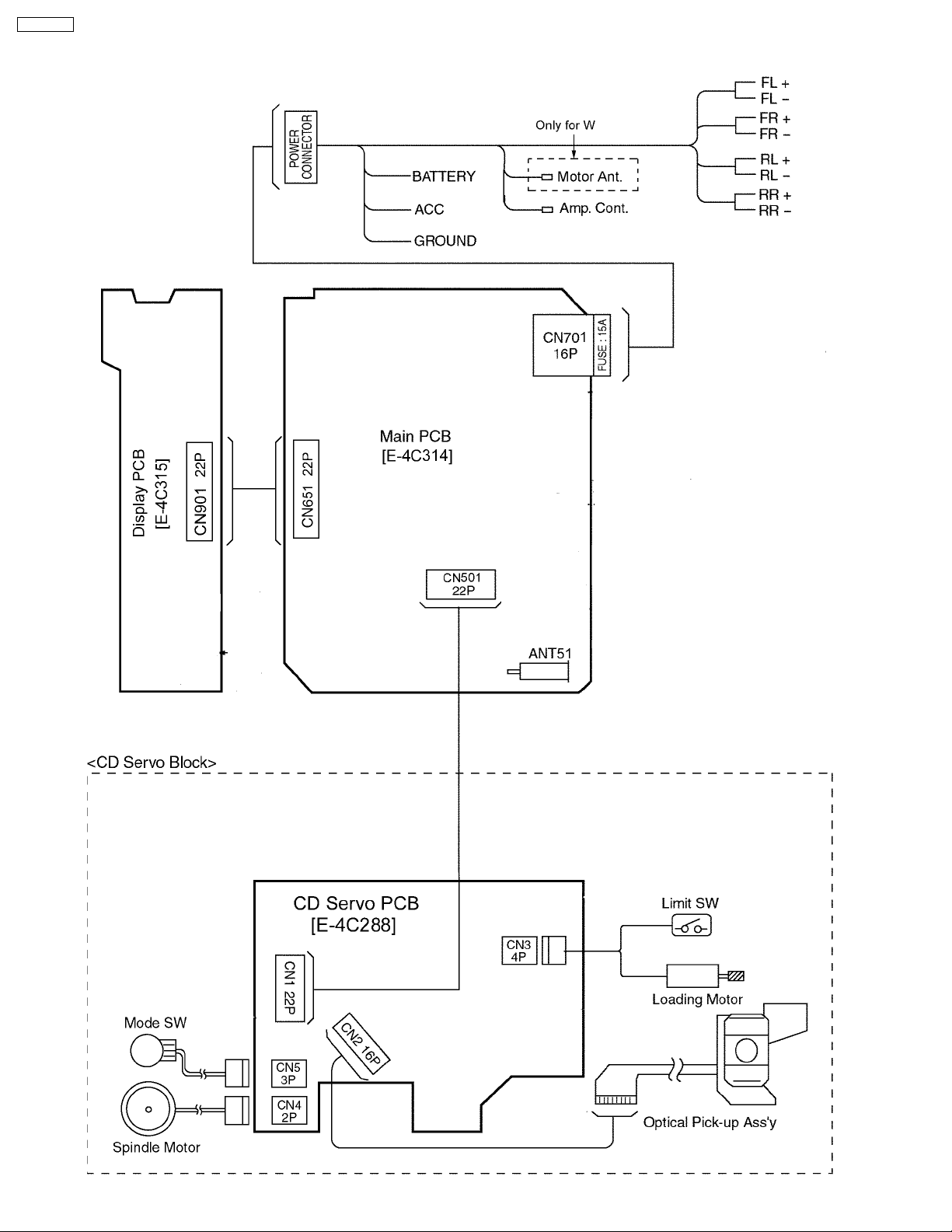
8 WIRING CONNECTION
4
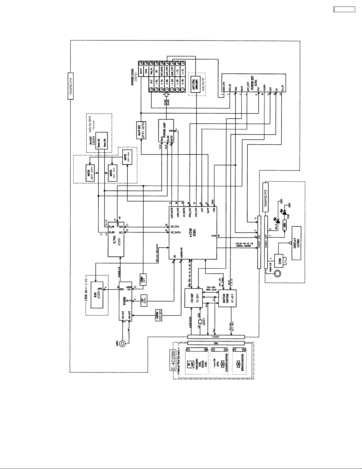
9 BLOCK DIAGRAM
CQ-C1315N
5
CQ-C1315N
10 TERMINALS DESCRIPTION
10.1. Main Block
IC601 : LC7237829D42
Ref.
Part No. Part Name &
No.
1 XIN 4. 5 MHz X’tal and
2 TEST2 GND connection I 0 0 0
3 VREG Bypass condenser
4 VSSCPU GND connection - 0 0 0
5 CDC_DATA CD changer data I 0 0 0
6 N.C. None - - - 7 CDC_CLK CD changer clock I 0 0 0
8 CDC_REM_OUT CD changer Remote out O 0 0 0
9 LCD_DO LCD data output I 5.2 5.21 5.21
10 LCD_DI LCD data input O 5.01 5.04 5.01
11 LCD_CLK LCD clock O 5.14 5.16 5.16
12 LCD_CE LCD chip enable output O 0.17 0.17 0.17
13 CD_DO CD data output I 5.36 5.38 3.9
14 CD_DI CD data input O 0 0 4.74
15 CD_CLK CD clock O 4.96 4.98 4.96
16 CD_CE CD chip enable O 0 0 1.57
17 CD_LM+ CD eject O 0 0 0
18 CD_LM- CD loading O 0 0 0
19 CD_S/L CD 24PIN connection O 0 0 5.19
20 SUB_RDY CD INTB1 connection I 0.12 0.1 5.22
21 CD_INSW1 CD insert SW input I 0.1 0.1 0.1
22 CD_SW2 CD MECHA SW2 I 5.15 5.7 0.1
23 CD_LIMIT_SW CD limit SW I 0 0 5.17
24 CD_DRF CD Mute I 5.33 5.35 5.35
25 CD_RST CD reset O 0 0 5.13
26 CD_BATT CD_BATT O 0 0 5.18
27 N.C. None O 5.17 5.19 5.19
28 N.C. None - - - 29 PANEL Panel detect I 5.21 5.22 5.22
30 N.C. GND connection I 0 0 0
31 N.C. GND connection I 0 0 0
32 N.C. GND connection I 0 0 0
33 N.C. None - - - 34 N.C. None - - - 35 N.C. None - - - 36 N.C. None - - - 37 N.C. None - - - 38 N.C. None - - - 39 VDDPORT Power supply of PORT - 5.17 5.19 5.19
40 VSSPORT GND of PORT - 0 0 0
41 N.C. None - - - 42 N.C. None - - - 43 N.C. None - - - 44 N.C. None - - - 45 N.C. None - - - 46 N.C. None - - - 47 N.C. None - - - 48 N.C. None - - - 49 PWR_CNT Power control O 5.15 5.17 5.17
50 AMP_CNT Amp stand-by O 5.15 5.17 5.17
51 AMP_MUTE Amp mute O 5.17 5.19 5.19
52 N.C. None - - - 53 SSC Tuner search
54 AF_MUTE AF mute O 5.17 5.19 5.19
55 I2C_DATA Electronic VOL data O 5.17 5.19 5.19
56 I2C_CLK Electronic VOL clock O 5.17 5.19 5.19
57 ANT_CNT Motor antena control O 5.17 5.19 0
58 POWER_LED Power LED O 0.15 0.16 0.13
59 N.C. None - - - 60 N.C. (
BZ_OUT )
61 N.C. None - - - 62 N.C. None - - - 63 N.C. None - - - -
Description
Connection
connected.
sensitivity change
None - - - -
I/O FM(V)AM(V)CD(V
I 2.52 2.54 2.53
O 2.94 2.95 2.95
O 0 0 0
Ref.
No.
)
64 N.C. None - - - 65 N.C. None - - - 66 TEL_MUTE External MUTE input I 0 0 0
67 BATT Battery detection I 5.19 5.2 5.2
68 MODE_B ROTARY B input I 5.1 5.17 5.17
69 RDS_CLK RDS clock I 0 0 0
70 REM_IN Remocon data input I 5.12 5.14 5.12
71 MODE_A ROTARY A input I 5.16 5.17 5.16
72 CDC_STB CD changer strobe
73 NC None - - - 74 MONO Compulsion MONO ON O 0 0 0
75 AM_MODE AM change O 8.19 0.13 8.24
76 FM_MODE FM change O 0.13 8.18 8.24
77 N.C. GND connection I 0 0 0
78 INIT_C Initial value C I 0 0 0
79 INIT_B Initial value B I 5.15 5.17 5.17
80 INIT_A Initial value A I 1.93 1.94 1.94
81 VSSADC GND connection - 0 0 0
82 RDS_DATA RDS data I 0 0 0
83 ST FM stereo input I 5.37 5.38 5.39
84 SD_FM/AM Signal detection I 3.3 3.28 0
85 N.C. GND connection I 0 0 0
86 RESET Reset Input I 5.2(
87 ACC Power supply I 5.4 5.4 5.41
88 N.C. GND connection I 0 0 0
89 N.C. GND connection I 0 0 0
90 FM/AM_IFC FM/AM IF input I 1.46 1.47 0
91 N.C. GND connection I 0 0 0
92 SUBPD None O 0 0 0
93 VDDPLL Power supply of PLL - 5.18 5.19 5.2
94 N.C. GND connection I 0 0 0
95 OSC_FM/AM FM/AM osc input I 1.46 1.39 0
96 VSSPLL GND connection - 0 0 0
97 N.C. None - - - 98 EO1 PLL phase comparison
99 TEST1 GND connection I 0 0 0
100 XOUT 4. 5 MHz X’tal and
Note 1 :
Voltage measuerments are with respect to ground, with a
voltmeter (internal resistance : 10M ohms).
IC501:YEAMLC78691N
Ref.
No.
1 EFMIN RF signal input port. I 1.58
2 RFOUT RF signal output port. O 1.67
3 LPF LPF capacitor connection port
4 PHLPF LPF capacitor connection port
5 AIN A signal input port. I 1.66
6 CIN C signal input port. I 1.66
7 BIN B signal input port. I 1.66
8 DIN D signal input port. I 1.66
9 FEC LPF capacitor connection port
10 RFMON LSI build-in analog signal
11 VREF VREF voltage output port. O 1.66
12 JITTC Capacitor connection port for
Part No. Part Name &
Part No. Part Name & Description I/O (V)
Description
input
error output
Connection
for RF signal DC level
detection.
for detection.
for FE signal.
monitor port.
JIT detection.
I/O FM(V)AM(V)CD(V
I 0 0 0
5.2(
PWR
PWR
OFF)
OFF)
O 1.93 2.02 0
O 2.62 2.63 2.63
O 1.64
O 1.68
O 1.6
O 1.64
O 0
)
5.2(
EJEC
T)
6
Ref.
Part No. Part Name & Description I/O (V)
No.
13 EIN E signal input port. I 1.65
14 FIN F signal input port. I 1.66
15 TEC LPF capacitor connection port
16 TE TE signal output port. O 1.57
17 TEIN TE signal input port for TES. I 1.65
18 LDD Laser power control output
19 LDS Laser power detection input
20 AVSS GND for analog. - 0
21 AVDD VDD for analog. - 3.27
22 FDO Focus control signal output
23 TDO Tracking control signal output
24 SLDO Thread control signal output
25 SPDO Spindle control signal output
26 VVSS1 GND for build-in VCO. - 0
27 PDOUT1 Phase comparison output port1
28 PDOUT0 Phase comparison output port0
29 PCKIST PDOUT0 1 output port for
30 VVDD1 VDD for VCO. - 3.29
31 DMUTEB DMUTEB (general) output port. - 32 PUIN PUIN (general) I/O port. (With
33 DEFFCT Detection signal output port. O 0
34 FSEQ Synchronous signal output port.
35 C2F C2 error signal output port. O 0
36 DVDD VDD for Digital. - 3.29
37 DVSS GND forDigital. - 0
38 DVDD18 VDD capacitor connection port
39 MONI0 Monitor port0. O 0
40 MONI1 Monitor port1. O 0
41 DVDD VDD for Digital. - 3.25
42 DVSS GND forDigital. - 0
43 CE Host IF: Communication enable
44 CL Host IF: Data transfer clock
45 DI Host IF: Data input port. I 0
46 DO Host IF: Data output port (Nch
47 RESB Reset input port. Make it L”
48 INTB Interrupt signal output port.
49 SUB_READY0 For host u-com IF: SUB-RDY
50 CD_MUTEO General I/O port2. (With built-
51 LOW_BATI General I/O port1 I/O 5.16
52 CONT General I/O port0 I/O 0
53 OSCCNT OSCOFF control port . Connected
54 STREQ Stream data demand signal
55 STCK Clock input port for stream
56 STDATA Stream data input port. I/O 0
57 TEST1 Inputport for test. Needed
58 DATA Lch/Rch data output port. - 59 DATACK Clock output port. - 60 LRSY Lch/Rch clock output port - -
for TE signal.
port.
port.
port. D/A output.
port. D/A output.
port. D/A output.
port. D/A output.
for build-in VCO control.
for build-in VCO control.
current setting.
built-in Pull-Up resistance.
Turning off when reset)
It becomes ¡§H” when
Synchronous Idle detected from
the EFM signal is corresponding
to Synchronous Idle of internal
generation.
for digital circuit.
signal input port.
input port.
output) Pull-Up is necessary.
when power ON.
(Servo)
output. (Nch and Pull-Up
resistance is necessary)
in Pull-Up resistance. Turning
off when reset)
with 0V when Reset.
output port.
data.
connect with 0V1
O 1.57
O 3.27
I 0
O 1.65
O 1.65
O 1.64
O 1.64
O 0
O 0
I 1.07
I/O 0
O 0
O 1.83
I 0
I 3.56
O 5.32
I 0
- -
O 0
I/O 5.31
I 0
I/O 0
I/O 0
I 0
Ref.
Part No. Part Name & Description I/O (V)
No.
61 VVDD2 VDD for build-in VCO. - 3.25
62 VPREF2 Built-in VCO oscillation
63 VCOC2 Built-in VCO control voltage
64 VPDOUT2 Output port for built-in VCO
65 VVSS2 GNDfor building VCO. Needed
66 DVDD18 VDD capacitor connection port
67 DVSS GND for Digital system. Needed
68 DVDD VDD for Digital system. - 3.25
69 DOUT Digital OUT output port. EIAJ
70 AMUTEB AMUTEB (general) output port. - 71 XVSS GND for oscillation circuit.
72 XOUT Connected of 16.9344MHz
73 XIN Connected of 16.9345MHz
74 XVDD VDD forOscillation circuit. - 3.19
75 LCHO L channel output port. O 0
76 LRVDD VDD for LR channel. - 3.21
77 LRVSS GND for LR channel. Needed
78 RCHO R channel output port. O 0
79 AVDD VDD for analog . - 3.27
80 SLCO Slice level control output
cooking stove setting input
terminal.
setting input port.
control.
connect with 0V.
for digital circuit.
connect with 0V.
format.
Needed connect with 0V.
oscillation.
oscillation.
connect with 0V.
port.
I 3.25
I 1.08
O 0.08
- 0
O 1.84
- 0
- -
- 0
O 1.39
I 1.35
- 0
O 1.6
CQ-C1315N
7
CQ-C1315N
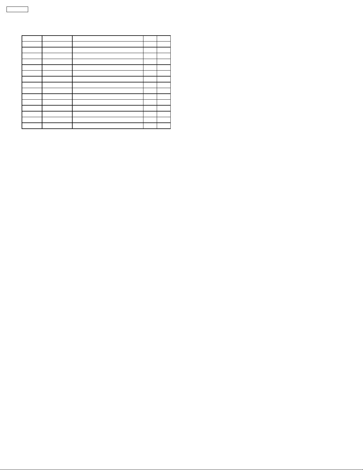
10.2. Display Block
IC901 : C0HBA0000223
Pin No. Port Descriptions I/O (V)
1-35 S1-35 LCD segment O 2.5
36-39 NC No connection - 40-43 C1-4 LCD common O 2.5
44-49 KS1-6 Key data output O 0.9
50-54 KI1-5 Key data input I 0
55 TEST (Connecting to ground) - 0
56 VDD +5V power supply - 5.1
57 VDD1 Ground through capacitor - 3.3
58 VDD2 Ground through capacitor - 1.7
59 Vss Ground - 0
60 OSC CR oscillator - 3.9
61 DO Key data output O 4.4
62 CE Chip enable I 0
63 CLK LCD clock I 0
64 DI LCD data input I 0
8
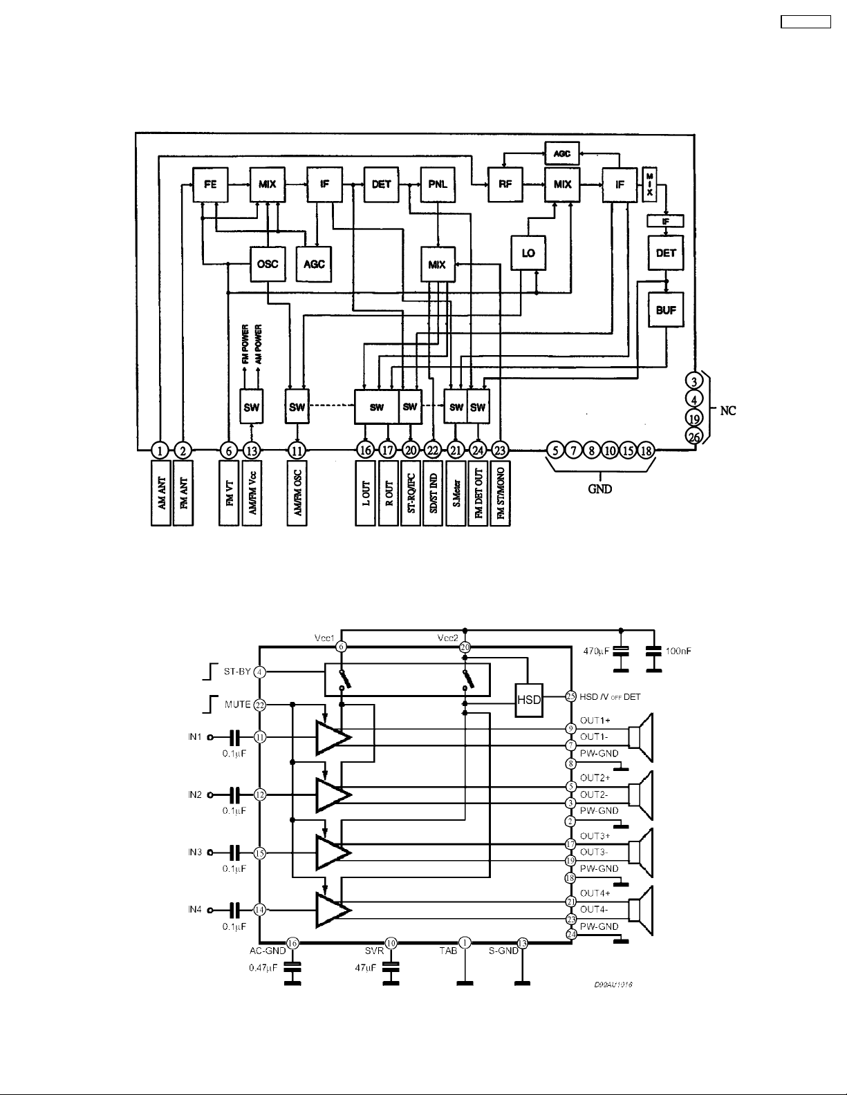
11 PACKAGE AND IC BLOCK DIAGRAM
11.1. Main Block
CQ-C1315N
PA51:J3CCBC000010
IC271 : C1EA00000042
9
 Loading...