

Panasonic CQC-1110-AN, CQC-1110-GN, CQC-1110-VN, CQC-1120-AN, CQC-1120-GN Service manual
Specifications*
ORDER NO. ACED040125C8
AUTOMOTIVE AFTERMARKET
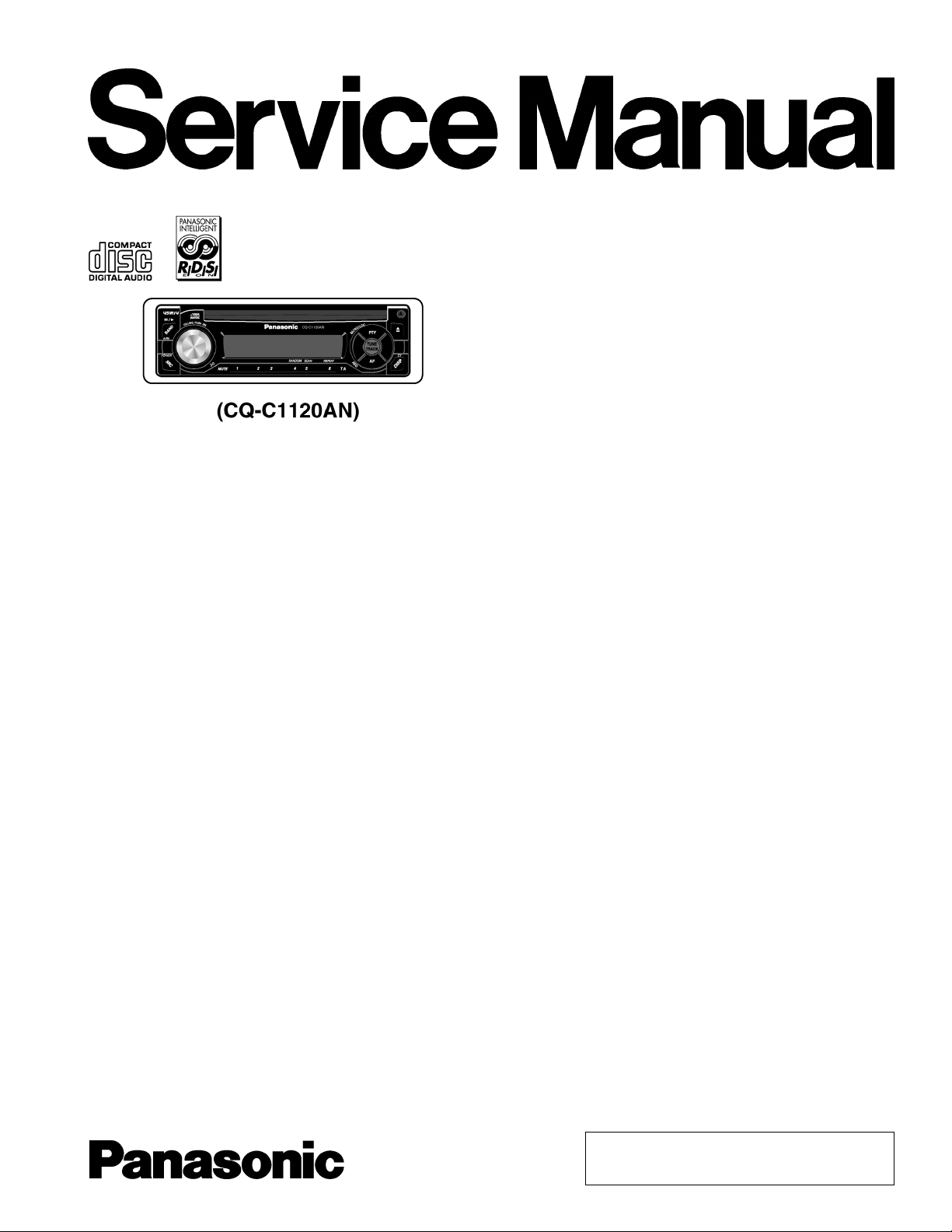
CQ-C1120AN
CQ-C1120GN
CQ-C1110AN
CQ-C1110GN
CQ-C1100VN
CD Player/Receiver
General
Power Supply 12V DC(11V-16V),
Test Voltage 14.4V
Negative Ground
Tone Control (Bass) ±12dB at 100Hz
Tone Control (Treble) ±12dB at 10Hz
Current Consumption Less than 2.5A
(CD mode; 0.5W × 4-speaker)
Maximum Power Output 45W × 4 (at 4Ω)
Power Output 20W × 4 (DIN45 324, at 4Ω)
Speaker Impedance 4-8Ω
Pre-amp Output Voltage 2.5V (CD mode)
Pre-amp Output Impedance 200Ω
CD Player
Sampling Frequency 8 Times Oversampling
Pick-up Type Astigma 3-Beam
Light Source Semiconductor Laser
Wave Length 780 nm
Frequency Response 20 Hz-20kHz (±1dB)
Signal to Noise Ratio 96dB
Total Harmonic Distortion 0.01% (1kHz)
Wow and Flutter Below Measurable Limits
Channel Separation 75dB
Radio
FM
Frequency Range 87.5MHz - 108MHz
Usable Sensitivity 6dB/µV(S/N 30dB)
Stereo Separation 35dB (at 1kHz)
MW
Frequency Range 531kHz - 1,602kHz
Usable Sensitivity 28dB/µV (S/N 20dB)
LW
Frequency Range 153kHz - 279kHz
Usable Sensitivity 32dB/µV (S/N 20dB)
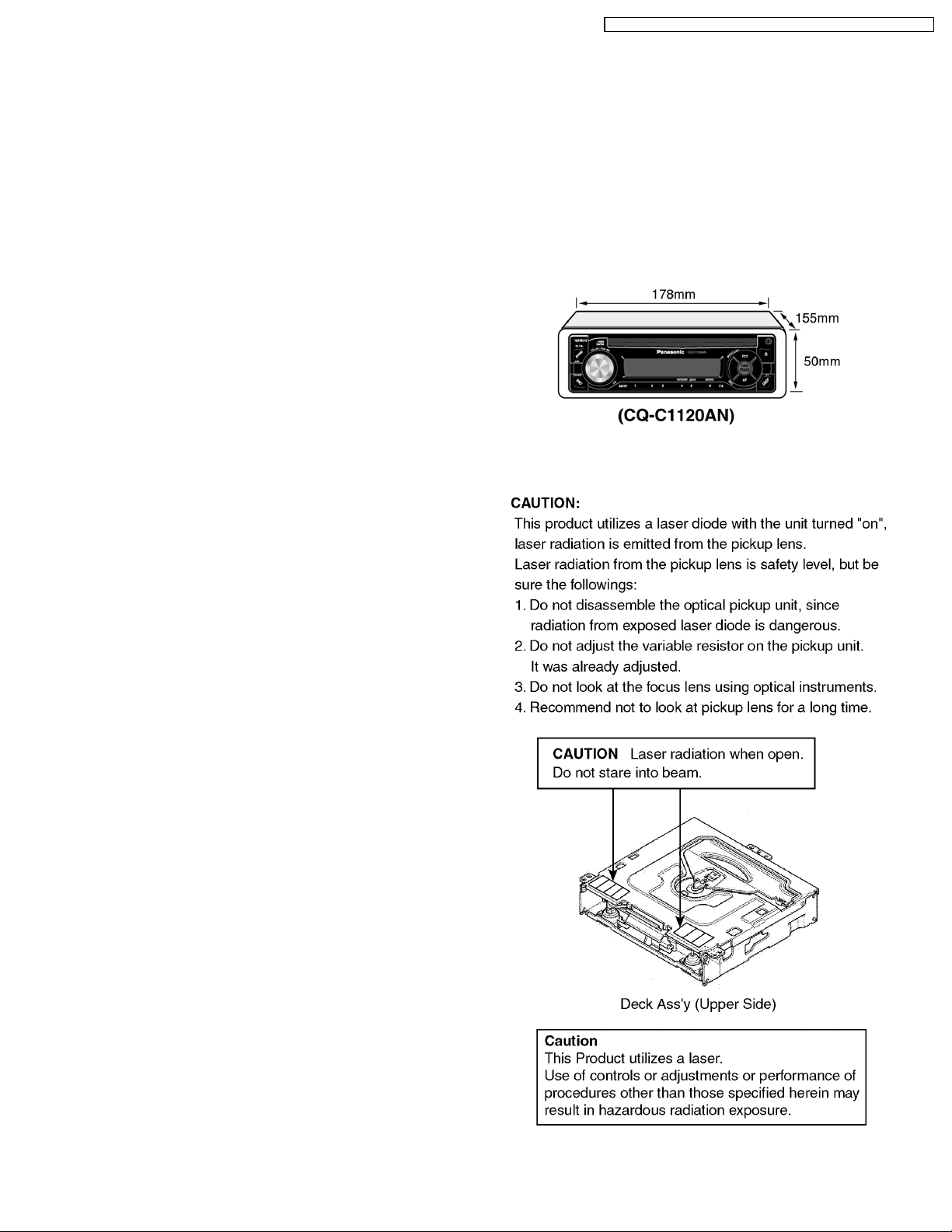
Dimensions (W×H×D)** 178×50×155mm
Weight** 1.4 kg
* Specifications and the design are subject to possible modification
without notice due to improvements.
** Dimensions and Weight shown are approximate.
** Above specifications comply with EIA standards.
© 2004 Matsushita Electric Industrial Co., Ltd. All
rights reserved. Unauthorized copying and
distribution is a violation of law.
CQ-C1120AN / CQ-C1120GN / CQ-C1110AN / CQ-C1110GN / CQ-C1100VN
CONTENTS
Page Page
1 ABOUT LEAD FREE SOLDER (PbF) 3
2 FEATURES
3 FUSE
4 MAINTENANCE
5 NOTES
6 DIMENSIONS
7 LASER PRODUCTS
8 WIRING CONNECTION
9 BLOCK DIAGRAM
10 TERMINALS DESCRIPTION
11 PACKAGE AND IC BLOCK DIAGRAM
3
3
12 REPLACEM ENT PARTS LIST
13 EXPLODED VIEW (Unit)
3
3
14 C D PLAYER MECHANISM PART
3
15 EXPLODED VIEW (CD Deck)
16 WIRING DIAGRAM
3
4
17 SCHEMATIC DIAGRAM-1
18 SCHEMATIC DIAGRAM-2
5
7
9
12
18
19
20
21
25
27
2
CQ-C1120AN / CQ-C1120GN / CQ-C1110AN / CQ-C1110GN / CQ-C1100VN
1 ABOUT LEAD FREE
SOLDER (PbF)
Distinction of PbF PCB:
PCBs (manufactured) using lead free solder will have a PbF
stamp on the PCB.
Caution :
•
• Pb free solder has a higher melting point than standard
• •
solder; Typically the melting point is 50 - 70°F (30 40°C) higher. Please use a soldering iron with
temperature control and adjust it to 700 ± 20°F (370 ±
10°C). In case of using high temperature soldering iron,
please be careful not to heat too long.
•
• Pb free solder will tend to splash when heated too high
• •
(about 1100°F/600°C)
•
• This lead free solder will be used for the products after
• •
serial No. 1,000,001.
2 FEATURES
•
• Sound System with Spurting Realism
• •
(2-channel or 4-channel Power Amplifier)
•
• Powerful Heavy Bass
• •
(Stereo/Mono Power Amplifier) : CY-M7052EN/CYM9054EN
•
• Radio Data System (RDS)
• •
•
• Not support 8 cm discs
• •
•
• Not compatible with MP3/WMA
• •
5 NOTES
[RADIO BLOCK]
Do not align the AM/FM package block. When the package
block is necessary, it will be supplied already aligned at the
factory.
[CD DECK BLOCK]
This model has no servo alignment points because
microcomputer controls the servo circuit
6 DIMENSIONS
7 LASER PRODUCTS
3 FUSE
•
• Use fuses of the same specified rating (15A).
• •
•
• Using different substitutes or fuses with higher rating, or
• •
connecting the unit directly without a fuse, could cause fire
or damage to the unit.
4 MAINTENANCE
•
• Wipe the unit with a soft dry cloth.
• •
•
• Never apply volatile liquids such as benzine and thinner to
• •
prevent damage.
3
CQ-C1120AN / CQ-C1120GN / CQ-C1110AN / CQ-C1110GN / CQ-C1100VN
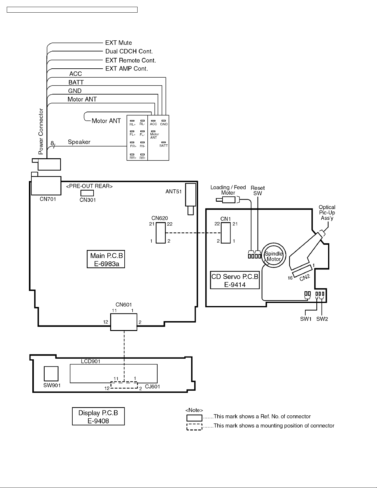
8 WIRING CONNECTION
4
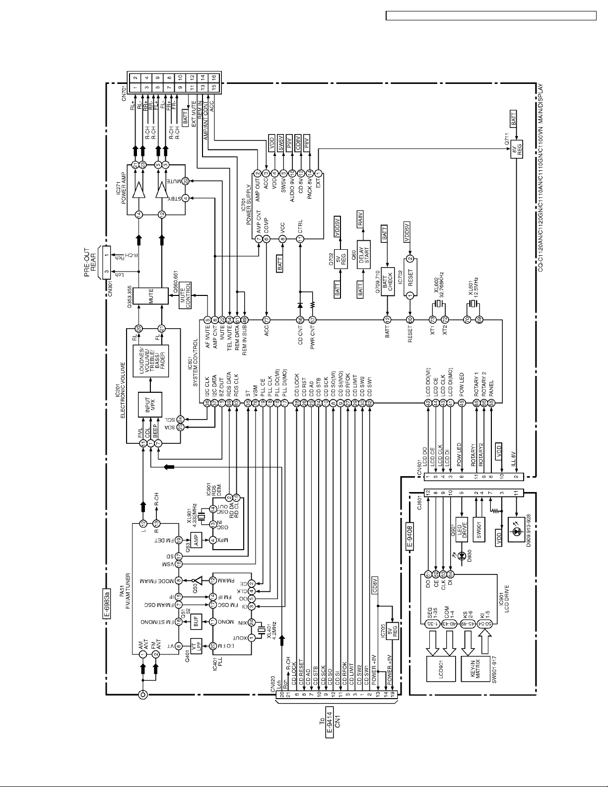
9 BLOCK DIAGRAM
9.1. Main/Display Block
CQ-C1120AN / CQ-C1120GN / CQ-C1110AN / CQ-C1110GN / CQ-C1100VN
5
CQ-C1120AN / CQ-C1120GN / CQ-C1110AN / CQ-C1110GN / CQ-C1100VN
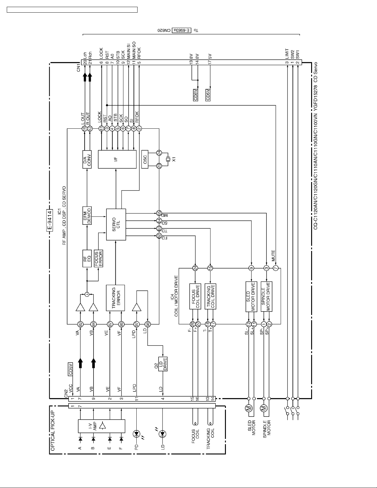
9.2. CD Servo Block
6
10 TERMINALS DESCRIPTION
CQ-C1120AN / CQ-C1120GN / CQ-C1110AN / CQ-C1110GN / CQ-C1100VN
10.1. Main Block
Pin
No.
1 NC (Ground pull down) I 0 0 0
2 NC (Ground pull down) I 0 0 0
3 NC (Ground pull down) I 0 0 0
4 AVSS Ground - 0 0 0
5 AF_MUTE AF mute O/I 5 5 5.1
6 AMP_CNT Amp control O 5 5 5.1
7 AVREF1 (Conecting to +5V) - 5 5 5.1
8 CD_S0 CD data I 0 0 0
9 CD_SI CD data O 0 0 2.8
10 CD_SCK CD clock O 0 0 5
11 CDC_DATA(NC) No connection - - - 12 BATT BATT detection I 5 5 5
13 CDC_CLK(NC) No connection - - - 14 REW_OUT(NC) No connection - - - 15 BZ_OUT Buzzer signal output O 0 0 0
16 PLL_D0 PLL data I 5.1 5.1 5.1
17 PLL_DI PLL data O 0 0 0
18 PLL_CLK PLL clock O 5 5 5.1
19 PLL_CE PLL chip enable O 0 0 0
20 NC No connection - - - 21 NC No connection - - - 22 MUTE Mute control output O 5 5 5.1
23 NC No connection - - - 24 CD_STB CD strobe - 0 0 5
25 CD_AO CD AO - 0 0 4.4
26 CD_RST(NC) No connection - - - 27 CD_RFOK CD RFOK I 0 0 4.9
28 CD_LOCK CD lock I 0.5 0.3 4.9
29 CD_LIMIT CD limit I 0 0 5
30 CD_SW2 CD SW2 I 5 5 0
31 NC No connection - - - 32 NC No connection - - - 33 VSS1 Ground - 0 0 0
34 NC No connection - - - 35 ST FM stereo signal input I 5 5.1 5
36 SCL Audio control clock O 5 5 5.1
37 SDA Audio control data I/O 5 5 5.1
38 S_LED(NC) No connection - - - 39 NC No connection - - - 40 NC No connection - - - 41 LCD_DI LCD driver data O 0 0 0
42 LCD_DO LCD driver data I 5 5 5
43 LCD_CLK LCD driver clock O 0 0 0
44 LCD_CE LCD driver chip enable O 0 0 0
45 POW_LED Power LED O/I 0 0 0
46 ANT_CNT(NC) No connection - - - 47 ILL_CNT(NC) No connection - - - 48 NC No connection - - - 49 REM.IN_SUB Remote control sub data I 5 5 5
50 NC No connection - - - 51 NC No connection - - - 52 NC No connection - - - 53 NC No connection - - - 54 TEL MUTE TEL mute I 5 5 5
55 PANEL PANEL in detection I 4.8 4.8 4.8
56 CD_CNT CD power control O 0 0 5
57 PWR_CNT Main power control O 5 5 5.1
58 NC No connection - - - 59 RDS_DATA RDS data input I 2.8 0 2.8
60 RESET System reset I 5 5 5.1
61 REM_DATA Remote control data I 5 5 5
Port Description I/O (V)
IC601 : C2CBHF000322
FM AM CD
Pin
No.
62 CD_SW1 CD SW1 signal input I 0 0 0
63 RDS_CLK RDS clock input I 2.6 2.5 2.6
64 CDC_STB Changer strobe signal I 0 0 0
65 ROT.1 Rotary encoder signal 1 I 5 5 5.1
66 ROT.2 Rotary encoder signal 2 I 5 5 5.1
67 VSS0 Ground - 0 0 0
68 VDD1 +5V power supply - 5 5 5.1
69 X2 Crystal oscillator - 2.8 2.8 2.8
70 X1 Crystal oscillator I 2.6 2.6 2.6
71 VPP Vpp - 0 0 0
72 XT2 SUB Crystal oscillator - 2.8 2.8 2.8
73 XT1 SUB Crystal oscillator I 2.5 2.5 2.5
74 VDD0 +5V power supply - 5 5 5.1
75 AVREF +5V power supply - 5 5 5.1
76 VSM FM/AM SD input I 0.5 0.8 0
77 ACC ACC detection I 5.2 5.2 5.2
78 INIT_A (+5V pull up) I 5 5 5.1
79 NC (Ground pull down) I 0 0 0
80 NC (Ground pull down) I 0 0 0
Port Description I/O (V)
FM AM CD
10.2. Display Block
Pin No. Port Description I/O (V)
1-35 S1-35 LCD segment data O 2.5
36-39 NC No connection - 40-43 COM1-4 LCD common O 2.5
44 KS1 Not used - 45-49 KS2-6 Key scan O 5
50-54 Kl1-5 Key data I 0
55 TEST (Connecting to ground) - 0
56 VDD +5V power supply - 5
57 VDD1 VDD1 filter terminal - 3.3
58 VDD2 VDD2 filter terminal - 1.7
59 VSS Ground - 0
60 OSC Oscillator terminal - 3.9
61 DO Key data output O 5
62 CE LCD driver chip enable I 0
63 CLK LCD clock I 4.9
64 DI LCD data I 4.9
IC901 : YEAMLC75854T
7
CQ-C1120AN / CQ-C1120GN / CQ-C1110AN / CQ-C1110GN / CQ-C1100VN
10.3. CD Servo Block
Pin
No.
10 D.VDD Digital Power Supply - 4.9
11 DA.VDD D/A Converter Power Supply - 4.7
12 ROUT R-channel Audio Signal Output O 3.3
13 DA.GND D/A Converter Ground - 0
14 REGC Capacitor Connection for Regulator - 3.4
15 DA.GND D/A Converter Ground - 0
16 LOUT L-channel Audio Signal Output O 3.3
17 DA.VDD D/A Converter Power Supply - 4.6
18 R+(NC) No connection - 19 R-(NC) No connection - 20 L-(NC) No connection - 21 L+(NC) No connection - 22 X.VDD Crystal Oscillator Power Supply - 4.8
23 XTAL Crystal Connection O 2.3
24 /XTAL Crystal Connection I 2.1
25 X.GND Crystal Oscillator Ground - 0
26 D.VDD Digital Power Supply - 4.7
27 EMPH(NC) No connection - 28 FLAG(NC) No connection - 29 DIN Data Input I 2.5
30 DOUT Data Output O 2.5
31 SCKIN Serial Clock Input I 2.7
32 SCKO Serial Clock Output O 2.7
33 LRCKIN LR Clock Input I 2.5
34 LRCK LR Clock O 2.5
35 HOLD/WDC
36 TX(NC) No connection - 37 D.GND Digital Ground - 0
38 C16M(NC) No connection - 39 LIMIT(NC) No connection - 40 D.VDD Digital Power Supply - 4.9
41 LOCK Lock O 4.9
42 RFCK(NC) No connection - 43 MIRR/WFC
44 PLCK(NC) No connection - 45 D.GND Digital Ground - 0
46 C1D1(NC) No connection - 47 C1D2(NC) No connection - 48 C2D1(NC) No connection - 49 C2D2(NC) No connection - 50 C2D3(NC) No connection - 51 D.VDD Digital Power Supply - 4.9
52 PACK(NC) No connection - 53 TSO(NC) No connection - 54 TSI Parameter Input for Text Data I 0
55 /TSCK Serial Clock for Text Data I 0
56 TSTB Text Parameter Strobe I 0
57 D.GND Digital Ground - 0
58 TEST0 Test I 0
59 TEST1 Test I 0
60 ATEST Analog Test O 2.0
61 A.GND Analog Ground - 0
62 FD Focus Drive O 2.5
Port Description I/O (V)
1 D.GND Digital Ground - 0
2 RFOK RFOK Signal O 4.9
3 /RESET Reset I 4.9
4 A0 Address 0 I 4.0
5 /STB Strobe I 4.9
6 /SCK Serial Clock I 4.9
7 SO Serial Data Output O 0
8 SI Serial Data Input I 3.0
9 /XTALEN Crystal Oscillaton Enable I 0
K(NC)
K(NC)
IC1 : C1BB00000665
No connection - -
No connection - -
Pin
No.
63 TD Tracking Drive O 2.5
64 SD Sled Drive O 2.6
65 MD Motor Drive O 2.5
66 DAC0(NC) No connection - 67 DAC1(NC) No connection - 68 DAC2(NC) No connection - 69 DAC3(NC) No connection - 70 A.VDD Digital Power Supply - 4.9
71 EFM EFM Signal O 2.7
72 ASY Slice Level I 2.4
73 C3T Capacitance Connection for 3T Signal
74 RFI RF Signal Input I 2.4
75 AGCO AGC Amp Output O 2.4
76 AGCI AGC Amp Input I 2.4
77 RFO RF Amp Output O 2.7
78 EQ2 Equalizer Parts Connection for RF
79 EQ1 Equalizer Parts Connection for RF
80 RF- Impedance Connection to RF Amp for
81 A.GND Analog Ground - 0
82 A Error Signal Input I 2.7
83 C(NC) No connection - 84 B Error Signal Input I 2.7
85 D(NC) No connection - 86 F Error Signal Input I 2.9
87 E Error Signal Input I 2.9
88 A.VDD Analog Power Supply - 4.9
89 REFOUT Reference Output O 2.5
90 FE- Impedance Connection to Focus Error
91 FEO Focus Error Amp Output O 2.5
92 TE- Impedance Connection to Ttacking
93 TEO Tracking Error Amp Output O 2.5
94 TE2 Tracking Error Amp Output Multiplied
95 TEC Tracking Error Comparator I 2.5
96 A.GND Analog Ground - 0
97 PD Photo Diode Signal (for Detecting
98 LD Laser Diode Control Current Output O 3.6
99 PN APC Circuit Polarity Control I 0
100 A.VDD Analog Power Supply - 4.9
Port Description I/O (V)
- 2.7
Detecting Circuit
- 2.5
Amp
- 0.3
Amp
I 2.3
Negative Feedback
I 2.5
Amp for Negative Feedback
I 2.5
Error Amp for Negative Feedback
O 2.6
by Two
I 0.2
Laser Power) Input
8
CQ-C1120AN / CQ-C1120GN / CQ-C1110AN / CQ-C1110GN / CQ-C1100VN
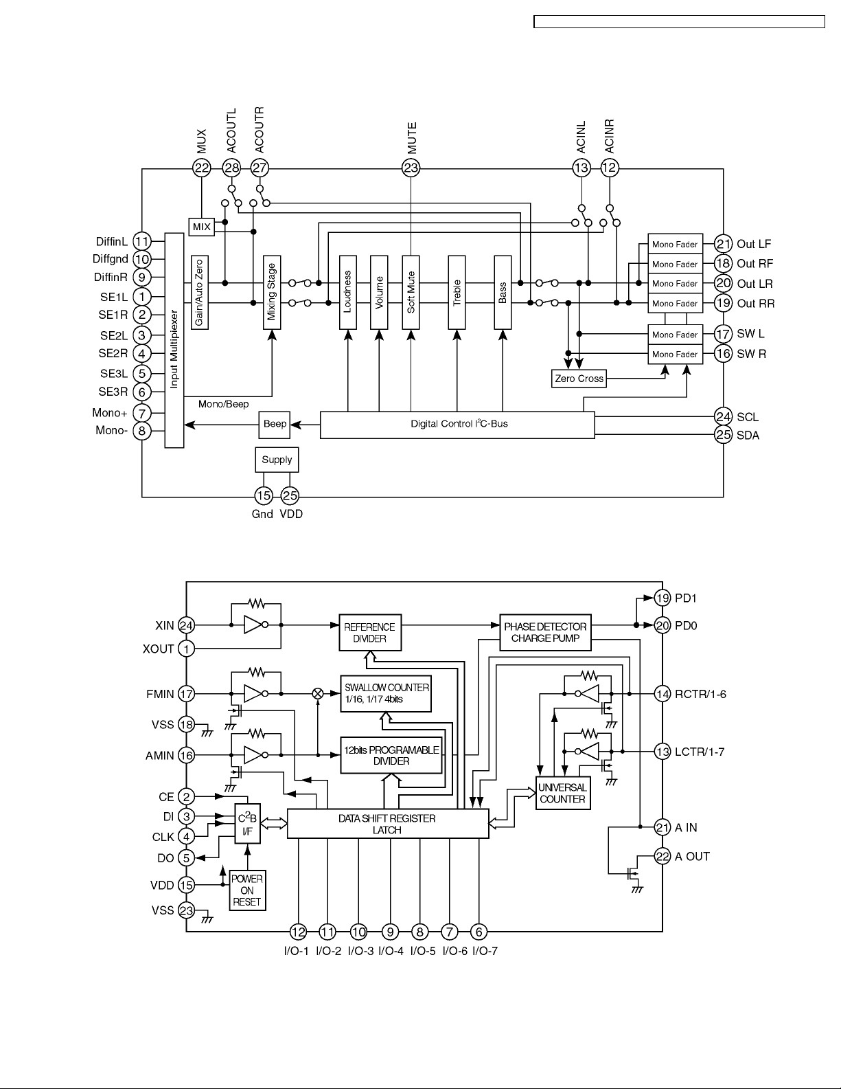
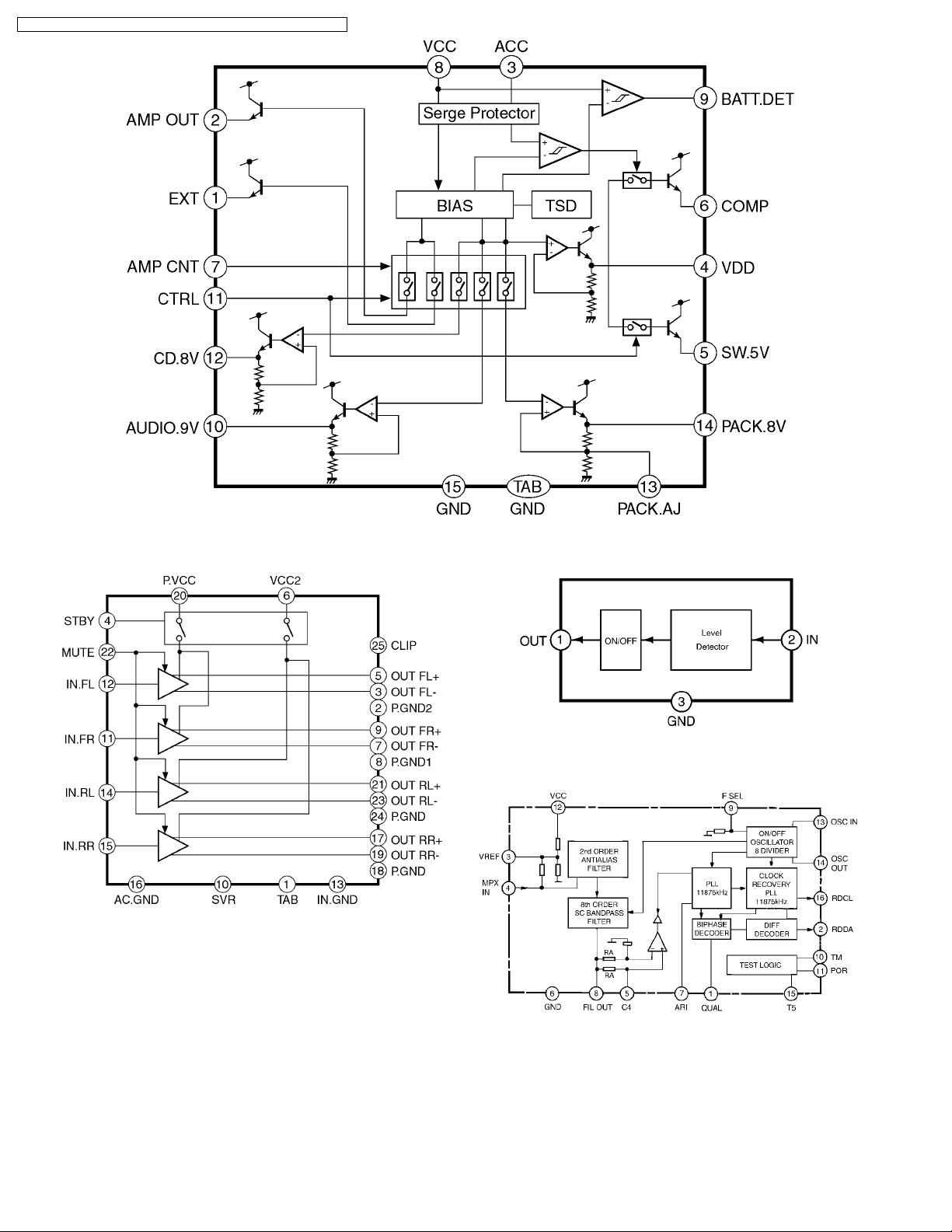
11 PACKAGE AND IC BLOCK DIAGRAM
11.1. Main Block
IC201 : C1BB00000543
IC401 : C1BB00000644
9
CQ-C1120AN / CQ-C1120GN / CQ-C1110AN / CQ-C1110GN / CQ-C1100VN
IC271 : C1EA00000036
IC701 : C0DAZHH00007
IC702 : MN1382QTX
10
IC901 : YEAMDA7479D
 Loading...