

Page 1
Specifications*
Order No. ACED051204C7
C4
AUTOMOTIVE AFTERMARKET
CQ-C1103U
Removable Front Panel CD Player /
Receiver
General
Power Supply DC 12V (11V - 16V),
Test Voltage 14.4V
Negative Ground
Tone Controls Bass ; ±12dB at 100Hz
Treble ; ±12dB at 10kHz
Current Consumption Less than 2.2A (CD play mode,
0.5W×4ch)
Maximum Power Output 50W×4ch (at 1kHz, Vol. Max.)
Suitable Speaker Impedance 4-8Ω
Pre-Amp Output Voltage 2.5V (CD play mode; 1kHz, 0dB)
Output Impedance 200Ω
FM Stereo Radio
Frequency Range 87.9 - 107.9MHz
Usable Sensitivity 11.0dBf (1.25µV, 75Ω)
AM Radio
Frequency Range 530 - 1,710kHz
Usable Sensitivity 28dB/µV (25µV, S/N 20dB)
CD Player
Sampling Frequency 8 times oversampling
Pick-Up Type Astigma 3-beam
Light Source Semiconductor Laser
Wavelength 780nm
Frequency Response 20Hz to 20,000Hz (±1dB)
Signal to Noise Ratio 96dB
Dimensions** 178×50×155mm
Weight** 1.4kg
* Specifications and the design are subject to possible modification
without notice due to improvements.
** Dimensions and Weight shown are approximate.
© 2005 Matsushita Electric Industrial Co., Ltd. All
rights reserved. Unauthorized copying and
distribution is a violation of law.
Page 2
CQ-C1103U
CONTENTS
Page Page
1 ABOUT LEAD FREE SOLDER (PbF) 2
2 FEATUERS
3 LASER PRODUCTS
4 REPLACEING THE FUSE
5 MAINTENANCE
6 NOTES
7 DIMENSIONS
8 WIRING CONNECTION
9 BLOCK DIAGRAM
10 TERMINALS DESCRIPT ION
11 PACKAGE AND IC BLOCK DIAGRAM 8
2
12 REPLACEMENT PARTS LIST
2
13 EXPLODE D VIEW (Unit)
14 CD PLAYER MECHANICAL PARTS LIST
2
3
15 EXPLODE D VIEW (CD Deck)
3
16 PACKING PARTS LIST
17 WIRING DIAGRAM
3
4
18 SCHEMATIC DIAGRAM-1
5
19 SCHEMATIC DIAGRAM-2
20 SCHEMATIC DIAGRAM for printing with A4 size
6
12
17
18
19
20
21
25
27
29
1 ABOUT LEAD FREE
SOLDER (PbF)
Distinction of PbF PCB:
PCBs (manufactured) using lead free solder will have a PbF
stamp on the PCB.
Caution :
•
• Pb free solder has a higher melting point than standard
• •
solder; Typically the melting point is 50 - 70°F (30 40°C) higher. Please use a soldering iron with
temperature control and adjust it to 700 ± 20°F (370 ±
10°C). In case of using high temperature soldering iron,
please be careful not to heat too long.
•
• Pb free solder will tend to splash when heated too high
• •
(about 1100°F/600°C)
•
• This lead free solder will be used for the products after
• •
serial No. 1,000,001.
2 FEATUERS
•
• 18-FM, 6-AM presets with preset scan
• •
•
• Digital servo for reliable CD playback.
• •
•
• Removable face plate.
• •
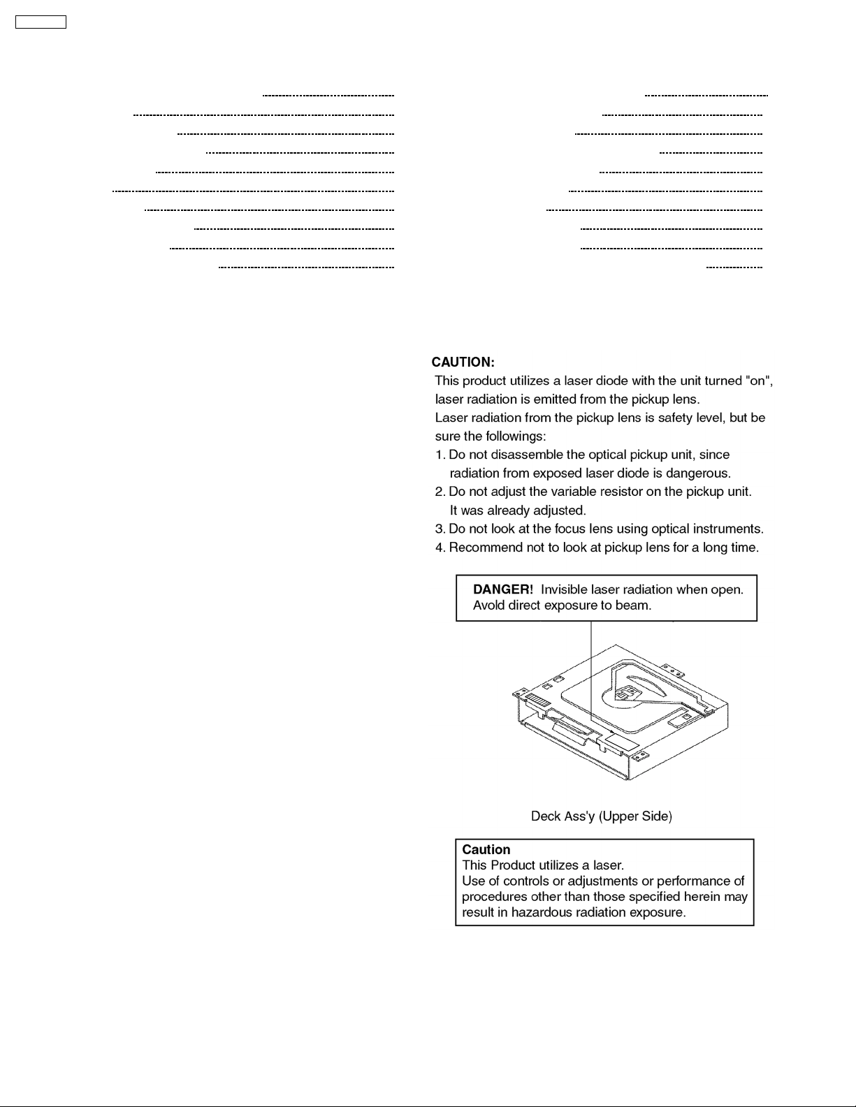
3 LASER PRODUCTS
4 REPLACEING THE FUSE
Use fuses of the same specified rating (15A). Using different
substitutes or fuses with higher ratings, or connecting the
product directly without a fuse, could cause fire or damage to
the stereo unit.
2
Page 3
5 MAINTENANCE
Your products is designed and manufactured to ensure a
minimum of maintenance. Use a dry, a soft cloth for routine
exterior cleaning. Never use benzine, thinner or other solvents.
6 NOTES
[RADIO BLOCK]
Do not align the AM/FM package block. When the package
block is necessary, it will be supplied already aligned at the
factory.
[CD DECK BLOCK]
This model has no servo alignment points because
microcomputer controls the servo circuit.
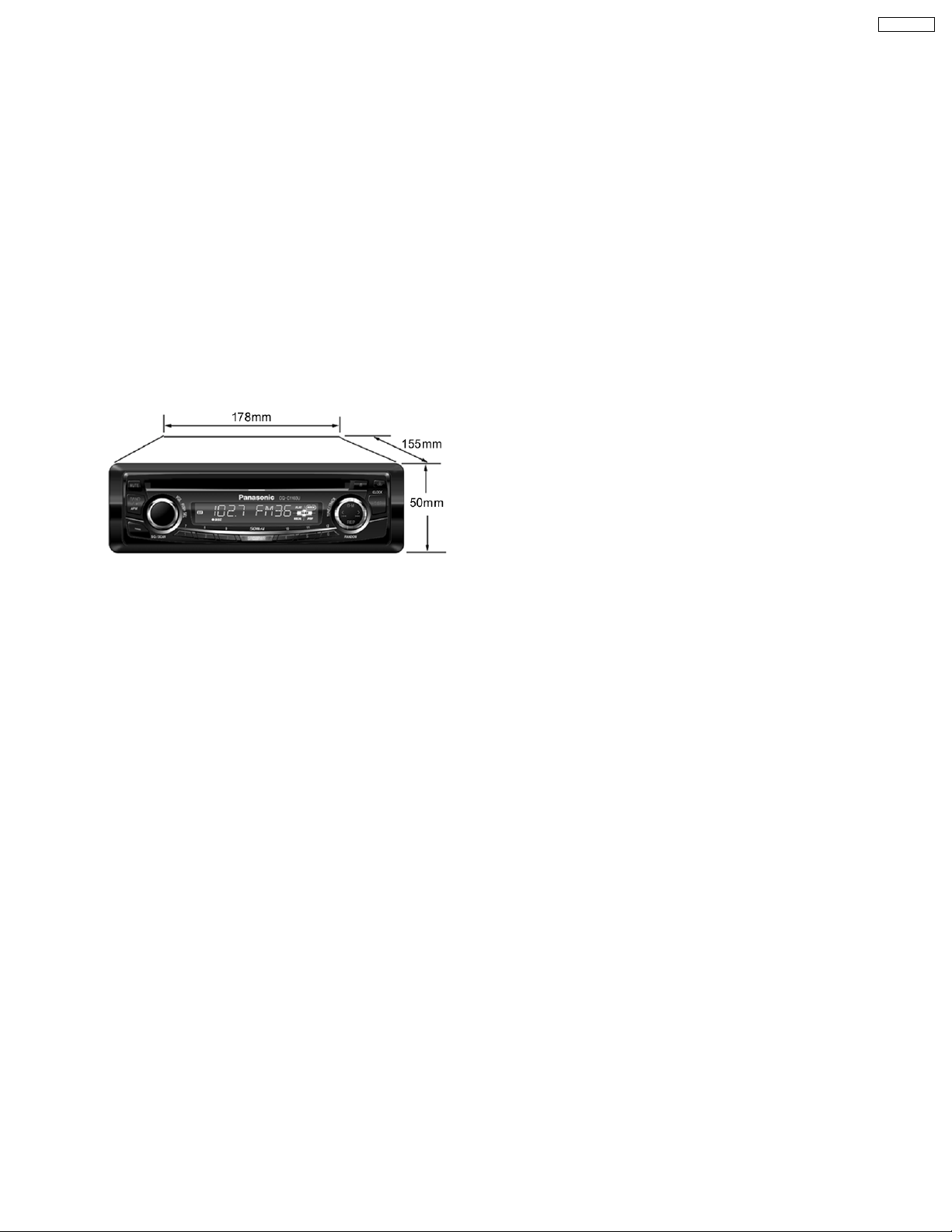
7 DIMENSIONS
CQ-C1103U
3
Page 4
CQ-C1103U
8 WIRING CONNECTION
4
Page 5
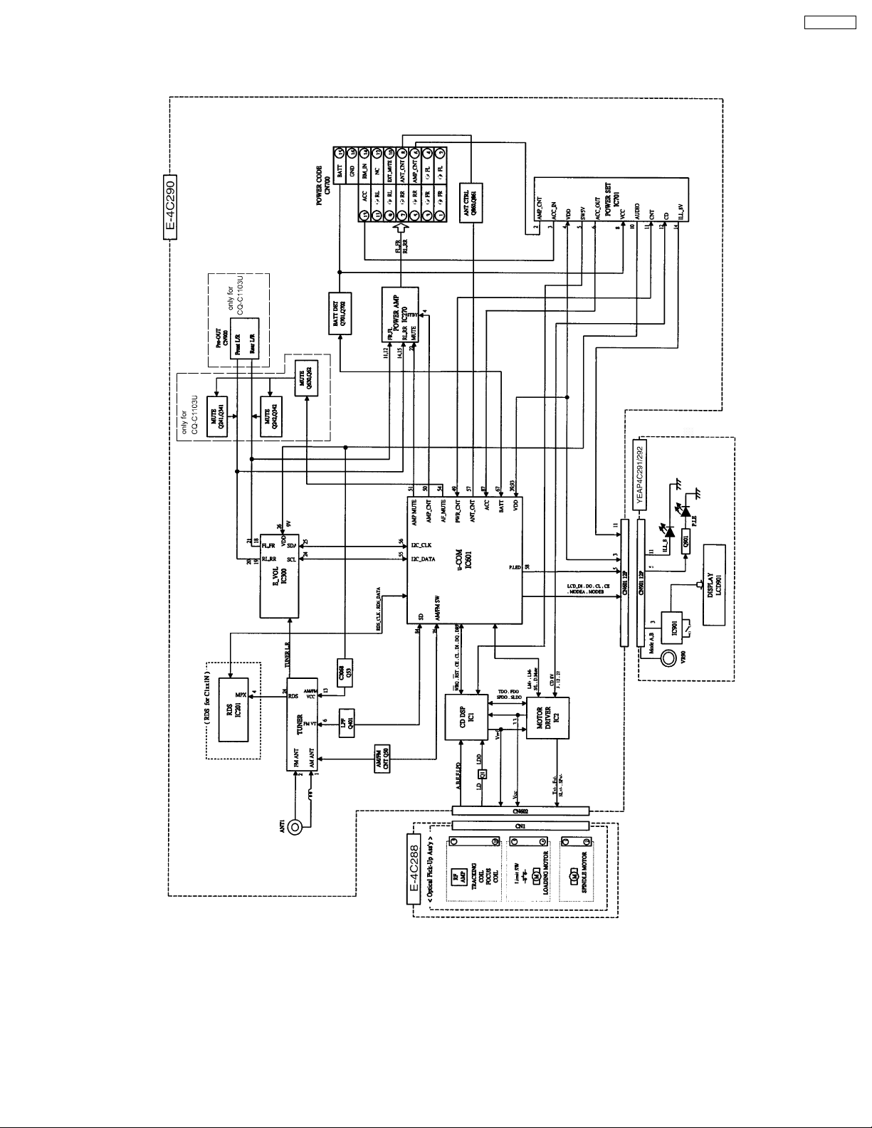
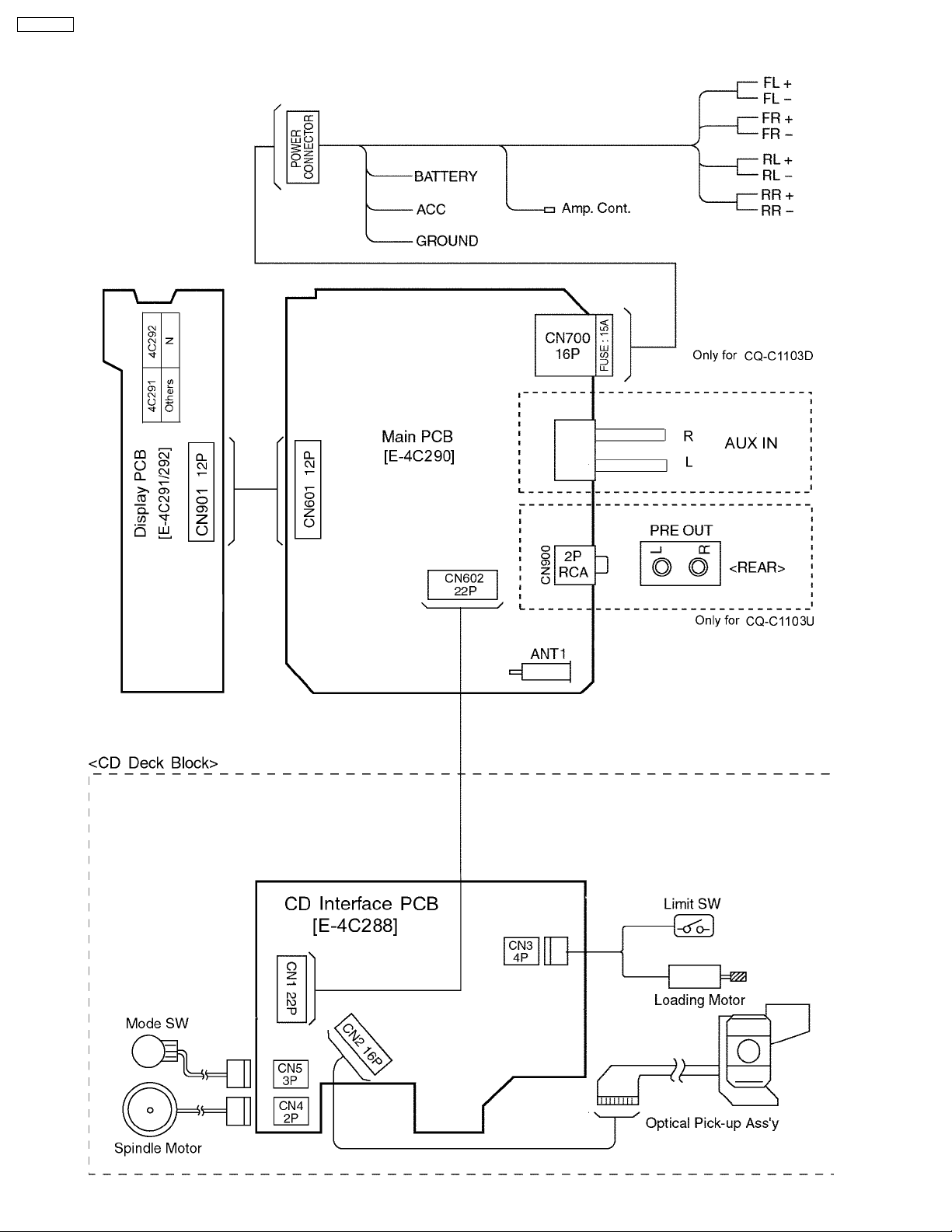
9 BLOCK DIAGRAM
CQ-C1103U
5
Page 6
CQ-C1103U
10 TERMINALS DESCRIPTION
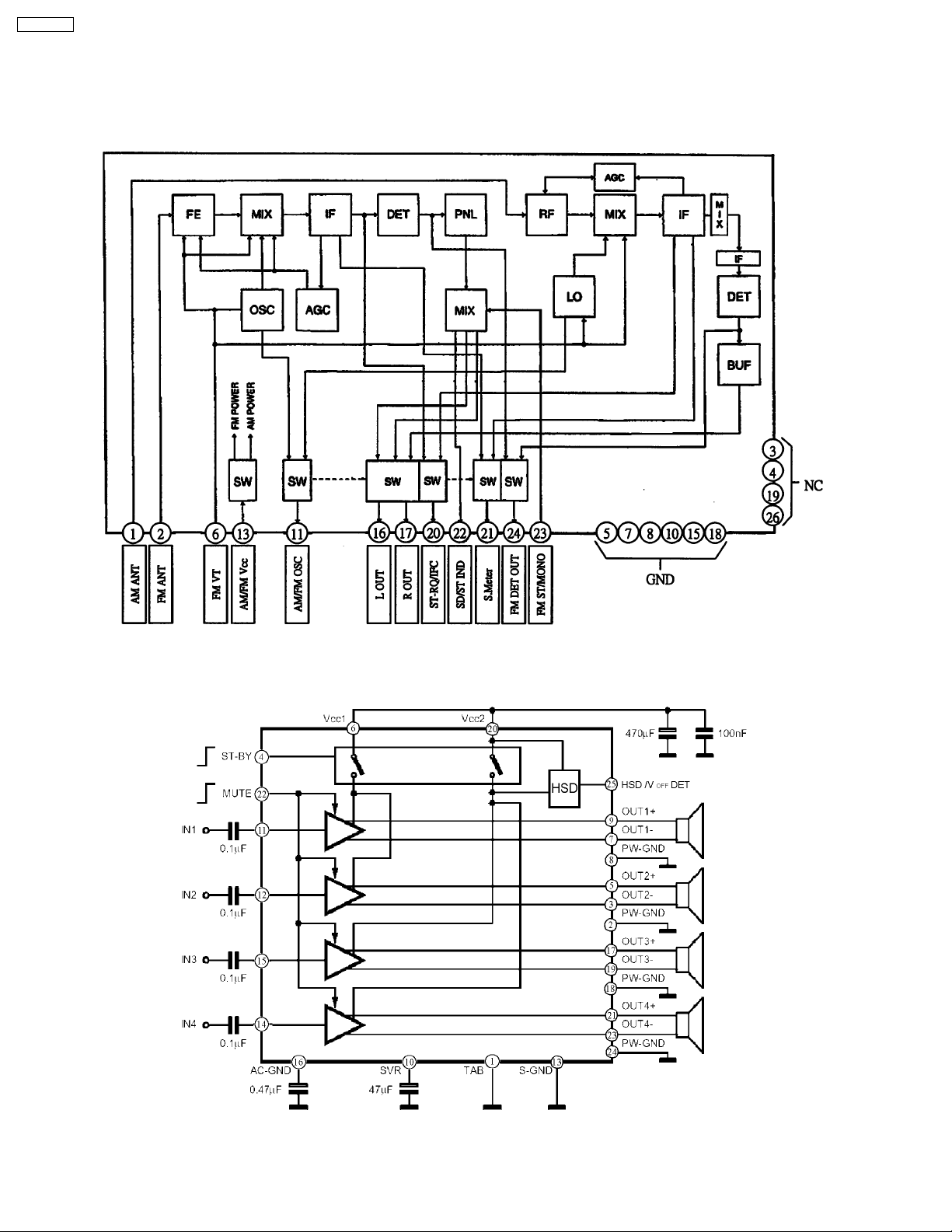
10.1. Main Block
IC601 : LC7237819D07
Ref.
Part
No.
1 XIN 4. 5 MHz X’tal and
2 TEST2 GND connection I 0 0 0
3 VREG Bypass condenser
4 VSSCPU GND connection - 0 0 0
5 CDC_DATACD changer data I 0 0 0
6 N.C. None - - - 7 CDC_CLK CD changer clock I 0 0 0
8 CDC_REM
_OUT
9 LCD_DO LCD data output I 5,22 5,22 5.18
10 LCD_DI LCD data input O 0 0 0
11 LCD_CLK LCD clock O 5.17 5.19 5.15
12 LCD_CE LCD chip enable output O 0.1 0.14 0.12
13 CD_DO CD data output I 5.34 5.35 5.12
14 CD_DI CD data input O 0 0 5.2
15 CD_CLK CD clock O 5.19 5.21 5.17
16 CD_CE CD chip enable O 0 0 0.25
17 CD_LM+ CD eject O 0 0 0
18 CD_LM- CD loading O 0 0 0
19 CD_S/L CD 24PIN connection O 0 0 5.21
20 CD_WRQ CD WRQ connection I 5.34 5.35 4.26
21 CD_INSW1CD insert SW input I 0.1 0 0.1
22 CD_SW2 CD MECHA SW2 I 5.17 5.21 0.1
23 CD_LIMI
T_SW
24 CD_DRF CD DRF I 0 0 5.33
25 CD_RST CD reset O 5.19 5.22 5.21
26 CD_MUTE CD mute O 0 0 5.2
27 N.C. None - - - 28 N.C. None - - - 29 PANEL Panel detect I 5.2 5.23 5.2
30 N.C. GND connection I 0 0 0
31 N.C. GND connection I 0 0 0
32 N.C. GND connection I 0 0 0
33 N.C. None - - - 34 N.C. None - - - 35 N.C. None - - - 36 N.C. None - - - 37 N.C. None - - - 38 N.C. None - - - 39 VDDPORT Power supply of PORT - 5.19 5.22 5.21
40 VSSPORT GND of PORT - 0 0 0
41 N.C. None - - - 42 N.C. None - - - 43 N.C. None - - - 44 N.C. None - - - 45 N.C. None - - - 46 N.C. None - - - 47 N.C. None - - - 48 N.C. None - - - 49 PWR_CNT Power control O 5.12 5.2 5.19
50 AMP_CNT Amp stand-by O 5.12 5.2 5.19
51 AMP_MUTEAmp mute O 5.19 5.21 5.21
52 N.C. None - - - 53 SSC Tuner search sensitivity
54 AF_MUTE AF mute O 5.19 5.21 5.21
55 I2C_DATAElectronic VOL data O 5.2 5.21 5.21
56 I2C_CLK Electronic VOL clock O 5.2 5.21 5.21
57 ANT_CNT Motor antena control O 5.19 5.21 0
58 POWER_LEDPower LED O 0.15 0.15 0.12
59 N.C. None - - - -
Part Name & Description I/O(V) FM(V)AM(V)CD(V
No.
Connection
connected.
CD changer Remote out O 0 0 0
CD limit SW I 0 0 5.18
change
I 2.52 2.53 2.52
O 2.9 2.9 2.93
O 0 0 0
Ref.
Part
No.
)
60 N.C. (
BZ_OUT
)
61 N.C. None - - - 62 N.C. None - - - 63 N.C. None - - - 64 N.C. None - - - 65 N.C. None - - - 66 TEL_MUTEExternal MUTE input I 5.36 5.35 5.33
67 BATT Battery detection I 5.36 5.35 5.33
68 MODE_B ROTARY B input I 5.17 5.18 0
69 N.C.(RD
S_CLK)
70 REM_IN Remocon data input I 0 0 0
71 MODE_A ROTARY A input I 5.17 5.13 5.16
72 CDC_STB CD changer strobe input I 0 0 0
73 NC None - - - 74 MONO Compulsion MONO ON O 0 0 0
75 AM_MODE AM change O 8.21 0.13 8.23
76 FM_MODE FM change O 0.13 8.2 8.23
77 N.C. GND connection I 0 0 0
78 INIT_C Initial value C I 0 0 0
79 INIT_B Initial value B I 5.16 5.19 5.19
80 INIT_A Initial value A I 0 0 0
81 VSS GND connection - 0 0 0
82 N.C.(RD
S_DATA)
83 ST FM stereo input I 5.34 5.2 5.4
84 SD_FM/AMSignal detection I 3.12 3.43 0
85 N.C. GND connection I 0 0 0
86 RESET Reset Input I 5.2(
87 ACC Power supply I 5.42 5.42 5.42
88 N.C. GND connection I 0 0 0
89 N.C. GND connection I 0 0 0
90 FM/AM_IFCFM/AM IF input I 1.42 1.42 0
91 N.C. GND connection I 0 0 0
92 SUBPD None O 2 2.02 0
93 VDDPLL Power supply of PLL - 5.23 5.22 5.2
94 N.C. GND connection I 0 0 0
95 OSC_FM/AMFM/AM osc input I 1.39 1.26 0
96 VSSPLL GND connection - 0 0 0
97 N.C. None - - - 98 EO1 PLL phase comparison
99 TEST1 GND connection I 0 0 0
100 XOUT 4. 5 MHz X’tal and
Part Name & Description I/O(V) FM(V)AM(V)CD(V
No.
None - - - -
None - - - -
None - - - -
error output
Connection
Note 1 :
Voltage measuerments are with respect to ground, with a
voltmeter (internal resistance : 10M ohms).
10.2. Display Block
IC901 : YEAMLC75853NW
Pin No. Port Descriptions I/O
1-4 NC No connection - -
5-31 SEG5-31 LCD segment O 2.5
32-40 NC No connection - 41-43 COM1-3 LCD common O 2.5
44-49 KS1-6 Key data output O 0.9
)
6.4(
PWR
OFF)
(V)
5.2(
EJEC
T)
(V)
PWR
OFF)
O 2 2.02 0
O 2.62 2.63 2.62
6
Page 7

Pin No. Port Descriptions I/O
50-54 KI1-5 Key data input I 0
55 TEST (Connecting to ground) - 0
56 VDD +5V power supply - 5.1
57 VDD1 Ground through capacitor - 3.3
58 VDD2 Ground through capacitor - 1.7
59 Vss Ground - 0
60 OSC CR oscillator - 3.9
61 DO Key data output O 4.4
62 CE Chip enable I 0
63 CLK LCD clock I 0
64 DI LCD data input I 0
(V)
CQ-C1103U
(V)
7
Page 8
CQ-C1103U
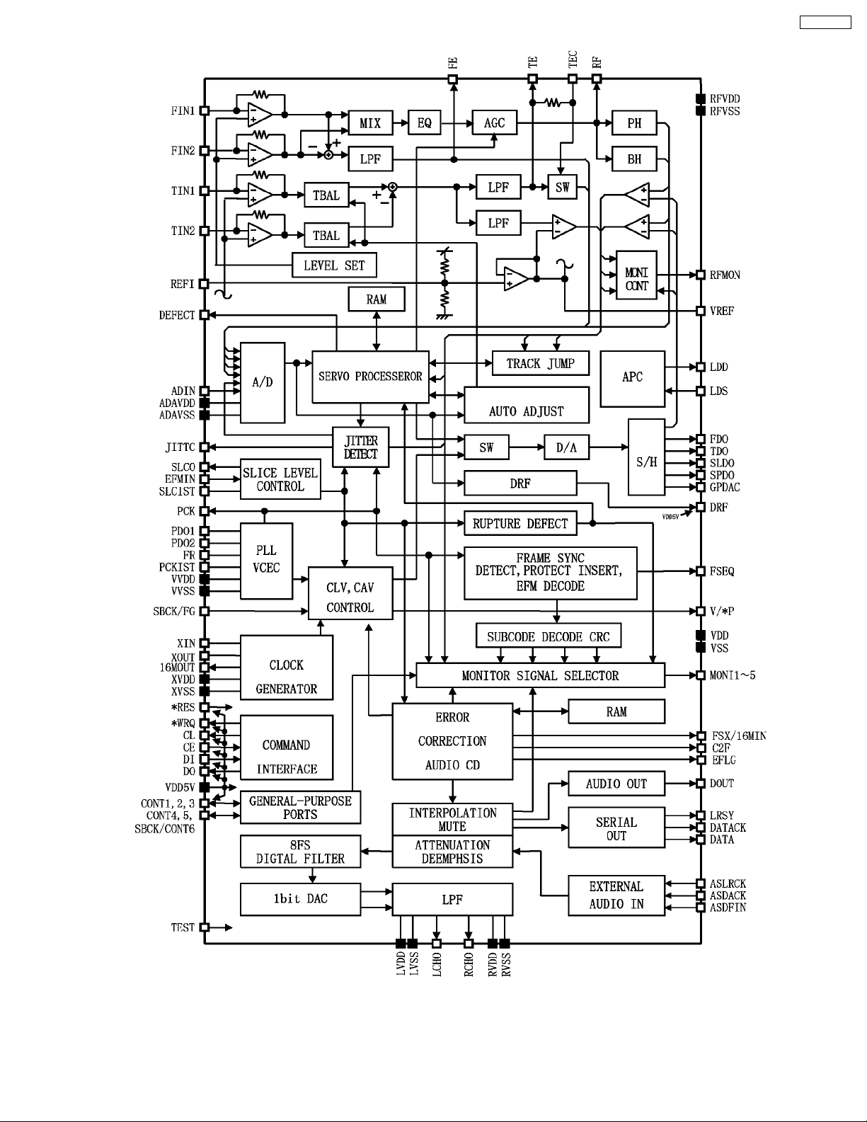
11 PACKAGE AND IC BLOCK DIAGRAM
11.1. Main Block
P50:J3CCBB000005
IC270 : C1EA00000041
8
Page 9
CQ-C1103U
IC1 : C1BB00001089
9
Page 10

CQ-C1103U
IC300 : C1BB00000543
IC2 : C1BB00001088
10
Page 11

CQ-C1103U
IC701 : C0DAZHF00004
11
Page 12

CQ-C1103U
12 REPLACEMENT PARTS LIST
Ref.
No.
1. IC’s and Transistors
MAIN BLOCK [E-4C290]
IC1 C1BB00001089 IC T
IC2 C1BB00001088 IC T
IC270 C1EA00000041 IC T
IC300 C1BB00000543 IC T
IC601 LC7237819D07 IC T
IC701 C0DAZHF00004 IC T
P50 J3CCBB000005 Tuner T
Q1 YEAN2SA1317T Transistor T
Q2 B1BCCF000013 Transistor T
Q241 YEANKRC110S Transistor T
Q242 YEANKRC110S Transistor T
Q341 YEANKRC110S Transistor T
Q342 YEANKRC110S Transistor T
Q401 YEAN2SK583T Transistor T
Q50 B1GDCFEH0001 Transistor T
Q53 YEAN2SC3068T Transistor T
Q54 B1GDCFEH0001 Transistor T
Q62 YEANKRA104M Transistor T
Q630 YEANKRA104M Transistor T
Q701 YEANKRA104M Transistor T
Q702 B1GACFCJ0003 Transistor T
DISPLAY BLOCK [E-4C291]
IC901 YEAMLC75853NW LCD DRIVER IC T
Q901 YEANKRA102S Transistor T
2. Diodes
MAIN BLOCK [E-4C290]
D604 B0ACCK000005 Diode T
D605 B0ACCK000005 Diode T
D610 YEAD1N4148C Diode T
D706 B0BC6R700006 Diode T
D707 YEADSM5819A Diode T
D708 YEAD1N5404FT Diode T
D710 YEAD1N4005ST Silicon Diode T
D714 YEAD1N4005ST Silicon Diode T
D961 YEAD1N4005ST Silicon Diode T
D962 YEAD1N4005ST Silicon Diode T
D963 YEAD1N4005ST Silicon Diode T
D964 YEAD1N4005ST Silicon Diode T
D965 YEAD1N4005ST Silicon Diode T
D966 YEAD1N4005ST Silicon Diode T
Part No. Part Name & Description Remarks
Ref.
No.
D967 YEAD1N4005ST Silicon Diode T
D968 YEAD1N4005ST Silicon Diode T
Z52 D4ZZ00000024 Surge Protector T
DISPLAY BLOCK [E-4C291]
D900 B3AFB0000039 LED T
D900 B3AAB0000213 CHIP LED (WHITE) T
D907 MAZ80560ML Zener Diode T
D919 YEADSPADB01 LED (BLUE) T
D920 YEADSPADR01 LED (Red) T
D921 YEADSPADR01 LED (Red) T
D922 YEADSPADR01 LED (Red) T
D923 YEADSPADR01 LED (Red) T
D924 YEADSPADR01 LED (Red) T
D925 YEADSPADR01 LED (Red) T
D926 YEADSPADR01 LED (Red) T
D927 YEADSPADR01 LED (Red) T
D928 YEADSPADR01 LED (Red) T
D929 YEADSPADR01 LED (Red) T
D930 YEADSPADR01 LED (Red) T
3. Capacitors
MAIN BLOCK [E-4C290]
C1 ECEA1AKA330IV Electrolytic 33PF 10WV T
C2 F1J1H103A733 Ceramic 0.01MFD 50WV T
C3 F1J1H104A036 Ceramic 0.1MFD 50WV T
C4 F1J1H104A036 Ceramic 0.1MFD 50WV T
C5 F1J1H102A733 Ceramic 1000pF 50WV T
C6 EEAFC0J560H Electrolytic 56PF 6.3WV T
C7 F1J1H103A733 Ceramic 0.01MFD 50WV T
C8 ECEA1AKA221IV Electrolytic 220PF 10WV T
C9 F1J1H104A036 Ceramic 0.1MFD 50WV T
C10 F2A0J101A049 Electrolytic 100pF 6.3WV T
C11 F1J1H104A036 Ceramic 0.1MFD 50WV T
C12 F1J1H101A732 Ceramic 100pF 50WV T
C13 F1J1H473A733 Ceramic 0.047MFD 50WV T
C14 F1J1H472A733 Ceramic 0.0047MFD 50WV T
C15 F2A1C100A041 Electrolytic 10pF 16WV T
C16 ECUV105K16AT Ceramic 1MFD 16WV T
C17 F1J1H470A732 Ceramic 47pF 50WV T
C18 F1J1H104A036 Ceramic 0.1MFD 50WV T
C19 F2A0J101A020 Electrolytic 100pF 6.3WV T
C20 F2A1A101A354 Electrolytic 100pF 10WV T
C21 F2A0J101A049 Electrolytic 100pF 6.3WV T
C22 F2A0J101A020 Electrolytic 100pF 6.3WV T
C23 F1J1H103A733 Ceramic 0.01MFD 50WV T
C24 F2A0J331A020 Electrolytic 330pF 6.3WV T
C25 F1J1H104A036 Ceramic 0.1MFD 50WV T
C26 F1J1H561A733 Ceramic 560pF 50WV T
C33 ECEA0JKS470IV Electrolytic 47PF 6.3WV T
C34 F1J1H104A036 Ceramic 0.1MFD 50WV T
C35 F1J1H473A733 Ceramic 0.047MFD 50WV T
C36 ECUV105K16AT Ceramic 1MFD 16WV T
C37 F1J1H104A036 Ceramic 0.1MFD 50WV T
C38 F1J1H104A036 Ceramic 0.1MFD 50WV T
C39 F2A0J101A049 Electrolytic 100pF 6.3WV T
C40 F1J1H104A036 Ceramic 0.1MFD 50WV T
C44 F1J1H103A733 Ceramic 0.01MFD 50WV T
C45 F2A1A101A354 Electrolytic 100pF 10WV T
C46 F2A0J101A049 Electrolytic 100pF 6.3WV T
C47 F1J1H103A733 Ceramic 0.01MFD 50WV T
C48 F1J1H221A733 Chip 220pF 50WV T
C49 F1J1H222A733 Chip 2200pF 50WV T
C50 F2A1A101A354 Electrolytic 100pF 10WV T
C51 F1J1H104A036 Ceramic 0.1MFD 50WV T
C52 F1J1H103A733 Ceramic 0.01MFD 50WV T
C54 F3F1D105A042 Ceramic 1MFD 20WV T
C61 F1J1H470A732 Ceramic 47pF 50WV T
Part No. Part Name & Description Remarks
12
Page 13

Ref.
No.
C65 F1J1H104A036 Ceramic 0.1MFD 50WV T
C72 F2A1A101A354 Electrolytic 100pF 10WV T
C73 F1J1H103A733 Ceramic 0.01MFD 50WV T
C74 F1J1H273A733 Chip 0.027MFD 50WV T
C75 F1J1H273A733 Chip 0.027MFD 50WV T
C76 F1K1E223A069 Ceramic 0.022MFD 25WV T
C77 F1J1H123A733 Ceramic 0.012MFD 50WV T
C78 F1J1H682A733 Ceramic 6800pF 50WV T
C79 F2A1A101A354 Electrolytic 100pF 10WV T
C106 ECEA1AKA221IV Electrolytic 220PF 10WV T
C107 F1J1H103A733 Ceramic 0.01MFD 50WV T
C108 ECQV1H683JL2 Plastic Film 0.068MFD 50WV T
C209 D0GD473JA017 Chip 47k ohms 1/10W T
C215 F2A1C100A041 Electrolytic 10pF 16WV T
C216 F2A1H2R2A407 Electrolytic 2.2pF 50WV T
C217 F2A1H2R2A407 Electrolytic 2.2pF 50WV T
C218 F2A1H2R2A407 Electrolytic 2.2pF 50WV T
C219 F2A1H2R2A407 Electrolytic 2.2pF 50WV T
C220 F2A1H2R2A407 Electrolytic 2.2pF 50WV T
C221 F2A1H2R2A407 Electrolytic 2.2pF 50WV T
C249 F1J1H222A733 Chip 2200pF 50WV T
C250 F1J1H222A733 Chip 2200pF 50WV T
C271 ECQV1H224JL2 Plastic Film 0.22MFD 50WV T
C272 ECQV1H224JL2 Plastic Film 0.22MFD 50WV T
C290 ECUV105K16AT Ceramic 1MFD 16WV T
C291 ECUV105K16AT Ceramic 1MFD 16WV T
C294 ECUV105K16AT Ceramic 1MFD 16WV T
C295 ECUV105K16AT Ceramic 1MFD 16WV T
C320 F1J1H103A733 Ceramic 0.01MFD 50WV T
C349 F1J1H222A733 Chip 2200pF 50WV T
C350 F1J1H222A733 Chip 2200pF 50WV T
C371 ECQV1H224JL2 Plastic Film 0.22MFD 50WV T
C372 ECQV1H224JL2 Plastic Film 0.22MFD 50WV T
C380 F2A1H2R2A407 Electrolytic 2.2pF 50WV T
C600 F1J1H220A732 Chip 22pF 50WV T
C601 F1J1H220A732 Chip 22pF 50WV T
C602 F1J1H103A733 Ceramic 0.01MFD 50WV T
C603 ECA0JM102J Electrolytic 1000PF 6.3WV T
C605 ECUV105K16AT Ceramic 1MFD 16WV T
C607 F1J1H103A733 Ceramic 0.01MFD 50WV T
C608 F1K1H101A153 Ceramic 100pF 50WV T
C610 F1J1H103A733 Ceramic 0.01MFD 50WV T
C611 F1J1H102A733 Ceramic 1000pF 50WV T
C612 F1J1H104A036 Ceramic 0.1MFD 50WV T
C620 F1J1H103A733 Ceramic 0.01MFD 50WV T
C621 F1K1H103A116 Ceramic 0.01MFD 50WV T
C622 ECUV105K16AT Ceramic 1MFD 16WV T
C630 F2A1H2R2A407 Electrolytic 2.2pF 50WV T
C631 F2A1C100A041 Electrolytic 10pF 16WV T
C702 EEAFC1A820H Electrolytic 82PF 10WV T
C703 F1K1H103A116 Ceramic 0.01MFD 50WV T
C704 F1J1H103A733 Ceramic 0.01MFD 50WV T
C705 F1J1H103A733 Ceramic 0.01MFD 50WV T
C706 ECEA1CKA101IV Electrolytic 100PF 16WV T
C707 F1K1H103A116 Ceramic 0.01MFD 50WV T
C708 F2A1A101A354 Electrolytic 100pF 10WV T
C710 F1J1H104A036 Ceramic 0.1MFD 50WV T
C713 F1J1H103A733 Ceramic 0.01MFD 50WV T
C714 F1J1H103A733 Ceramic 0.01MFD 50WV T
C715 F1J1H103A733 Ceramic 0.01MFD 50WV T
C716 F1J1H104A036 Ceramic 0.1MFD 50WV T
C718 F1J1H104A036 Ceramic 0.1MFD 50WV T
C720 ECA1CPX222L Electrolytic 2200PF 16WV T
C721 F2A1H2R2A407 Electrolytic 2.2pF 50WV T
C722 F2A1H1R0A407 Electrolytic 1pF 50WV T
C727 F2A1A101A354 Electrolytic 100pF 10WV T
C802 ECEA1AKA221IV Electrolytic 220PF 10WV T
XL01 YEXL16M9X54A Ceramic Filter T
DISPLAY BLOCK [E-4C291]
C901 F1J1H103A733 Ceramic 0.01MFD 50WV T
Part No. Part Name & Description Remarks
Ref.
No.
C902 F1J1H103A733 Ceramic 0.01MFD 50WV T
C903 F1J1H821A733 Ceramic 820pF 50WV T
C908 F1J1H104A036 Ceramic 0.1MFD 50WV T
C909 F1J1H103A733 Ceramic 0.01MFD 50WV T
CD INTERFACE BLOCK [E-4C288]
C1 F1J1H104A036 Ceramic 0.1MFD 50WV T
4. Resistors
MAIN BLOCK [E-4C290]
J4 D0GDR00JA017 Chip 0 ohms 1/10W T
J13 ERJ8GX0R00V Chip 0 ohms 1/8W T
J18 ERJ8GX0R00V Chip 0 ohms 1/8W T
J19 ERJ8GX0R00V Chip 0 ohms 1/8W T
J21 ERJ8GX0R00V Chip 0 ohms 1/8W T
J28 D0GDR00JA017 Chip 0 ohms 1/10W T
J29 D0GDR00JA017 Chip 0 ohms 1/10W T
J30 D0GDR00JA017 Chip 0 ohms 1/10W T
J31 D0GDR00JA017 Chip 0 ohms 1/10W T
J60 ERJ8GX0R00V Chip 0 ohms 1/8W T
J61 D0GDR00JA017 Chip 0 ohms 1/10W T
J62 D0GDR00JA017 Chip 0 ohms 1/10W T
J200 ERJ8GX0R00V Chip 0 ohms 1/8W T
J208 ERJ8GX0R00V Chip 0 ohms 1/8W T
J210 ERJ8GX0R00V Chip 0 ohms 1/8W T
J217 ERJ8GX0R00V Chip 0 ohms 1/8W T
J226 ERJ8GX0R00V Chip 0 ohms 1/8W T
J230 ERJ8GX0R00V Chip 0 ohms 1/8W T
J232 ERJ8GX0R00V Chip 0 ohms 1/8W T
J235 ERJ8GX0R00V Chip 0 ohms 1/8W T
J244 ERJ8GX0R00V Chip 0 ohms 1/8W T
J246 D0GDR00JA017 Chip 0 ohms 1/10W T
J247 ERJ8GX0R00V Chip 0 ohms 1/8W T
J248 ERJ8GX0R00V Chip 0 ohms 1/8W T
J260 D0GDR00JA017 Chip 0 ohms 1/10W T
J269 ERJ8GX0R00V Chip 0 ohms 1/8W T
J270 ERJ8GX0R00V Chip 0 ohms 1/8W T
J272 D0GDR00JA017 Chip 0 ohms 1/10W T
J273 ERJ8GX0R00V Chip 0 ohms 1/8W T
J274 ERJ8GX0R00V Chip 0 ohms 1/8W T
J276 ERJ8GX0R00V Chip 0 ohms 1/8W T
J277 D0GDR00JA017 Chip 0 ohms 1/10W T
J278 ERJ8GX0R00V Chip 0 ohms 1/8W T
J281 ERJ8GX0R00V Chip 0 ohms 1/8W T
J282 D0GDR00JA017 Chip 0 ohms 1/10W T
J283 ERJ8GX0R00V Chip 0 ohms 1/8W T
J284 ERJ8GX0R00V Chip 0 ohms 1/8W T
J285 ERJ8GX0R00V Chip 0 ohms 1/8W T
J286 ERJ8GX0R00V Chip 0 ohms 1/8W T
J287 D0GDR00JA017 Chip 0 ohms 1/10W T
J288 ERJ8GX0R00V Chip 0 ohms 1/8W T
J293 ERJ8GX0R00V Chip 0 ohms 1/8W T
J294 D0GDR00JA017 Chip 0 ohms 1/10W T
J295 D0GDR00JA017 Chip 0 ohms 1/10W T
J297 ERJ8GX0R00V Chip 0 ohms 1/8W T
J300 ERJ8GX0R00V Chip 0 ohms 1/8W T
J307 D0GDR00JA017 Chip 0 ohms 1/10W T
J308 D0GDR00JA017 Chip 0 ohms 1/10W T
J309 D0GDR00JA017 Chip 0 ohms 1/10W T
J312 D0GDR00JA017 Chip 0 ohms 1/10W T
J317 ERJ8GX0R00V Chip 0 ohms 1/8W T
J325 D0GDR00JA017 Chip 0 ohms 1/10W T
J331 ERJ8GX0R00V Chip 0 ohms 1/8W T
J332 ERJ8GX0R00V Chip 0 ohms 1/8W T
J333 ERJ8GX0R00V Chip 0 ohms 1/8W T
J334 ERJ8GX0R00V Chip 0 ohms 1/8W T
J335 ERJ8GX0R00V Chip 0 ohms 1/8W T
J336 ERJ8GX0R00V Chip 0 ohms 1/8W T
J337 ERJ8GX0R00V Chip 0 ohms 1/8W T
J340 D0GDR00JA017 Chip 0 ohms 1/10W T
J341 D0GDR00JA017 Chip 0 ohms 1/10W T
Part No. Part Name & Description Remarks
CQ-C1103U
13
Page 14

CQ-C1103U
Ref.
No.
J342 ERJ8GX0R00V Chip 0 ohms 1/8W T
J343 ERJ8GX0R00V Chip 0 ohms 1/8W T
J344 ERJ8GX0R00V Chip 0 ohms 1/8W T
J345 ERJ8GX0R00V Chip 0 ohms 1/8W T
J346 D0GDR00JA017 Chip 0 ohms 1/10W T
J348 ERJ8GX0R00V Chip 0 ohms 1/8W T
J349 D0GDR00JA017 Chip 0 ohms 1/10W T
J350 ERJ8GX0R00V Chip 0 ohms 1/8W T
J351 ERJ8GX0R00V Chip 0 ohms 1/8W T
J352 ERJ8GX0R00V Chip 0 ohms 1/8W T
J400 D0GD221JA017 Chip 220 ohms 1/10W T
J401 D0GDR00JA017 Chip 0 ohms 1/10W T
J502 D0GDR00JA017 Chip 0 ohms 1/10W T
J601 ERJ8GX0R00V Chip 0 ohms 1/8W T
J602 D0GDR00JA017 Chip 0 ohms 1/10W T
J604 ERJ8GX0R00V Chip 0 ohms 1/8W T
J607 D0GDR00JA017 Chip 0 ohms 1/10W T
J610 ERJ8GX0R00V Chip 0 ohms 1/8W T
J611 D0GDR00JA017 Chip 0 ohms 1/10W T
J613 ERJ8GX0R00V Chip 0 ohms 1/8W T
J616 ERJ8GX0R00V Chip 0 ohms 1/8W T
J617 D0GDR00JA017 Chip 0 ohms 1/10W T
J618 D0GDR00JA017 Chip 0 ohms 1/10W T
J701 ERJ8GX0R00V Chip 0 ohms 1/8W T
J801 ERJ8GX0R00V Chip 0 ohms 1/8W T
J802 ERJ8GX0R00V Chip 0 ohms 1/8W T
J804 ERJ8GX0R00V Chip 0 ohms 1/8W T
J806 ERJ8GX0R00V Chip 0 ohms 1/8W T
J807 ERJ8GX0R00V Chip 0 ohms 1/8W T
J808 ERJ8GX0R00V Chip 0 ohms 1/8W T
J809 ERJ8GX0R00V Chip 0 ohms 1/8W T
J810 ERJ8GX0R00V Chip 0 ohms 1/8W T
J811 ERJ8GX0R00V Chip 0 ohms 1/8W T
J817 ERJ8GX0R00V Chip 0 ohms 1/8W T
J818 ERJ8GX0R00V Chip 0 ohms 1/8W T
J819 ERJ8GX0R00V Chip 0 ohms 1/8W T
J820 ERJ8GX0R00V Chip 0 ohms 1/8W T
R1 D0AE823JA131 Chip 82k ohms 1/4W T
R2 D0GD102JA017 Chip 1k ohms 1/10W T
R3 D0AE183JA131 Chip 18k ohms 1/4W T
R4 D0AE183JA131 Chip 18k ohms 1/4W T
R5 D0GD102JA017 Chip 1k ohms 1/10W T
R6 D0AE823JA131 Chip 82k ohms 1/4W T
R7 D0AE470JA131 Chip 47 ohms 1/4W T
R8 D0GD3R3JA052 Chip 3.3 ohms 1/10W T
R9 D0GD103JA017 Chip 10k ohms 1/10W T
R10 D0GD331JA017 Chip 330 ohms 1/10W T
R11 D0GD273JA017 Chip 27k ohms 1/10W T
R12 D0GD622JA017 Chip 6.2k ohms 1/10W T
R13 D0GDR00JA017 Chip 0 ohms 1/10W T
R21 D0GD820JA017 Chip 82 ohms 1/10W T
R22 D0GD681JA017 Chip 680 ohms 1/10W T
R23 D0GD681JA017 Chip 680 ohms 1/10W T
R24 D0GD123JA017 Chip 12k ohms 1/10W T
R25 D0GD122JA017 Chip 1.2k ohms 1/10W T
R26 D0GF820JA029 Chip 68k ohms 1/9W T
R36 D0GD272JA017 Chip 2.7k ohms 1/10W T
R40 D0AE103JA131 Chip 10k ohms 1/4W T
R41 D0GD622JA017 Chip 6.2k ohms 1/10W T
R42 D0GD333JA017 Chip 33k ohms 1/10W T
R43 D0GD333JA017 Chip 33k ohms 1/10W T
R48 D0AE223JA131 Chip 22k ohms 1/4W T
R49 D0AE103JA131 Chip 10k ohms 1/4W T
R50 D0GF223JA017 Chip 22k ohms 1/8W T
R51 D0GD682JA017 Chip 6.8k ohms 1/10W T
R52 D0AE223JA131 Chip 22k ohms 1/4W T
R53 ERJ6GEYJ685V Chip 68M ohms 1/10W T
R59 D0AZ102JA008 Chip 1k ohms 1/6W T
R60 ERJ8GEYJ5R6V Chip 5.6 ohms 1/8W T
R61 D0GDR00JA017 Chip 0 ohms 1/10W T
R62 D0GD101JA017 Chip 100 ohms 1/10W T
R66 D0GD393JA017 Chip 39k ohms 1/10W T
R67 D0GD123JA017 Chip 12k ohms 1/10W T
Part No. Part Name & Description Remarks
Ref.
No.
R68 D0GD123JA017 Chip 12k ohms 1/10W T
R69 D0GF221JA017 Chip 220 ohms 1/8W T
R70 D0GD102JA017 Chip 1k ohms 1/10W T
R102 D0GF511JA017 Chip 510 ohms 1/8W T
R103 D0GD512JA017 Chip 5k ohms 1/8W T
R104 D0GD331JA017 Chip 330 ohms 1/10W T
R105 D0AZ100JA008 Chip 10 ohms 1/6W T
R208 D0AE102JA131 Chip 1k ohms 1/4W T
R209 D0AE102JA131 Chip 1k ohms 1/4W T
R241 D0GD103JA017 Chip 10k ohms 1/10W T
R242 D0GD103JA017 Chip 10k ohms 1/10W T
R261 D0GD181JA017 Chip 180 ohms 1/10W T
R262 D0GF181JA017 Chip 180 ohms 1/8W T
R271 D0GD561JA017 Chip 560 ohms 1/10w T
R272 D0GD561JA017 Chip 560 ohms 1/10w T
R280 ERD25TJ562T Carbon 5.6k ohms 1/4W T
R284 ERD25TJ562T Carbon 5.6k ohms 1/4W T
R341 D0GD103JA017 Chip 10k ohms 1/10W T
R342 D0GD103JA017 Chip 10k ohms 1/10W T
R361 D0GF181JA017 Chip 180 ohms 1/8W T
R362 D0GD181JA017 Chip 180 ohms 1/10W T
R371 D0GD561JA017 Chip 560 ohms 1/10w T
R372 D0GD561JA017 Chip 560 ohms 1/10w T
R601 D0GD473JA017 Chip 47k ohms 1/10W T
R602 D0GD473JA017 Chip 47k ohms 1/10W T
R605 D0GD473JA017 Chip 47k ohms 1/10W T
R606 D0AZ103JA008 Chip 10k ohms 1/6W T
R607 D0AZ103JA008 Chip 10k ohms 1/6W T
R608 D0GD104JA017 Chip 100k ohms 1/10W T
R609 D0AE102JA131 Chip 1k ohms 1/4W T
R610 D0AE102JA131 Chip 1k ohms 1/4W T
R611 D0AZ102JA008 Chip 1k ohms 1/6W T
R612 D0AE102JA131 Chip 1k ohms 1/4W T
R613 D0AZ102JA008 Chip 1k ohms 1/6W T
R616 D0AE102JA131 Chip 1k ohms 1/4W T
R618 D0GD103JA017 Chip 10k ohms 1/10W T
R619 D0GF102JA014 Chip 1k ohms 1/8W T
R622 D0AZ473JA008 Chip 47k ohms 1/6W T
R624 D0GF333JA017 Chip 3.3k ohms 1/9W T
R625 D0AZ102JA008 Chip 1k ohms 1/6W T
R626 D0GD473JA017 Chip 47k ohms 1/10W T
R627 D0GD473JA017 Chip 47k ohms 1/10W T
R628 D0GF473JA017 Chip 47k ohms 1/10W T
R629 D0GD473JA017 Chip 47k ohms 1/10W T
R630 D0GD271JA017 Chip 270 ohms 1/10W T
R634 D0AZ682JA008 Chip 6.8k ohms 1/6W T
R636 D0GD223JA017 Chip 22k ohms 1/10W T
R638 D0GD272JA017 Chip 2.7k ohms 1/10W T
R640 D1HB1024A031 Chip 1k ohms 1/16W T
R641 D1HB1024A031 Chip 1k ohms 1/16W T
R642 D1HB1024A031 Chip 1k ohms 1/16W T
R643 D0GD102JA017 Chip 1k ohms 1/10W T
R651 D0GD222JA017 Chip 2.2k ohms 1/10W T
R652 D0GD473JA017 Chip 47k ohms 1/10W T
R654 D0GF473JA017 Chip 47k ohms 1/10W T
R660 D0AZ102JA008 Chip 1k ohms 1/6W T
R661 D0GD102JA017 Chip 1k ohms 1/10W T
R662 D0AZ104JA008 Chip 100k ohms 1/6W T
R663 D0GD104JA017 Chip 100k ohms 1/10W T
R682 D0GD104JA017 Chip 100k ohms 1/10W T
R683 ERJ6GEYJ185V Chip 18M ohms 1/10W T
R701 D0GD473JA017 Chip 47k ohms 1/10W T
R702 D0GD153JA017 Chip 15k ohms 1/10W T
R703 D0AE102JA131 Chip 1k ohms 1/4W T
R705 D0GD333JA017 Chip 33k ohms 1/10W T
R706 D0GD473JA017 Chip 47k ohms 1/10W T
R709 D0GF332JA017 Chip 3.3k ohms 1/8W T
R710 D0GD332JA017 Chip 3.3k ohms 1/10W T
R711 ERDS2TJ823T Carbon8.2k ohms 1/4W T
R712 D0GD104JA017 Chip 100k ohms 1/10W T
R713 D0GF223JA017 Chip 22k ohms 1/8W T
R992 D0GD103JA017 Chip 10k ohms 1/10W T
R993 D0GD163JA017 Chip 16k ohms 1/10W T
Part No. Part Name & Description Remarks
14
Page 15

Ref.
No.
DISPLAY BLOCK [E-4C291]
R901 D0GD272JA017 Chip 2.7k ohms 1/10W T
R902 D0GD683JA017 Chip 68k ohms 1/10W T
R903 D0GD102JA017 Chip 1k ohms 1/10W T
R904 D0GD102JA017 Chip 1k ohms 1/10W T
R905 D0GD102JA017 Chip 1k ohms 1/10W T
R908 D0GD681JA017 Chip 680 ohms 1/10W T
R909 D0GD102JA017 Chip 1k ohms 1/10W T
R910 D0GD4R7JA056 Chip 4.7 ohms 1/10W T
R921 D0GD561JA017 Chip 560 ohms 1/10w T
R922 D0GD561JA017 Chip 560 ohms 1/10w T
R923 D0GD561JA017 Chip 560 ohms 1/10w T
R924 D0GD821JA017 Chip 820 ohms 1/10W T
R925 D0GD241JA017 Chip 240 ohms 1/10W T
CD INTERFACE BLOCK [E-4C288]
J30 ERJ8GX0R00V Chip 0 ohms 1/8W T
J31 ERJ8GX0R00V Chip 0 ohms 1/8W T
J32 ERJ8GX0R00V Chip 0 ohms 1/8W T
J33 ERJ8GX0R00V Chip 0 ohms 1/8W T
J34 ERJ8GX0R00V Chip 0 ohms 1/8W T
J35 ERJ8GX0R00V Chip 0 ohms 1/8W T
J36 ERJ8GX0R00V Chip 0 ohms 1/8W T
J37 ERJ8GX0R00V Chip 0 ohms 1/8W T
5. Connectors
MAIN BLOCK [E-4C290]
CN601 YEAE012475A Connector T
CN602 K1KA22A00001 Connector T
CN700 K1FA116B0028 Connector T
CN900 YEAER120002 Connector T
DISPLAY BLOCK [E-4C291]
CN901 YEAE4CCN074 Connector T
CD INTERFACE BLOCK [E-4C288]
CN1 YEAE4CCN075 Connector T
CN2 YEAE4CCN057A Connector T
6. Electric Parts
SWITCHES
SW901 K0H1BA000445 Tack Swich T
SW902 K0H1BA000445 Tack Swich T
SW903 K0H1BA000445 Tack Swich T
SW904 K0H1BA000445 Tack Swich T
SW905 K0H1BA000445 Tack Swich T
SW906 K0H1BA000445 Tack Swich T
SW907 K0H1BA000445 Tack Swich T
SW908 K0H1BA000445 Tack Swich T
SW909 K0H1BA000445 Tack Swich T
SW910 K0H1BA000445 Tack Swich T
SW911 K0H1BA000445 Tack Swich T
SW912 K0H1BA000445 Tack Swich T
SW913 K0H1BA000445 Tack Swich T
SW914 K0H1BA000445 Tack Swich T
SW915 K0H1BA000445 Tack Swich T
SW919 K0H1BA000445 Tack Swich T
CRYSTAL
XL601 YEXL4C45TT2 Crystal T
COILS
L2 G0C221JA0044 Axil Coil T
L50 G0C150JA0044 Axil Coil T
L52 G0C8R2K00006 Axil Coil T
L61 NLV32TR56J Axial Coil T
Part No. Part Name & Description Remarks
Ref.
No.
L801 G1C100J00001 Coil T
L700 YETQ024C065V Choke Coil T
L901 ERJ8GX0R00V Chip 0 ohms 1/8W T
VR
VR901 EC12E24244A7 Encode T
LCD
LCD901 YEXDCM4C133 LCD T
7. Accessories
PRINT
INSTALLATION PARTS
8. Mechanical Parts
MISCELLANEOUS
ANT1 YAA104C700ZA ANT Jack T(3-C)
1 YFA034C053CA Upper Cover T(4-B)
2 TN-2001-1064 CD Deck T(4-C)
3 XTB26+5FFN Screw T(4-C)
4 XTW2+5FFN Screw T(4-B)
5 YFF014C055CA Heat Sink T(3-C)
6 YEJT034C019N Screw(CUP TIGHT 3X12) T(3-C)
7 XTB3+8FFZ Screw T(3-C)
8 YJS064C002FN Screw T(3-C)
9 XTB26+8GFN Screw T(3-C)
10 YFA084C063CA Rear Plate T(3-C)
11 YFC034C012CA ESC Holder T(2-C)
12 YFX054C074CA Spring (HOOK) T(2-C)
13 YEFX9991682B Release Hook T(2-C)
14 YEFS02302 Dust Felt T(2-C)
15 YEFS011113 Pad T(2-C)
16 XTN2+8GFZ Screw T(2-C)
17 YFX054C071CA Spring (PUSH BUTTON) T(2-C)
18 YFE134C491YA Button (Push) T(2-C)
19 YFC034C001CA ESC Rear Cover T(2-C)
20 YFE134C510CA Button (TUNE/TRACK)Ring T(2-B)
21 YFV024C108CA Sheet T(2-B)
22 YFE134C509CA Button (DM/REP) T(1-B)
23 YFX054C072CA Spring (OPEN) T(1-B)
24 YFE134C505CA Button(RELEASE) T(1-B)
25 YFE134C508CA Button (DISP/EJ) T(1-B)
26 YFC034C006CA ESC Front Cover T(1-B)
27 YFX014C091CA Panel Light (CD) T(1-B)
28 YFJ014C164CA ARC Panel T(1-B)
29 YFE134C513CA Button (4-6) T(1-B)
30 YFE134C514CA Button (SRC/PWR) T(1-A)
31 YFX994C126CA Two-Side Tape T(1-A)
32 YFJ014C163CA Ornament Panel(PRINT) T(1-A)
33 YFX014C090CA Back Light Assy T(2-B)
34 YFS014C110CA Rubber Gum T(2-B)
36 YFX214C405CA LCD Bracket T(2-B)
37 YFE134C506CA Button(BAND/MUTE) T(2-B)
38 YFE134C507CA Button (SQ) T(2-B)
39 ESCC1103U-TY ESC Unit Assy T(2-
40 YFX054C073CA Spring (KNOB) T(1-A)
41 YFE074C068CA Vol Knob T(1-A)
42 YFE074C069CA Vol Knob Ass’y T(1-A)
43 YFE134C512CA Button (1-3) T(1-A)
44 YFC054C079YA Trim Plate T(1-A)
45 YFA054C042ZA Bottom Cover T(1-C)
Part No. Part Name & Description Remarks
YFM284C487CA Operating Instructions T
YFM284C488CA Operating Instructions T
YFM284C489CA Operating Instructions T
YFM284C490CA Installation Instructions T
ZZCORD-1333U Power Cord Assy(U) T
ZZBISC1101U-J Screw Kit T
FX0214C384ZA Escape Case T
B)/RTL
CQ-C1103U
15
Page 16

CQ-C1103U
Ref.
No.
46 XSB3+6FN Screw T(1-C)
47 AADK288A0-TY Deck Assy T(4-
48 AAPB290A0-TY Main PCB Ass”y T(3-
49 ZZFP-193 ESC Holder Ass’y T(2-C)
50 APCB291A0-TY Display PCB Ass’y T(2-
51 APCB288A0-TY CD Interface PCB Ass’y T(4-
Part No. Part Name & Description Remarks
C)/RTL
B)/RTL
B)/RTL
B)/RTL
16
Page 17

13 EXPLODED VIEW (Unit)
CQ-C1103U
17
Page 18

CQ-C1103U
14 CD PLAYER MECHANICAL PARTS LIST
Ref.
No.
1 3032 01 36 FRAME (M2) N(E-4)
2 3032 01 37 TOP COVER (M2) N(A-4)
3 3032 01 15 DAMPER F N(E-3)
4 3032 01 16 DAMPER R N(D-4)
11 3032 05 508 CHASSIS RIVET ASS’Y(M2) N(B-2)
12 3032 05 504 CHASSIS PLTAE RIVET
13 3032 05 301 CLAMPER ASS’Y N(B-3)
14 3032 05 307 SPINDLE MOTOR (M) ASS’Y T(D-1)
15 3032 05 56 CLAMPER ARM M N(B-4)
16 3032 05 03 CHANGE GEAR SPRING N(D-4)
17 3032 05 05 CHANGE GEAR 2 N(D-4)
18 3032 05 06 FEED GEAR N(D-3)
19 3032 05 51 FEED RACK M N(B-1)
20 3032 05 53 CHANGE LOCK LEVER M N(D-3)
21 3032 05 57 FEED SW HOLDER (M) N(C-1)
22 3032 05 54 PU SHAFT HOLDER (M) N(B-1);
23 3032 05 13 CLAMPER SUB SPRING N(B-3)
24 3032 05 58 FD SUB HOLDER M N(B-1)
25 3032 05 65 TOP PLATE (M2) N(B-2)
26 3032 05 19 SELECT LOCK ARM N(A-1)
27 3032 05 21 SLIDE HOOK N(C-4)
28 3032 05 55 PU SHAFT M N(B-1)
29 3032 05 59 CLAMPER ARM SPRING M N(B-4)
30 3032 05 26 SELECT LOCK ARM SPRING N(A-1)
31 3032 05 62 SUSPENSION SPRING MS N(B-3);
32 3032 05 64 SELECT ARM R (M2) N(A-2)
33 3032 05 30 LINK PLATE N(A-2)
34 3032 05 36 LINK PLATE SPRING S N(A-2)
35 3032 05 23 CUSHION F N(A-1)
36 3032 05 24 CUSHION R N(B-4)
37 3032 05 63 FEED SPR PLATE M N(C-2)
38 3032 05 61 TRIGGER ARM M N(C-4)
43 3032 08 03 SELECT PLATE L N(A-1)
44 3032 08 04 SELECT PLATE R N(A-2)
45 3032 08 05 SELECT PIECE L N(A-1)
46 3032 08 06 SELECT PIECE R N(A-2)
61 6904 16 06 PICK UP RD-DAP005-TN T(B-1)
62 6418 04 07 DET SW ESE 22MH55 N(C-1)
72 3032 10 02 MODE SW T(A-1)
73 3032 10 51 LD WIRE MN T(B-3);
Part No. Part Name & Description Remarks
ASS’Y(M)
N(C-4)
N(B-2)
N(C-1);
N(C-4);
N(D-2)
T(C-1)
Ref.
No.
74 3032 10 40 SW WIRE MN N(A-1)
75 3032 10 39 SP WIRE MN N(D-2)
77 3032 10 13 WIRE CLAMPER M N(C-2);
78 3032 10 28 WIRE TUBE SPM N(D-2)
79 3032 10 29 WIRE TUBE MSW N(A-1)
81 3032 11 301 ROLLER SHAFT ASS’Y N(E-2)
82 3032 11 501 LOADING GEAR PLATE RIVET
83 3032 11 302 LOADING PLATE ASS’Y N(C-4)
84 3032 11 504 LOCK ARM RIVET ASS’Y (S) N(E-1)
85 3032 11 305 LOADING / FEED MOTOR ASS’Y
86 3032 11 01 LOADING GEAR 1 N(D-4)
87 3032 11 02 LOADING GEAR 2 N(D-3)
88 3032 11 03 LOADING GEAR 3 N(D-3)
89 3032 11 04 LOADING GEAR 4 N(D-2)
90 3032 11 05 LOADING GEAR 5 N(D-2)
91 3032 11 06 LOADING GEAR 6 N(D-2)
92 3032 11 07 LOADING GEAR 7 N(D-3)
93 3032 11 11 ROLLER GUIDE N(D-1);
94 3032 11 14 ROLLER GUIDE SPRING N(D-1);
95 3032 11 16 DISC STOPPER ARM N(C-1)
96 3032 11 17 DISC STOP ARM SPRING N(D-2)
97 3032 11 18 LD GEAR BRACKET N(D-2)
98 3032 11 25 L SLIDE PLATE N(D-4)
99 3032 11 31 LOADING PLATE SPRING N(C-4)
100 3032 11 37 LDG ROLLER (N) T(D-1)
101 3032 11 43 COLLAR SCREW N(E-1)
111 9P04 20 031 TAPPING SCREW 2X3 N(A-3);
112 9P04 20 041 TAPPING SCREW 2X4 N(B-1);
113 9B03 20 041 TAPPING BIND SCREW 2X4 N(D-2)
114 9C01 17 183 CAMERA SCREW 1.7X1.8 N(B-2)
115 9C01 20 203 CAMERA SCREW 2X2 N(C-3)
116 9C45 17 503 CAMERA TAPPING SCREW P3
121 9W01 30 170 PW 3.5X8X0.3 N(D-4)
122 9W05 13 060 HLW 1.85X5X0.13 N(D-1)
123 9W07 10 070 LUMILAR WASHER 3.1X6X0.1 N(D-1)
124 9E01 00 152 E RING S 1.5 N(D-4)
125 9W01 13 020 PW 2.1X4X0.13 N(D-3)
Part No. Part Name & Description Remarks
N(C-3);
N(D-4);
N(E-3)
ASS’Y
(MB)
M1.7X5
N(D-2)
T(B-3)
N(E-3)
N(E-1)
N(B-3);
N(B-4);
N(D-2);
N(E-4)
N(B-2)
N(C-1)
18
Page 19

15 EXPLODED VIEW (CD Deck)
CQ-C1103U
19
Page 20

CQ-C1103U
16 PACKING PARTS LIST
Item No. Part No. Part Name & Description Q’ty Remarks
10 YFM284C490CA Installation Instructions (1)
.Item numbers listed below should not order reguler spare parts. (not available)
1 --- Inner Carton 1 Not available
2 --- Packing Pad Front 1 Not available
3 --- Packing Pad Rear 1 Not available
4 ZZCORD-1333U Power Connector 1
5 ZZBISC1101U-J Screw Kit 1
6 --- Operating Instructions klt 1 Not available
7 YFM284C487CA Operating Instructions(English) (1)
8 YFM284C488CA Operating Instructions(France) (1)
9 YFM284C489CA Operating Instructions(Spain) (1)
20
Page 21

17 WIRING DIAGRAM
17.1. Main Block-1
CQ-C1103U
[E-4C290][TOP VIEW]
CQ-C1103U/W/D/H/NE/NW
CQ-C1113NE/NW
CQ-C1123NE/NW MAIN PCB
21
Page 22

CQ-C1103U
17.2. Main Block-2
[E-4C290][BOTTOM VIEW]
CQ-C1103U/W/NE/NW/D/H
CQ-C1113NE/NW
CQ-C1123NE/NW MAIN PCB
22
Page 23

17.3. Display Block
[E-4C291][TOP VIEW]
CQ-C1103U
[E-4C291][BOTTOM VIEW]
CQ-C1103U/W/H/D DISPLAY PCB
23
Page 24

CQ-C1103U
17.4. CD Interface Block
[E-4C288][BOTTOM VIEW]
CQ-C1103U/W/H/D
CQ-C1333U/W
CQ-C1303U/W/H/D/NE/NW
CQ-C1313NE/NW
CQ-C1323NE/NW CD INTERFACE PCB
24
Page 25

18 SCHEMATIC DIAGRAM-1
18.1. Main Block
CQ-C1103U
E-4C290
0
0
0
0
0
0
0
0
0
0
0
0
0.02
3.39
8.07
8.14
3.39
3.54
3.56
0
8.22
8.23
8.22
8.16
0.13
3.5
1.73
0
0
0
0
0
0
0
0.8
8.14
3.12
5.15
4.36
0
0.79
0.02
2.31
1.69
5.14
2.33
2.56
2.57
2.57
8.2
9.0
8.88
2.51
5.14
0
5.1
2.5
2.5
1.8
0.3
0.3
0
0
5.34
0
0
0.43
0
0
0.5
0
0
0.23
0
0
0.48
0
25
5.32
5.32
0
0
0.86
0
CQ-C1003H/C1013H/C1113NE/C1113NW/C1123NE/1123NW/C1103H/C1103NE/C1103NW/C1103U/C1103W MAIN BLOCK
Page 26

CQ-C1103U
18.2. Main Block
E-4C290
CQ-C1103H/C1003H/C1013H/C1103NW/C1113NW/1123NW/C1103U/C1103W/C1103D/C1103NE/C1113NE/C1123NE MAIN BLOCK
3.3
8.06
7.5
3.28
3.32
0.03
26
Page 27

19 SCHEMATIC DIAGRAM-2
19.1. Display Block
CQ-C1103U
E-4C291
CQ-C1103H/C1103U/C1103W/C1103NE/C1103NW DISPLAY BLOCK
27
Page 28

CQ-C1103U
19.2. CD Interface Block
INTERFACE
E-4C288
28
CQ-C1303H/C1303U/C1303NE/C1303NW/C1313NE/C1313NW/C1323NE/C1323NW/C1333U/C1333W CD BLOCK
Page 29

20 SCHEMATIC DIAGRAM for printing with A4 size
2
20.1. Main Block (Left Side)
CQ-C1103U
E-4C
0
0
0
0
0
0
0
0
0
0
0
0
3.39
0.02
8.07
8.14
3.39
3.54
3.56
0
8.22
8.23
8.22
8.16
0.13
3.5
1.73
0
0
0
0
0
0
0
0.8
8.14
3.12
5.15
4.36
0
0.79
0.02
2.31
1.69
5.14
2.33
2.56
2.57
2.57
8.2
9.0
8.88
2.51
5.14
0
5.1
2.5
2.5
1.8
0.3
29
Page 30

CQ-C1103U
20.2. Main Block (Right Side)
E-4C290
0
0.43
0
0
0.5
0
0
0.23
0
0
0.48
0
0.3
0
0
5.34
0
5.32
5.32
0
0
0.86
0
CQ-C1003H/C1013H/C1113NE/C1113NW/C1123NE/1123NW/C1103H/C1103NE/C1103NW/C1103U/C1103W MAIN BLOCK
Printed in Taiwan
30
2005.11
 Loading...