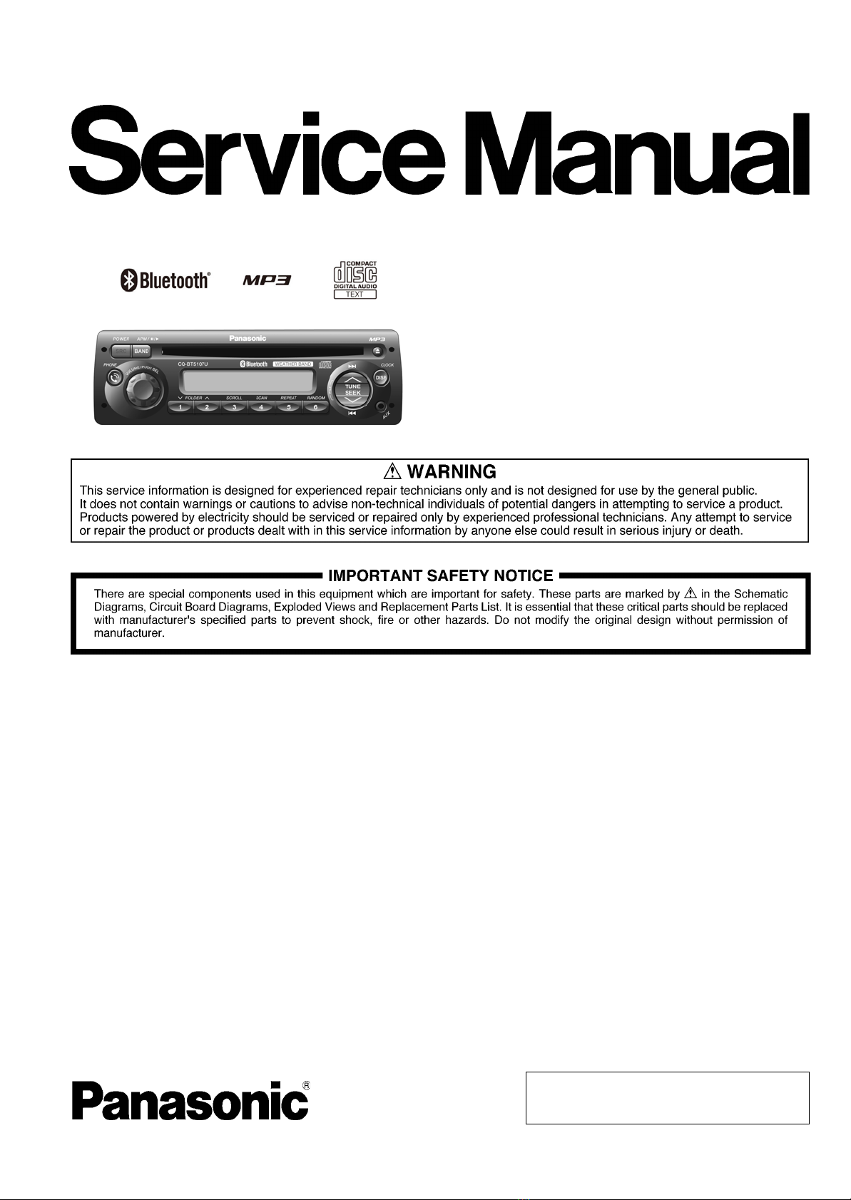
Panasonic CQBT-5107-U Service manual
ORDER NO.ACED101002CE
C1
AUTOMOTIVE AFTERMARKET
Model No. CQ-BT5107U
MP3 CD Player/Weather Band Receiver
with Built-in Bluetooth
TABLE OF CONTENTS
PAGE PAGE
1 Service Navigation----------------------------------------------- 2
2 Specifications ----------------------------------------------------- 3
3Features------------------------------------------------------------- 4
4 Technical Descriptions----------------------------------------- 5
5 Block Diagram----------------------------------------------------15
6 Wiring Connection Diagram ---------------------------------16
7 Schematic Diagram---------------------------------------------17
8 Schematic Diagram---------------------------------------------20
9 Printed Circuit Board-------------------------------------------21
10 Exploded View and Replacement Parts List -----------25
11 Schematic Diagram for Printing with Letter Size-----34
© Panasonic Corporation 2010.
Unauthorized copying and distribution is a
violation of law.
1 Service Navigation
1.1. About Lead Free Solder(PbF)
Distinction of PbF PCB
• PCBs(manufacture)using lead free solder will have a PbF
stamp on the PCB.
Caution
• Pb free solder has a higher melting point than standard solder; Typically the melting point is 50 - 70°F (30 - 40°C)
higher. Please use a soldering iron with temperature control
and adjust it to 700 ± 20°F (370 ± 10°C). In case of using
high temperature soldering iron, please be careful not to
heat too long.
• Pb free solder will tend to splash when heated too high
(about 1100°F/600°C)
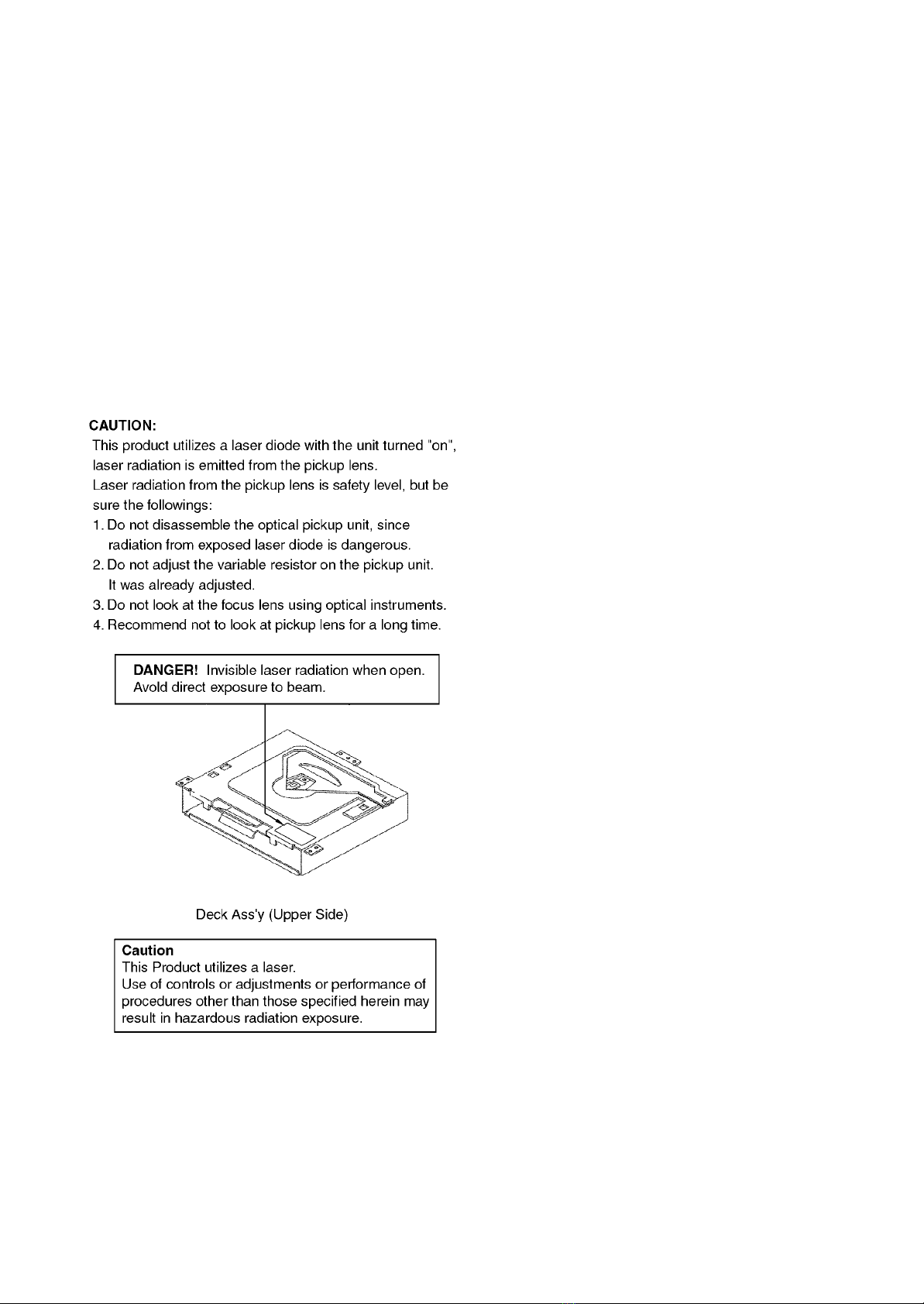
1.2. Laser Products
1.4. Maintenance
Your products is designed and manufactured to ensure a minimum of maintenance. Use a dry, a soft cloth for routine exterior
cleaning. Never use benzine, thinner or other solvents.
1.5. Notes
[RADIO BLOCK]
Do not align the AM/FM package block. When the package
block is necessary, it will be supplied already aligned at the factory.
[CD DECK BLOCK]
This model has no servo alignment points because microcomputer controls the servo circuit.
1.3. Replacing the Fuse
Use fuses of the same specified rating (15A). Using different
substitutes or fuses with higher ratings, or connecting the product directly without a fuse, could cause fire or damage to the
stereo unit.
2
2 Specifications
2.1. Specfications
General
Power Supply :
Current Consumption : Less than 2.5 A (CD mode, 0.5 W
Maximum Power Output :
Tone adjustment range : Bass:± 12 dB at 100 Hz
Power Output :
Suitable Speaker Impedance : 4-8Ω
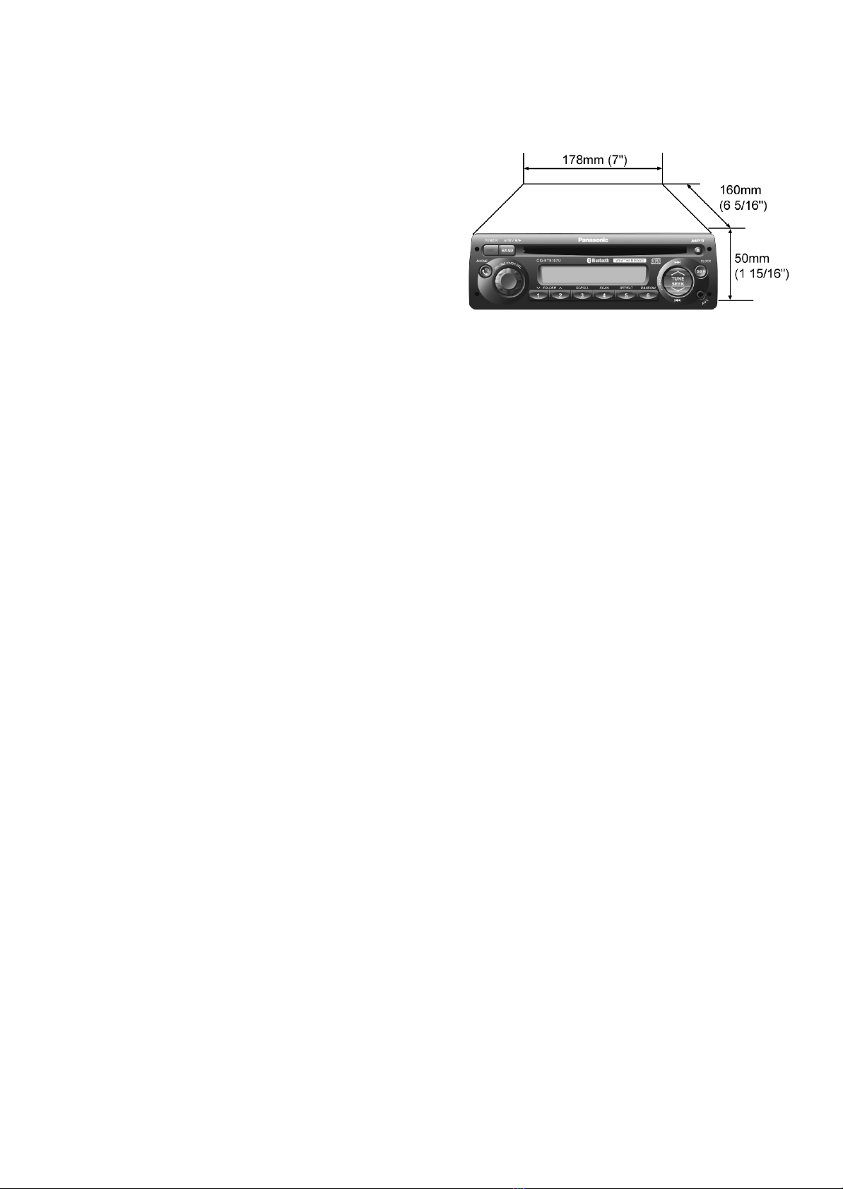
Dimensions (W x H x D)** : 178(W)×50(H)×160(D) mm {7” x 1-
Weight** : 1.4 kg {3 Ibs. 1 oz.}
Front AUX Input
Input impedance : 10 kΩ
Maxium input level : 2.0 V
Connector : 3.5 mm stereo mini pin
Input sensitivity : 200 mVrms
12 V DC (11 V - 16 V),
Test Voltage 14.4 V,Negative
ground
4-speaker)
45 W×4channels at 400 Hz, Volume Control Maximum.
Treble:± 12 dB at 10 kz
18 W per channel into 4
30,000 Hz at 3 % THD
15/16” x 6-5/16”}
Ω, 40 to
* Specifications and the design are subject to modification without
notice due to improvements in technology.
** Dimensions and Weight shown are approximate.
2.2. Dimensions
FM Stereo Radio
Frequency Range : 87.9 - 107.9 MHz
Usable Sensitivity : 12 dBf. (1.1 μV/ 75 Ω, S/N 30 dB)
50 dB Quieting Sensitivity : 17 dBf. (1.8 μV/ 75 Ω)
Frequency Response : 30-15,000 Hz ± 3 dB
Alternate Channel Selectivity : 75 dB
Stereo Separation : 35 dB at 1 kHz
Signal/Noise Ratio : 70 dB (Mono)
AM Radio
Frequency Range : 530 kHz - 1710 kHz
Usable Sensitivity : 28 dB/μV (25μV, S/N 20 dB)
Weather Band Radio
Frequency range : 162.400 - 162.550 MHz
Usable sensitivity : 3 dB (S/N 20 dB)
Signal/Noise Ratio (40 dB/μV) : 50 dB
CD Player
Sampling Frequency : 8 times oversampling
DA Converter : 1 bit DAC System
Pick-Up Type : Astigma 3-beam
Light Source : Semiconductor Laser
Wavelength : 790 nm
Frequency Response : 20 - 20,000 Hz (±1 dB)
Signal to Noise Ratio : 96dB
Wow and Flutter : Below measurable limits
Channel Separation : 75 dB
Bluetooth
Communication Frequency : 2,402 MHz - 2,480 MHz
Number of Channels : 79 Channels
Communication Mode : Frequency Hopped Spread Spec-
trum Communication
RF Output : 0 dBm (0.8mW)
Service Area : Within 10 m
Applicable Bluetooth Version : Version 2.1 + EDR
3

3 Features
• Front AUX terminal.
• Sound control.
• Bluetooth.(Music player,Handsfree,Phone book transfer,Voice dial)
• Alarm.
4
4 Technical Descriptions
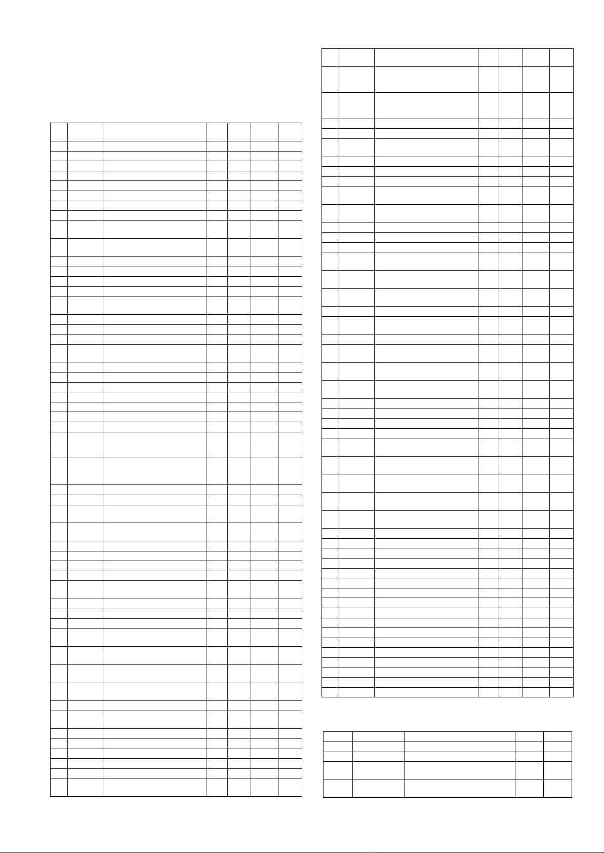
4.1. Main Block
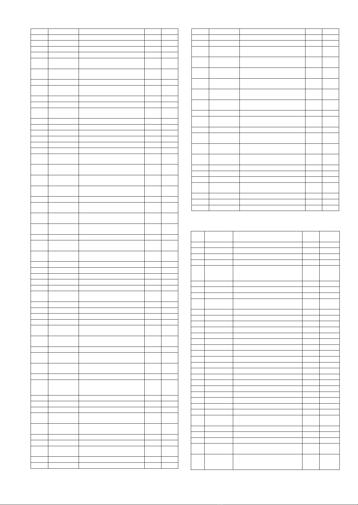
IC601:C2BBYY000892
Pin.
Port Description I/O FM(V) CD(V) BT(V)
No.
1 DBGP0 On chip debug port0. - 0 0 0
2 DBGP1 On chip debug port1. - 0 0 0
3 DBGP2 On chip debug port2. - 0 0 0
4 N.C. Not connected. O 0 0 0
5 N.C. Not connected. O 0 0 0
6 N.C. Not connected. O 0 0 0
7 N.C. Not connected. O 0 0 0
8 RESET Reset signal input. I 5.11 5.13 5.11
9 XT1 Main crystal 1 (32.768KHz) con-
10 XT2 Main crystal 2 (32.768KHz) con-
11 VSS GND - 0 0 0
12 CF1 Crystal (13.5MHz) connected. I 2.41 2.48 2.46
13 CF2 Crystal (13.5MHz) connected. O 2.25 2.46 2.6
14 VDD VDD +5V - 5.11 5.13 5.11
15 N.C.(INIT
_A)
16 N.C. Not connected. O 0 0 0
17 N.C. Not connected. O 0 0 0
18 N.C. Not connected. O 0 0 0
19 N.C.(INIT
_C)
20 N.C. Not connected. O 0 0 0
21 MODE_B Rotary clock signal B input. I 3.95 4.05 3.96
22 MODE_A Rotary clock signal A input. I 3.92 4.01 3.94
23 LCD_DI LCD data output. O 4.97 4.99 4.97
24 LCD_DO LCD data input. I 4.79 4.81 4.79
25 LCD_CLK LCD clock signal output. O 4.97 4.99 4.97
26 N.C. Not connection. O 0 0 0
27 EXT_RO
M_I2C_S
DA
28 EXT_RO
M_I2C_S
CL
29 LCD_CE
30 N.C. Not connection. O 0 0 0
31 CD_EM(L
M+)
32 CD_LM(L
M-)
33 CD_SW1 CD insert detection SW 1. I 5.04 0 5.09
34 CD_SW2 CD Mechanism SW 2. I 5.04 5.11 5.09
35 N.C. Not connection. O 0 0 0
36 CD_S/L CD connected detection. O 5.11 5.13 5.11
37 CD_DMUTECD motor driver IC action con-
38 N.C. Not connection. O 0 0 0
39 VSS GND - 0 0 0
40 VDD VDD +5V - 5.11 5.14 5.12
41 CD_MUTECD DSP mute detection. I 0.11 0.13 0
42 SUB_RE
ADY
43 REG_RE
ADY
44 CD_LIMIT
_SW
45 N.C. Not connection. O 0 0 0
46 CD_RESETCD DSP reset control signal. O 5.07 5.09 5.07
nected.
nected.
Not connected. I 5.03 5.11 5.05
Not connected. I 0 0 0
I2C data input/output for storing
BT information.
I2C clock output for storing BT
information.
LCD chip enable.
CD eject control signal. O 0 0 0
CD loading control signal. O 0 0 0
trol signal.
CD DSP communication
detection 1.
CD DSP communication
detection 2.
CD limit detection SW. I 4.86 0 4.92
I 1.42 1.44 1.46
O 2.18 2.21 2.18
I/O 5.11 5.13 5.11
O 5.11 5.13 5.11
O0 0 0
O0 0 0
I 4.86 4.95 4.93
I 4.87 4.95 4.93
Pin.
Port Description I/O FM(V) CD(V) BT(V)
No.
53 E-
VOL_I2C
_SDA
54 E-
VOL_I2C
_SCL
55 VDD VDD +5V - 5.11 5.13 5.11
56 VSS GND - 0 0 0
57 RADIO_WCRadio Tuner EEPROM write
58 N.C. Not connected. O 0 0 0
59 N.C. Not connected. O 0 0 0
60 N.C. Not connected. O 0 0 0
61 RADIO_R
ESET
62 RADIO_M
ODE
63 N.C. Not connected. O 0 0 0
64 BEEP Alarm function control. O 0 0 0
65 N.C. Not connected. O 0 0 0
66 BATT Battery power connected signal
67 RDS_INT
_CNT
68 AMP_STBAmp standby signal output. O 5.11 5.13 5.11
69 N.C. Not connected. O 0 0 0
70 AMP_MUTEAMP_MUTE control signal out-
71 N.C. Not connected. O 0 0 0
72 ACC ACC power connected signal
73 RADIO_I2
C_SDA
74 RADIO_I2
C_SCL
75 BT_RX BT data send output. O 3.31 3.33 3.31
76 BT_TX BT data received input. I 3.32 3.34 3.31
77 N.C. Not connected. O 0 0 0
78 N.C. Not connected. O 0 0 0
79 POWER_
CNT
80 N.C.(ANT
_CNT)
81 AMP_CNTAMP control signal output. O 5.13 5.11 5.11
82 AF_MUTEAF MUTE control signal output. O 5.13 0 5.11
83 BT_RESETBT module reset signal output. O 3.29 3.29 3.29
84 N.C. Not connected. O 0 0 0
85 N.C. Not connected. O 0 0 0
86 N.C. Not connected. O 0 0 0
87 VREG Bypass condenser connected. O 4.44 4.41 4.41
88 VSS GND - 0 0 0
89 VDD(PLL) VDD +5V - 5.13 5.11 5.11
90 N.C. Not connected. I 0 0 0
91 N.C. Not connected. I 0 0 0
92 N.C. Not connected. I 0 0 0
93 N.C. Not connected. I 0 0 0
94 EO1 Main charge pump output. O 0 0 0
95 SUBFD Sub charge pump output. O 0 0 0
96 N.C. Not connected. O 0 0 0
97 N.C. Not connected. O 0 0 0
98 N.C. Not connected. O 0 0 0
99 N.C. Not connected. O 0 0 0
100 N.C. Not connected. O 0 0 0
Electronic Vol-IC data output. O 5.11 5.13 5.11
Electronic Vol-IC clock output. O 5.11 5.13 5.11
control.
Radio reset output pin. O 3.1 3.25 3.23
Radio power control signal. O 5.09 5.11 5.09
detection. (H-ON, L-OFF)
Radio Tuner I2C address selec-
tion.
put.
detection.
Radio Tuner data input/output. I/O 3.23 3.3 3.28
Radio Tuner clock output. O 2.79 3.3 3.31
Power IC control signal output. O 5.11 5.12 5.11
Not connected. O 0 0 0
O 3.3 3.33 3.31
I 4.85 4.92 4.9
O 3.05 3.08 3.07
O5.11 0 5.11
I 4.95 4.96 4.95
IC401:C5ZBZ0000069
47 N.C. Not connection. O 0 0 0
48 N.C. Not connection. O 0 0 0
49 CD_DI CD DSP data output. O 0 0 0
50 CD_DO CD DSP data input. I 3.32 3.34 3.32
51 CD_CLK CD DSP clock signal output. O 0 0 0
52 CD_CE CD DSP chip enable control sig-
nal.
O0 0 0
Pin No. Port Description I/O (V)
1 EFMIN RF signal input port. I 1.58
2 RFOUT RF signal output port. O 1.67
3 LPF LPF capacitor connection port for
4 PHLPF LPF capacitor connection port for
RF DC level detection.
detection.
5
O1.64
O1.68
Pin No. Port Description I/O (V)
5 AIN A signal input port. I 1.66
6 CIN C signal input port. I 1.66
7 BIN B signal input port. I 1.66
8 DIN D signal input port. I 1.66
9 FEC LPF capacitor connection port for
10 RFMON LSI build-in analog signal monitor
11 VREF VREF voltage output port. O 1.66
12 JITTC Capacitor connection port for JIT
13 EIN E signal input port. I 1.65
14 FIN F signal input port. I 1.66
15 TEC LPF capacitor connection port for
16 TE TE signal output port. O 1.57
17 TEIN TE signal input port for TES. I 1.65
18 LDD Laser power detection output port. O 3.27
19 LDS Laser power detection input port. I 0
20 AVSS GND for analog. - 0
21 AVDD VDD for analog. - 3.27
22 FDO Focus control signal output port.
23 TDO Tracking control signal output port .
24 SLDO Thread control signal output port.
25 SPDO Spindle control signal output port.
26 VVSS 1 Gnd for build - i n VCO. - 0
27 PDOUT1 Phase comparison output port1 for
28 PDOUT0 Phase comparison output port0 for
29 PCKIST PDOUT01 output port for current
30 VVDD1 VDD for VCO. - 3.29
31 DMUTEB DMUTEB (GENERAL) output
32 PUIN PUIN (GENERAL) I/O port.Built-in
33 DEFFCT Detection signal output port. O 0
34 FSEQ Synchronous signal output port. - 0
35 C2F C2 error signal output port. O 0
36 DVDD VDD for Digital. - 3.29
37 DVSS GND for Digital. - 0
38 DVDD18 VDD capacitor connection port for
39 MONI 0 Monitor port 0. O 0
40 MONI 1 Monitor port 1. O 0
41 DVDD VDD for Digital. - 3.25
42 DVSS GND for Digital. - 0
43 CE Host IF:Communication enable
44 CL Host IF:Data transfer clock input
45 DI Host IF:Data input port. I 3.6
46 DO Host IF:Data output port.Pull-up is
47 RESB "Reset input port.Make it ""L""
48 INTB Interrupt signal output port.(Servo) O 3.25
49 SUB_READY 0 For host u-com IF:SUB-RDY out-
50 CD_MUTE 0 General I/O port2. I/O 5.31
51 LOW_BATI Ge ne r a l I/O port1. I/O 5.16
52 CONT General I/O port0. I/O 0
53 OSCCNT OSCOFF control port.Connected
54 STREQ Stream data demand signal output
55 STCK Clock input port for stream data. I/O 0
56 STDATA Stream data input port. I/O 0
57 TEST 1 Input port for test.Needed con-
58 DATA Lch/Rch data output port. O 0
59 DATACK Clock output port. O 0
FE signal.
port.
signal.
TE signal.
D/A output.
D/A output.
D/A output.
D/A output.
build-in VCO control.
build-in VCO control.
setting.
port.
pull-up resistance.
digital circuit.
signal input port.
port.
necessary.
when power on."
put.Pull-up resistance is necessary.
with 0V when reset.
port.
nect with 0V.
O1.6
O1.64
O0
O1.57
O1.65
O1.65
O1.64
O1.64
O0
O0
I1.07
O0
I/O 0
O1.83
I3.6
I3.7
O3.3
I0
O0
I0
I/O 0
I0
Pin No. Port Description I/O (V)
60 LRSY Lch/Rch clock output port. O 0
61 VVDD 2 VDD for build-in VCO. - 3.25
62 VPREF 2 Built-in VCO oscillation cooking
63 VCOC 2 Built-in VCO control voltage set-
64 VPDOUT 2 Output port for built-in VCO con-
65 VVSS 2 GND for building VCO. Needed
66 DVDD18 VDD capacitor connection port for
67 DVSS GND for digital system. Needed
68 DVDD VDD for digital system. - 3.25
69 DOUT Digital OUT output port. EIAJ for-
70 AMUTEB AMUTEB (general) ouput port. O 0
71 XVSS GND for oscillation circuit. Needed
72 XOPUT Connected of 16.9344MHz oscilla-
73 XIN Connected of 16.9345MHz oscilla-
74 XVDD VDD for oscillation circuit. I 3.19
75 LCHO L channel output port. O 0
76 LRVDD VDD for LR channel. - 3.21
77 LRVSS GND for LR channel. Needed con-
78 RCHO R channel output port. O 0
79 AVDD VDD for analog. - 3.27
80 SLCO Slice level control output port. O 1.6
stove setting input terminal.
ting input port.
trol.
connect with 0V.
digital circuit.
connect with 0V.
mat.
connect with 0V.
tion.
tion.
nect with 0V.
I3.25
I1.08
O0.08
-0
O1.84
-0
O0
-0
O1.39
I1.35
-0
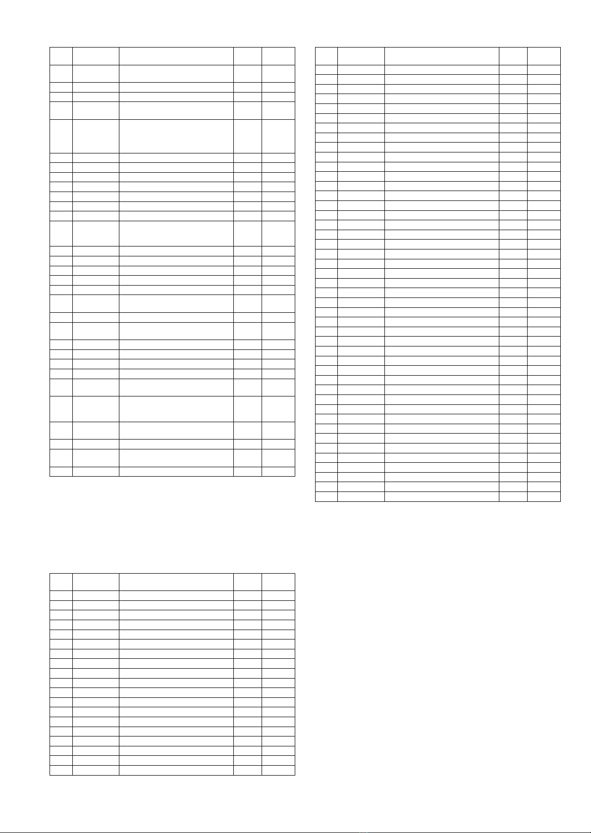
IC100:J3FYY0000014
Pin.
No.
PORT Description I/O (V)
1 UART_CTS UART clear to send active low. I 0
2 UART_RTS UART request to send active low. O 0
3 UART_RX UART data input. I 3.8
4 UART_TX UART data output. O 3.32
5 VREGIN_L Input to internal low-voltage linear
6 VDD_MEM VDD VDD 3.32
7 VDD_PIO VDD VDD 3.32
8 GND Ground GND 0
9 RESET# CMOS input with weak internal pull-
10 PIO[10] Programmable input/output line. O 0
11 PIO[9] Programmable input/output line. O 0
12 PIO[15] Programmable input/output line. O 0
13 PIO[11] Programmable input/output line. O 0
14 PIO[12] Programmable input/output line. O 0
15 PIO[13] Programmable input/output line. O 0
16 PIO[14] Programmable input/output line. O 0
17 PIO[8] Programmable input/output line. O 0
18 PIO[7] Programmable input/output line. O 0
19 PIO[6] Programmable input/output line. O 0
20 PIO[5] Programmable input/output line. O 0
21 PIO[4] Programmable input/output line. O 0
22 PCM_IN Synchronous data input. I 0
23 PCM_CLK Synchronous data clock. O 0
24 PCM_OUT Synchronous data output. O 0
25 PCM_SYNC Synchronous data sync. O 0
26 SPI_MOSI SPI data input. I 0
27 SPI_CLK SPI clock. I 0
28 SPI_CSB Chip select for Serial Peripheral
29 SPI_MISO SPI data output. O 0
30 LED[0] LED driver. O 0
31 LED[1] LED driver. O 0
32 VREGIN_H Input to internal high-voltage linear
33 VREGEN_H Take high to enable high-voltage
regulator for non-audio core
circuity.(1.8V-2.7V)
up.
Interface (SPI), active low.
regulator. (2.5V-4.9V)
linear regulator and switch-mode
regulator.
I1.88
I3.29
I3.14
I0
I3.3
6
Pin.
No.
PORT Description I/O (V)
34 VREGOUT_H High-voltage linear regulator output.
35 N.C. Not connection. O 0
36 GND Digital Ground. GND 0
37 VDD_CHG Lithium ion/polymer battery charger
38 VDD_BAT Lithium ion/polymer battery positive
39 GND Digital Ground. GND 0
40 MIC_BIAS Microphone bias. I 0
41 MIC_R_P Micropho ne input positive,right. I 0
42 MIC_R_N Microphine input negative,right. I 0
43 MIC_L_P Microphone input positive,left. I 0
44 MIC_L_N Microphone input negative,left. I 0
45 AGND Analogue Ground. GND 0
46 VDD_AUDIO Positive supply output for audio
47 SPK_R_N Speaker output negative,right. O 0.72
48 SPK_R_P Speaker output positive,right. O 0.72
49 SPK_L_N Speaker output negative,left. O 0.71
50 SPK_L_P Speaker output positive,left. O 0.71
51 PIO[3] Programmable input/output line. O 0
52 PIO[1] Programmable input/output line.
53 PIO[2] Programmable input/output line. O 0
54 PIO[0] Programmable input/output line.
55 GND Digital Ground. GND 0
56 GND Digital Ground. GND 0
57 ANT RF out. O 0
58 GND Digital Ground. GND 0
59 AIO[0] Analogue programmable input/out
60 VDD_ANA Positive supply output for analogue
61 AIO[0] Analogue programmable input/
62 GND Digital Ground. GND 0
63 USB_DP USB data plus with selectable
64 USB_DN USB data minus. I 0
(1.8V out)
input. (4.5V-6.5V)
terminal.Battery charger output and
input to switch-mode regulator.(4.2V
out)
circuitry and 1.5V regulated output.
(from internal low-voltage regulator)
(external TXEN)
(external RXEN)
line.
circuitry and 1.5V regulated output.
(from internal low-voltage regulator)
output line.
internal 1.5kΩ pull-up resistor.
O1.89
I0
O0
O1.47
O0
O0
O0
O0
O0
I0
Note 1 :
Voltage measuerments are with respect to ground, with a
voltmeter (internal resistance : 10M
Ω).
Pin.
No.
PORT Description I/O (V)
20 S20 Segment outputs. O 2.58
21 S21 Segment outputs. O 2.58
22 S22 Segment outputs. O 2.58
23 S23 Segment outputs. O 2.58
24 S24 Segment outputs. O 2.58
25 S25 Segment outputs. O 2.58
26 S26 Segment outputs. O 2.58
27 S27 Segment outputs. O 2.58
28 S28 Segment outputs. O 2.58
29 S29 Segment outputs. O 2.58
30 S30 Segment outputs. O 2.58
31 S31 Segment outputs. O 2.58
32 S32 Segment outputs. O 2.58
33 S33 Segment outputs. O 2.58
34 S34 Segment outputs. O 2.58
35 S35 Segment outputs. O 2.58
36 S36 Segment outputs. O 2.58
37 S37 Segment outputs. O 2.58
38 S38 Segment outputs. O 2.58
39 COM4 Common driver outputs. O 2.58
40 COM3 Common driver outputs. O 2.58
41 COM2 Common driver outputs. O 2.58
42 COM1 Common driver outputs. O 2.58
43 S40 Segment outputs. O 2.58
44 KS2 Key scan outputs. O 5.17
45 KS3 Key scan outputs. O 5.17
46 KS4 Key scan outputs. O 5.17
47 KS5 Key scan outputs. O 5.17
48 KS6 Key scan outputs. O 5.17
49 KI1 Key scan inputs. I 0.1
50 KI2 Key scan inputs. I 0
51 KI3 Key scan inputs. I 0
52 KI4 Key scan inputs. I 0
53 KI5 Key scan inputs. I 0
54 VDD Logic block power supply. - 3.3
55 VLCD LCD driver block power supply. - 5.18
56 VLCD1 LCD drive bias voltage. - 3.4
57 VLCD2 LCD drive bias voltage. - 1.72
58 VSS Ground. - 0
59 TEST Must be connected to ground. I 0
60 OSC Oscillator circuit port. I/O 2.3
61 DO Output data. O 3.3
62 CE Chip enable. I 0
63 CL Synchronization clock. I 2.7
64 DI Transfer data. I 2.6
4.2. Display Block
IC901:C0HBA0000246
Pin.
No.
PORT Description I/O (V)
1 P1 General-purpose output. O 5.1
2 P2 General-purpose output. O 0
3 P3 General-purpose output. O 0
4 S4 Segment outputs. O 2.58
5 S5 Segment outputs. O 2.58
6 S6 Segment outputs. O 2.58
7 S7 Segment outputs. O 2.58
8 S8 Segment outputs. O 2.58
9 S9 Segment outputs. O 2.58
10 S10 Segment outputs. O 2.58
11 S11 Segment outputs. O 2.58
12 S12 Segment outputs. O 2.58
13 S13 Segment outputs. O 2.58
14 S14 Segment outputs. O 2.58
15 S15 Segment outputs. O 2.58
16 S16 Segment outputs. O 2.58
17 S17 Segment outputs. O 2.58
18 S18 Segment outputs. O 2.58
19 S19 Segment outputs. O 2.58
7
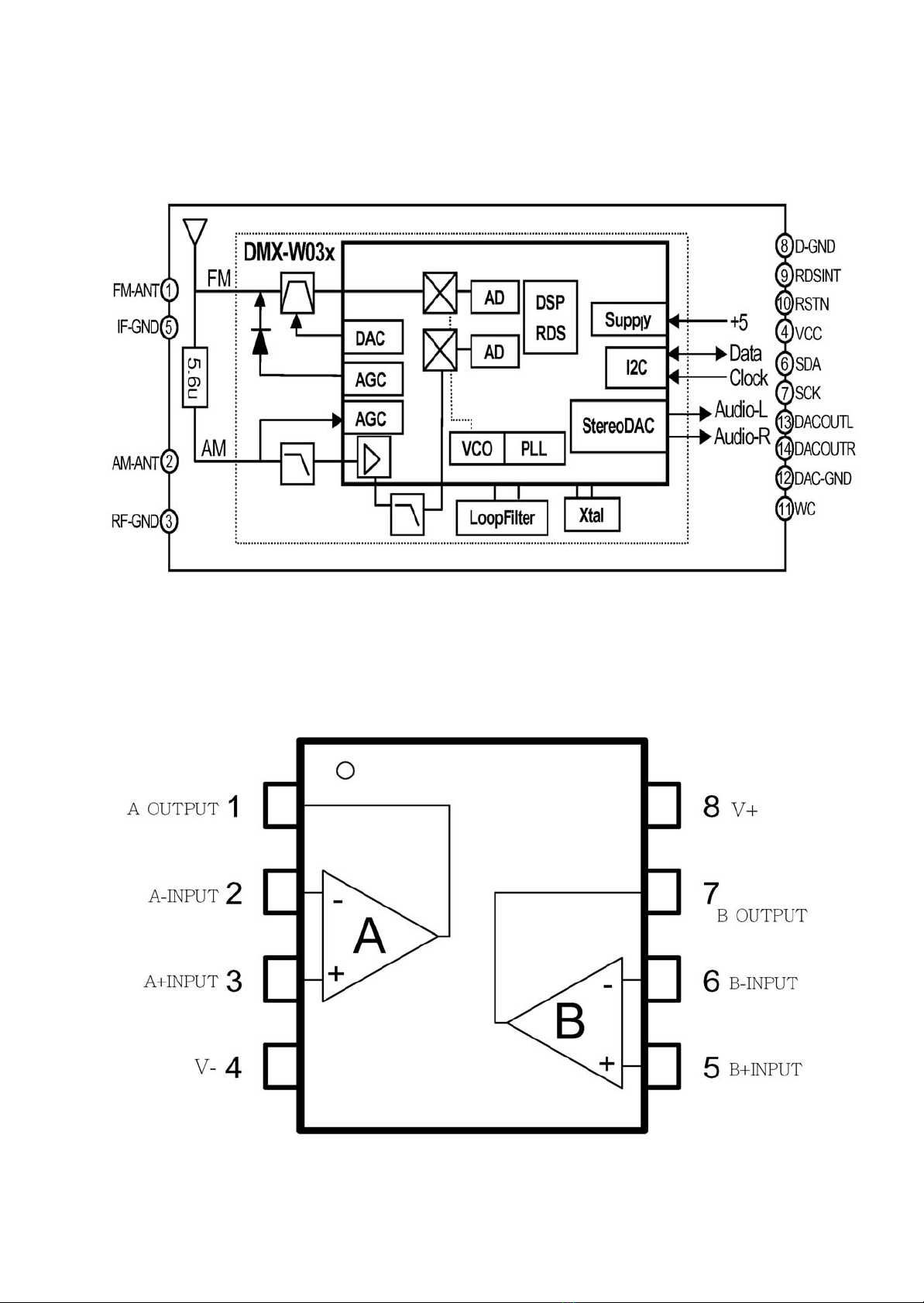
4.3. IC Block Diagram
4.3.1. Main Block
PAC51:J3CZZZ000002
IC101:C0ABBB000179
8
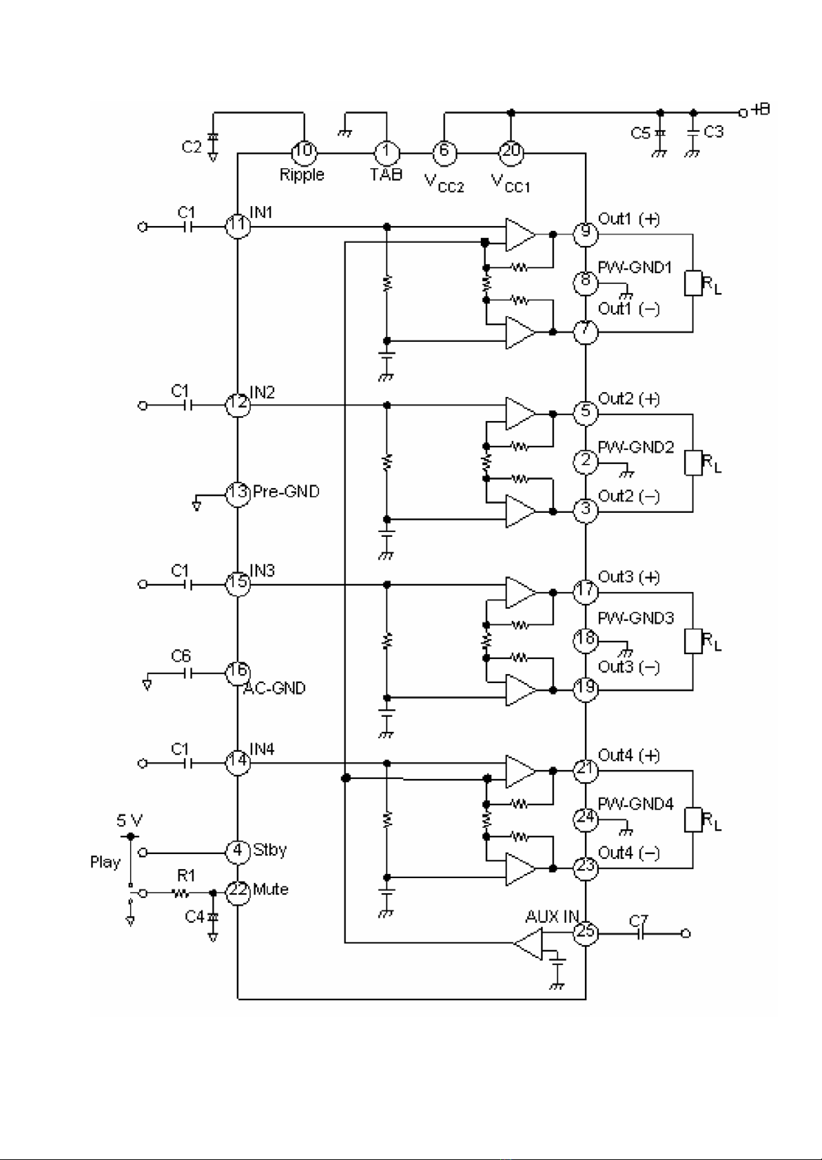
IC201:C1AA00000788
9
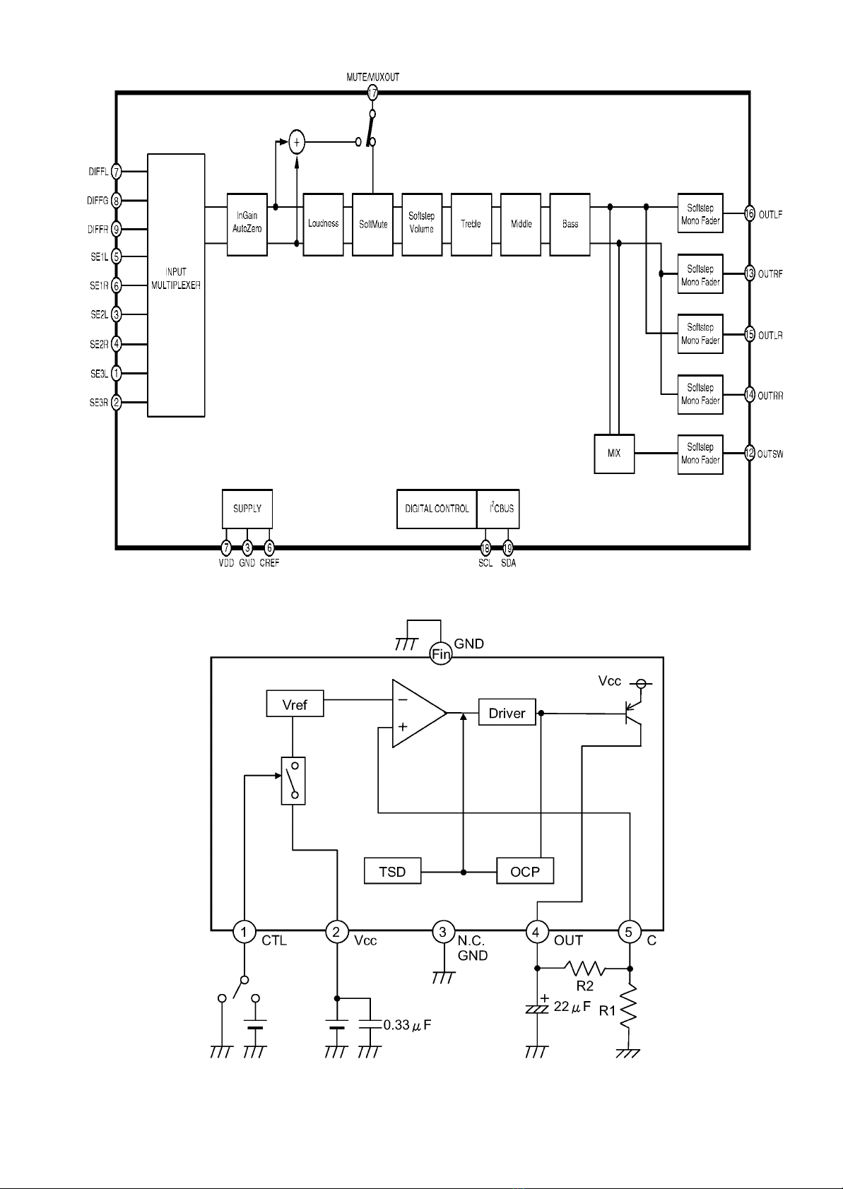
IC301:C1AB00002836
IC51:C0DBEJG00001
10
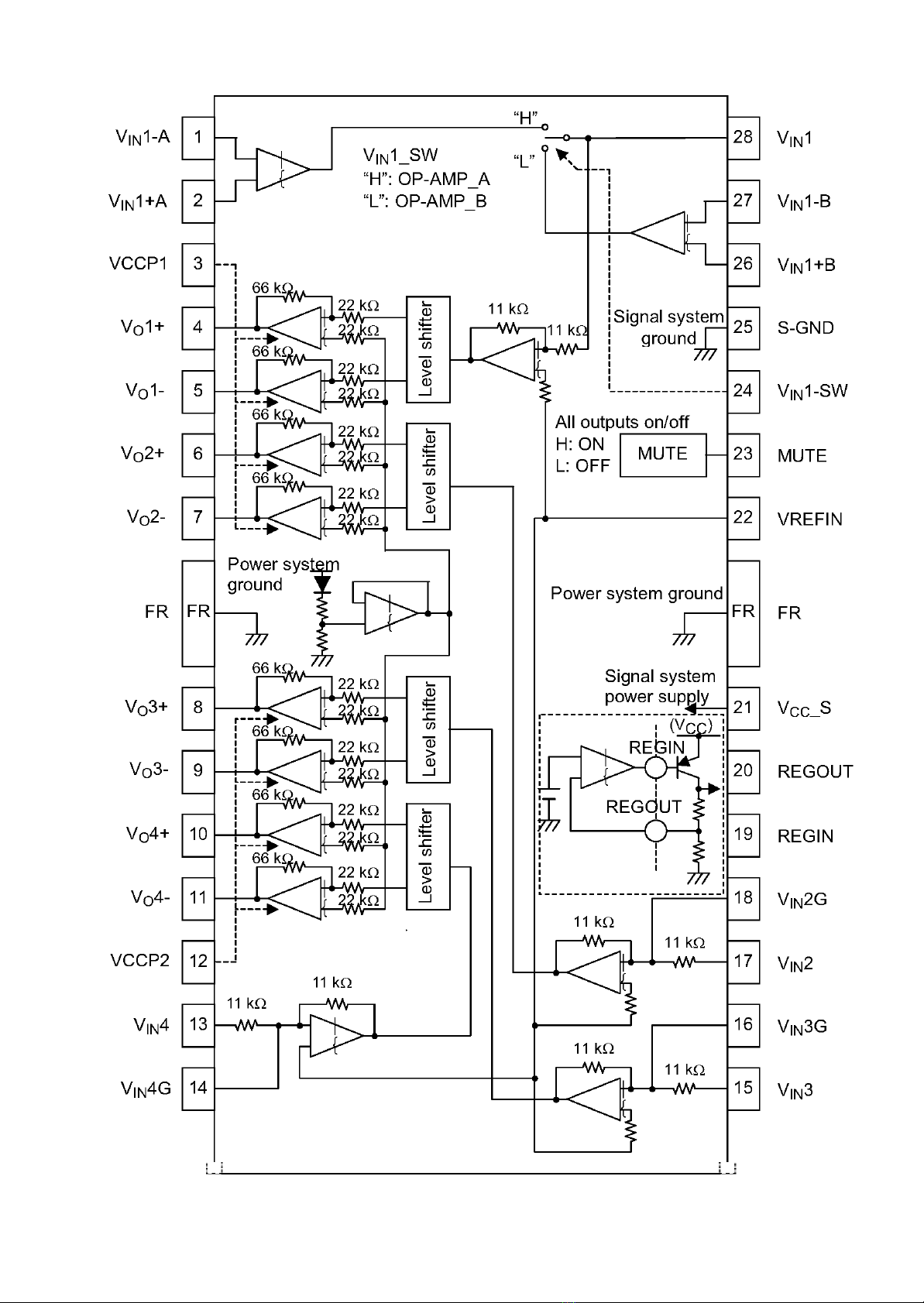
IC501:C1BB00001088
11
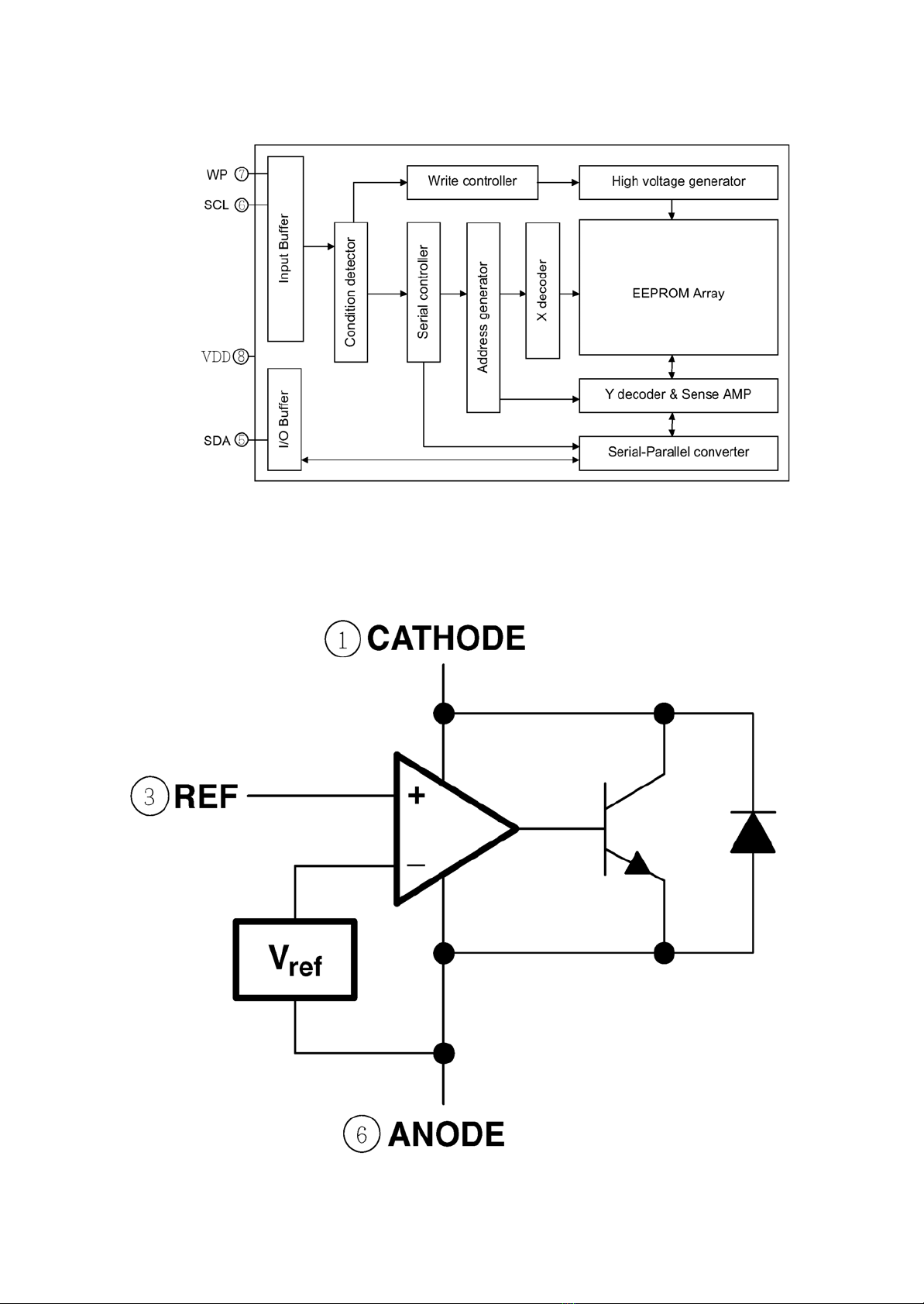
IC602:C3EBJY000032
IC702:C0DBEYY00005
12
 Loading...