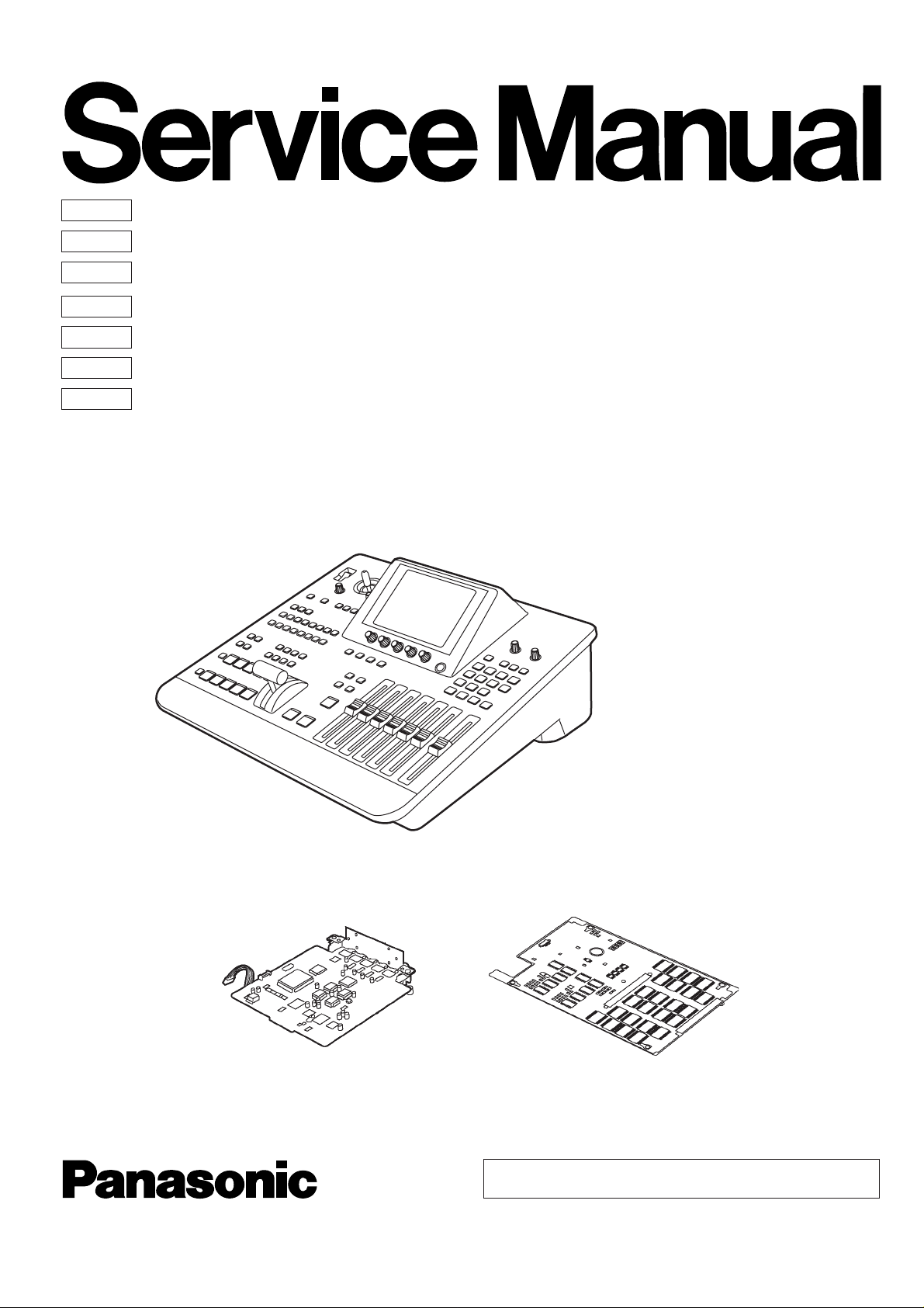
Panasonic AG-MX70 Service manual
ORDER NO. BSD0209M612
Sec. 1
Sec. 2
Sec. 3
Sec. 4
Sec. 5
Sec. 6
Sec. 7
Service Information
Disassembly Procedures
Electrical Adjustments
Block Diagrams
Schematic Diagrams
Circuit Board Diagrams
Exploded Views &
Replacement Parts Lists
Digital AV Mixer
AG-MX70E/MC
SD INTERFACE BOARD
AG-YA70P
3D EFFECT BOARD
AG-VE70P
AG-YA70P
AG-MX70E/MC
AG-VE70P
© 2002 Matsushita Electric Industrial Co., Ltd. All rights reserved.
Unauthorized copying and distribution is a violation of law.
WARNING
This service information is designed for experienced repair technicians only and is not designed for use by the general public.
It does not contain warnings or cautions to advise non-technical individuals of potential dangers in attempting to service a product.
Products powered by electricity should be serviced or repaired only by experienced professional technicans. Any attempt to service or rep air
the product or products deal with in this service manual by anyone else could result in serious injury or death.
AG-MX70E/MC
- 1-
-
2
-
- 3-
AG-YA70P
AG-VE70P
-
4
-
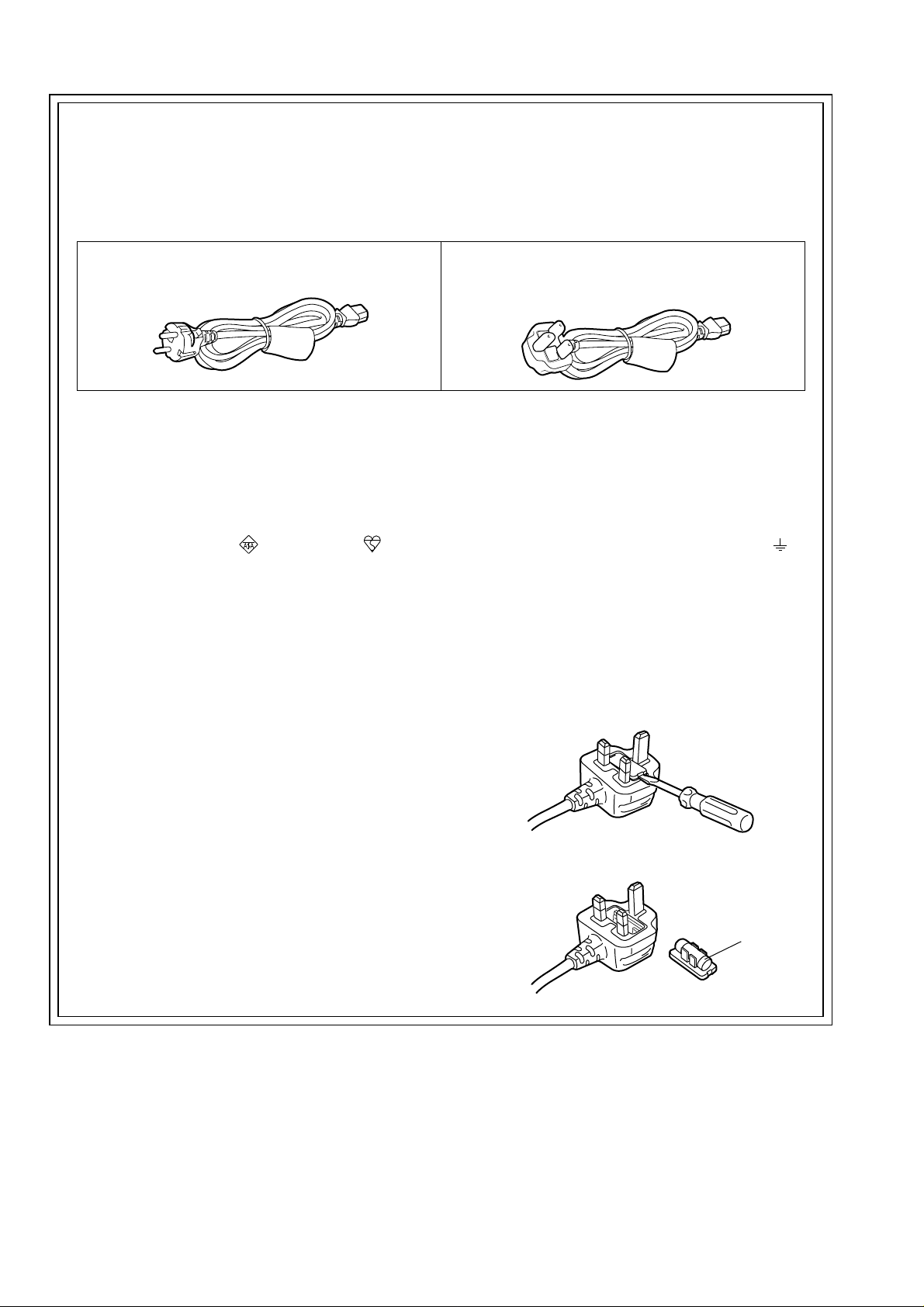
Caution for AC Mains Lead
FOR YOUR SAFETY PLEASE READ THE FOLLOWING TEXT CAREFULLY.
This product is equipped with 2 types of AC mains cable. One is for continental Europe, etc. and the other one is only for
U.K.
Appropriate mains cable must be used in each local area, since the other type of mains cable is not suitable.
FOR CONTINENTAL EUROPE, ETC.
Not to be used in the U.K.
FOR U.K. ONLY
This appliance is supplied with a moulded three pin
mains plug for your safety and convenience.
A 13 amp fuse is fitted in this plug.
Should the fuse need to be replaced please ensure that
the replacement fuse has a rating of 13 amps and that
it is approved by ASTA or BSI to BS1362.
Check for the ASTA mark or the BSI mark on the
body of the fuse.
If the plug contains a removable fuse cover you must
ensure that it is refitted when the fuse is replaced.
If you lose the fuse cover the plug must not be used
until a replacement cover is obtained.
A replacement fuse cover can be purchased from your
local Panasonic Dealer.
IF THE FITTED MOULDED PLUG IS UNSUITABLE
FOR THE SOCKET OUTLET IN YOUR HOME THEN
THE FUSE SHOULD BE REMOVED AND THE PLUG
CUT OFF AND DISPOSED OF SAFELY. THERE IS A
DANGER OF SEVERE ELECTRICAL SHOCK IF THE
CUT OFF PLUG IS INSERTED INTO ANY 13 AMP
SOCKET.
FOR U.K. ONLY
If the plug supplied is not suitable for your socket
outlet, it should be cut off and appropriate one fitted.
As the colours of the wires in the mains lead of this
appliance may not correspond with the coloured markings identifying the terminals in your plug, proceed as
follows:
The wire which is coloured GREEN-AND-YELLOW
•
must be connected to the terminal in the plug which is
marked with the letter E or by the Earth symbol or
coloured GREEN or GREEN-AND-YELLOW.
The wire which is coloured BLUE must be connected
•
to the terminal in the plug which is marked with the
letter N or coloured BLACK.
The wire which is coloured BROWN must be con-
•
nected to the terminal in the plug which is marked with
the letter L or coloured RED.
How to replace the fuse
1. Open the fuse compartment with a screwdriver.
If a new plug is to be fitted please observe the wiring
code as shown below.
If in any doubt please consult a qualified electrician.
WARNING: THIS APPLIANCE MUST BE EARTHED.
IMPORTANT: The wires in this mains lead are coloured
in accordance with the following code:
Green-and-Yellow:
Blue:
Brown:
Earth
Neutral
Live
2. Replace the fuse.
Fuse
- 5-
SAFETY PRECAUTIONS
GENERAL GUIDELINES
1. When servicing, observe the ori gin al l ead dre ss. If a short
circuit is found, replace all parts which have been overheated or damaged by the short circuit.
2. After servicing, see to it that all the protective devices
such as insulation barriers, insulation papers shields are
properly installed.
3. After servicing, make the following leakage current
checks to prevent the customer from being exposed to
shock hazards.
LEAKAGE CURRENT COLD CHECK
1. Unplug the AC cord and connect a jumper between the
two prongs on the plug.
2. Measure the resistance value, with an ohm meter,
between the jumpered AC plug and each exposed
metallic cabinet part on the equipment such as
screwheads, connectors, control shafts, etc. The
resistance value must be more than 5MΩ.
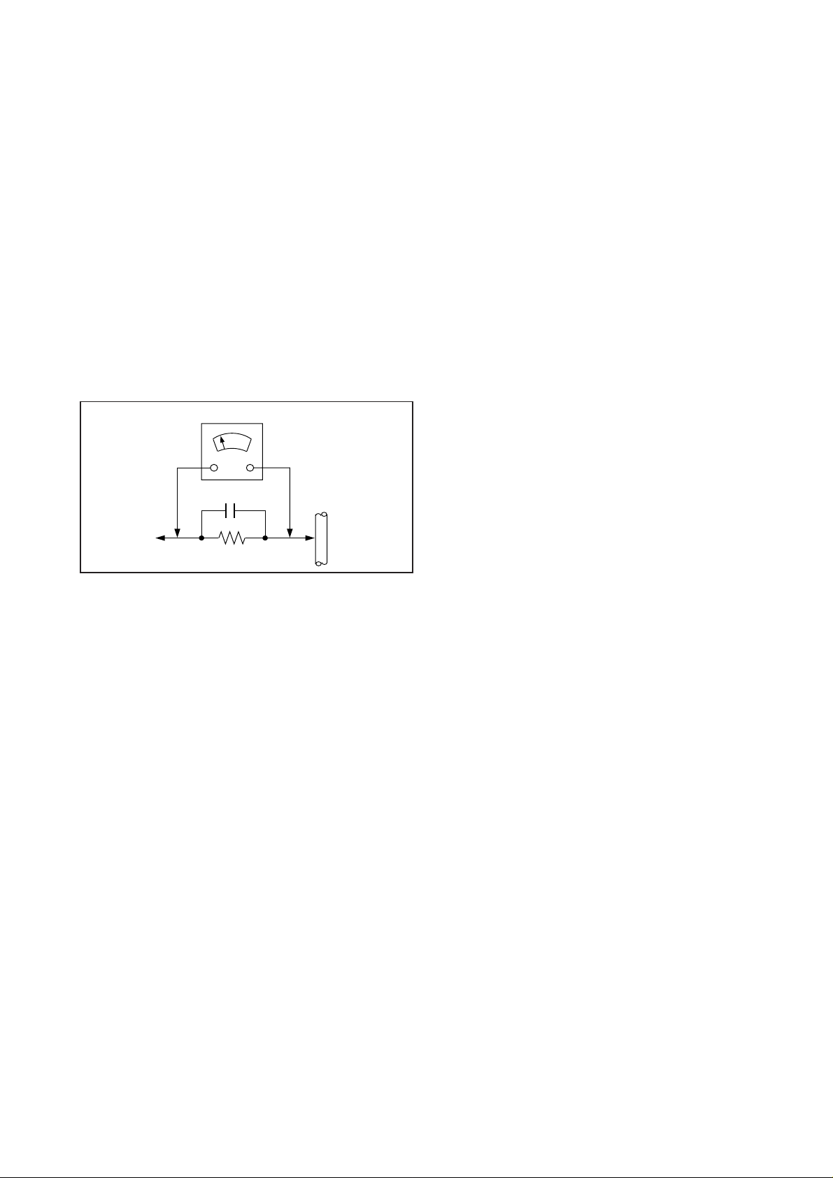
AC VOLTMETER
Hot-Check Circuit
COLD
WATER PIPE
(EARTH GROUND)
TO
APPLIANCES
EXPOSED
METAL PARTS
0.15µF
1500Ω
10W
Figure1
LEAKAGE CURRENT HOT CHECK (See Figure 1)
1. Plug the AC cord directly into the AC outlet.
Do not use an isolation transformer for this check.
2. Connect a 1.5kΩ , 10W resistor, in parallel with a 0.15µ
F capacitor, between each exposed metallic part on the
set an a good earth ground such as a water pipe, as
shown in Figure1.
3. Use an AC voltmeter, with 1000 ohms/volt or more
sensitivity, to measure the potential across the resistor.
4. Check each exposed metallic part, and measure the
voltage at each point.
5. Reverses the AC plug in the AC outlet repeat each of the
above measurements.
6. The potential at any point should not exceed 0.15 volts
RMS. A leakage current tester (Simpson Model 229
equivalent) may be use d to ma ke the hot checks, l eak age
current must not exceed 0.1 milliamp. In case a
measurement is outside of the limits specified, there is a
possibility of a shock hazard, and the equipment should
be repaired and rechecked before it is returned to the
customer.
ABOUT LEAD FREE SOLDER (PbF)
Distinction of Pbf PCB :
PCBs (manufactured) using lead free solder will have a Pbf
stamp on the PCB.
Caution :
1. Pb free solder has a high melting point than standerd
solder; Typically the melting point is 50-70˚F (30-40˚C)
higher. Please use a high temperature soldering iron. In
case of the soldering iron with temperature control,
please set it to 700±20˚F (370±10˚C).
2. Pb free solder will tend to splash when heated too high
(about 1100˚F/600˚C)
ELECTROSTATICALLY SENSITIVE (ES) DEVICES
Some semiconductor (solid state) devices can be damaged
easily by static electricity. Such components commonly are
called Electrostatically sensitive (ED) Devices. Examples of
typical ES devices are integrated circuits and some fieldeffect transistors and semiconductor “chip” components. The
following techniques should be used to help reduce the
incidence of component damage caused by static electricity.
1. Immediately before handling any semiconductor
component or semiconductor-equipped assembly, drain
off any electrostatic charge on your body by touching a
known earth ground.
Alternatively, obtain and wear a commercially available
discharging wrist trap device, which should be removed
for potential shock reasons prior to applying power to the
unit under test.
2. After removing an electrical assembly equipped with ES
devices, place the assembly on a conductive surface
such as aluminum foil, to prevent electrostatic charge
buildup or exposure of the assembly.
3. Use only a grounded tip soldering iron to solder or
unsolder ES devices.
4. Use only an anti-static solder re moval devic e clas sified as
“anti-static” can generate electrical charges sufficient to
damage ES devices.
5. Do not use freon-propelled chemicals. These can
generate electrical charges sufficient to damage ES
devices.
6. Do not remove a replacement ES device from its
protective package until immediately before you are
ready to install it.
(most replacement ES devices are package with leads
electrically shorted together by conductive foam,
aluminum foil or comparable conductive material).
7. Immediately before removing the protective material from
the leads of a replacement ES device, touch the
protective material to the chassis or circuit assembly into
which the device will be installed.
CAUTION : Be sure no power is applied to the chassis or
circuit, and observe all other safety precautions.
8. Minimize bodily motions when handling unpacked
replacement ES devices. (Otherwise harmless motion
such as the brushing together of y o ur c loth es f abri c or the
lifting of your foot from a carpeted floor can generate
static electricity sufficient to damage an ES device).
X-RADIATION
WARNING
1. The potential source of X-radiation in EVF sets is the
High Voltage section and the picture tube.
2. When using a picture tube test jig for service, ensure that
jig is capable of handling 10kV without causing xradiation.
Note :
3. Measure the High Voltage. The meter (electric type)
It is important to use an accurate periodically
calibrated high voltage meter.
reading should indicate 2.5kV, 0.15kV. If the meter
indication is out of tolerance, immediate service and
correction is required to prevent the possibility of
premature component failure. To prevent an x-radiation
possibility, it is essential to use the specified picture tube .
±
-
6
-

HCD0209NYAA425

SERVICE INFORMATION
CONTENTS
1. Equipment For Measurement ...............................................................................
2. Maintenance...........................................................................................................
2-1. Necessity For Maintenance...................................................................................................... INF-1
2-2. Maintenance Schedule............................................................................................................. INF-1
3. Up Dating The Software ........................................................................................
3-1. Software ................................................................................................................................... INF-2
3-2. Layout of parts ......................................................................................................................... INF-2
3-3. Preparations for updating the internal flash memory microprocessor ..................................... INF-3
3-4. Steps for updating the internal flash memory microprocessor................................................. INF-3
3-5. Updating the PLD (Altera) ........................................................................................................ INF-5
4. The way of attaching an option board .................................................................
4-1. Installation of the AG-YA70P ................................................................................................... INF-8
4-2. Installation of the AG-VE70P ................................................................................................... INF-10
INF-1
INF-1
INF-2
INF-8
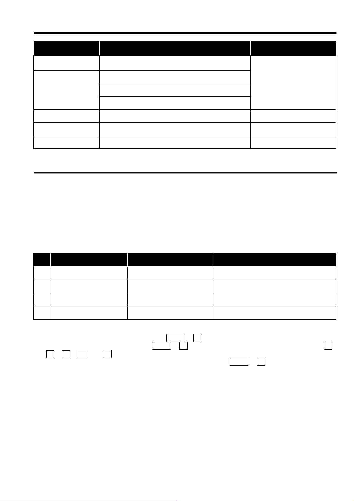
1. Equipment For Measurement
MODEL No.
(EXAMPLE)
TSG130
1760 or 1780R
PAL analog component/Composite signal
Transmitter
SCH meter (PAL)
Oscilloscope (PAL)
Vectorscope (PAL)
Audio analyzer
Digital voltmeter (D.V.M.)
Wave Frequency counter
NAME REMARKS
Techtronics
2. Maintenance
2-1. Necessity For Maintenance
The digital AVmixer has an fanmotor and LCD which are consumable items that deteriorate over time and can
cause lower performance and malfunction. You should, therefore, perform maintenance regularly to prevent
lower performance and potentially damaging malfunctions.
2-2. Maintenance Schedule
The following maintenance schedule shows approximate times to carry out maintenance. They are not the
performance lives of the various parts. There may be changes to the maintenance specifications and part
numbers so be sure to refer to the latest information.
No. PART PART NUMBER TIME FOR REPLACEMENT
1 Top case fan motor L6FALEDH0001 every ten thousand hours
2 Main case fan motor L6FALEDH0001 every ten thousand hours
3 Power unit fan motor VRF0027 every ten thousand hours
4 LCD panel unit L5ADBNL00001 every ten thousand hours
Note:
· Refer to the times displayed under the various items in the onscreen menus for replacement times. From
the SETUP (setup screen) condition, press SHIFT
· To reset the times for the items, press SHIFT
2 ,6, ---- and ¿ .
Select the item you want to reset in the rotary encoder, then press SHIFT
+7for 3 seconds to show the times.
+7for three seconds to show the times, then press 0 ,
+7to reset the time.
INF-1
3. Up Dating The Software
)
)
)
(
)
3-1. Software
AG-MX70/AG-YA70P/AG-VE70P use internal flash memory microprocessor and PLDs.
Follow the below steps to update the software.
MODEL No. TYPE NAME REFERENCE No. BOARD NAME
FLASH MEMORY
AG-MX70
FPGA
AG-YA70P
AG-VE70P PLD
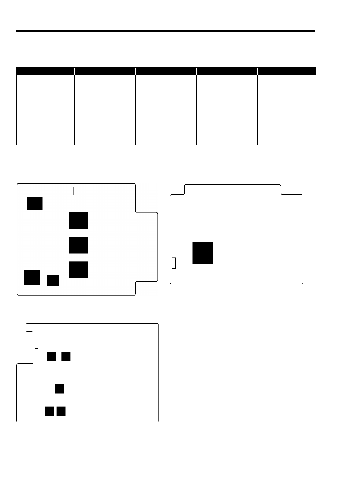
3-2. Layout of parts
AG-MX70 AG-YA70P
Main Board (VEP66448A) Parts Layout SDI Board (VEP83586A) Parts Layout
P1110
IC1330(GMC)
IC1393(ENC)
M16C IC5
SH3 IC233
FS IC711, IC770
ENC IC1393
GMC IC1330
SDI IP502 SDI BOARD
ASPECT IP701
IO IP650
YC LPF IP256, IP306
YC MIX IP651
MAIN BOARD
3D BOARD
IC770(FS)
IC771(FS)
IC233(SH3)
IC5(M16C
AG-VE70P
3D Board (VEP63239A) Parts Layout
P250(Foil Layout
IP306
(YC LPF)
IP256
(YC LPF)
IP701
ASPECT
IP502(SDI
P500
IP650
(IO)
IP651
(YC MIX)
INF-2
3-3. Preparations for updating the internal flash memory microprocessor
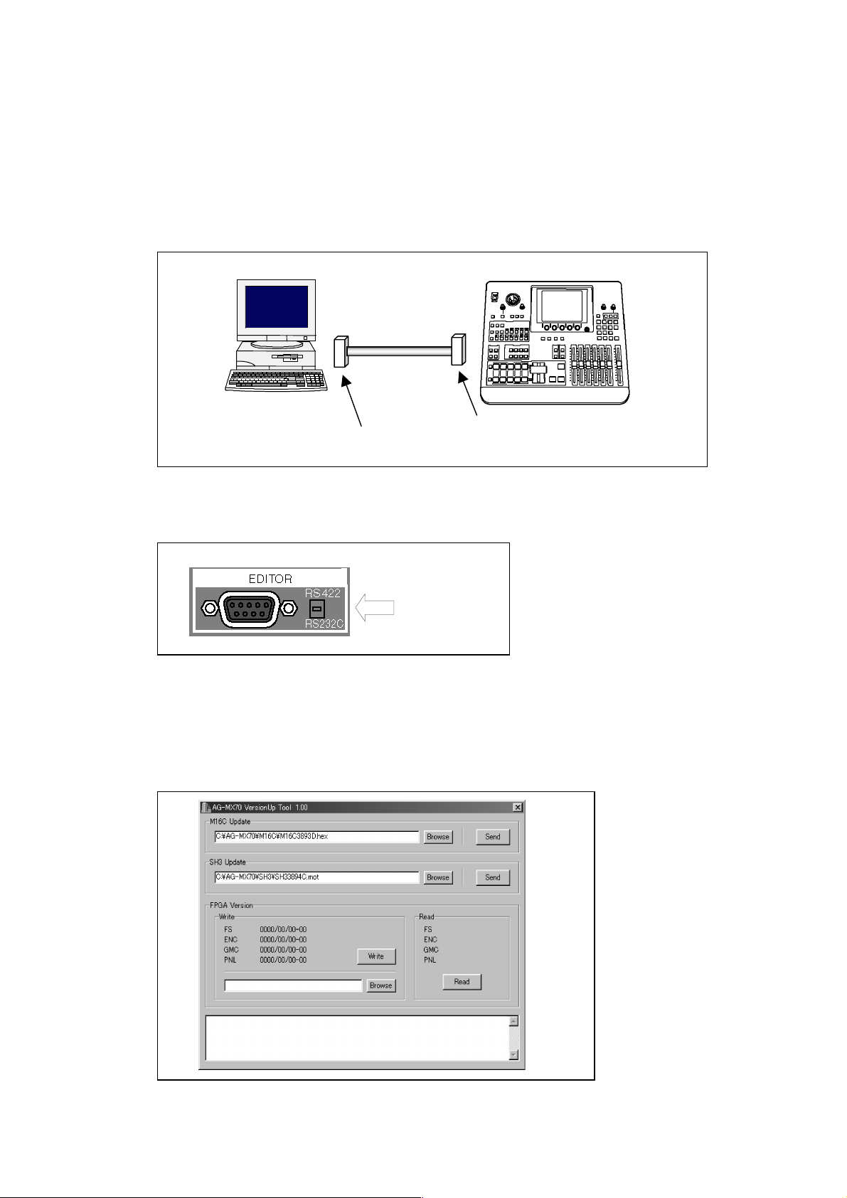
1. Things Needed For Writing
• Writing Software............ VFK1819
• WINDOWS 95/98 Computer
• RS232C cable (9 Pin Straight Cable)
2. Installation Of Writing Software
• Copy the following file into a directory in the computer.
• Program File.................. Version Up Tool. EXE
3. Connection
• With the RS232C cable (9-pin straight cable), connect the AG-MX70 jack panel’s EDITOR
terminal to the computer’s COM port.
D-SUB 9pin
straight cable
PC
Serial port
4. Settings
• Set the switch next to the AG-MX70 jack panel’s EDITOR terminal to RS232C.
Set to RS232C.
EDITOR terminal
AG-MX70
3-4. Steps for updating the internal flash memory microprocessor
1. After completing “3-3. Preparations for updating the internal flash memory microprocessor”, switch on
the computer.
2. Switch on AG-MX70.
3. Start up the writing software. Double-click on the copy of Version Up Tool.EXE.
4. “AG-MX70 Version Up Tool 1.00” opens as follows.
INF-3

5. On AG-MX70, press and hold LUM, AUDIO, EFFECTS ON and 5 and switch the power on. AGMX70 comes on in the flash memory writing mode.
6. Press
+ – on AG-MX70 to change the items on the LCD.
To up date M1C, select [MX70 Flash Write Mode]
To update SH3, select [SH3 Flash Write Mode]
Then press ¿
(the arrow key at the bottom right of the numbered buttons).
7. Wait until the display on the LCD changes from “Now Flash Erase Please Wait” to “Flash Erase Finish
Please Send Data”.
8. In Version Up Tool 1.00, press the “Browse” button in the M16C Update column to update M16C, or
the “Browse” button in SH3 Update to update SH3, and select the writing file.
This is not necessary if the writing file is already in the box.
9. Writing starts when you press the Send button, next to the Browse button.
Confirm that “Now Flash Writing” appears on AG-MX70’s LCD.
If the message doesn’t appear or an error occurs, check the connections and start again.
10. Writing is complete when “Flash Write Complete Please Restart System” appears on AG-MX70’s
LCD.
11. Switch AG-MX70 off then on again and enter the SETUP menu. The version information appears by
pressing and holding
SHIFT and 8 for 3 seconds. Confirm that the version has changed.
INF-4
3-5. Updating the PLD (Altera)
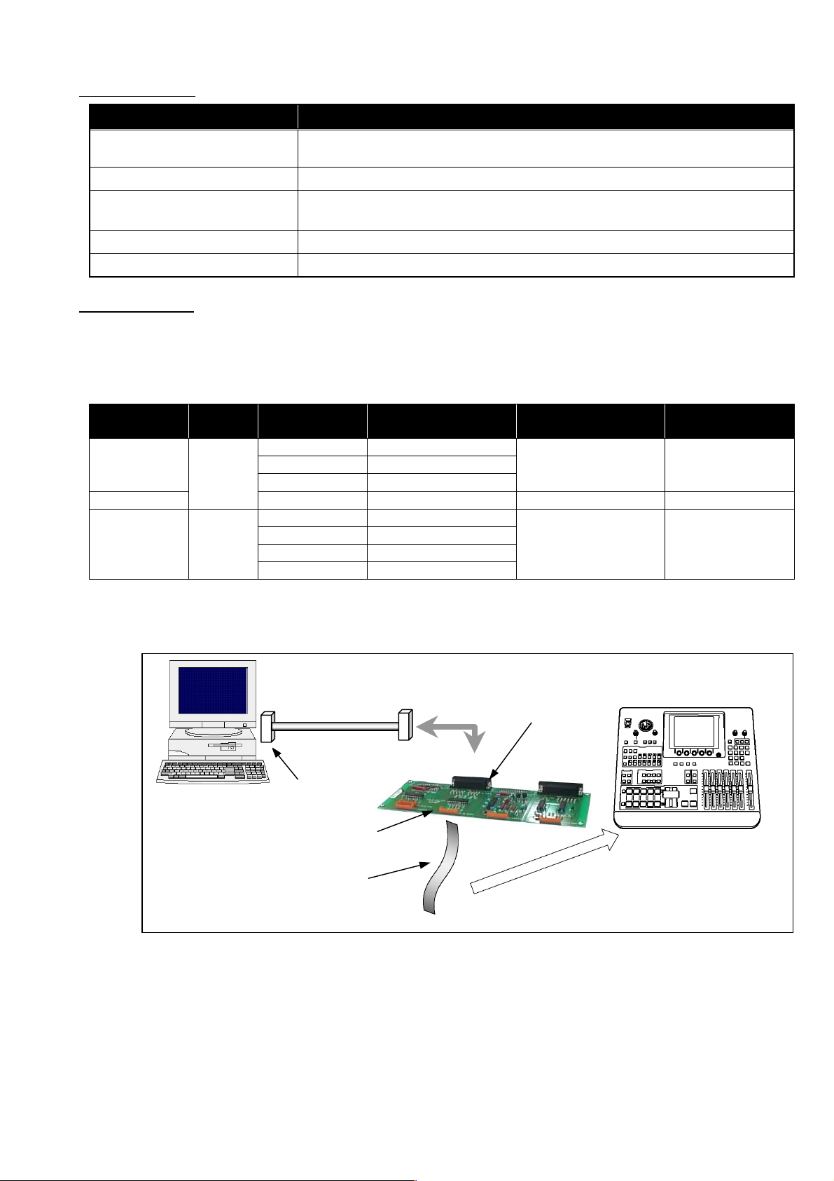
A. Preparation
EQUIPMENT REMARKS
CPLD Writer
25-pin-25-pin Cable Straight (male-female), within 1 meter
Writing Software
Version Updater Tdf format or pof format file (Included in VSI**** file)
Computer Windows 95 or 98 installed
B. Connection
1. Connect the computer and the CN201 connector (for Altera) on the CPLD writer (VFK1590) with the 25pin-25-pin cable.
2. Connect the writing connectors on the FPGA and PGA you are updating to the P201 connector on the
CPLD writer with the cable included with the CPLD writer (VFK1590).
VFK1590
VFK1590P2 (Cable: included with VFK1590)
MAX+plus II Software: WWW.altera.com./pub/software/asap2.exe
Download from the URL and save in a directory
MODEL NO. TYPE NAME REFERENCE NO.
WRITING
CONNECTOR NO.
BOARD NAME
FS IC711, IC770
AG-YA70P
FPGA
ENC IC1393AG-MX70
GMC IC1330
SDI IP502 P500 SDI BOARD
P1110 MAIN BOARD
ASPECT IP701
AG-VE70P PLD
IO IP650
YC LPF IP256, IP306
P250 3D BOARD
YC MIX IP651
3. Start up the unit and the computer in Windows mode.
4. Copy all the VVVSI**** files including “*.jcf” to a floppy6 disc. Insert the floppy disc into your computer’s
disc drive.
Computer
D-SUB 25 pins
Cable
CPLD Writer
VFK1590
To Print Port
Connector
CN201
Connector P201
Cable
VFK1590P2
AG-MX70
Writing connectors (Refer to above table)
INF-5
C. Starting the writing software and steps for updating
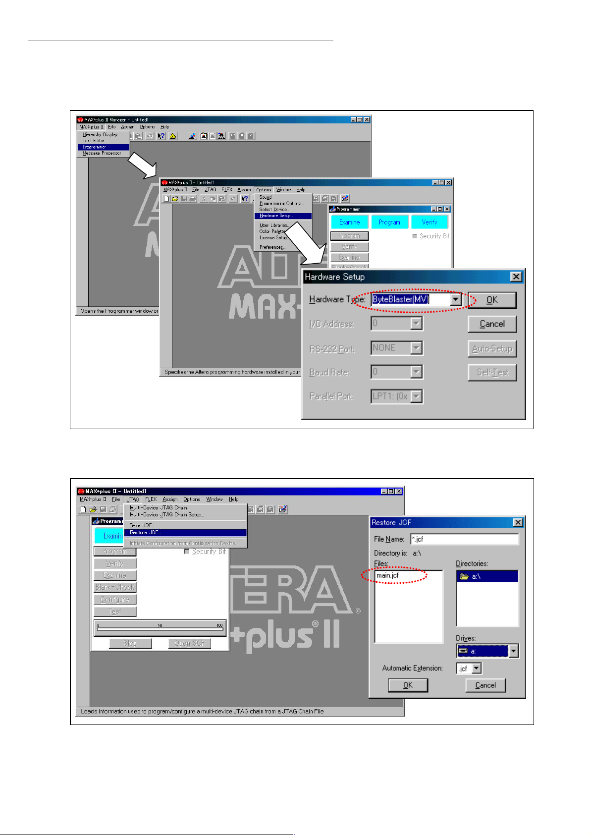
1. From the Windows START menu, select Program MAX+plus II*.*programmer only.
2. In the main window, from the MAX+plus II tab select Programmer.
3. In the main window after displaying the Programmer screen, from the Option tab select Hardware Setup.
4. In the Hardware Setup window, set Hardware Type to ByteBlaster (MV).
5. In the main window, from the JTAG tab select Restore JCF…
6. In the Restore JCF dialog, select the floppy disc drive [A:]. Next select “jcf format file (****.jcf) and click
OK.
INF-6
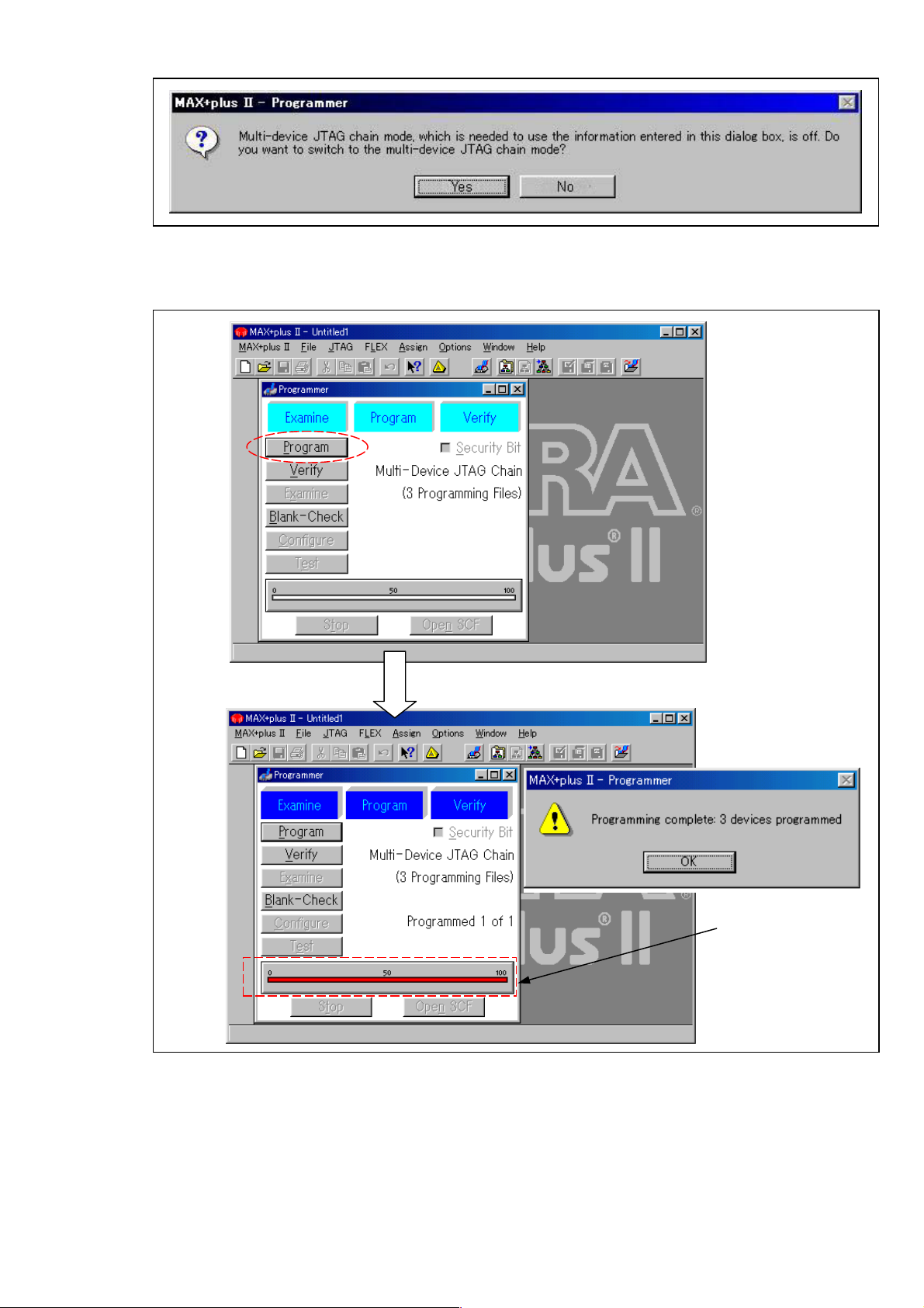
7. If the following dialog appears, click Yes to proceed to the next step.
8. In the Programmer dialog, click Program.
9. PLD writing is complete when the progress bar at the bottom of the dialog reaches 100. The message
“Programming complete” appears, so click OK.
Progress bar
* MAX+plus is a registered trademark of Altera Corporation in the United States and other countries.
* Windows 95 and Windows 98 are registered trademarks of Microsoft Corporation in the United States and other countries.
INF-7
4. The way of attaching an option board
4-1. Installation of the AG-YA70P
The AG-YA70P is an interface board that enables the AG-MX70 to be connected to a serial digital interface (SDI).
Follow the procedure below to install it.
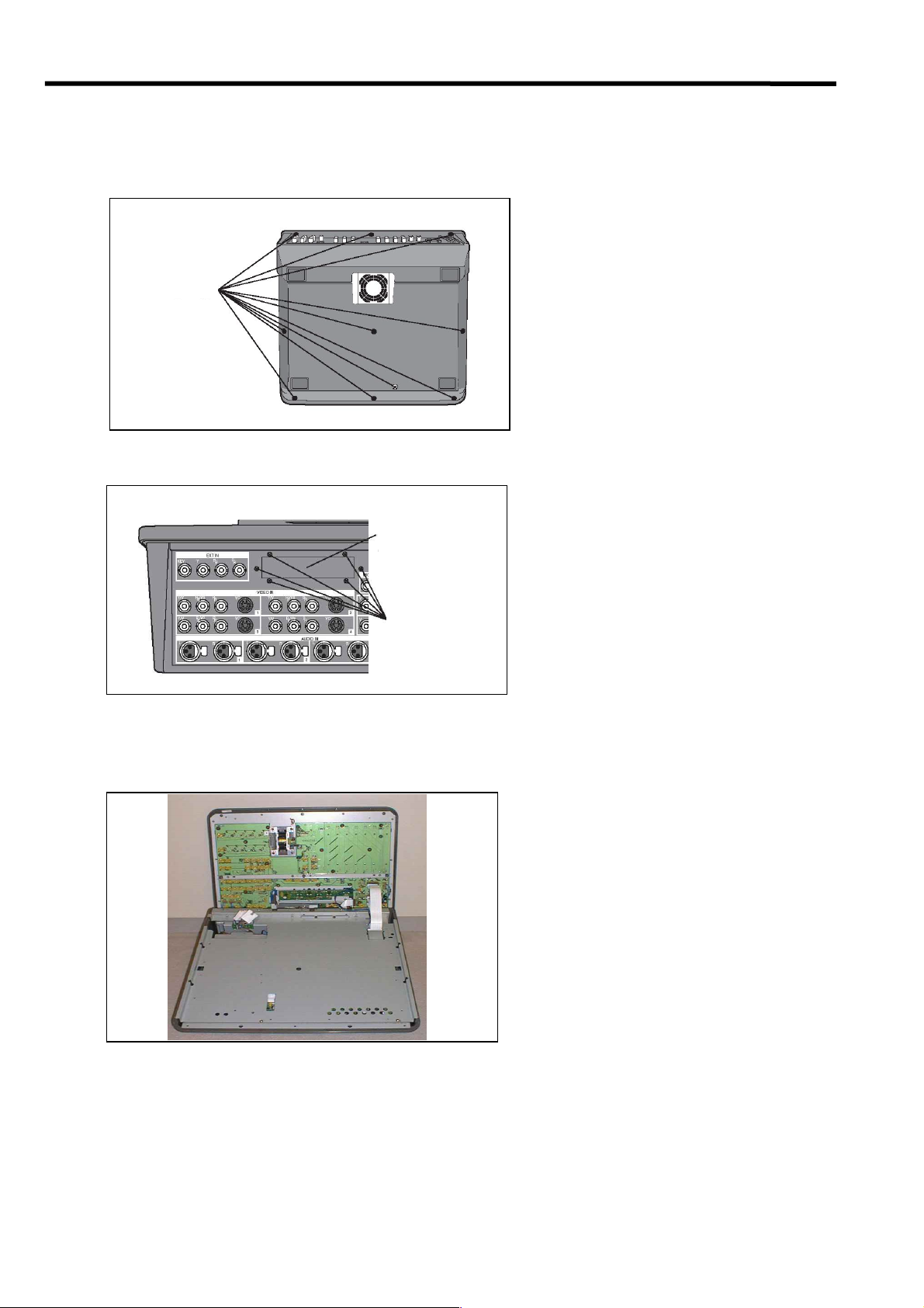
1. Turn off the power of the AG-MX70 and remove the ten screws from the bottom panel.
Screws (10 pcs)
2. Remove the six screws from the rear panel, then remove the blank panel.
Blank panel
Screws (6 pcs)
3. Open the top unit, including the LCD, from the front, then release the bands securing the flexible cable and
blue cable of the unit.
4. Fix the unit perfectly upright so it does not topple. When removing the casing, ensure the flexible and other
cables do not become detached.
INF-8

5. Remove the twenty screws from the shield casing, then remove the casing itself.
Screws
(20 pcs)
6. Remove the two hexagonal screws for anchoring the AG-YA70P to the motherboard.
Fixing screws
for AG-YA70P
Fixing screws
for AG-VE70P
7. Insert the AG-YA70P board. (Refer to the figure at left.)
INF-9
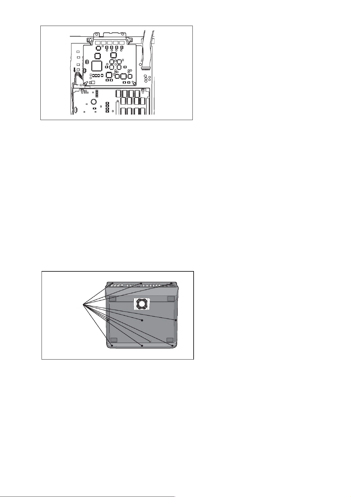
8. Insert the cable from the AG-YA70P into the connector on the motherboard. (Refer to the figure at left.)
9. Secure the two screws which were removed in step 6.
10. Secure the shield casing and the twenty screws which were removed in step 5.
11. Re-attachthebandsremovedinstep3.andclosethetopunit.
12.Securethesixscrewswhichwereremovedinstep2.
13.Securethetenscrewswhichwereremovedinstep1.
4-2. Installation of the AG-VE70P
The AG-VE70P is a 3D effect board that enables the 3D patterns, etc. of the AG-MX70 to be used.
Follow the procedure below to install it.
1. Turn off the power of the AG-MX70 and remove the ten screws from the bottom panel.
Screws (10 pcs)
INF-10
2. Open the unit in the top part including the LCD out toward the front, then release the bands securing the
flexible cable and blue cable of the unit.
3. Fix the unit perfectly upright so it does not topple.
When removing the casing, ensure the flexible and other c ables do not become detached.
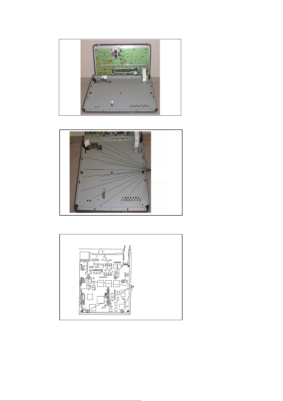
4. Remove the twenty screws from the shield casing, then remove the casing itself.
Screws
(20 pcs)
5. Remove the five hexagonal screws for anchoring the AG-VE70P to the motherboard.
Fixing screws
for AG-YA70P
Fixing screws
for AG-VE70P
INF-11
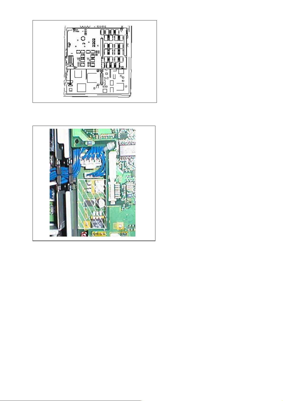
6. Insert the AG-VE70P board. (Refer to the figure at right.)
7. Insert the cable from the AG-VE70P into the connector on the motherboard. (Refer to the figure at left.)
Route the cables while carefully ensuring that they do not make contact with the transition lever unit.
8. Securethefivescrewswhichwereremovedinstep5.
9. Securetheshieldcasingandthetwentyscrewswhichwereremovedinstep4.
10. Re-attach the bands removed in step 2. and close the top unit.
11.Securethetenscrewswhichwereremovedinstep1.
INF-12

DISASSEMBLY PROCEDURES
CO
S
NTENT
1. Removal the Top Case ...................................................................................... DIS-1
2. Removing the LCD Panel .................................................................................. DIS-1
3. Removal the Top Case Fan Motor.................................................................... DIS-2
4. Removal the Bottom Case Fan Motor.............................................................. DIS-2
5. Removal the Power Unit.................................................................................... DIS-2
6. Removal the Power Unit's Fan Motor .............................................................. DIS-2
7. Removal the Jack Unit ...................................................................................... DIS-3

1. Removal the Top Case
1. Unscrew the 9 screws (A) and the screw (B) in the
illustration.
SCREW (A)
SCREW (B)
BOTTOM
CASE
TOP CASE
2. Open the Top Case and disconnect P15 connector
on the Panel P.C.Board and the connector on AC
SW.
3. Unlock P5, P6, and P8, disconnect the flexible cable
and remove the Top Case.
SCREW (A)
SCREW (C)
3. Disconnect connectors P1102, P1103, and P1104
and remove the Inverter Angle.
SCREW (A)
SCREW (B)
INVERTER ANGLE
SCREW (C)
P1102
PANEL P.C.BOARD
P5
P6
P8
AC SW
CONNECTOR
P15
2. Removing the LCD Panel
1. Remove the Top Case.
2. Unscrew the 6 screws (A), the 3 screws (B), and the
2 screws (C) in the illustration.
P1104
4. Unscrew the 4 screws (D) and remove the LCD
Panel.
SCREW (D)
SCREW (D)
P1103
LCD PANEL
DIS - 1
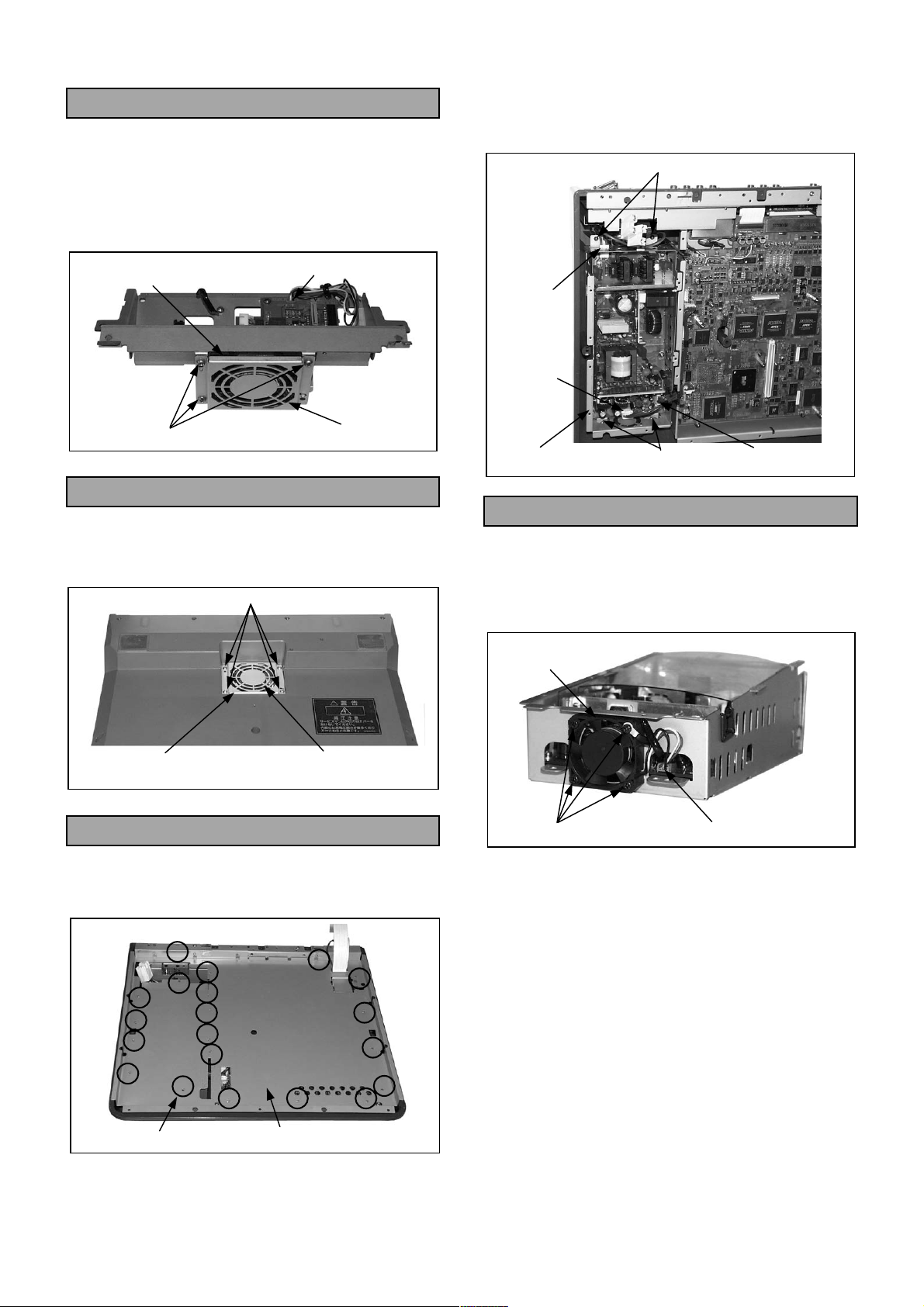
3. Removal the Top Case Fan Motor
1. Remove the Top Case.
2. Remove the Inverter Angle. (See "Removal the
LCD Panel")
3. Unscrew the 3 screws and remove the Fan Cover.
4. Disconnect connector P1105 and remove the Top
Case Fan Motor.
3. Unscrew the 4 screws (B).
4. Disconnect P1001, P1103 and P1104 and remove
the Power Unit.
SCREW (B)
TOP CASE FAN MOTOR
SCREW
P1105
FAN COVER
4. Removal the Bottom Case Fan Motor
1. Unscrew the 4 screws and remove the Fan Cover.
2. Remove the Bottom Case Fan Motor and
disconnect the connectors.
SCREW
P1001
P1104
POWER UNIT
SCREW (B)
P1103
6. Removal the Power Unit's Fan Motor
1. Remove the Power Unit.
2. Unscrew the 4 screws.
3. Disconnect connector P1106 and remove the
Power Unit's Fan Motor.
POWER UNIT’S
FAN MOTOR
BOTTOM CASE FAN MOTORFAN COVER
5. Removal the Power Unit
1. Remove the Top Case.
2. Unscrew the 20 screws (A) and remove the Main
Case Cover.
SCREW (A)
MAIN CASE COVER
SCREW P1106
DIS - 2
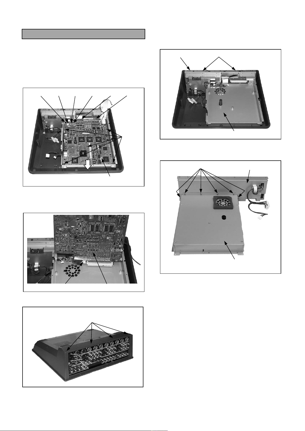
7. Removal the Jack Unit
1. Remove the Power Unit.
7. Unscrew the 2 screws (C) and remove the Jack
Unit along with the Main Case.
2. Unscrew the 5 screws (A).
3. Disconnect connectors P361, P366, P1111, and
P1112, unlock connector P365, and disconnect the
flexible cable.
4. Slide the Main P.C.Board in the direction indicated
by the arrow and disconnect connector P360.
P361 P366 P1112 P1111 P365 P360
SCREW
(A)
MAIN P.C.BORAD
5. Lift the Main P.C.Board as shown in the illustration,
disconnect connector P364, and remove the Main
P.C.Board.
JACK UNIT
8. Unscrew the 6 screws (D) and separate the Jack
Unit from the Main Case.
SCREW (D)
SCREW (C)
MAIN CASE
JACK UNIT
P364
6. Unscrew the 4 screws (B).
SCREW (B)
MAIN CASE
MAIN P.C.BORAD
DIS - 3

ELECTRICAL ADJUSTMENTS
CONTENTS
1. MAIN .......................................................................................................................EAD-1
1-1. PLL Free run frequency adjustment ...................................................................................... EAD-1
1-2. Adjustment of Y output gain of component signals ............................................................... EAD-1
1-3. Adjustment of PB output gain of component signals............................................................. EAD-1
1-4. Adjustment of PR output gain of component signals ............................................................ EAD-1
1-5. Adjustment of output gain of composite signals .................................................................... EAD-2
1-6. Adjust output gain of PVW (preview)..................................................................................... EAD-2
1-7. Adjustment of output gain of Y/C (S terminal) signals........................................................... EAD-2
1-8. Adjustment of output gain of ADV-REF signals..................................................................... EAD-2
1-9. Preparation before starting the adjustment menu ................................................................. EAD-3
1-10. Starting the adjustment menu................................................................................................ EAD-3
1-11. SCH adjustment .................................................................................................................... EAD-3
1-12. Adjust component Y input signal gain of the A bus............................................................... EAD-4
1-13. Adjust component PB input signal gain of the A bus ............................................................ EAD-4
1-14. Adjust component PR input signal gain of the A bus ............................................................ EAD-4
1-15. Adjust component Y input signal gain of the B bus............................................................... EAD-5
1-16. Adjust component PB input signal gain of the B bus ............................................................ EAD-5
1-17. Adjust component PR input signal gain of the B bus ............................................................ EAD-5
1-18. Adjustment of EXT input signal gain ..................................................................................... EAD-6
1-19. Adjustment of EXT input signal PB offset.............................................................................. EAD-6
1-20. Adjustment of EXT input signal PR offset ............................................................................. EAD-6
1-21. Adjustment of EXT input signal PB gain................................................................................ EAD-7
1-22. Adjustment of EXT input signal PR gain ............................................................................... EAD-7
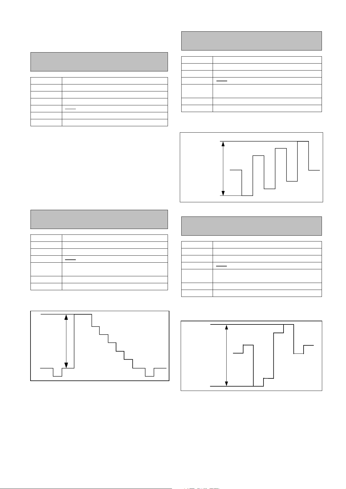
1. MAIN
1-3. Adjustment of PB output gain
of component signals
1-1. PLL Free Run Frequency
Adjustment
BOARD MAIN BOARD
TP TP1393
ADJ. VR1490
INPUT No Input to EXT-Y, EXT-Key, and G/L
MODE
M.EQ Frequency Counter
SPEC. Within 27, 000, 000 MHz ±30 Hz
1. Measure TP1393 with the frequency counter and
adjust VR1490 so it meets the above
specifications.
Note:
If there are input signals to EXT-Y, EXT-Key, and
G/L, PLL will respond to the signals so there will be no
change even if you adjust the frequency with VR1490.
1-2. Adjustment of Y output gain
of component signals
BOARD MAIN BOARD
TP VIDEO OUT,Y1 or Y2
ADJ. VR1524 (Y)
INPUT
MODE
M.EQ Oscilloscope
SPEC. Y level: within 700±14 mV
1. Adjust VR1524 (Y) so the Y1 or Y2 level of VIDEO
OUT becomes 700±14 mV.
Cross point: A bus, B bus = INT
LCD menu: Int Video = colorbar
BOARD MAIN BOARD
TP VIDEO OUT, PB1 or PB2
ADJ. VR1522 (PB)
INPUT
MODE
M.EQ Oscilloscope
SPEC. PB level: within 525±10 mV
1. Adjust VR1522 (PB) so the PB1 or PB2 level of
VIDEO OUT becomes 525±10 mV.
PB LEVEL
Cross point: A bus, B bus = INT
LCD menu: Int Video = colorbar
1-4. Adjustment of PR output gain
of component signals
BOARD MAIN BOARD
TP VIDEO OUT,PR1 or PR2
ADJ. VR1520 (PR)
INPUT
MODE
M.EQ Oscilloscope
SPEC. PR level: within 525±10 mV
1. Adjust VR1520 (PR) so the PR1 or PR2 level of
VIDEO OUT becomes 525±10 mV.
Cross point: A bus, B bus = INT
LCD menu: Int Video = colorbar
Y LEVEL
EAD-1
PR LEVEL
PR LEVEL
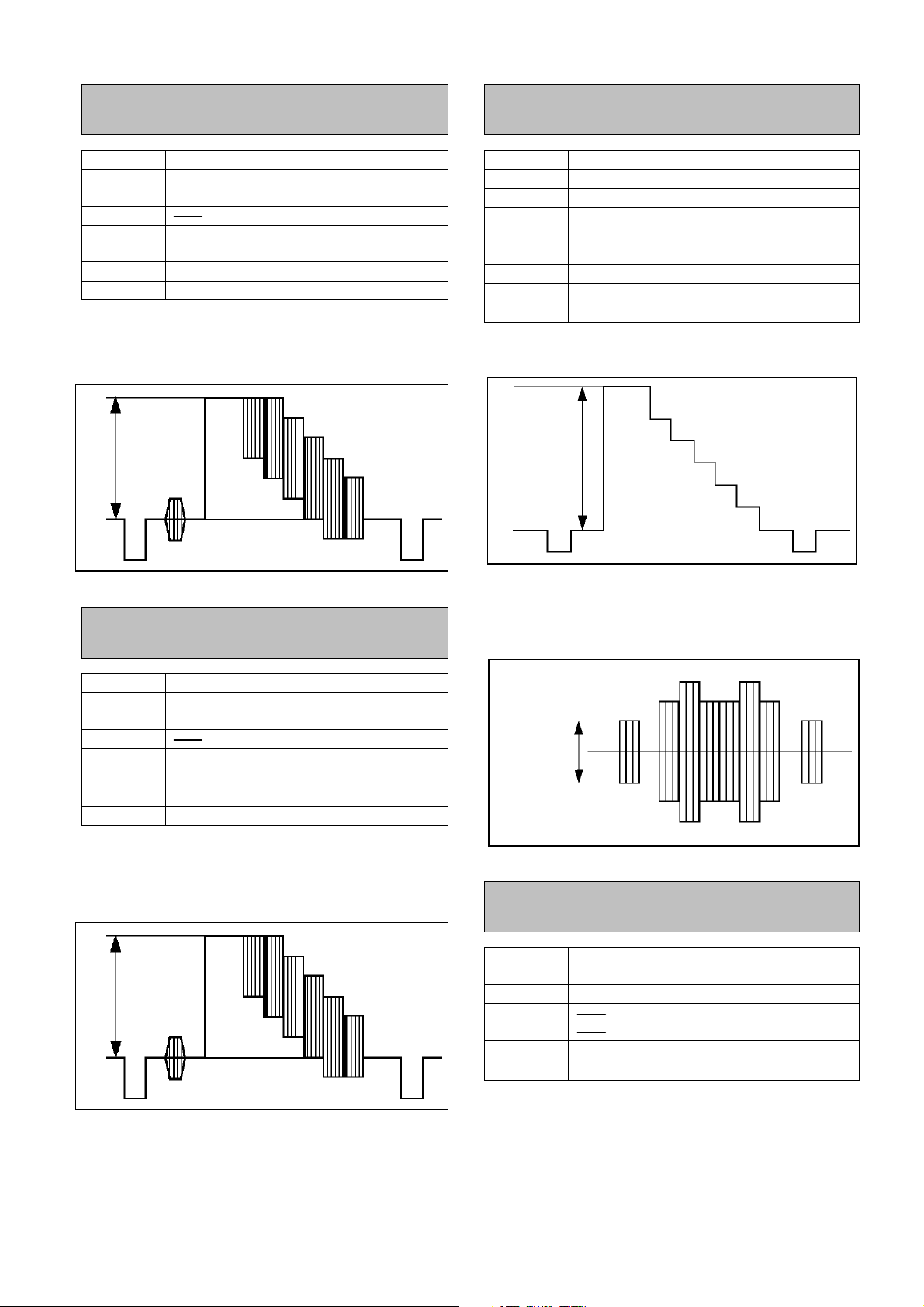
1-5. Adjustment of output gain of
composite signals
1-7. Adjustment of output gain of
Y/C (S terminal) signals
BOARD MAIN BOARD
TP VIDEO OUT,V1 or V2
ADJ. VR1525 (VIDEO)
INPUT
MODE
M.EQ
SPEC. A = within 700±14mV
1. Adjust VR1525 (VIDEO) so the composite signal
output level of V1 or V2 level of VIDEO OUT
becomes 700±14mV.
A
Cross point: A bus, B bus = INT
LCD menu: Int Video = color bar
Oscilloscope
BOARD MAIN BOARD
TP
ADJ. VR1561 (YCT), VR1523 (YCC)
INPUT
MODE
M.EQ
SPEC.
1. Adjust VR1561 (YCT) so the Y level of YC1 or
YC2 of VIDEO OUT becomes 700 ±14 mV.
Y LEVEL
2. 2. Adjust VR1523 (YCC) so the C level of
VIDEO OUT,YC1 or YC2
Cross point: A bus, B bus = INT
LCD menu: Int Video = color bar
Oscilloscope
Y level: within 700 ±14 mV
C level: within 300 ± 6 mV
1-6. Adjust output gain of PVW
(preview)
BOARD MAIN BOARD
TP PREVIEW
ADJ. VR1521 (AUX)
INPUT
MODE
M.EQ
SPEC.
1. Adjust VR1521 (AUX) so the composite signal
output level PVW (preview) becomes
700±14mV.
A
Cross point: A bus, B bus = INT
LCD menu: Int Video = color bar
Oscilloscope
A = within 700±14mV
YC1 or YC2 of VIDEO OUT becomes 300 ± 6
mV.
C LEVEL
1-8. Adjustment of output gain of
ADV-REF signals
BOARD MAIN BOARD
TP ADV-REF
ADJ. VR1560 (REF)
INPUT
MODE
M.EQ
SPEC.
Oscilloscope
SYNC level: within 300 ±6 mV
EAD-2
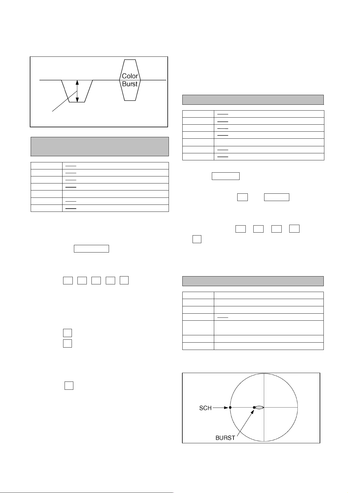
1. Adjust VR1560 (REF) so the SYNC level of
3. Confirm the settings: You do not have to do this
ADV-REF becomes 300 ±6 mV
SYNC LEVEL
1-9. Preparation before starting
the adjustment menu
BOARD
TP
ADJ.
INPUT
MODE
M.EQ
SPEC.
Do the following before starting the adjustment
menu.
1. Make the pattern No.=0002.
a Press the PATTERN key (at the top left of
the 10 key block) to light it.
You do not have to press it if it is already lit.
Adjustment menu mode
if you have not changed the settings from the
default.
a In the LCD menu: Check that SETUP/Gen.
Lock/Refin = G/L. If it is not, change it so it is.
1-10. Starting the adjustment menu
BOARD
TP
ADJ.
INPUT
MODE
M.EQ
SPEC.
Start the adjustment menu.
1. Press SETUP so the SET UP screen
appears on the LCD.
2. Press and hold 9 and SHIFT (in the 10-
key block) for 3 seconds.
The adjustment menu appears on the LCD.
3. In order, press 0 , 2 , 6 , - and
¿ .
The unit is now ready to accept commands
from the rotary encoder.
Adjustment menu mode
b Press 0 ,0,0,2, ¿ in order.
The pattern No. is set to 0002.
2. Set SOURCE-1 to analog component input.
a In the LCD menu: Select the SETUP/Audio
Video/InputSetup line.
b Press ¿ once. “OK?” appears.
c Press ¿ once again.
The AudioVideoSetup screen appears.
d Change “Video” in the top line (“V S-1”) to “Y
Pb Pr” with the rotary encoder.
e Press ¿ to exit the Audio Video Setup
screen.
1-11. SCH adjustment
BOARD MAIN BOARD
TP
ADJ.
INPUT
MODE
M.EQ
SPEC.
1. Adjust the SCH in the adjustment menu so the
SCH of VIDEO OUT V1 or V2 becomes 0±2º.
VIDEO OUT V1 or V2
Adjustment menu/ rotary encoder
Adjustment menu, A bus, B bus =
SOURCE-1
SCH meter
SCH: within 0±2º
EAD-3
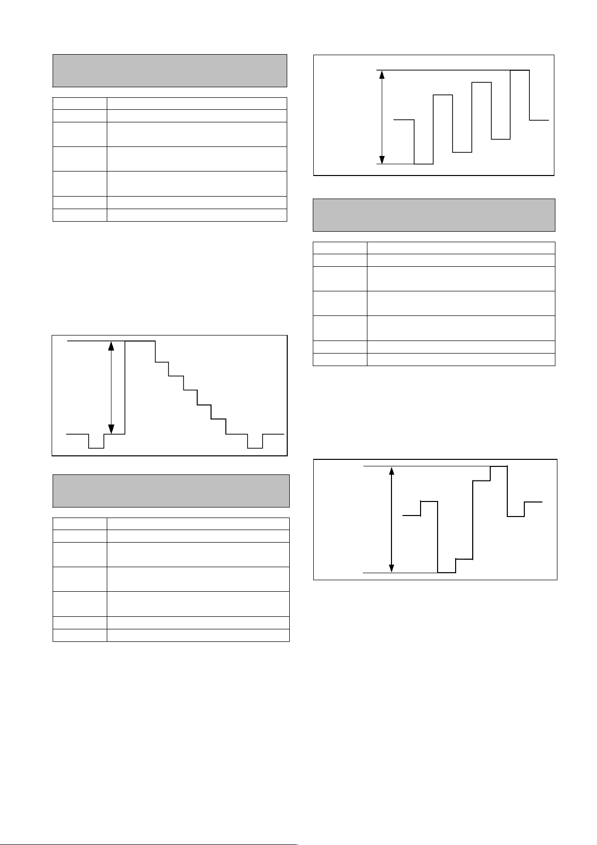
1-12. Adjust component Y input
signal gain of the A bus
BOARD MAIN BOARD
TP
ADJ.
INPUT
MODE
M.EQ
SPEC.
1. Use the rotary encoder to select “A-bus” in the
adjustment menu.
2. Use the rotary encoder to adjust “Y-Gain” so
the level of VIDEO OUT Y1 or Y2 becomes
700±
14mV.
Y LEVEL
VIDEO OUT Y1 or Y2
Adjustment menu/rotary encoder (YGain)
Analog component signal (75% color
bar, 0 setup)
A bus, B bus = SOURCE-1
Take lever to A bus side
Oscilloscope
Y level: within 700±14mV
PB LEVEL
1-14. Adjust component PR input
signal gain of the A bus
BOARD MAIN BOARD
TP
ADJ.
INPUT
MODE
M.EQ
SPEC.
1. Use the rotary encoder to select “A-bus” in the
adjustment menu.
VIDEO OUT PR 1 or PR 2
Adjustment menu/rotary encoder (Pr Gain)
Analog component signal (75% color
bar, 0 setup)
A bus, B bus = SOURCE-1
Take lever to A bus side
Oscilloscope
PR level: within 525±10mV
1-13. Adjust component PB input
signal gain of the A bus
BOARD MAIN BOARD
TP
ADJ.
INPUT
MODE
M.EQ
SPEC.
1. Use the rotary encoder to select “A-bus” in the
adjustment menu.
2. Use the rotary encoder to adjust “PB -Gain” so
VIDEO OUT PB 1 or PB 2
Adjustment menu/rotary encoder (Pb
-Gain)
Analog component signal (75% color
bar, 0 setup)
A bus, B bus = SOURCE-1
Take lever to A bus side
Oscilloscope
PB level: within 525±10mV
2. Use the rotary encoder to adjust “Pr -Gain” so
the level of VIDEO OUT PR 1 or PR 2 becomes
525±10mV.
PR LEVEL
the level of VIDEO OUT PB 1 or PB 2 becomes
525±10mV.
EAD-4
 Loading...