

ON Semiconductor 2N6107, 2N6109, 2N6111, 2N6288, 2N6292 Service Manual
PNP - 2N6107, 2N6109,
2N6111; NPN - 2N6288,
2N6292
2N6109 and 2N6292 are Preferred Devices
Complementary Silicon
Plastic Power Transistors
These devices are designed for use in general-purpose amplifier and
switching applications.
Features
•DC Current Gain Specified to 7.0 Amperes
hFE= 30-150 @ I
= 3.0 Adc - 2N6111, 2N6288
= 2.3 (Min) @ IC = 7.0 Adc - All Devices
C
•Collector-Emitter Sustaining Voltage -
V
CEO(sus)
= 30 Vdc (Min) - 2N6111, 2N6288
= 50 Vdc (Min) - 2N6109
= 70 Vdc (Min) - 2N6107, 2N6292
•High Current Gain - Bandwidth Product
fT= 4.0 MHz (Min) @ IC = 500 mAdc - 2N6288, 90, 92
= 10 MHz (Min) @ IC = 500 mAdc - 2N6107, 09, 11
•TO-220AB Compact Package
•Pb-Free Packages are Available*
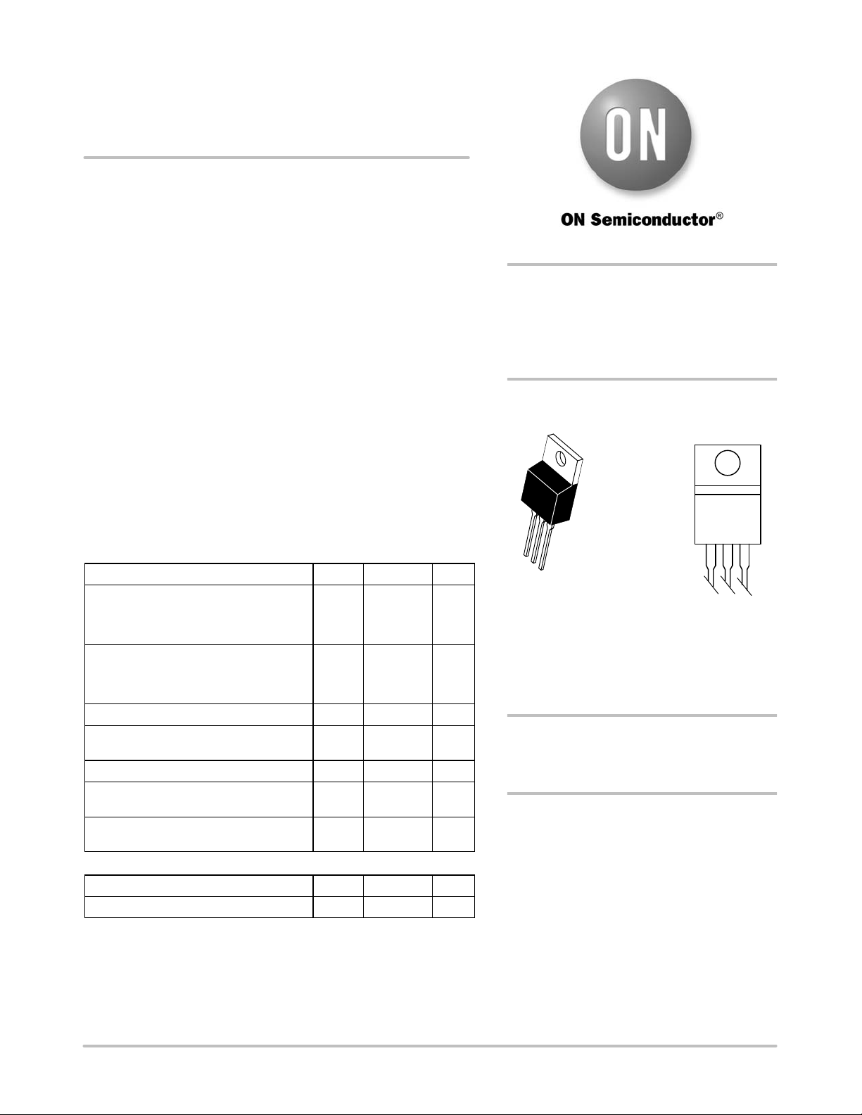
MAXIMUM RATINGS (Note 1)
Rating Symbol Value Unit
Collector-Emitter Voltage
2N6111, 2N6288
2N6109
2N6107, 2N6292
Collector-Base Voltage
2N6111, 2N6288
2N6109
2N6107, 2N6292
Emitter-Base Voltage V
Collector Current - Continuous
- Peak
Base Current I
Total Power Dissipation @ TC = 25_C
Derate above 25_C
Operating and Storage Junction
Temperature Range
V
CEO
V
I
P
TJ, T
CB
EB
C
B
D
-65 to +150 °C
stg
30
50
70
40
60
80
5.0 Vdc
7.0
10
3.0 Adc
40
0.32
Vdc
Vdc
Adc
W
W/°C
http://onsemi.com
7 AMPERE
POWER TRANSISTORS
COMPLEMENTARY SILICON
30 - 50 - 70 VOLTS, 40 WATTS
MARKING
DIAGRAM
4
TO-220AB
CASE 221A
STYLE 1
1
2
3
2N6xxx = Specific Device Code
xxx = See Table on Page 4
G = Pb-Free Package
A = Assembly Location
Y = Year
WW = Work Week
ORDERING INFORMATION
See detailed ordering, marking, and shipping information in
the package dimensions section on page 4 of this data sheet.
Preferred devices are recommended choices for future use
and best overall value.
2N6xxxG
AYWW
THERMAL CHARACTERISTICS
Characteristics Symbol Max Unit
Thermal Resistance, Junction-to-Case
Stresses exceeding Maximum Ratings may damage the device. Maximum
Ratings are stress ratings only. Functional operation above the Recommended
Operating Conditions is not implied. Extended exposure to stresses above the
Recommended Operating Conditions may affect device reliability.
1. Indicates JEDEC Registered Data.
*For additional information on our Pb-Free strategy and soldering details, please
download the ON Semiconductor Soldering and Mounting Techniques
Reference Manual, SOLDERRM/D.
© Semiconductor Components Industries, LLC, 2007
November, 2007 - Rev. 8
R
q
JC
3.125
_C/W
1 Publication Order Number:
2N6107/D
PNP - 2N6107, 2N6109, 2N6111; NPN - 2N6288, 2N6292
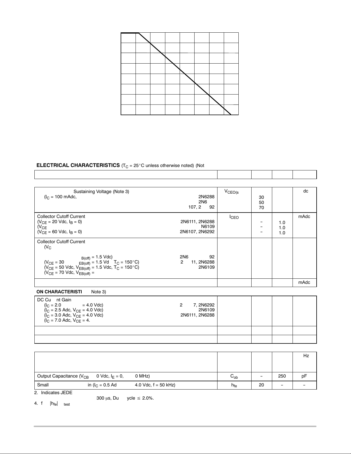
40
30
20
10
, POWER DISSIPATION (WATTS)
D
P
0
0 20 40 60 80 100 120 160
TC, CASE TEMPERATURE (°C)
Figure 1. Power Derating
140
ELECTRICAL CHARACTERISTICS (T
= 25_C unless otherwise noted) (Note 2)
C
Characteristic
OFF CHARACTERISTICS
Collector-Emitter Sustaining Voltage (Note 3)
(IC = 100 mAdc, IB = 0) 2N6111, 2N6288
2N6109
2N6107, 2N6292
Collector Cutoff Current
(VCE = 20 Vdc, IB = 0) 2N6111, 2N6288
(VCE = 40 Vdc, IB = 0) 2N6109
(VCE = 60 Vdc, IB = 0) 2N6107, 2N6292
Collector Cutoff Current
(VCE = 40 Vdc, V
(VCE = 60 Vdc, V
(VCE = 80 Vdc, V
(VCE = 30 Vdc, V
(VCE = 50 Vdc, V
(VCE = 70 Vdc, V
= 1.5 Vdc) 2N6111, 2N6288
EB(off)
= 1.5 Vdc) 2N6109
EB(off)
= 1.5 Vdc) 2N6107, 2N6292
EB(off)
= 1.5 Vdc, TC = 150_C) 2N6111, 2N6288
EB(off)
= 1.5 Vdc, TC = 150_C) 2N6109
EB(off)
= 1.5 Vdc, TC = 150_C) 2N6107, 2N6292
EB(off)
Emitter Cutoff Current (VBE = 5.0 Vdc, IC = 0)
ON CHARACTERISTICS (Note 3)
DC Current Gain
(IC = 2.0 Adc, VCE = 4.0 Vdc) 2N6107, 2N6292
(IC = 2.5 Adc, VCE = 4.0 Vdc) 2N6109
(IC = 3.0 Adc, VCE = 4.0 Vdc) 2N6111, 2N6288
(IC = 7.0 Adc, VCE = 4.0 Vdc) All Devices
Collector-Emitter Saturation Voltage (IC = 7.0 Adc, IB = 3.0 Adc)
Base-Emitter On Voltage (IC = 7.0 Adc, VCE = 4.0 Vdc)
DYNAMIC CHARACTERISTICS
Current Gain — Bandwidth Product (Note 4)
(IC = 500 mAdc, VCE = 4.0 Vdc, f
= 1.0 MHz) 2N6288, 92
test
2N6107, 09, 11
Output Capacitance (VCB = 10 Vdc, IE = 0, f = 1.0 MHz)
Small-Signal Current Gain (IC = 0.5 Adc, VCE = 4.0 Vdc, f = 50 kHz)
2. Indicates JEDEC Registered Data.
3. Pulse Test: Pulse Width v 300 ms, Duty Cycle v 2.0%.
4. fT = |hfe| • f
test
Symbol
V
CEO(sus)
I
CEO
I
CEX
I
EBO
h
FE
V
CE(sat)
V
BE(on)
f
T
C
ob
h
fe
Min
30
50
70
-
-
-
-
-
-
-
-
-
-
30
30
30
2.3
-
-
4.0
10
-
20
Max
-
-
-
1.0
1.0
1.0
100
100
100
2.0
2.0
2.0
1.0
150
150
150
-
3.5
3.0
-
-
250
-
Unit
Vdc
mAdc
mAdc
mAdc
mAdc
-
Vdc
Vdc
MHz
pF
-
http://onsemi.com
2
 Loading...