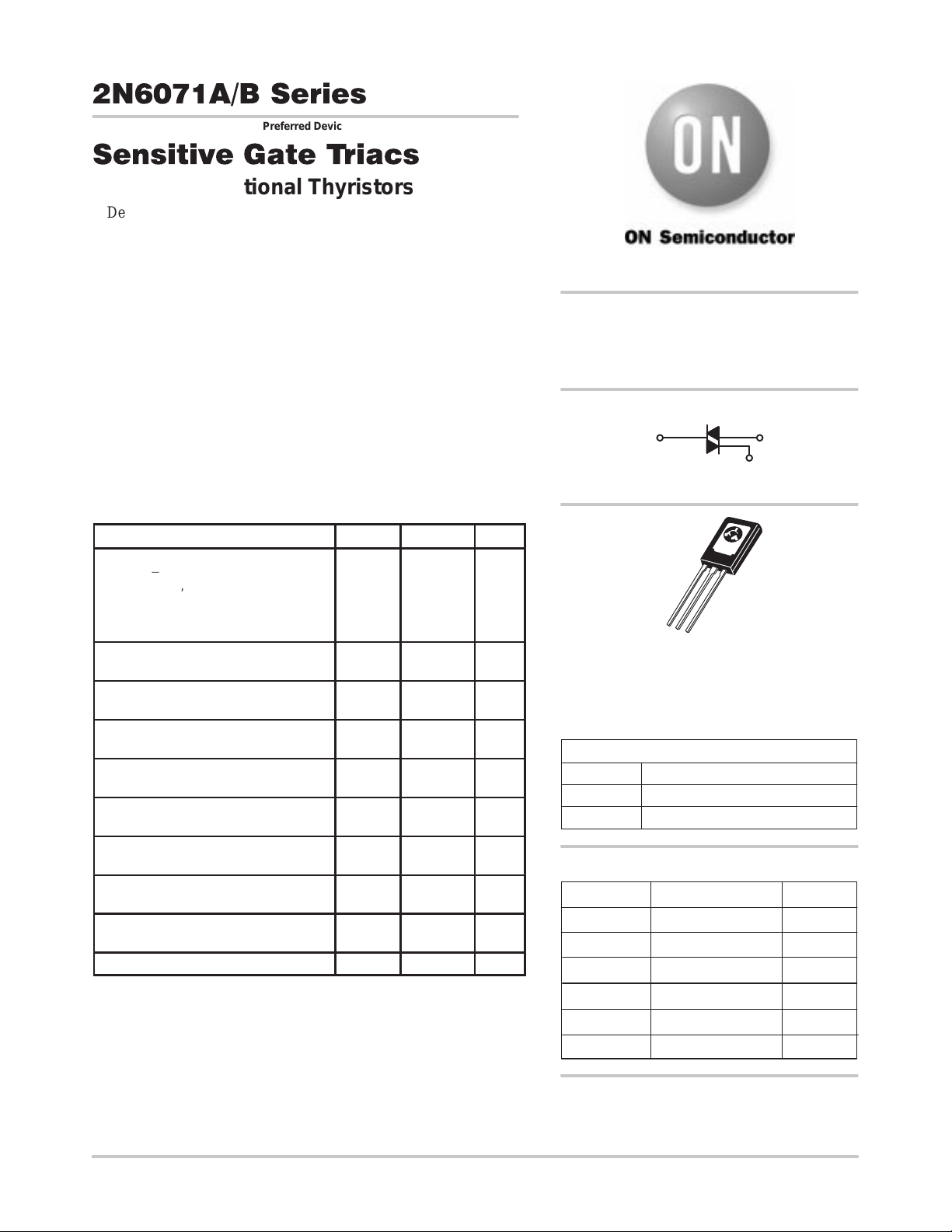
2N6071A/B Series
Preferred Device
Sensitive Gate Triacs
Silicon Bidirectional Thyristors
Designed primarily for full-wave ac control applications, such as
light dimmers, motor controls, heating controls and power supplies; or
wherever full-wave silicon gate controlled solid-state devices are
needed. Triac type thyristors switch from a blocking to a conducting
state for either polarity of applied anode voltage with positive or
negative gate triggering.
• Sensitive Gate Triggering Uniquely Compatible for Direct Coupling
to TTL, HTL, CMOS and Operational Amplifier Integrated Circuit
Logic Functions
• Gate Triggering 4 Mode — 2N6071A,B, 2N6073A,B, 2N6075A,B
• Blocking Voltages to 600 Volts
• All Diffused and Glass Passivated Junctions for Greater Parameter
Uniformity and Stability
• Small, Rugged, Thermopad Construction for Low Thermal
Resistance, High Heat Dissipation and Durability
• Device Marking: Device T ype, e.g., 2N6071A, Date Code
MAXIMUM RATINGS (T
Rating
*Peak Repetitive Off-State Voltage
(TJ = *40 to 110°C, Sine Wave,
50 to 60 Hz, Gate Open)
*On-State RMS Current (TC = 85°C)
Full Cycle Sine Wave 50 to 60 Hz
*Peak Non–repetitive Surge Current
(One Full cycle, 60 Hz, TJ = +110°C)
Circuit Fusing Considerations
(t = 8.3 ms)
*Peak Gate Power
(Pulse Width ≤ 1.0 µs, TC = 85°C)
*Average Gate Power
(t = 8.3 ms, TC = 85°C)
*Peak Gate Voltage
(Pulse Width ≤ 1.0 µs, TC = 85°C)
*Operating Junction Temperature Range T
*Storage Temperature Range T
Mounting Torque (6-32 Screw)
*Indicates JEDEC Registered Data.
(1) V
(2) Torque rating applies with use of a compression washer. Mounting torque in
and V
DRM
voltages shall not be tested with a constant current source such that the
voltage ratings of the devices are exceeded.
excess of 6 in. lb. does not appreciably lower case-to-sink thermal
resistance. Main terminal 2 and heatsink contact pad are common.
RRM
= 25°C unless otherwise noted)
J
Symbol Value Unit
(1)
2N6071A,B
2N6073A,B
2N6075A,B
(2)
for all types can be applied on a continuous basis. Blocking
V
DRM,
V
RRM
200
400
600
I
T(RMS)
I
TSM
I2t 3.7 A2s
P
GM
P
G(AV)
V
GM
J
stg
— 8.0 in. lb.
4.0 Amps
30 Amps
10 Watts
0.5 Watt
5.0 Volts
–40 to
+110
–40 to
+150
Volts
°C
°C
http://onsemi.com
TRIACS
4 AMPERES RMS
200 thru 600 VOLTS
MT2
3
2
1
TO–225AA
(formerly TO–126)
CASE 077
STYLE 5
PIN ASSIGNMENT
1
2
3
Main Terminal 1
Main Terminal 2
ORDERING INFORMATION
Device Package Shipping
2N6071A TO225AA 500/Box
2N6071B TO225AA 500/Box
2N6073A TO225AA 500/Box
2N6073B TO225AA 500/Box
2N6075A TO225AA 500/Box
2N6075B TO225AA 500/Box
Preferred devices are recommended choices for future use
and best overall value.
MT1
G
Gate
Semiconductor Components Industries, LLC, 2000
May, 2000 – Rev. 3
1 Publication Order Number:
2N6071/D

2N6071A/B Series
(Main Terminal Voltage
Vdc, R
L
100 ohms)
2N6073A
2N6073B
THERMAL CHARACTERISTICS
Characteristic Symbol Max Unit
*Thermal Resistance, Junction to Case R
Thermal Resistance, Junction to Ambient R
Maximum Lead Temperature for Soldering Purposes 1/8″ from Case for 10 Seconds T
θJC
θJA
L
3.5 °C/W
75 °C/W
260 °C
ELECTRICAL CHARACTERISTICS (T
Characteristic
= 25°C unless otherwise noted; Electricals apply in both directions)
C
OFF CHARACTERISTICS
*Peak Repetitive Blocking Current
(VD = Rated V
DRM
, V
Gate Open) TJ = 25°C
RRM;
TJ = 110°C
ON CHARACTERISTICS
*Peak On-State Voltage
(ITM = "6 A Peak)
*Gate Trigger Voltage (Continuous dc)
(Main Terminal Voltage = 12 Vdc, RL = 100 Ohms, TJ = –40°C)
All Quadrants
Gate Non–Trigger Voltage
(Main Terminal Voltage = 12 Vdc, RL = 100 Ohms, TJ = 110°C)
All Quadrants
*Holding Current
(Main Terminal Voltage = 12 Vdc, Gate Open,
Initiating Current = "1 Adc) (TJ = –40°C)
Turn-On Time
(ITM = 14 Adc, IGT = 100 mAdc)
Gate Trigger Current (Continuous dc)
(1)
= 12
(TJ = 25°C)
=
Type
2N6071A
2N6075A
2N6071B
Symbol Min Typ Max Unit
I
DRM,
I
RRM
V
TM
V
GT
V
GD
I
H
t
gt
I
GT
@ T
J
+25°C 5 5 5 10
–40°C 20 20 20 30
+25°C 3 3 3 5
—
—
— — 2 Volts
— 1.4 2.5
0.2 — —
—
—
— 1.5 — µs
I
mA
—
—
—
—
QUADRANT
(Maximum Value)
II
mA
10
2
30
15
III
mA
µA
mA
Volts
Volts
mA
IV
mA
DYNAMIC CHARACTERISTICS
Critical Rate of Rise of Commutation Voltage
@ V
Commutating di/dt = 2.0 A/ms
*Indicates JEDEC Registered Data.
(1) Pulse Test: Pulse Width ≤ 2.0 ms, Duty Cycle ≤ 2%.
, TJ = 85°C, Gate Open, ITM = 5.7 A, Exponential Waveform,
DRM
http://onsemi.com
2N6075B
2
–40°C 15 15 15 20
dv/dt(c) — 5 — V/µs

2N6071A/B Series
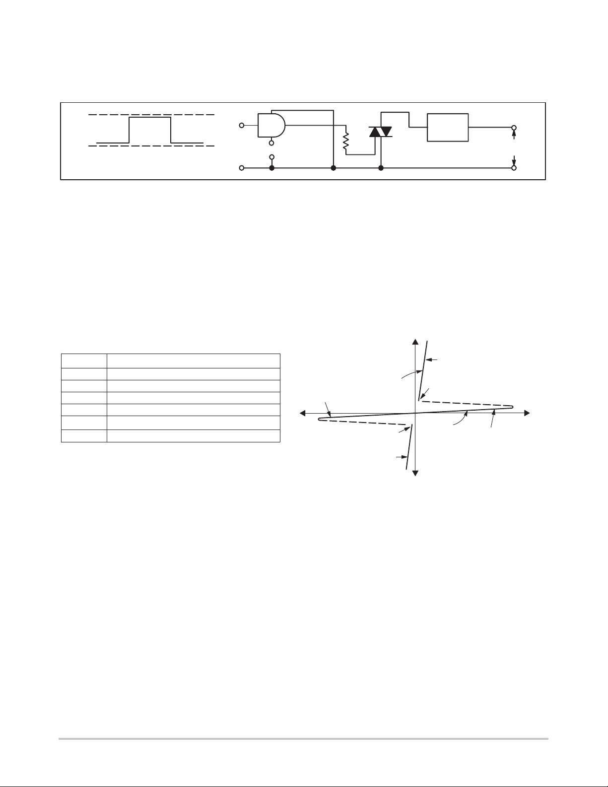
SAMPLE APPLICATION:
TTL-SENSITIVE GATE 4 AMPERE TRIAC
TRIGGERS IN MODES II AND III
0 V
–V
EE
Symbol Parameter
V
DRM
I
DRM
V
RRM
I
RRM
V
TM
I
H
Peak Repetitive Forward Off State Voltage
Peak Forward Blocking Current
Peak Repetitive Reverse Off State Voltage
Peak Reverse Blocking Current
Maximum On State Voltage
Holding Current
14
MC7400
4
7
VEE = 5.0 V
+
Trigger devices are recommended for gating on Triacs. They provide:
1. Consistent predictable turn-on points.
2. Simplified circuitry.
3. Fast turn-on time for cooler, more efficient and reliable operation.
510
Ω
Voltage Current Characteristic of Triacs
(Bidirectional Device)
on state
I
at V
RRM
RRM
Quadrant 3
MainTerminal 2 –
V
TM
2N6071A
+ Current
I
H
LOAD
V
I
H
off state
TM
115 VAC
60 Hz
Quadrant 1
MainTerminal 2 +
I
at V
DRM
DRM
+ Voltage
http://onsemi.com
3
 Loading...