

ON Semiconductor 2N6052G Service Manual
2N6052
Preferred Device
Darlington Complementary
Silicon Power Transistors
This package is designed for general−purpose amplifier and low
frequency switching applications.
Features
• High DC Current Gain — h
= 3500 (Typ) @ IC = 5.0 Adc
FE
• Collector−Emitter Sustaining Voltage — @ 100 mA
V
CEO(sus)
= 100 Vdc (Min)
• Monolithic Construction with Built−In Base−Emitter Shunt Resistors
• This is a Pb−Free Device*
MAXIMUM RATINGS (Note 1)
Rating
Collector−Emitter Voltage V
Collector−Base Voltage V
Emitter−Base Voltage V
Collector Current − Continuous
Peak
Base Current I
Total Power Dissipation @ TC = 25°C
Derate above 25°C
Operating and Storage Temperature
Range
THERMAL CHARACTERISTICS
Characteristic Symbol Max Unit
Thermal Resistance, Junction−to−Case
Stresses exceeding Maximum Ratings may damage the device. Maximum
Ratings are stress ratings only. Functional operation above the Recommended
Operating Conditions is not implied. Extended exposure to stresses above the
Recommended Operating Conditions may affect device reliability.
1. Indicates JEDEC Registered Data.
Symbol Value Unit
CEO
I
P
TJ, T
R
q
CB
EB
C
B
D
stg
JC
100 Vdc
100 Vdc
5.0 Vdc
12
20
0.2 Adc
150
0.857
−65 to +200 °C
1.17 °C/W
Adc
W
W/°C
http://onsemi.com
12 AMPERE
COMPLEMENTARY SILICON
POWER TRANSISTOR
100 VOLTS, 150 WATTS
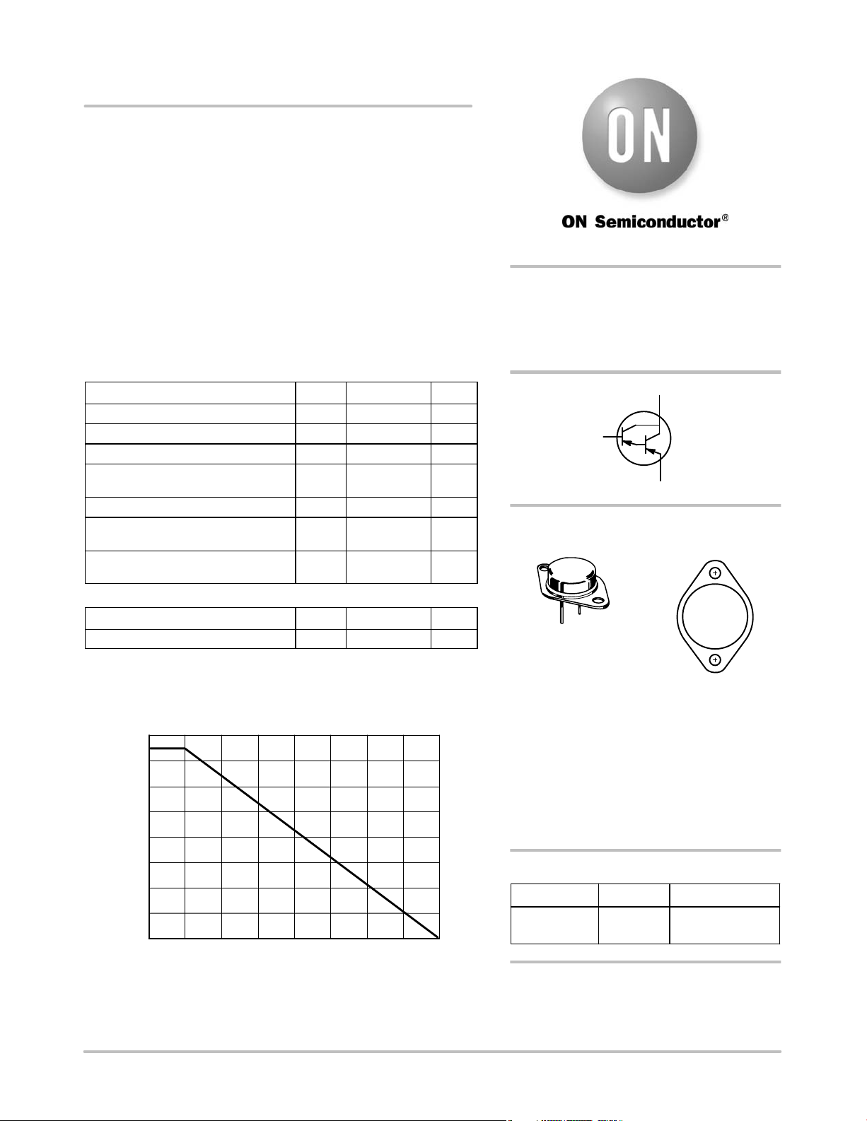
COLLECTOR
CASE
BASE
1
EMITTER 2
MARKING
DIAGRAM
1
2
TO−204AA (TO−3)
CASE 1−07
STYLE 1
2N6052G
AYYWW
MEX
160
140
120
100
80
60
40
, POWER DISSIPATION (WATTS)
D
P
20
0
0 25 50 75 100 125 150 200
TC, CASE TEMPERATURE (°C)
Figure 1. Power Derating
*For additional information on our Pb−Free strategy and soldering details, please download the ON Semiconductor Soldering and Mounting
Techniques Reference Manual, SOLDERRM/D.
© Semiconductor Components Industries, LLC, 2008
September, 2008 − Rev. 5
175
Preferred devices are recommended choices for future use
and best overall value.
1 Publication Order Number:
2N6052 = Device Code
G= Pb−Free Package
A = Location Code
YY = Year
WW = Work Week
MEX = Country of Orgin
ORDERING INFORMATION
Device Package Shipping
2N6052G TO−3
(Pb−Free)
100 Units/Tray
2N6052/D
2N6052
ELECTRICAL CHARACTERISTICS (T
= 25_C unless otherwise noted) (Note 2)
C
Characteristic
OFF CHARACTERISTICS
Collector−Emitter Sustaining Voltage (Note 3) (IC = 100 mAdc, IB = 0)
Collector Cutoff Current (VCE = 50 Vdc, IB = 0)
Collector Cutoff Current
(V
CE
= Rated V
= Rated V
CE
, V
CEO
BE(off)
, V
BE(off)
= 1.5 Vdc)
CEO
= 1.5 Vdc, TC = 150_C)
(V
Emitter Cutoff Current (VBE = 5.0 Vdc, IC = 0)
ON CHARACTERISTICS (Note 3)
DC Current Gain
(I
= 6.0 Adc, VCE = 3.0 Vdc)
C
(IC = 12 Adc, VCE = 3.0 Vdc)
Collector−Emitter Saturation Voltage
(IC = 6.0 Adc, IB = 24 mAdc)
(I
= 12 Adc, IB = 120 mAdc)
C
Base−Emitter Saturation Voltage (IC = 12 Adc, IB = 120 mAdc)
Base−Emitter On Voltage (IC = 6.0 Adc, VCE = 3.0 Vdc)
DYNAMIC CHARACTERISTICS
Magnitude of Common Emitter Small−Signal Short Circuit Forward
Current Transfer Ratio (IC = 5.0 Adc, VCE = 3.0 Vdc, f = 1.0 MHz)
Output Capacitance (VCB = 10 Vdc, IE = 0, f = 0.1 MHz)
Small−Signal Current Gain (IC = 5.0 Adc, VCE = 3.0 Vdc, f = 1.0 kHz)
2. Indicates JEDEC Registered Data.
3. Pulse test: Pulse Width = 300 ms, Duty Cycle = 2.0%.
Symbol
V
CEO(sus)
I
CEO
I
CEX
I
EBO
h
FE
V
CE(sat)
V
BE(sat)
V
BE(on)
|hfe|
C
ob
h
fe
Min
100
−
−
−
−
750
100
−
−
−
−
4.0
−
300
Max
−
1.0
0.5
5.0
2.0
18,000
−
2.0
3.0
4.0
2.8
−
500
−
Unit
Vdc
mAdc
mAdc
mAdc
−
Vdc
Vdc
Vdc
MHz
pF
−
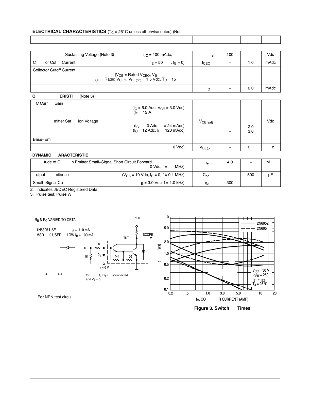
RB & RC VARIED TO OBTAIN DESIRED CURRENT LEVELS
D
MUST BE FAST RECOVERY TYPE, eg:
1
1N5825 USED ABOVE I
MSD6100 USED BELOW I
V
2
approx
+8.0 V
0
V
1
approx
-8.0 V
, tf ≤ 10 ns
t
r
DUTY CYCLE = 1.0%
25 ms
≈ 100 mA
B
≈ 100 mA
B
R
51
for td and tr, D1 is disconnected
and V
= 0
2
B
D
1
+4.0 V
≈ 5.0 k
For NPN test circuit reverse diode and voltage polarities.
Figure 2. Switching Times Test Circuit
TUT
≈ 50
R
V
-30 V
C
CC
10
2N6052
SCOPE
5.0
2.0
t
s
t
f
2N6059
1.0
BE(off)
t
r
= 0
5.0 10
VCC = 30 V
= 250
I
C/IB
= I
I
B1
B2
TJ = 25°C
t, TIME (s)μ
0.5
td @ V
0.2
0.1
0.2
0.5 1.0 3.0 20
IC, COLLECTOR CURRENT (AMP)
Figure 3. Switching Times
http://onsemi.com
2
 Loading...