2N6027, 2N6028
Preferred Device
Programmable
Unijunction Transistor
Programmable Unijunction
Transistor Triggers
Designed to enable the engineer to “program’’ unijunction
characteristics such as RBB, η, IV, and IP by merely selecting two
resistor values. Application includes thyristor–trigger, oscillator , pulse
and timing circuits. These devices may also be used in special thyristor
applications due to the availability of an anode gate. Supplied in an
inexpensive TO–92 plastic package for high–volume requirements,
this package is readily adaptable for use in automatic insertion
equipment.
• Programmable — R
• Low On–State Voltage — 1.5 Volts Maximum @ I
• Low Gate to Anode Leakage Current — 10 nA Maximum
• High Peak Output Voltage — 11 Volts Typical
• Low Offset Voltage — 0.35 Volt Typical (R
• Device Marking: Logo, Device T ype, e.g., 2N6027, Date Code
, η, IV and I
BB
P
= 50 mA
F
= 10 k ohms)
G
http://onsemi.com
PUTs
40 VOLTS
300 mW
G
A
K
MAXIMUM RATINGS (T
Rating Symbol Value Unit
*Power Dissipation
Derate Above 25°C
*DC Forward Anode Current
Derate Above 25°C
*DC Gate Current I
Repetitive Peak Forward Current
µs Pulse Width, 1% Duty Cycle
100
µs Pulse Width, 1% Duty Cycle
*20
Non–Repetitive Peak Forward Current
µs Pulse Width
10
*Gate to Cathode Forward Voltage V
*Gate to Cathode Reverse Voltage V
*Gate to Anode Reverse Voltage V
*Anode to Cathode Voltage
Operating Junction Temperature Range T
*Storage Temperature Range T
*Indicates JEDEC Registered Data
(1) Anode positive, RGA = 1000 ohms
Anode negative, RGA = open
= 25°C unless otherwise noted)
J
(1)
P
1/θ
I
I
TRM
I
TSM
GKF
GKR
GAR
V
AK
stg
1
F
JA
T
G
J
300
4.0
150
2.67
"
50 mA
1.0
2.0
5.0 Amps
40 Volts
*
5.0 Volts
40 Volts
"
40 Volts
–50 to
+100
–55 to
+150
mW
mW/°C
mA
mA/°C
Amps
°C
°C
1
2
3
ORDERING INFORMATION
See detailed ordering and shipping information in the package
dimensions section on page 7 of this data sheet.
Preferred devices are recommended choices for future use
and best overall value.
2
3
TO–92 (TO–226AA)
CASE 029
STYLE 16
PIN ASSIGNMENT
Anode
Gate
Cathode
Semiconductor Components Industries, LLC, 2000
May, 2000 – Rev. 2
1 Publication Order Number:
2N6027/D

2N6027, 2N6028
THERMAL CHARACTERISTICS
Characteristic Symbol Max Unit
Thermal Resistance, Junction to Case R
Thermal Resistance, Junction to Ambient R
Maximum Lead Temperature for Soldering Purposes
(t1/16″ from case, 10 secs max)
θJC
θJA
T
L
75 °C/W
200 °C/W
260 °C
ELECTRICAL CHARACTERISTICS (T
Characteristic
*Peak Current
(VS = 10 Vdc, RG = 1 MΩ) 2N6027
(VS = 10 Vdc, RG = 10 k ohms) 2N6027
*Offset Voltage
(VS = 10 Vdc, RG = 1 MΩ) 2N6027
(VS = 10 Vdc, RG = 10 k ohms) (Both Types)
*Valley Current
(VS = 10 Vdc, RG = 1 MΩ) 2N6027
(VS = 10 Vdc, RG = 10 k ohms) 2N6027
(VS = 10 Vdc, RG = 200 ohms) 2N6027
*Gate to Anode Leakage Current
(VS = 40 Vdc, TA = 25°C, Cathode Open)
(VS = 40 Vdc, TA = 75°C, Cathode Open)
Gate to Cathode Leakage Current
(VS = 40 Vdc, Anode to Cathode Shorted)
*Forward Voltage (IF = 50 mA Peak)
*Peak Output Voltage
(VG = 20 Vdc, CC = 0.2 µF)
Pulse Voltage Rise T ime
(VB = 20 Vdc, CC = 0.2 µF)
*Indicates JEDEC Registered Data
(1) Pulse Test: Pulse Width ≤ 300 µsec, Duty Cycle ≤ 2%.
= 25°C unless otherwise noted.)
C
2N6028
2N6028
2N6028
2N6028
2N6028
2N6028
(1)
Fig. No. Symbol Min Typ Max Unit
2,9,11 I
1 V
1,4,5 I
— I
— I
1,6 V
3,7 V
3 t
P
T
V
GAO
GKS
F
o
r
—
—
—
—
0.2
0.2
0.2
—
—
70
25
1.5
1.0
—
—
— 5.0 50 nAdc
— 0.8 1.5 Volts
6.0 11 — Volt
— 40 80 ns
1.25
0.08
4.0
0.70
0.70
0.50
0.35
18
18
150
150
—
—
1.0
3.0
2.0
0.15
5.0
1.0
1.6
0.6
0.6
50
25
—
—
—
—
10
—
µA
Volts
µA
mA
nAdc
http://onsemi.com
2

2N6027, 2N6028
Adjust
for
Turn–on
Threshold
V
B
Scope
I
A
V
AK
1A –
Programmable Unijunction
with “Program” Resistors
R1 and R2
+V
A
G
K
100k
1.0%
2N5270
20
B
R2
– VS =
R1
–
IP (SENSE)
100 µV = 1.0 nA
+
0.01 µF
Put
Under
Test
I
R1
R1 + R2
A
+
V
B
V
AK
1B –
Equivalent Test Circuit for
Figure 1A used for electrical
characteristics testing
(also see Figure 2)
R
RG =
G
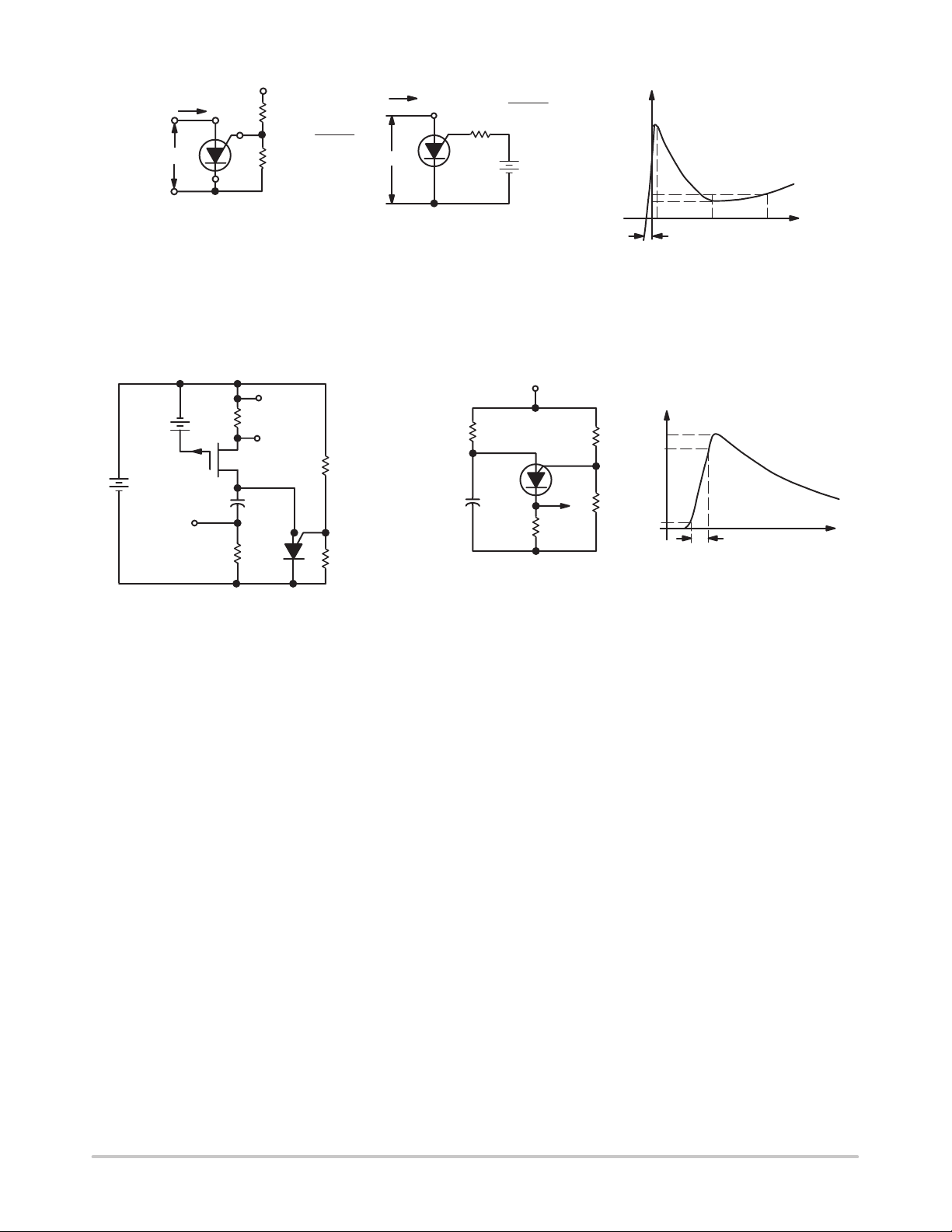
Figure 1. Electrical Characterization
510k
R
RG = R/2
VS = V
B/2
(See Figure 1)
R
C
C
R1 R2
R1 + R2
V
S
+V
20 Ω
V
A
–V
P
V
S
V
F
V
V
I
GAO
B
16k
27k
v
o
0.6 V
VT = VP – V
I
P
IC – Electrical Characteristics
+V
V
o
6 V
t
S
I
V
f
I
I
A
F
t
Figure 2. Peak Current (IP) Test Circuit Figure 3. Vo and tr Test Circuit
http://onsemi.com
3
 Loading...