

Page 1
SERVICE MANUAL
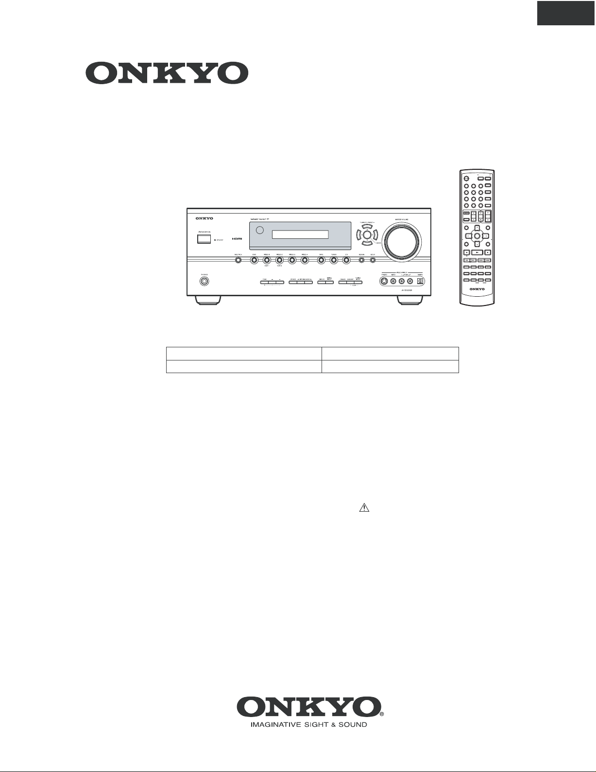
AV RECEIVER
HT-R640
Ref. No. 3951
082006
MODEL
HT-R640
HT-R640 Black, Silver models
B MDD
S MPP
120V AC, 60Hz
230-240V AC, 50Hz
HT-R640
REMOTE MODE
ON/STANDBY
DVD
RECEIVER
TAPE
INPUT SELECTOR
MD/CDR
CD
123
HDD
V1V4V2 V3
TV
456
DVD
MULTI CH
VCR
789
CDTAPE TUNER
CABLE
10 11 12
+
SAT
CLR
10
0
ENT
D TUN
--/---
DIMMER
SLEEP
CH
TV
DISC
VOL
VOL
ALBUM
INPUT
PREVIOUS
GUIDE
MENU
TOP MENU
MUTING
ENTER
PLAYLIST/CAT PLAYLIST/CAT
SETUPRETURN
LISTENING MODE
SURROUND
STEREO
RANDOM
SUBTITLE
AUDIO REPEAT
-
TESTTONE
CH SEL
LEVEL+LEVEL
PLAY MODE
AUDYSSEY
DISPLAY
CINE FLTR
L NIGHT
HDDDVDVCR
-
668M
RC
RC-668M(MDD)
RC-669M(MPP)
SAFETY-RELATED COMPONENT
WARNING!!
COMPONENTS IDENTIFIED BY MARK ON THE
SCHEMATIC DIAGRAM AND IN THE PARTS LIST ARE
CRITICAL FOR RISK OF FIRE AND ELECTRIC SHOCK.
REPLACE THESE COMPONENTS WITH ONKYO
PARTS WHOSE PART NUMBERS APPEAR AS SHOWN
IN THIS MANUAL.
MAKE LEAKAGE-CURRENT OR RESISTANCE
MEASUREMENTS TO DETERMINE THAT EXPOSED
PARTS ARE ACCEPTABLY INSULATED FROM THE
SUPPLY CIRCUIT BEFORE RETURNING THE
APPLIANCE TO THE CUSTOMER.
Page 2
SERVICE PROCEDURE
9
USE
33
R
>
r
USE
2
333GR
>
r
USE
5A-S
50V
8GR
>
910
USE
5A-UL/
33
6GR
910 or
USE
5
2
58GR
USE
50V
GR
9
USE
5A-S
K
8GR
>
3
USE
K
5GR
>
USE
5A-UL/
33
6GR
>
r
USE
50V
5GR
>
r
USE
5
2
58GR
>
1. Replacing the fuses
This symbol located near the fuse indicates that the
fuse used is show operating type, For continued protection against
fire hazard, replace with same type fuse, For fuse rating, refer to
the marking adjacent to the symbol.
Ce symbole indique que le fusible utilise est e lent.
Pour une protection permanente, n'utiliser que des fusibles de meme
type. Ce demier est indique la qu le present symbol est apposre.
<Notes>
<DD> : HT-R640 USA model
: HT-R640 European model
<PP>
HT-R640
REF NO.
01
F
F901 o
01
F
F901 o
F903
F903 o
F90
F903 o
F
F
F6901
F6902
PART NAME
F
F
F
F
F
F
F
F
F
F
F
FUSE
DESCRIPTION
10A-UL/T-2
10A-T/UL-ST
E-EA
E-TL2
T-2
A-T/UL-ST
2.5A-SE-EA
2.5A-SE-TL2
T-2
A-T/UL-ST
12A-TUL-2
12A-TUL-250V
PART NO.
252330G
252
25207
25227
25232
2522
25207
25227
25232
2522
252301
252301GR
REMARKS
!, <DD
!, <DD
!, <PP
!, <PP
!, <DD
!, <DD
!, <PP
!, <PP
!
2. To initialize the unit
1. Press and hold down the VIDEO 1/VCR 1 button, then press the STANDBY/ON button when the unit is Power on.
2. After " Clear " is displayed, the preset memory and each mode stored in the memory are initialized and will return to
the factory settings.
3. To check the version of microprocessor
Main microprocessor Q701 only.
1. Press and hold down the DISPLAY button , then press the STANDBY/ON button when the unit is Power on.
The version is displayed on FL display for 3 seconds.
Ex.
Main1.01/05305A
2. Press the STANDBY/ON button to Power off.
4. Memory Backup
The AV receiver uses a battery-less memory backup system in order to retain radio presets and other settings
when it's unplugged or in the case of a power failure.
Although no batteries are required, the AV receiver must be plugged into an AC outlet in order to charge the
backup system. Once it has been charged, the AV receiver will retain the settings for several weeks,
although this depends on the environment and will be shorter in humid climates.
Page 3
OPERATION CHECK-1
SPEAKER PROTECT-1 (DC VOLTAGE DETECTION)
[When]
1. Exchange power transistors (Q6050 - Q6054, Q6060 - Q6064).
2. Exchange amplifier PC board ass'y (NAAF-8911).
[Procedure]
<Note>
No load. No input.
1. Press and hold down the CD button, then press the STANDBY/ON button while the unit is Power ON.
" Test - _ " is displayed only for 5 seconds.
HT-R640
Test - _
2. Press the VIDEO 3 button, while the characters of " Test - _ " are displayed.
The unit will be in the state of "
Test-4-00
Blinks
".
Test - 4-00
3. Repeatedly press TONE
+ button until the characters of " Test-4-21 " are displayed.
Test - 4-21
Check whether the operation starts and continues automatically as follows.
Test - 4-21
Front L ch
Protect OK
Check
Test - 4-22
Front R ch
Protect OK
Check
Test - 4-23
Center ch
Protect OK
Check
Test - 4-25
Protect OK
Protect
Surround R ch
Check
Test - 4-24
Protect OK
If all channels are OK, the characters of
Test - 4-35
4. Press the STANDBY/ON button.
Clear
Surround L ch
Check
" Test - 4 - 35 "
Turn off
are displayed.
Page 4
OPERATION CHECK-2
SPEAKER PROTECT-2 (CURRENT DETECTION)
[When]
1. Exchange power transistors (Q6050 - Q6054 Q6060 - Q6064.
2. Exchange amplifier PC board ass'y (NAAF-8911).
[Procedure]
<Note>
No input.
Do not check two or more channels at the same time.
Do not connect a dummy load to speaker terminal longer than 2 seconds.
HT-R640
1. Press and hold down the
" Test - _ " is displayed only for 5 seconds.
2. Press the VIDEO 3 button, while " Test - _ " is displayed.
The unit will be in the state of "
CD
button, then press the
Test - _
Test-4-00
".
Blinks
STANDBY/ON
button while the unit is Power ON.
Test - 4-00
3. Repeatedly press
TONE
+
button until
" Test-4-35 " is displayed.
Test - 4-35
4. Connect the dummy load of
At this time, confirm that the speaker relay is
3
ohms to the Front L ch speaker terminal.
not turned off.
Test - 4-35
5. Connect the dummy load of 1 ohm to the Front L ch speaker terminal.
At this time, confirm that the speaker relay is turned off and " Protect " is displayed.
Protect
Disconnect the dummy load immediately after checking the display of
" Protect ".
Test - 4-35
6. Check other channels according to the same procedure as 4 and 5.
7. Press the
STANDBY/ON
button.
Turn off
Clear
Page 5
OPERATION CHECK-3
CONTROL OF POWER SUPPLY (OUTPUT SENSOR AND THERMAL SENSOR)
[When]
1. Exchange power transistors (Q6050 - Q6056, Q6060 - Q6066).
2. Exchange power amplifier PC board ass'y (NAAF-8911).
3. Exchange thermal sensor PC board ass'y (NAETC-8913).
[Procedure]
<Note>
No output. No input.
Output sensor
1. Press and hold down the CD button, then press the
" Test - _ " is displayed only for 5 seconds.
STANDBY/ON
button while the unit is Power ON.
HT-R640
Test - _
2. Press the
The unit will be in the state of "
VIDEO 3
button while
" Test - _ "
Test-4-00
Blinks
is displayed.
".
Test - 4-00
3. Repeatedly press TONE
+
button until
" Test-4-37 " is displayed.
Test - 4-37
4. At this time, confirm that the red characters of
And, check relay RL6901 and RL6902 are
" FM STEREO " is displayed.
turned off in 2 or 3 seconds.
FM STEREO
Test - 4-37
5. Press the STANDBY/ON button.
Clear
Thermal sensor
1. Press and hold down the
" Ver. 0.50/05131a " is displayed only for 2 seconds.
<Ex.>
DISPLAY button, then press the
Ver. 0.50/05131a
Turn off
STANDBY button when the unit is power ON.
TONE
2. Press the
3. Confirm that the displayed temperature is within +/-20 degree C from the ambient temperatures.
4. Press STANDBY/ON button.
button while " Ver.0.50/05131a " is displayed.
<Ex.>
T: 25 C/ 77 F
Turn off
Clear
Page 6
OPERATION CHECK-4(1/2)
DSP DEBUG MODE
The operation of DSP is able to checked by the information displayed on FL in this debug mode.
This information will help to pursue the cause of trouble.
To set in DSP debug mode
1. Press and hold down the
<Ex.>
DISPLAY button, then press the
The version number of microprocessor is displayed only for 2 seconds.
STANDBY
Ver. 0.50/05131a
1. Press the TONE+ button within 2 seconds above, the version number of DSP is displayed.
<Ex.>
DSP :06421A
button while the unit is power ON.
HT-R640
2. Press the
DISPLAY
<Ex.>
To exit
Press
STANDBY/ON button.
Content of display
2
1
-------------------------------- DIR ------------------------------------
1
UNLOCK
E = UNLOCK
= LOCK
Digital Selector
2
0 = None
1 = OPT 3
2 = OPT 2
3 = OPT 1
4 = COAX 1
5 = COAX 2
6 = HDMI
7
= FRONT
DIR Status
3
D = Digital
A
= Analog
M = Multich
P = Multich PCM
p = PCM Fixed
= DTS Fixed
d
button while
" DSP :06421A"
E1A48K0N/OFFPoO
4
4
Sampling Frequency
and Emphasis
= 32 kHz without Emphasis
32K
= 44.1 kHz without Emphasis
44K
= 48kHz without Emphasis
48K
= 64 kHz
64K
= 88.2 kHz
88K
= 96 kHz
96K
= 176.4 kHz
176
= 192 kHz
192
= 32 kHz with Emphasis
32e
= 44.1 kHz with Emphasis
44e
= 48 kHz with Emphasis
48e
5
CODEC CLOCK MODE
N = Normal
U = Up Sampling
H = High Sampling (Double Rate)
D = Down Sampling
Q
= Quad Rate
6
DIR Detect Type
0 = Analog
1 = PCM
2 = Not PCM
3 = Data
4 = DTS CD (Not used)
5 = Multich
6
= Not Decided
is displayed. The status of DSP and DIR will be displayed.
5 6 8
7 1039
11
------------------ DSP --------------------
DSP Port
7
0 = NIC
1 = DEC
2 = BUSY
= EXEC WAIT
3
8
DSP Sequence
04 = Boot
11 = Restart
FF
= Free
DSP Detect Format
9
P = PCM (Analog)
D = Dolby Digital
d = DTS
A = AAC
? =
UNKNOWN
10
DSP Decode
o = Decode OK
x
= Decode NG
------- Main Micro Processor --------
Mute
11
= Selector IC(Q5501)
0
1
= DSP(Q201)
2
= DIR(Q301)
3
(Normal state)
(Abnormal state)
Page 7
OPERATION CHECK-4(2/2)
DSP DEBUG MODE
Trouble Cause Analysis by Debug Mode
This debug mode will help in digital audio no sound trouble.
Check information on FL display and the related devices or circuits.
HT-R640
Digit no.
on FL
1
4
6
8
9
10
11
Symptom on display
"E" is displayed
Displayed freq. is different
from input
Displayed format is different
from input
"04" or "11" do not change
to "FF"
Displayed format is different
from input
"x" is displayed
This identifies IC which
outputs error
Cause
No input signal to DIR
No input signal to DIR
No input signal to DIR
ROM or RAM error
Input signal to DSP is no good
Interface between DSP and
Micro processor is no good
IC outputs error to main
micro processor
Check
Related devices from digital input to Q301
Related devices from digital input to Q301
Related devices from digital input to Q301
Q281, Q282 & related devices
Related devices from Q301 to Q201
Related devices from Q701 to Q201
Q5501, Q201, Q301 & related devices
Page 8
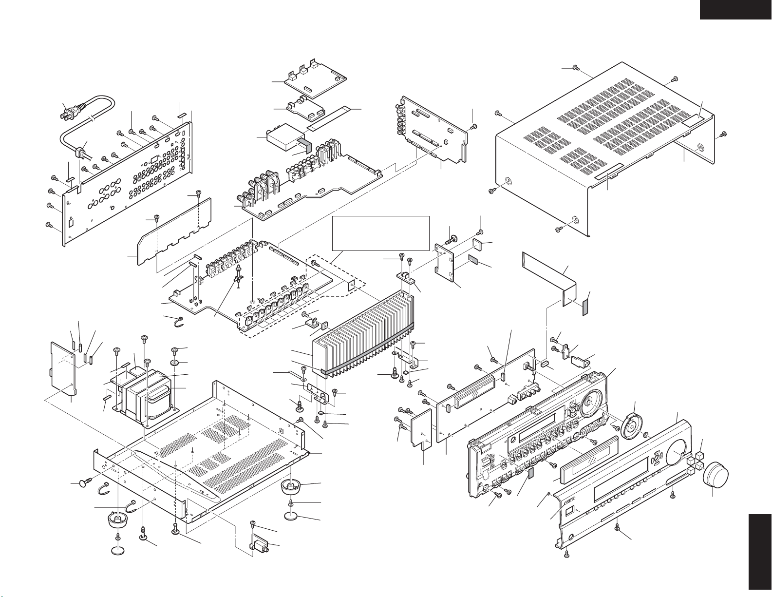
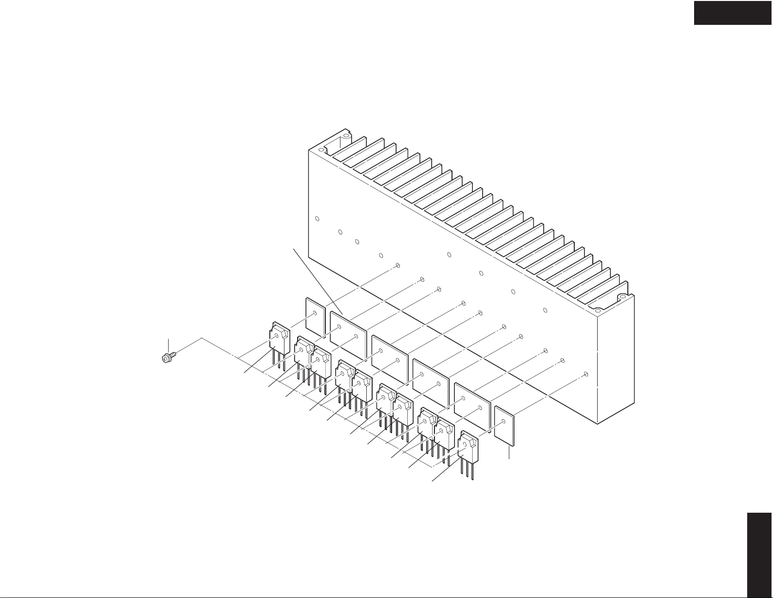
HT-R640
EXPLODED VIEWS-1
P901
A044
F901C
U03
A035
A017
x 2 pcs.
A037
F901
F903C
F910C
U04
F910
A097
x 38 pcs.
A002
A002
U19
F6902
F6901
U15
A013
x 4 pcs.
F903
U16
A020
x 2 pcs.
A044
A093
A018
A030
x 4 pcs.
A031
A033
T901
A021
x 4 pcs.
U14
U010
U21
U13
A028
A051
U17
A040
A044
A041
A045
A016
U06
U18
P101
Refer to
<Fig-1> in
EXPLODED VIEWS-2
A002
x 2 pcs.
A002
A045
A016
x 2 pcs.
A050
A016
x 2 pcs.
A016
A015
A065
x 4 pcs.
A002
x 4 pcs.
A066
x 4 pcs.
A002
x 2 pcs.
U12
A022
U11
A016
A042
A050
A016x 2 pcs.
U01
U02
A002
A002
U10
A002
x 7 pcs.
A002
x 5 pcs.
A052
A053
A050
x 2 pcs.
A051
A070
A081
A077
A061
x 6 pcs.
A102
A060
A109
DD Only
P701
A051
A002
x 2 pcs.
U09
U05
A001
A062
A055
A073
A112
x 4 pcs.
A110
HT-R640
A089
x 3 pcs.
Page 9
EXPLODED VIEWS-2
<Fig-1>
HT-R640
Q6050B
x 4 pcs.
A049
x 10 pcs.
Q6054
Q6064
Q6053
Q6063
Q6052
Q6062
Q6051
Q6061
Q6050
Q6050A
x 2 pcs.
Q6060
HT-R640
Page 10
HT-R640
A
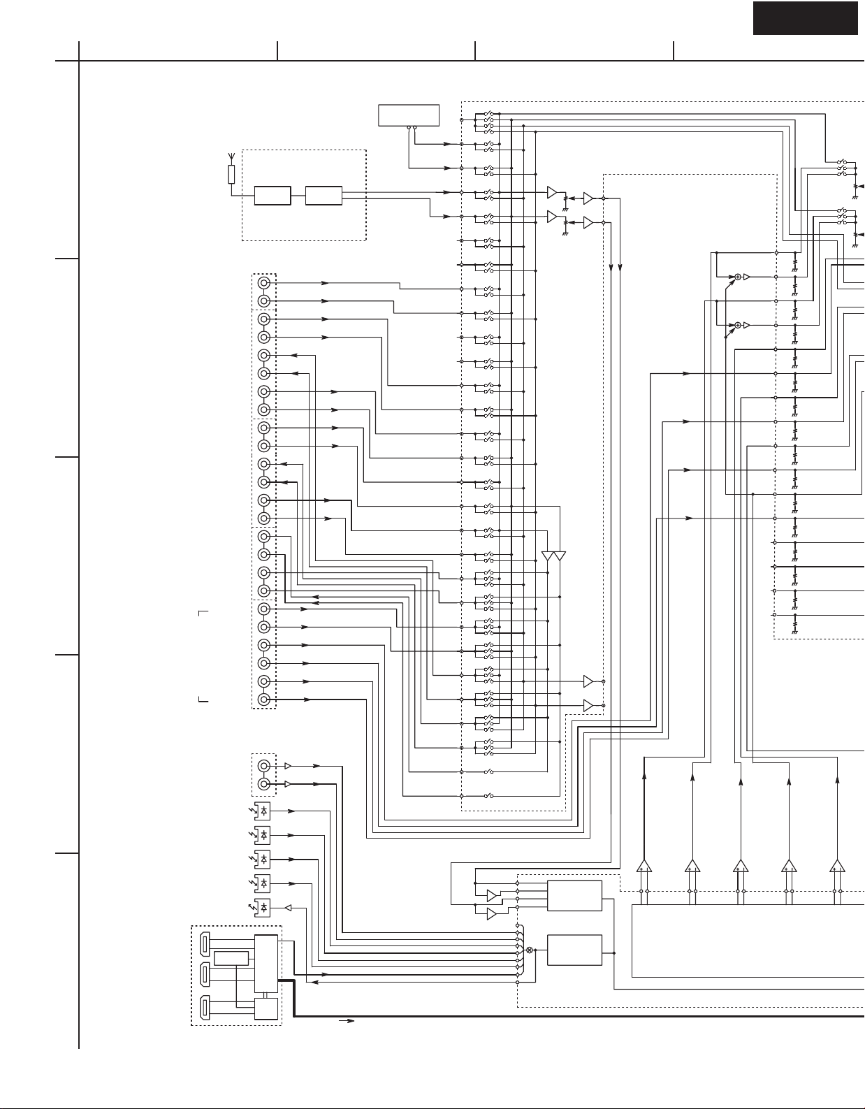
BLOCK DIAGRAM-1
AUDIO SECTION
1
2
3
XM ANTENNA
UNIT
FRONT
VIDEO 4 IN
CD
TAPE OUT
TAPE IN
VIDEO 3 IN
VIDEO 2 OUT
VIDEO 2 IN
VIDEO 1 OUT
VIDEO 1 IN
DVD
INPUT
MULTI CHANNEL
SW
FL
FR
SL
SR
BCDEFGH
FM/AM TUNER UNIT
40
L
59
XM-RADIO
DD ONLY
XM/DT IC
DAC
AK4384
L
R
L
R
L
R
L
R
L
R
L
R
L
R
L
R
L
R
C
R
60
L
63
R
64
65
66
61
62
57
58
55
56
53
54
51
52
49
50
47
48
45
46
71
72
69
MAIN L
MAIN R
SUB L
SUB R
REC L
REC R
37
36
74
INVERTING
35
73
INVERTING
38
39
25k25k 25k25k25k25k
34
75
30
78
25k25k25k25k25k25k25k25k25k25k
33
77
32
76
31
80
29
79
28
4
COAX 1
COAX 2
70
67
68
FR
FL
C
SW
SL
FRONT OPT
OPT 1
OPT 2
OPT 3
OPT OUT
HDMI
RX
HDMI
TX
SPDIF
I2S(DVD-AUDIO)
HDMI
IN 1
IN 2
Micro
Controller
5
OUT
16
15
-
14
13
-
49
43
42
44
46
45
48
47
50
2ch ADC
DIR
Q301 CS42518
LPF
31
LPF
32
30
LPF
33
36
LPF
35
37
LPF
28
34
29
8ch DAC
Page 11
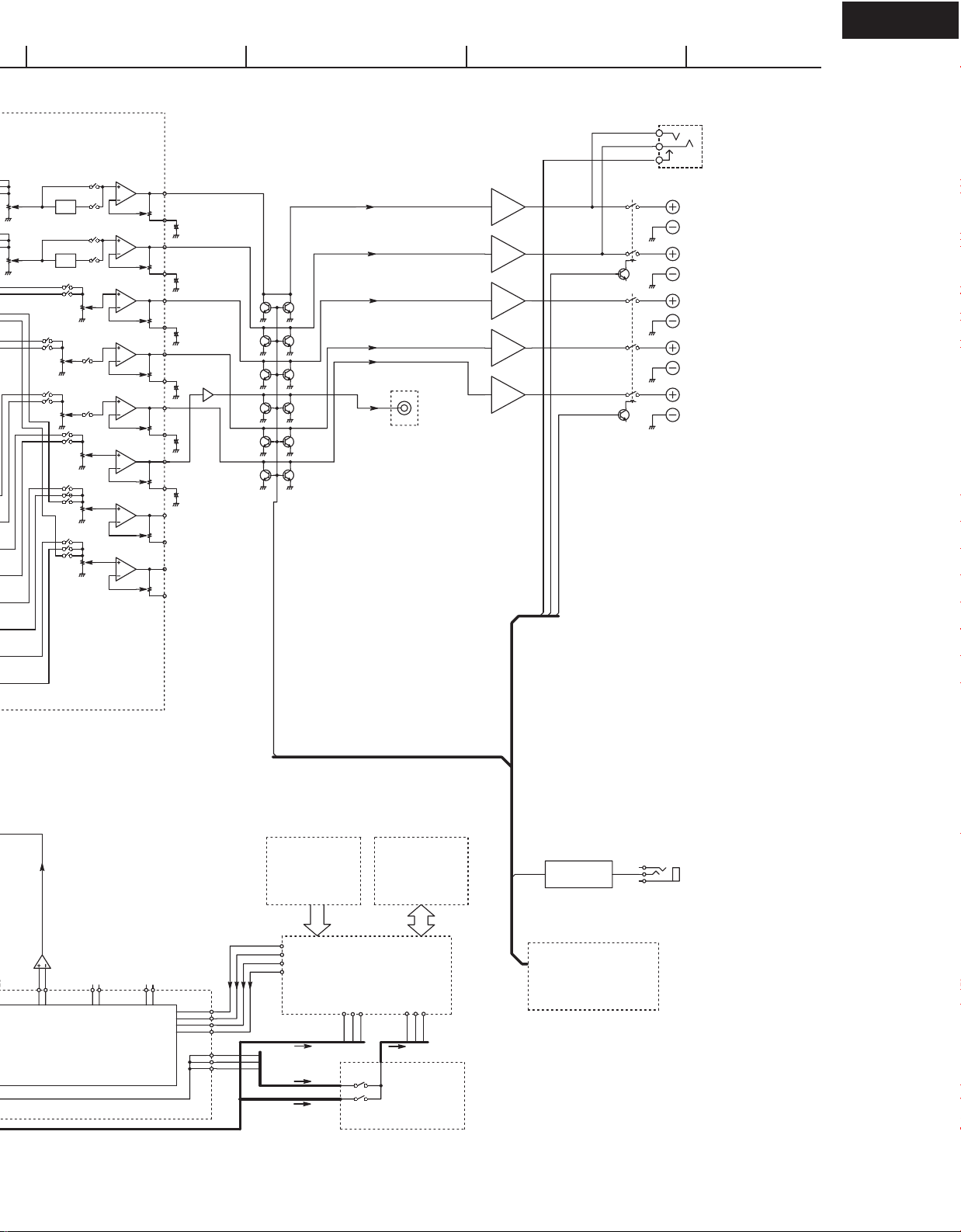
Q5501 R2S15211FP
TONE
TONE
HT-R640
5 CH
POWER
17
16
+
19
20
7
6
+
14
15
+ +++
12
11
9
SW
FL
FR
C
PREOUT
SUB
SL
SR
WOOFER
AMPLIFIER
+29dB
+29dB
+29dB
+29dB
+29dB
HEADPHONES
LEFT
FRONT SPEAKERS
RIGHT
CENTER SPEAKER
LEFT
SURROUND SPEAKERS
RIGHT
SR
10
4
5
2
1
AMUT
SD RAMFLASH ROM
4M Bit
16M bit
HP DET
FRL
CSRL
INTERFACE
RI
RI
117
116
LPF
27
29
22
26
21
23
20
115
113
DSP
TMS320DA707
62
63
64
1
61
60
54
I2S(DVD-AUDIO)
I2S(DIR/ADC)
I2S(DVD-AUDIO)
135
137
TC74VHCT157FT
138
120
139
141
<Note>
Refer to SCHEMATIC DIAGRAM-11(SD-11) for
digital audio signal flow and wave forms.
Q701
M30627FHPGP
MAIN MICRO
PROCESSOR
Page 12
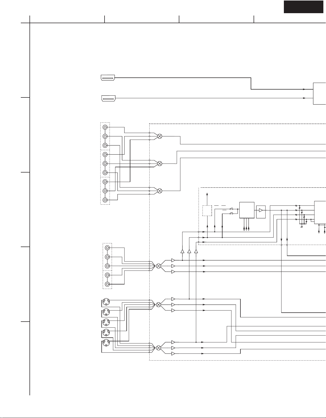
HT-R640
A
BLOCK DIAGRAM-2
VIDEO SECTION
1
HDMI INPUT
COMPONENT
VIDEO INPUT
2
IN1
IN2
IN1
IN2
Y
CB
CR
Y
CB
CR
BCDEFGH
C
V_Y
Q4002 AN-15881A
Y
CB
Y
CB
IN3
CR
CR
3
COMPOSITE
Micro Processor
SDET
SDET*{OSD+(OSD*SI)}
M-SDET
Y
SDET*{OSD+(OSD*SI)}
OSD
Q4004
LC74763
-9836
OSDDA
OSDCS
OSDCK
0dB
DIGITAL VIDEO DECODER
1k
-6dB
1k
1k
-6dB
1k
1k
-6dB
1k
1k
-6dB
1k
Q4001 ADV7183A
Y1
AIN1
COMPOSITE / Y2AIN2
COMPOSITE
AIN3
C1
AIN4
AIN5
C2
SDA
VDRST
VIDEO INPUT
DVD
VIDEO1
VIDEO2
VIDEO3
4
VIDEO4
(FRONT)
S VIDEO INPUT
DVD
YC
YC
VIDEO1
C
Y
V
Y
VIDEO2
VIDEO3
YC
VIDEO4
YC
(FRONT)
C
5
6dB
6dB
6dB
6dB
6dB
6dB
6dB
6dB
6dB
0dB
0dB
0dB
Q4002 AN-15881A
Page 13
HT-R640
Y1
COMPOSITE / Y2AIN2
COMPOSITE
C1
C2
SCL
SDA
HDMI BOARD
DIGITAL VIDEO ENCODER
Q4003 ADV7172
DACA
DACB
DACC
DACD
DACE
DACF
HDMI OUTPUT
Q4002 AN-15881A
Y
CB
CR
COMPONENT
VIDEO OUTPUT
Y
CB
CR
V
Y
C
SDET*{OSD+(OSD*SI)}
SDET*{OSD+(OSD*SI)}
SDET*{OSD+(OSD*SI)}
6dB
6dB
6dB
Y
CB
CR
COMPOSITE
SDET*{OSD+(OSD*SI)}
6dB
SDET*{OSD+(OSD*SI)}
OSD*(SDET + SI)
SDET*OSD
SELV1
SELV2
VIDEO OUTPUT
MONITOR
VIDEO1
VIDEO2
Q4002 AN-15881A
SDET*{OSD+(OSD*SI)}
SDET*{OSD+(OSD*SI)}
6dB
6dB
SDET*{OSD+(OSD*SI)}
SDET*OSD
SDET*OSD
SDET*{OSD+(OSD*SI)}
SDET
SELV1
SELV1
SELV2
SELV2
C
C
C
Y
MONITOR
Y
VIDEO1
Y
VIDEO2
S VIDEO
OUTPUT
Page 14
A
BCDEFGH
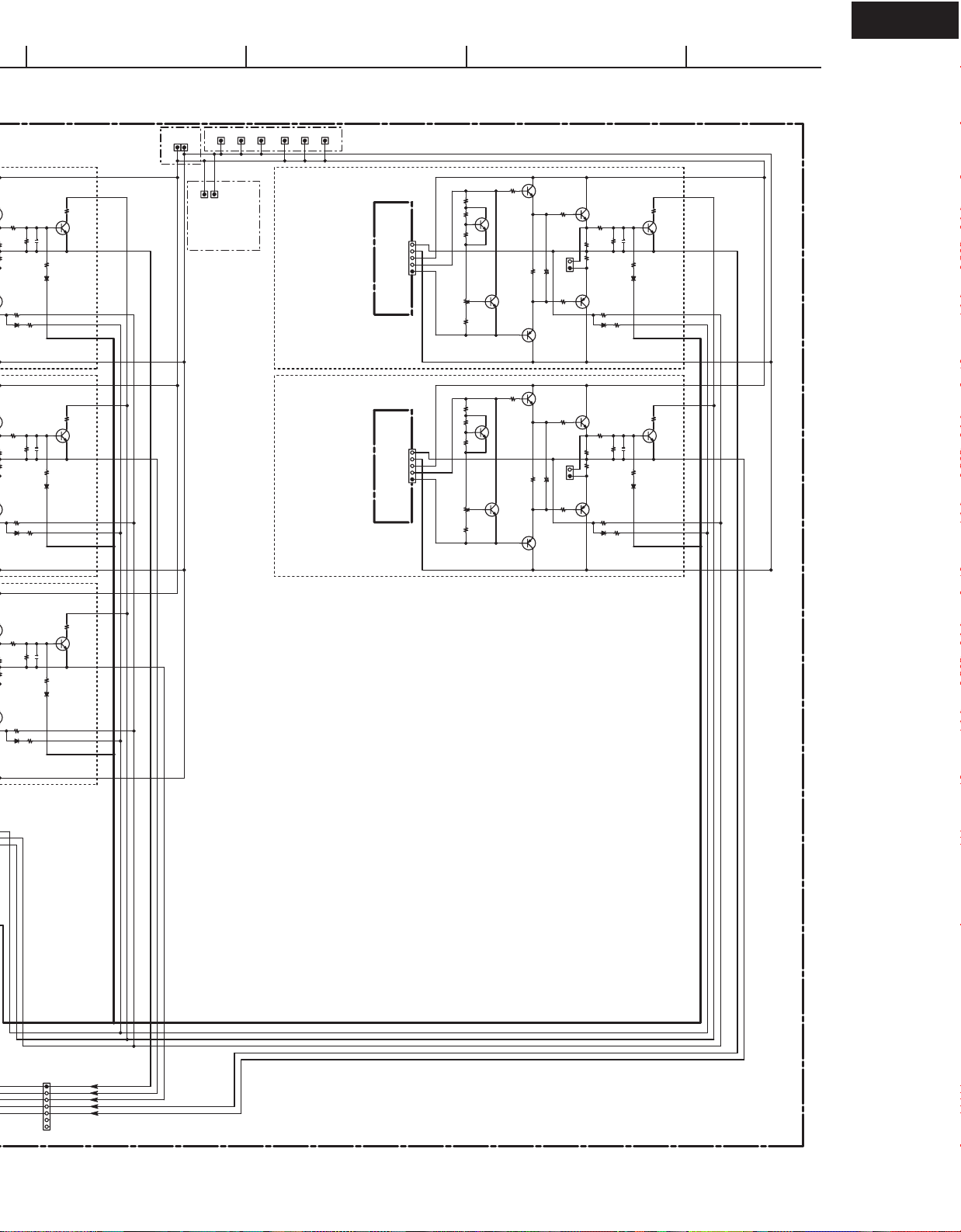
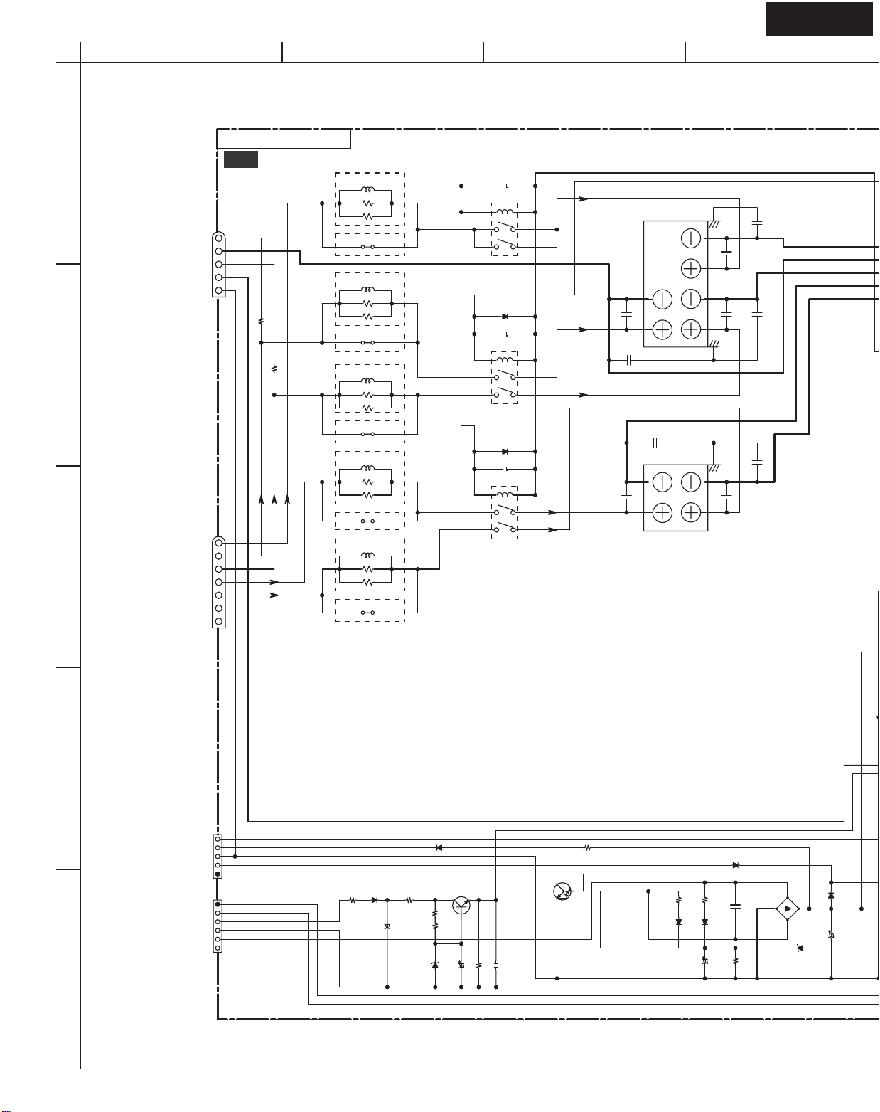
SCHEMATIC DIAGRAM-1(SD-1)
AUDIO SECTION
NAAF-8911 (1/2)
AMPLIFIER PC BOARD
1
2
3
4
U15
CD
TAPE OUT
TAPE
VIDEO 3
VIDEO 2 OUT
VIDEO 2
VIDEO 1 OUT
VIDEO 1
DVD MULTI IN
RI
FR
FL
SW
SR
SL
P5505
R
L
R
L
R
L
R
L
R
L
R
L
R
L
R
L
C
P7900
P7902
P7903
P7904
P7905
R5500
R5504
R5505
R5506
R5508
R5509
R5511
R5512
R5513
R5514
R5515
R5516
R5517
R5518
R5519
R5520
R5521
R5522
R5523
R5524
330
R5503
330
R5543
220K
330
330
330
R5507
330
330
330
R5510
330
330
330
330
330
330
330
330
330
330
330
330
330
330
330
TO NADG-8816
C5701
102J
R5544
220K
R5545
220K
R5546
220K
R5547
220K
R5548
220K
R5549
220K
R5550
220K
R5551
220K
R5552
220K
R5553
220K
R5554
220K
R5555
220K
R5556
220K
R5557
220K
R5558
220K
C5704
102J
R5559
220K
R5560
220K
R5561
220K
R5562
220K
R5563
220K
R5564
220K
C5706
102J
(SD-6:A3)
P304
C5503
221K
C5504
221K
C5507
221J
C5508
221J
C5702
102J
C5509
221J
C5510
221J
C5703
102J
C5513
221J
C5514
221J
C5517
221J
C5518
221J
C5519
221K
C5520
221K
C5521
221J
C5522
221J
C5705
102J
C5523
221J
C5524
221K
C5576
47/50
74
FLIN1
Downmix
47/50
75
FRIN1
R5590
R5594
R5598
123456789
DACR
C5569
77
76
78
CIN1
SLIN1
SRIN1
SWIN1
1-OUT
2-OUT
SBRIN1
3-OUT
4-OUT
5-OUT
6-OUT
FLOUT
FROUT
BASS_R225BASS_R1
BASS_L1
BASS_L2
TRE_L
C5564
223J
Q5503
NE5532
1
10K
C5590
330J
10K
10K
C5591
330J
10K
7
Q5503
TO NADG-8816
(SD-6:A2)
P302
-12V
+12V
GNDA
DACL
DACC
DACSW
GNDDG
79
80
C5551
47/25
1
1-C
SBLIN1
2
3
AGND
4
C5552
47/25
5
2-C
6
C5553
3-C
47/25
7
8
AGND
9
C5554
47/25
10
4-C
C5555
11
5-C
12
47/25
13
AGND
47/25
14
15
C5556
6-C
C5557
16
FLC
17
47/25
18
AGND
19
C5558
47/25
20
FRC
21
C5559
C5560
22
23
C5561
24
223J
2SC1815
AVCC
Q5684
26
7.5V
823J
474J
C5674
470/16
C5562
C5563
C5684
1.8K
R5586
C5685
C5675
470/16
-7.5V
Q5685
2SA1015
4
3
R5591
10K
2
R5593
R5592
1.2K
470
R5597
R5596
470
1.2K
5
R5599
6
10K
8
NE5532
1011121314
VLDATA
VLCLK
PROTECT
823J
220/25
220/25
DAC_FR
DAC_SW
DAC_FL
R5684
R5685
R5675
VOLH
SEC1H
474J
R5585
1.8K
R5674
68
680
D5672
D5671
680
68
AMUT
MTZJ7.5C
MTZJ7.5C
SW_OUT1
R5667
R5666
+12V
22
C5667
C5666
22
-12V
220/25
220/25
+12V
C5630
47/50
C_OUT
SR_OUT
SL_OUT
TO NADG-8816
R5575
R5576
R5577
R5578
R5579
220K
10K
R5587
220K
220K
47K
47K
RI
TUPACKL
(SD-6:A3)
P303
987654321
V4R
V4L
ADLT+
MIC
GNDv4
ADRT+
TUPACKR
GNDTU
65
67
66
64
INL9
63
INR9
62
INLA/RECL1
61
INRA/RECR1
60
INL8
59
INR8
58
INL7
57
INR7
56
INL6
55
INR6
54
INL5
53
INR5
52
INL4
51
INR4
50
INL3
49
INR3
48
INL2
47
INR2
46
INL1
45
INR1
44
AVEE
43
CLOCK
42
DATA
DGND
41
MONO39SUBL38SUBR37ADCR36ADCL35FRIN234FLIN233SRIN232SLIN231SWIN230CIN229SBRIN228SBLIN227TRE_R
40
C5566
R5589
1K
1413121110
DACSBR
DACSBL
DACSL
DACSR
C5574
C5572
C5573
C5575
47/50
47/50
47/50
47/50
71
68
69
70
INL11/RECL5
INR11/RECR5
INLB/RECL2
INRB/RECR2
INR10/RECR4
Q5501
R2S15211FP
(Botom view)
47/25
C5565
47/25
C5571
C5570
47/50
47/50
72
73
RECL3
RECR3
INL10/RECL4
DMIXR
R5595
DMIXL
TO XM
TO NADG-8817
(SD-7:H1)
321
JL5502A
1234567
XM_R
XM_L
GND_AMP
R5581
220K
R5580
220K
R5582
R5583
220K
220K
+12V
-12V
10K
R5588
5
<Note>
SD-x:XY is short for Shcematic Diagram-x and
each socket's location, X=A to H, Y=1 to 5.
Page 15
TO NADG-8816
(SD-6:A2)
P301
65432
1
HT-R640
C5630
47/50
C_OUT
SR_OUT
SL_OUT
L_OUT
R_OUT
R5630
3
3
220
R5631
Q5670
78M12
O
C5672
C5673
O2I
Q5671
79M12
47K
2
220/25
220/25
1
G
G
C5631
15K
I
C5671
1
10/50
3
2
221J
R5632
5
6
4
R5633
1.2K
8
C5670
10/50
Q5630A
NE5532
C5632
Q5630B
NE5532
GND_IR
VOLH
SEC1H
PROTECT
(SD-2)
TO MAIN AMP
R5681
220K
RN1441
Q5600
Q5601
Q5603
2.2K
Q5604
Q5605
2.2K
Q5606
Q5607
2.2K
RN1441
R5620
100
Q5610
RN1441
RN1441
R5623
R5624
0
RN1441
RN1441
R5625
R5626
0
RN1441
R5627
0
0
0
221J
D5707
22K
R5571
C5707
R5531
100
PRE OUT
SW
D5717
C5600
47/50
C5603
47/50
C5604
47/50
C5605
47/50
C5606
47/50
C5607
47/50
R5610
R5600
R5603
R5613
R5614
R5604
R5605
R5615
R5616
R5606
R5607
R5617
270
220K
220K
2.2K
220K
220K
2.2K
220K
220K
SW_OUT
1
R5634
10K
103J
7
SR_OUT
SL_OUT
L_OUT
R_OUT
C_OUT
+12V
R5677
8.2(2W)
R5670
R5678
R5672
47(2W)
R5673
68(2W)
R5671
68(2W)
8.2(2W)
47(2W)
+22V
-22V
C9004
RL1N4003 x4
1000/35
D9002
C9003
D9004
470/35
D9001
D9003
2.2(1W)
C9001
R5660
334J
R5661
2.2(1W)
GND_S1
GND_AMP
S1L+
S1L-
(SD-2:A3)
TO MAIN AMP
(SD-2:B5)
FROM AMP
221J
D5718
D5708
C5708
P7908
SR
SL
13
12
11
10
9
8
7
6
R
5
4
L
3
2
C
1
P5504B
(SD-3:A1)
TO NAAF-8917
P5503B
NOTE
THE COMPONENTS IDENTIFIED BY MARK ARE CRITICAL FOR SAFETY
REPLACE ONLY WITH PART NUMBER SPECIFIED.
VOLTAGE (MEASURED WITH VOLTMETER) IS DC VOLTAGE.(NO INPUT SIGNAL).
ALL PNP TRANSISTORS ARE EQUIVALENT TO 2SA1015-GR UNLESS OTHERWISE NOTED.
ALL NPN TRANSISTORS ARE EQUIVALENT TO 2SC1815-GR UNLESS OTHERWISE NOTED.
ALL DIODES ARE EQUIVALENT TO 1SS133 UNLESS OTHERWISE NOTED.
ELECTROLYTIC CAPACITORS ( ) ARE IN uF/WV.
ALL CAPACITORS ARE IN pF/50WV UNLESS OTHERWISE NOTED.
EX) 030- 3pF 330- 33pF 331- 330pF 333- 0.033uF
ALL RESISTORS ARE IN OHMS 1/4WATTS UNLESS OTHERWISE NOTED.
THE THICK LINES ON PC BOARD ARE THE PRINTING SIDE OF THE PARTS.
EX) PRINTING SIDE
CIRCUIT IS SUBJECT TO CHANGE FOR IMPROVEMENT.
!
Page 16
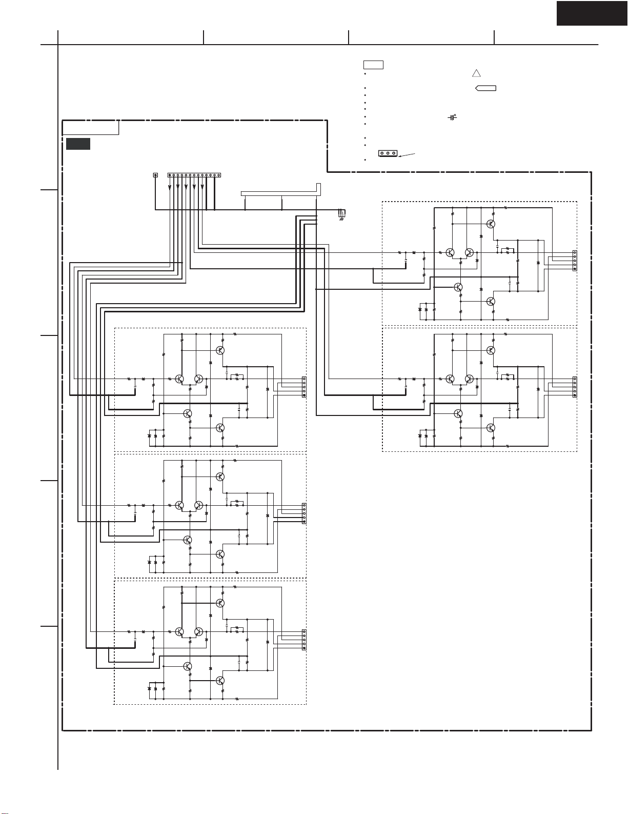
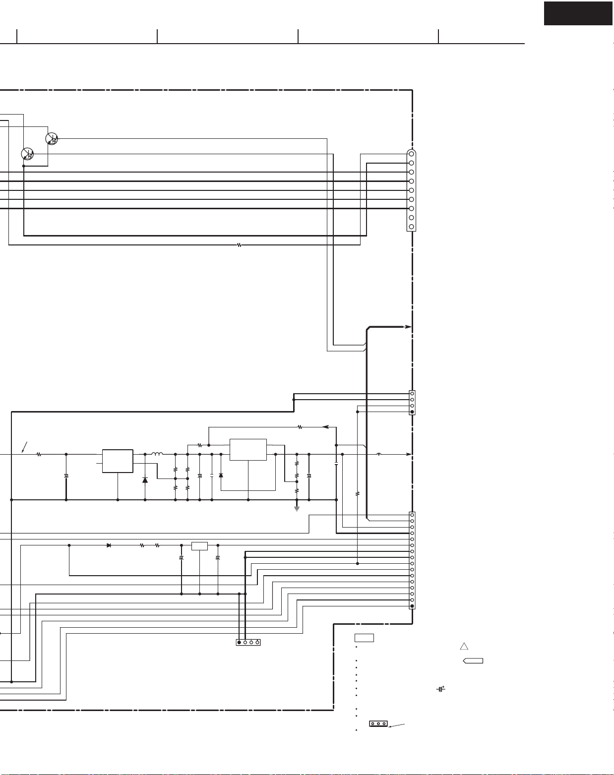
A
SCHEMATIC DIAGRAM-2(SD-2)
POWER AMP SECTION-1
NAAF-8911 (2/2)
BCDEFGH
1
NOTE
THE COMPONENTS IDENTIFIED BY MARK ARE CRITICAL FOR SAFETY
REPLACE ONLY WITH PART NUMBER SPECIFIED.
VOLTAGE (MEASURED WITH VOLTMETER) IS DC VOLTAGE.(NO INPUT SIGNAL).
ALL PNP TRANSISTORS ARE EQUIVALENT TO 2SA1015-GR UNLESS OTHERWISE NOTED.
2
ALL NPN TRANSISTORS ARE EQUIVALENT TO 2SC1815-GR UNLESS OTHERWISE NOTED.
ALL DIODES ARE EQUIVALENT TO 1SS133 UNLESS OTHERWISE NOTED.
ELECTROLYTIC CAPACITORS ( ) ARE IN uF/WV.
ALL CAPACITORS ARE IN pF/50WV UNLESS OTHERWISE NOTED.
EX) 030- 3pF 330- 33pF 331- 330pF 333- 0.033uF
ALL RESISTORS ARE IN OHMS 1/4WATTS UNLESS OTHERWISE NOTED.
THE THICK LINES ON PC BOARD ARE THE PRINTING SIDE OF THE PARTS.
EX) PRINTING SIDE
CIRCUIT IS SUBJECT TO CHANGE FOR IMPROVEMENT.
3
AMPLIFIER PC BOARD
NAETC-8913
U17
THERMAL
SENSOR
PC BOARD
VOLH
SEC1H
GNDS1
+22V
PROTECT
(SD-1:G1 & F4)
FROM AUDIO SECTION
1
JL6402A
T0 NADG-8816
(SD-6:A2)
!
R6701
22K
Q6380
LM61CIZ
G
V
O
2
+5VDIS
THERMAL
GNDDG2
321
10K
R6702
C6703
Q6703
2SA1163-BL
+
1/50
C6704
3
D6703
104Z
R6704
UDZS5.1B
POWER TRANSISTOR LIST
TYPE
Q6050-56
MN130S
DD
2SC5242
PP
33K
R6708
2SC2712-GR
2SC2712-GR
Q6702
Q6701
47K
R6706
220K
D6702
KDS4148U
+
10/50
C6706
D6701
KDS4148U
C6701
5.6K
UDZS5.1B
R6709
D6704
+
100/25
12K
R6710
Q6060-66
MP130S
2SA1962
Center ch
Front L ch
Front R ch
P6000B
5
NF
4
-B1
3
+B1
2
+B
1
-B
T0 NAAF-8917 (SD-3:B3)
P6001B
5
NF
4
-B1
3
+B1
2
+B
1
-B
T0 NAAF-8917 (SD-3:B4)
P6002B
5
NF
4
-B1
3
+B1
2
+B
1
-B
T0 NAAF-8917 (SD-3:B5)
U15
R6040
R6041
R6042
+B1C
1.1V
+BC
R6020
(1/4W)
2.2
470
R6030
1.0V
-0.4V
3.3K
1.0V
3.3K
3.3K
NFC
+BL
NFL
+B1R
+BR
NFR
-BC
-B1C
+B1L
-BL
-B1L
-BR
-B1R
Q6000
2SC1740S-S
Q6010
-1.1V
1.1V
R6021
2.2
Q6001
2SC1740S-S
2SC1740S-S
Q6011
-1.1V
1.1V
R6022
2.2
2SC1740S-S
Q6002
2SC1740S-S
Q6012
-1.1V
0.6V
2SC1740S-S
-0.6V
(1/4W)
0.6V
-0.6V
(1/4W)
0.6V
-0.6V
5.6K
R6000
-0.3V
3.9K
R6010
2K
R6050
470
R6031
5.6K
R6001
-0.3V
3.9K
R6011
-0.4V
2K
R6051
470
R6032
1.0V
5.6K
R6002
-0.3V
3.9K
R6012
-0.4V
2K
R6052
Q6030
2SC5171 or
2SC5993
(1/4W)
82
R6070
Q6040
2SA1930 or
2SA2140
Q6031
2SC5171 or
2SC5993
(1/4W)
R6071
82
Q6041
2SA1930 or
2SA2140
Q6032
2SC5171 or
2SC5993
(1/4W)
R6072
82
Q6042
2SA1930 or
2SA2140
+
C6040
+
C6041
+
C6042
R6080
0.22
(1/4W)
ID+
ID-
47/50
R6090
0.22
(1/4W)
R6081
0.22
(1/4W)
ID+
ID-
47/50
R6091
0.22
(1/4W)
R6082
0.22
(1/4W)
ID+
ID-
47/50
R6092
0.22
(1/4W)
P6080
-54.5V
P6081
P6082
-54.5V
-54.5V
54.5V
2
1
54.5V
2
1
54.5V
2
1
Q6050
LIST
R6140
22K
R6100
0.22(5W)
Q6060
LIST
R6170
47K
D6000
KDS4148U
Q6051
LIST
R6141
22K
R6101
0.22(5W)
Q6061
LIST
R6171
47K
D6001
KDS4148U
Q6052
LIST
R6142
22K
R6102
0.22(5W)
Q6062
LIST
R6172
47K
D6002
KDS4148U
4
NAPS-8912
U16
SEC. TERMINAL-2 PC BOARD
P15-P19 : Power Trans S1 terminal
P6904B(GRN)
P18
P6900B(BLK)
P17 P19
P16
P6903B(YEW)
5
<Note>
SD-x:XY is short for Shcematic Diagram-x and
each socket's location, X=A to H, Y=1 to 5.
P15
JL6952A
1
2
3
4
JL6952B
1
2
3
4
P6903B
P6904B
(1W)
R6197
S1H+
S1H-
F6901
12A 250V
F6902
12A 250V
FROM AUDIO SECTION
100
2SC2712-GR
102J
C6911
S1L+
S1L-
(SD-1:F4)
Q6707
D6902
R6903
4
3 2
3
1SS352
4 1
47K
R6902
1K
RL6902
1
RL6901
2
C6912
334J/100V
C6913
C6915
C6916
D6901
334J/100V
D10XB60H
D10XB60H
104J
D6903
104J
GND_AMP
P6901A
+54.5V
+
C6901
LIST
P6900B
+
LIST
C6902
-54.5V
P6902A
CAPACITOR RATING
MODEL
C6901,C6902
DD
10000uF/63V
10000uF/69V
PP
P6011A
(COPPER BUS PLATE)
GND_SPSL
GND_SPSR
GND_SPR
GND_SPSBL
GND_SPSBR
987654321
R6130-6134
8.2(1W)
C6030-6034
473J(50V)
GND_S1
GND_SPL
GND_SPC
+22V
TO NAVD-8819
(SD-5:G1)
JL6603A
R6132
C6033
C6031
R6130
R6133
R6131
C6032
C6030
R6134
TO NAVD-8819 (SD-5:A3)
C6034
Page 17
HT-R640
Q6050
LIST
R6140
22K
R6100
0.22(5W)
Q6060
LIST
R6170
47K
D6000
KDS4148U
Q6051
LIST
R6141
22K
R6101
0.22(5W)
Q6061
LIST
R6171
47K
D6001
KDS4148U
R6150
R6180
47K
12K
R6181
47K
12K
R6151
C6050
R6190
D6010
C6051
R6191
D6011
R6160
103J
220K
KDS4148U
VPRO
VOLH
R6161
103J
220K
KDS4148U
VPRO
VOLH
Q6070
2SC2240
2SC2240
CLIMP AS
from C6901/6902
to Power Amp of all ch
IPRO
33K
SPC
IPRO
33K
Q6071
SPL
P6901B
-B
P6902B
P6910A
+B
P6902C
P6901C
CLIMP AS
from C6901/6902
to Power Amp
of Surr ch
P6910C
P6910B
P6910E
Surround L ch
Surround R ch
P6910D
P6910F
PVC ASSY
from C6901/6902
to Power Amp of Front ch
P6003B
5
NF
4
-B1
3
+B1
2
+B
1
-B
T0 NAAF-8917 (SD-3:D2)
P6004B
5
NF
4
-B1
3
+B1
2
+B
1
-B
T0 NAAF-8917 (SD-3:D3)
R6043
R6044
+B1SL
1.1V
+BSL
R6023
2.2
R6033
R6003
R6013
R6053
R6034
R6004
R6014
R6054
-0.3V
-0.4V
1.0V
-0.3V
-0.4V
1.0V
NFSL
3.3K
-BSL
-B1SL
+B1SR
+BSR
NFSR
3.3K
-BSR
-B1SR
(1/4W)
Q6003
2SC1740S-S
2SC1740S-S
Q6013
-1.1V
1.1V
R6024
(1/4W)
2.2
Q6004
2SC1740S-S
2SC1740S-S
Q6014
-1.1V
0.6V
-0.6V
0.6V
-0.6V
470
5.6K
3.9K
2K
470
5.6K
3.9K
2K
Q6033
2SC5171 or
2SC5993
(1/4W)
R6073
100
Q6043
2SA1930 or
2SA2140
Q6034
2SC5171 or
2SC5993
(1/4W)
R6074
100
Q6044
2SA1930 or
2SA2140
+
C6043
+
C6044
R6083
0.22
(1/4W)
47/50
R6093
(1/4W)
R6084
(1/4W)
47/50
(1/4W)
ID+
ID-
P6083
0.22
0.22
ID+
ID-
P6084
R6094
0.22
-54.5V
-54.5V
54.5V
2
1
54.5V
2
1
Q6053
LIST
R6143
22K
R6103
0.22(5W)
Q6063
LIST
R6173
47K
D6003
KDS4148U
Q6054
LIST
R6144
22K
R6104
0.22(5W)
Q6064
LIST
R6174
47K
D6004
KDS4148U
R6153
R6183
47K
R6154
R6184
IPRO
33K
R6163
Q6073
2SC2240
12K
103J
C6053
SPSL
220K
R6193
D6013
KDS4148U
VPRO
VOLH
IPRO
33K
R6164
Q6074
2SC2240
12K
103J
C6054
SPSR
220K
R6194
D6014
KDS4148U
VPRO
VOLH
47K
Q6052
LIST
R6142
22K
R6102
0.22(5W)
Q6062
LIST
R6172
47K
D6002
KDS4148U
R6152
R6182
IPRO
33K
R6162
Q6072
2SC2240
12K
103J
C6052
SPR
220K
R6192
D6012
KDS4148U
VPRO
VOLH
47K
TO NAVD-8819 (SD-5:A3)
SPC
1
SPL
2
SPR
3
SPSL
4
SPSR
5
6
7
JL6600A
VOLH
IPRO
VPRO
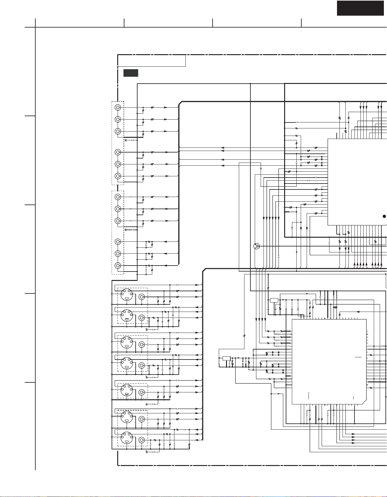
Page 18
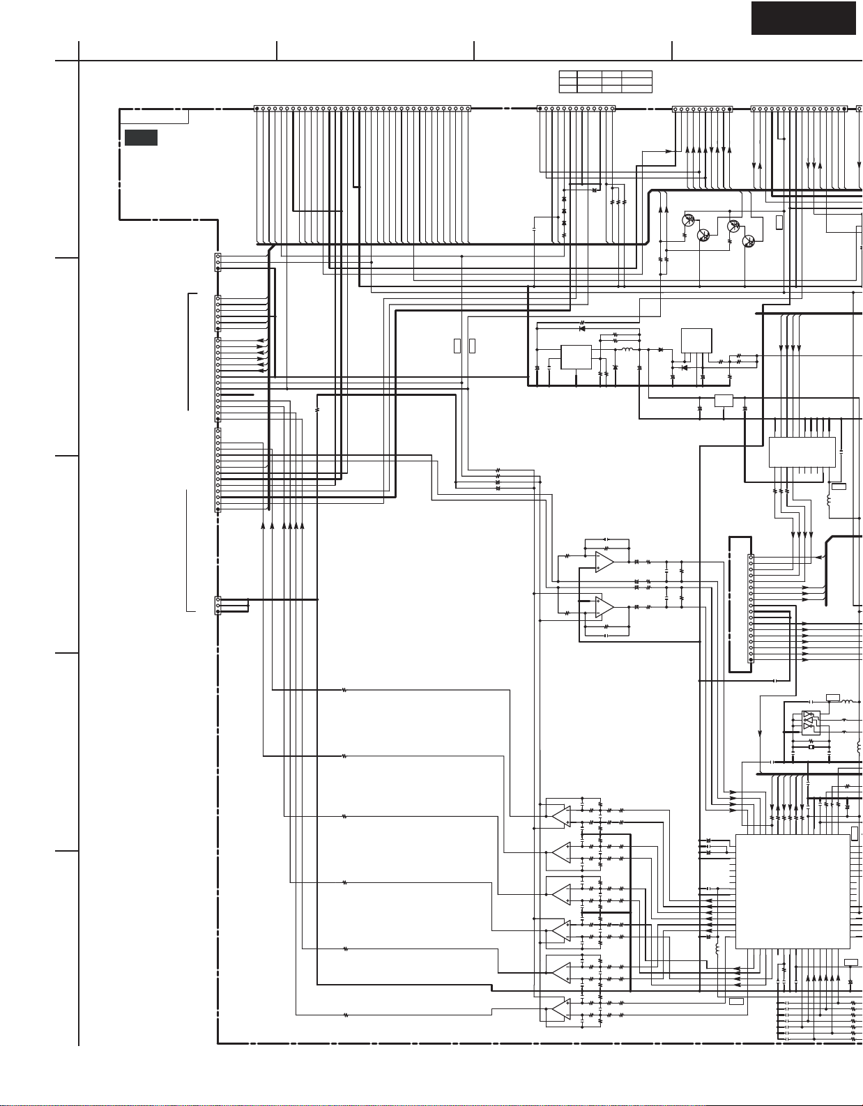
HT-R640
A
SCHEMATIC DIAGRAM-3(SD-3)
POWER AMP SECTION-2
1
NAAF-8917
U19
DRIVER AMPLIFIER PC BOARD
TO NAAF-8911 (SD-1)
P5503A
2
Center ch
R5000
C5010
+
47/50
1K
R5010
221K
C5000
3
R5040
D5000
MTZJ5.6B
Front L ch
C5011
R5001
+
1K
47/50
R5011
C5001
221K
R5041
4
D5001
MTZJ5.6B
Front R ch
C5012
R5002
+
1K
47/50
R5012
221K
C5002
R5042
MTZJ5.6B
5
D5002
P5504A
123
4
56789
101112
13
+53.8V
1K
R5110
100K
R5090
Q5000
2SC2240-BL
R5020
-0.65V
330
56K
R5050
4.7K
2.2K
-48.2V
100K
R5021
330
R5022
330
100K
R5100
-48.2V
100K
R5101
100K
-48.2V
R5102
100K
R5111
Q5001
2SC2240-BL
-0.65V
R5051
4.7K
R5112
Q5002
2SC2240-BL
-0.65V
R5052
4.7K
R5060
R5080
K
1
R5061
R5081
1K
R5062
R5082
1.2K
470
1.2K
470
1.2K
470
10/50
+
C5020
R5091
56K
2.2K
10/50
+
C5021
R5092
56K
2.2K
10/50
+
C5022
+52.3V
Q5010
2SC2240-BL
+
C5040
Q5050
2SC2240-BL
-52.9V
-53.8V
+52.3V
Q5011
2SC2240-BL
C5041
Q5051
2SC2240-BL
-52.9V
-53.8V
+52.3V
Q5012
2SC2240-BL
C5042
Q5052
2SC2240-BL
-52.9V
-53.8V
C5100
C5110
+53.8V
C5101
+
C5111
+53.8V
C5102
+
C5112
+
+
+
+
+
+
0V
220/25
0V
0V
220/25
22/100
22/100
22/100
220/25
22/100
22/100
22/100
R5160
R5170
R5161
R5171
R5162
R5172
100
Q5030
C5080
100
100
Q5031
C5081
100
100
Q5032
C5082
100
(1/4W)
2SA949Y
040D
R5230
120K
Q5040
(1/4W)
(1/4W)
040D
R5231
120K
Q5041
(1/4W)
(1/4W)
040D
R5232
120K
Q5042
(1/4W)
P6011B
(1/4W)
10
R5180
1.1V
R5030
120K
C5090
-1.1V
2SC2229-Y
10
R5190
(1/4W)
10
R5181
1.1V
2SA949Y
R5031
120K
C5091
-1.1V
2SC2229-Y
10
R5191
(1/4W)
10
R5182
2SA949Y
1.1V
R5032
120K
C5092
-1.1V
2SC2229-Y
10
R5192
BCD
R5200
101K
(1/4W)
R5201
101K
(1/4W)
R5202
101K
(1/4W)
18K
R5130
18K
R5131
18K
18K
R5132
COPPER BUS PLATE
+
C5050
47/50
18K
+
C5051
47/50
18K
+
47/50
C5052
NFC
5
4
-B1C
+B1C
3
+BC
2
-BC
1
P6000A
TO NAAF-8911 (SD-2:D1)
NFL
5
-B1L
4
3
+B1L
2
+BL
1
-BL
TO NAAF-8911 (SD-2:D2)
P6001A
NFR
5
4
-B1R
+B1R
3
+BR
2
-BR
1
P6002A
TO NAAF-8911 (SD-2:D3)
NOTE
THE COMPONENTS IDENTIFIED BY MARK ARE CRITICAL FOR SAFETY
REPLACE ONLY WITH PART NUMBER SPECIFIED.
VOLTAGE (MEASURED WITH VOLTMETER) IS DC VOLTAGE.(NO INPUT SIGNAL).
ALL PNP TRANSISTORS ARE EQUIVALENT TO 2SA1015-GR UNLESS OTHERWISE NOTED.
ALL NPN TRANSISTORS ARE EQUIVALENT TO 2SC1815-GR UNLESS OTHERWISE NOTED.
ALL DIODES ARE EQUIVALENT TO 1SS133 UNLESS OTHERWISE NOTED.
ELECTROLYTIC CAPACITORS ( ) ARE IN uF/WV.
ALL CAPACITORS ARE IN pF/50WV UNLESS OTHERWISE NOTED.
EX) 030- 3pF 330- 33pF 331- 330pF 333- 0.033uF
ALL RESISTORS ARE IN OHMS 1/4WATTS UNLESS OTHERWISE NOTED.
THE THICK LINES ON PC BOARD ARE THE PRINTING SIDE OF THE PARTS.
EX) PRINTING SIDE
CIRCUIT IS SUBJECT TO CHANGE FOR IMPROVEMENT.
P5019
Surround L ch
C5013
R5003
+
1K
47/50
C5003
221K
D5003
MTZJ5.6B
R5013
R5043
R5093
100K
R5023
330
56K
2.2K
-48.2V
10/50
+
100K
R5103
C5023
Surround R ch
R5094
100K
C5014
+
47/50
221K
MTZJ5.6B
D5004
R5014
R5044
R5024
330
56K
2.2K
-48.2V
10/50
+
100K
R5104
C5024
R5004
1K
C5004
1K
R5113
Q5003
2SC2240-BL
-0.65V
R5053
4.7K
1K
R5114
Q5004
2SC2240-BL
-0.65V
R5054
4.7K
R5063
R5083
R5064
R5084
+52.3V
Q5053
1.2K
-52.9V
470
+52.3V
Q5054
1.2K
-52.9V
470
-53.8V
Q5013
Q5014
!
+53.8V
+
C5103
22/100
2SC2240-BL
0V
+
220/25
C5043
+
C5113
22/100
2SC2240-BL
-53.8V
+53.8V
+
C5104
22/100
2SC2240-BL
0V
+
220/25
C5044
+
22/100
C5114
2SC2240-BL
R5163
R5173
R5164
R5174
100
Q5033
C5083
Q5043
100
100
Q5034
C5084
120K
100
R5183
(1/4W)
2SA949Y
R5033
120K
040D
R5233
120K
(1/4W)
R5184
10
(1/4W)
2SA949Y
R5034
120K
040D
R5234
Q5044
(1/4W)
(1/4W)
10
1.1V
R5203
101K
C5093
-1.1V
2SC2229-Y
R5193
(1/4W)
10
(1/4W)
1.1V
R5204
101K
C5094
-1.1V
2SC2229-Y
(1/4W)
10
R5194
22K
22K
R5133
22K
22K
R5134
+
C5053
+
C5054
47/50
47/50
NFSL
5
4
-B1SL
+B1SL
3
2
+BSL
1
-BSL
P6003A
TO NAAF-8911 (SD-2:F1)
NFSR
5
4
-B1SR
3
+B1SR
2
+BSR
1
-BSR
P6004A
TO NAAF-8911 (SD-2:F2)
<Note>
SD-x:XY is short for Shcematic Diagram-x and
each socket's location, X=A to H, Y=1 to 5.
Page 19
HT-R640
A
SCHEMATIC DIAGRAM-4(SD-4)
VIDEO SECTION
NAVD-8819 (1/2)
1
PR
COMPONENT
VIDEO IN3
PB
Y
Y
PR
2
COMPONENT
PB
VIDEO IN2
Y
PR
COMPONENT
PB
VIDEO IN1
Y
PR
3
COMPONENT
PB
VIDEO OUT
Y
VIDEO 3 IN
VIDEO 2 OUT
4
VIDEO 2 IN
VIDEO 1 OUT
VIDEO 1 IN
DVD IN
5
MONITOR
OUT
P4001
P4002
P4003
P4004
P4006
P4005
U14
C4019
102K
C4013
102K
YC
YC
YC
YC
YC
C
Y
Y
C
BCDEFGH
VIDEO PC BOARD
C4001
PRIN3
10/50
75
R4001
C4002
PBIN3
10/50
75
R4002
C4003
CYIN3
10/50
75
R4003
PRIN2
C4004
10/50
75
R4004
C4005
PBIN2
10/50
75
R4005
C4006
CYIN2
10/50
75
R4006
PRIN1
C4007
10/50
75
R4007
PBIN1
C4008
10/50
75
R4008
CYIN1
C4009
10/50
75
R4009
C4158
470
C4159
470
C4160
470
R4201
75
R4202
75
R4203
75
C4021
R4015
75
C4219
R4016
R4021
C4162
C4015
102K
102K
R4030
C4020
102K
181J
75
75
101J
75
C4143
100K
R4204
R4205
R4206
R4010
100K
C4014
R4210
R4025
181J
100K
100K
102K
R4213
75
R4014
R4207
R4017
R4020
100K
75
R4022
75
100k
R4011
75
C4218
75
C4161
R4023
R4026
R4029
PROUT
PBOUT
CYOUT
75
181J
75
101J
R4211
75
75
R4027
75
R4214
C4142
181J
C4217
R4208
R4024
C4010
C4011
C4012
10/50
75
R4012
R4013
75
100K
C4016
104Z
C4017
10/50
C4018
10/50
R4018
R4019
75
C4163
100K
C4022
104Z
C4023
10/50
C4024
10/50
75
C4025
104Z
C4026
10/50
C4027
10/50
75
R4028
100k
181J
75
75
104Z
10/50
101J
181J
C4144
CIN_V3
YIN_V3
VIN_V3
COUT_V2
YOUT_V2
VOUT_V2
100K
R4209
CIN_V2
YIN_V2
VIN_V2
COUT_V1
YOUT_V1
VOUT_V1
100K
R4212
CIN_V1
YIN_V1
VIN_V1
CIN_DVD
YIN_DVD
VIN_DVD
C4110
104Z
R4215
100k
PBOUT2
PBOUT
CYOUT2
CYOUT
COUT_MON
YOUT_MON
VOUT_MON
BA33BC0FP
Q4007
1
I
2
C4041
104Z
O
G
C4157
3
102K
LBC2518
L4003
022K
C4042
470/6.3
R9007
103K
C4043
2.2(1/2W)
C4044
GND_VD
+5V_VDD
Q4019
TX-SR574 ONLY
COUT_MON
VOUT
COUT
R4037
C4050
10/16
104Z
C4047
+3.3V
C4053
10/16
C4045
10/16
C4057
104Z
10/16
104Z
C4046
L4010
RN1443
COUT_V2
COUT_V1
YOUT
OSDOUT_1
BA18BC0FP
1
C4028
R4033
1K
R4035
1K
C4035
1K
C4037
C4049
C4051
C4056
R4039
1K
+5V
YOUT_MON
YOUT_V1
YOUT_V2
COUT
+5V_VDD
+5V_VD
R9009
10(1/2W)
Q4006
3
I
O
G
2
104Z
C4156
R4034
C4033
R4036
104Z
104Z
R4038
104Z
C4048
104Z
C4052
C4054
104Z
10/16
104Z
C4055
R4040
1K
C4058
104Z
C4059
L4005
LBC2518
220K
GND_VD
C4122
104Z
C4123
C4124
47/25
C4125
104Z
TX-SR604 ONLY
104Z
C4109
220K
LBC2518
L4002
103Z
470/6.3
C4030
102K
C4029
3.9K
1K
1K
102J
104Z
102K
104Z
C4135
104Z
R4133
75
R4135
75
75
C4103
220/6.3
C4106
220/6.3
C4108
220/6.3
C4111
104Z
C4114
C4116
470/6.3
C4118
470/6.3
C4119
220/6.3
C4121
470/6.3
SDA
VOUT_MON
823J
4.7k
C4034
R4056
1K
R4055
R4057
37
38
36
LEPF
PVDD
^PWRDN
104Z
100
R4041
41
42
C4154
43
221J
44
45
46
47
48
C4155
221J
49
50
51
52
53
54
55
56
57
58
59
60
61
62
63
64
104Z
C4036
C4038
34
32
P133P0
NC35NC
ADV7183B
Video Decoder
R4042
R4043
100
100
PBOUT2
PBOUT1
GND2
CYOUT3-FB
CYOUT3
CYOUT2-FB
CYOUT2
COUT4
VCC2
COUT3
COUT2
COUT1
GND3
YOUT4-FB
YOUT4
YOUT3-FB
YOUT3
YOUT2-FB
YOUT2
YOUT1
VCC3
VOUT4-FB
VOUT4
SDA
220J
C4167
103K
30
31
DVDD
DGND
Q4001
C4061
103K
080D
C4039
X4003
29
XTAL
C4062
R4134
C4104
220/6.3
C4105
22/50
C4107
22/50
47/25
C4112
104Z
470/6.3
+5V
220J
C4168
L4001
YOUT
RN72K2E-022JE
LBC2518
L4004
022K
+1.8V
680
104Z
103J
C4031
C4032
39
AGND40AGND
41
AIN7
42
AIN1
43
AIN8
44
AIN2
45
AIN9
46
AIN3
47
AGND
48
CAPY1
49
CAPY2
50
AVDD
51
REFOUT
52
CML
53
AGND
54
CAPC1
55
CAPC2
56
AGND
57
AIN10
58
AIN4
59
AIN11
60
AIN5
AIN1262AIN663NC64RESET65NC66ALSB67SDA68SCLK69NC70NC71DGND72DVDD73P1574P1475P1376P1277NCC78NC79OE80FIELD
61
C4060
PROUT2
PROUT
33
PRIN1
PRIN2
PRIN3
R4136
C4133
220/6.3
C4134
220/6.3
30
36
37
38O139
40
O2
PROUT1
PROUT2
MUTE
PR131PR232PR333PR434PR535PR6
Q4002
AN-15881A-VT
Video Switch
VOUT3-FB66VOUT367VOUT2-FB68VOUT269VOUT170SCL71V172V273V374V475V576V677V778V879Y180Y2
65
C4130
C4127
470/6.3
VOUT_V2
080D
C4040
28.6363MHz
R4054
33
FCX-03
26
28
XTAL1
104Z
C4129
VOUT_V1
VOUT
25
NC
LLC227LLC1
220/6.3
470/6.3
VIN_DVD
DVDDIO
DVDDIO
DGND
INTRQ
DVDD
DGND
DGND
VIN_V1
VIN_V2
21
P522P423P324P2
P6
P7
NC
NC
NC
NC
SFL
P8
P9
P10
P11
HS
VS
VIN_V4
VIN_V3
20
19
18
17
16
15
14
13
R4053
12
11
10
9
8
7
6
5
4
3
2
1
R4052
C4131
AGND
33
33
C4132
104Z
OSDOUT_1
VIN_DAC
PBIN3
25
BP226PB327PB428PB529PB6
10/50
YIN_V1
YIN_DVD
104Z
PBIN2
BIAS
GND1
VCC1
PB1
CY6
CY5
CY4
CY3
CY2
CY1
C4063
Page 20
HT-R640
25
PB3
Y180Y2
YIN_V1
104Z
BP2
PBIN2
BIAS
GND1
VCC1
PB1
CY6
CY5
CY4
CY3
CY2
CY1
C8
C7
C6
C5
C4
C3
C2
C1
Y8
Y7
Y6
Y5
Y4
Y3
+5V_VD
C4065
104Z
C4064
104Z
C4063
C4176
C4177
C4244
C4243
C4178 104Z
24
C4242
23
22
104Z
21
20
19
18
C4136
17
16
C4150
15
C4137 104Z
14
13
12
11
10
9
8
C4138
7
6
C4139
5
10/50
C4140
4
104Z
3
2
1
L4011
+5V_VDD
R4159
10k
Q4018
RN1401
104Z
104Z
104Z
104Z
22/50
104Z
104Z
C4141
47/25
2SK3019
Q4008
R4031
Q4009
2SK3019
R4032
TO NADG-8816 (SD-6:D1)
GND_VD
104Z
104Z
C4148
C4149
VMUT
PRIN_DAC
PBIN_DAC
PBIN1
CYIN_DAC
CYIN3
CYIN2
CYIN1
COUT
CIN_DAC
CIN_V4
CIN_V3
CIN_V2
CIN_V1
CIN_DVD
OSDOUT_2
YIN_DAC
YIN_V4
YIN_V3
YIN_V2
COFF
SCL
SDA
VDRST
VSYNC
SCL
SDA
D
G
S
D
G
0
R4058
S
2.2k
0
Q4010
RN1401
R4061
R4060
4.7K
R4051
R4050
R4049
R4048
R4047
R4046
R4045
R4044
L4006
LBC2518
022K
P2004B
987654321
10
104Z
10/50
10/50
GND_VD
C4152
C4151
C4153
YIN_V4
VIN_V4
CIN_V4
SYCDET
OSDCS
OSDDA
OSDCK
COFF
SDET
OSDOUT_1
OSDOUT_2
VOUT
SELV
YOUT
SELY
R4059
2.2k
100
+3.3V
1
33
2
33
3
33
4
33
5
6
33
7
33
8
33
9
33
10
C4069
11
104Z
12
C4070
10/16
SCL
SDA
180J
180J
Q4016
RN1443
Q4015
RN1443
VAA
P0
P1
P2
P3
P4
P5
P6
P7
CSO_HSO
VAA
GND
C4071
104Z
VSYNC
SDET
VMUT
VDRST
14.23MHz
X4001
C4079
100D
C4080
C4081
C4082
17.73MHz
X4002
080D
2.2K
R4100
2.2K
R4101
2.2K
R4102
470J
C4083
R4128
33
C4086
1/50
104Z
104Z
C4066
C4067
47
43
45
48
44
46
VSO
VAA
GND
RESET
CLOCK
PAL NTSC
Q4003
ADV7172
Video Encoder
GND14HSYNC15FIELD/VSYNC
BLANK17ALSB18GND19VAA20SCLOCK21SDATA22RSET223COMP224DAC F
16
13
4.7K
R4075
R4074
470J
C4084
42
CLAMP
4.7K
470J
220
R4125
41
TTX
R4076100
R4063
40
R4077100
OSD
1
VSS
2
XTALIN1
3
XTALOUT1
4
HSYNCOUT
5
XTALIN2
6
XTALOUT2
7
VSYNCOUT
8
CS
9
SIN
10
SCLK
11
SW1
12
SW2
13
C4085
SW3
14
SW4
15
RST16CVOUT
220
R4124
Q4014
2SA1162-GR
2SA1162-GR
1.2K
1.2K
R4064
C4068
39
37
38
VREF
RSET1
COMP1
TTXREQ
DAC A
SCRESET/RTC
DAC B
DAC C
DAC D
DAC E
R4079
R4078
1.2K
1.2K
TO NADG-8816 (SD-6:D1)
R4147
2.7k
1SS352
D4142
30
VDD1
29
SYNCDET
28
CVCOOUT
27
VCOIN
26
FC
R4104
25
AMPOUT
120
24
AMPIN
R4107
23
PDOUT
1.5K
22
VSS
21
SEPC
20
SYNCIN
19
R4108
CVCR
820K
18
Q4004
CVIN
17
VDD2
LC74763-9836
220
220
R4120
R4121
12k
R4118
Q4013
104Z
VAA
VAA
GND
VAA
VAA
GND
C4072
104Z
36
35
34
33
32
31
30
29
28
27
26
25
+3.3V
104Z
C4073
R4084
C4076
105K
R4088
R4092
C4165
104Z
R4068
R4080
C4074
C4075
104Z
68
C4077
104Z
R4096
P2006B
987654321
10
SPRLB
SPRLSB
SPRLCS
SELY
SPRLF
C4147
0.47/50
C4087
47k
R4148
474J
022K
L4008
C4088
L4009
C4089
056J
C4090
R4103
1K
R4106
C4092
6.8K
C4093
R4109
0.33/50
C4094
C4096
470/6.3
C4097
C4095
470J
104Z
C4099
100/16
Q4012
2SA1162-GR
C4102
104Z
2.7k
R4119
R4065
100
R4067
68
82
R4081
82
68
R4082
100
104Z
R4085
68
82
R4086
100
100
R4090
R4089
82
R4094
100
82
R4093
68
R4098
C4078
105K
100
R4097
82
68
SELV
C4175
R4117
101J
OSDCS
SYCDET
C4091
682J
220
122K
33k
OSDCK
OSDDA
+5V_VDD
022K
L4007
LBC2518
1/50
R4105
R4112
+5V_VD
68
R4114
D4001
C4101
104Z
R4116
2.2K
CYIN_DAC
C4170
101J
C4171
101J
PBIN_DAC
C4172
101J
PRIN_DAC
VIN_DAC
C4173
101J
YIN_DAC
C4174
101J
CIN_DAC
TO SD-5:G3
L4009
NCH-1572
L4008
LBC2518
C4088
C4089
C4090
6.8K
Q4017
2SC2712-GR
1K
R4110
3.3K
47K
R4111
C4100
1SS352
1
D4002
1SS352
270J
220J
223J
100/16
C4098
10K
R4113
104Z
Q4011
10K
R4115
+5V_VDD
+5V_VD
RN2402
NOTE
THE COMPONENTS IDENTIFIED BY MARK ARE CRITICAL FOR SAFETY
REPLACE ONLY WITH PART NUMBER SPECIFIED.
VOLTAGE (MEASURED WITH VOLTMETER) IS DC VOLTAGE.(NO INPUT SIGNAL).
ALL PNP TRANSISTORS ARE EQUIVALENT TO 2SA1015-GR UNLESS OTHERWISE NOTED.
ALL NPN TRANSISTORS ARE EQUIVALENT TO 2SC1815-GR UNLESS OTHERWISE NOTED.
ALL DIODES ARE EQUIVALENT TO 1SS133 UNLESS OTHERWISE NOTED.
ELECTROLYTIC CAPACITORS ( ) ARE IN uF/WV.
ALL CAPACITORS ARE IN pF/50WV UNLESS OTHERWISE NOTED.
EX) 030- 3pF 330- 33pF 331- 330pF 333- 0.033uF
ALL RESISTORS ARE IN OHMS 1/4WATTS UNLESS OTHERWISE NOTED.
THE THICK LINES ON PC BOARD ARE THE PRINTING SIDE OF THE PARTS.
EX) PRINTING SIDE
CIRCUIT IS SUBJECT TO CHANGE FOR IMPROVEMENT.
!
TO SD-5:G3
<Note>
SD-x:XY is short for Shcematic Diagram-x and
each socket's location, X=A to H, Y=1 to 5.
Page 21
HT-R640
A
SCHEMATIC DIAGRAM-5(SD-5)
SPEAKER OUT SECTION
NAETC-8819 (2/2)
U14
1
JL6605B
NAETC-8790 (SD-8:B5)
2
3
JL6600B
TO NAAF-88911 (SD-2:E2)
VIDEO PC BOARD
01
HPL
02
LSPE
03
HPR
04
05
HPDET
R6691
MPUGND
390(1/2W)
R6992
390(1/2W)
LSP
01
02
03
04
05
06
07
CSP
RSP
SLSP
SRSP
BCDEFGH
PP-TYPE
L6602 S1.3C
R6602 22
22
R6612
J6851
DD-TYPE
PP-TYPE
L6600 S1.3C
R6600 22
22
R6610
J6600
DD-TYPE
PP-TYPE
S1.3C
L6601
22
R6601
R6611
22
J6604
DD-TYPE
PP-TYPE
S1.3C
L6603
22
R6603
22
R6613
J6619
DD-TYPE
PP-TYPE
L6604
S1.3C
22
R6604
R6614
22
J6620
DD-TYPE
C6602
223Z
RL6602
6
2
D6600
1SS352
C6600
223Z
RL6600
6
2
D6603
1SS352
C6603
223Z
RL6603
6
2
5 4
FRONT SPEAKERS
1
3
45
C6640
1
3
45
1
3
C6650
102J
C6643
103J
103J
C6653
102J
L
SL
P6601
P6602
SR
102J
C6652
C
R
103J
C6642
102J
103J
C6651
C6641
5 8
10
C6644
103J
C6654
102J
DTC123JKA
SURROUND SPEAKERS
4
TO NAPS-8787
TO NAETC-8788
5
<Note>
SD-x:XY is short for Shcematic Diagram-x and
each socket's location, X=A to H, Y=1 to 5.
5
4
3
2
JL901B
(SD-9:F1)
1
1
2
3
4
5
JL9101B
6
(SD-9:G2)
POFF
+12VD
MPUGND
FLAC1
FLAC2
SEC3-1
SEC3-2
SEC2-1
SEC2-2
+10S
POWERD
R9010
82(1/2W)
RL1N4003
D9002
+
C9001
R9005
220(1/2W)
470/63
D9013
1SS352
8.2K
R9003
D9005
Q9001
2SC2235-Y
8.2K
R9006
C9005
UDZS36B
47/50
R9004
33K
+5VDIS
223Z
C9006
R9011
4.7(1/2W)
APOWER
SEC2-1
Q9002
RN1405
-VP
SEC2-2
1SS352
1
R9013
D9015
1SS352
C9013
1
R9012
D9014
3.3/50
1SS352
D9012
C9012
334J
100k
R9014
3
D9017
1
D9011
C9011
1SS352
POFF2
10000/16
4
D5SBA20
2
UDZS5.6B
D9024
Page 22
Q6602
Q6601
DTC123JKA
SPRLF
SPRLCS
R6690
10(1/2W)
RLGND
+24V
+24V
RLGND
CSPE
LSPE
RSPE
SLSPE
SRSPE
01
02
03
04
05
06
JL6603B
07
08
TO NAAF-8911 (SD-2:D5)
09
HT-R640
DD:+12V
PP:+10V
R9028
0.47(1/2W)
+
C9021
470/16
1
VIN
5
SS
D9022
RL1N4003
Q9021
SI-8008
GND
TO SD-4:G1
SPRLCS
SPRLF
GND_HD
PP-TYPE
(PURE AUDIO)
Q9022
C9024
3
223Z
+
C9032
1
2
D9020
1SS352
470/6.3
BA00JC5WT
Vc
Vin
GND
3
GND_VD
Adj
Vo
+6V
R9002
R9020
R9021
10k
R9027
1.5k
R9008
MPC2905HF
+
C9031
470/16
DD-TYPE
R9018
0
10k
C9023
1.5k
Q9031
1
I
2
+
O
G
470/6.3
NCH-2541_470K
L9001
2
SW
4
VADJ
3
R9001
D9021
3.3(2W)
CRS09
3.3(2W)
R9017
0
5
4
100k
R9022
6.8k
R9023
33k
R9024
+
+5V_VD
C9025
470/6.3
VPOWER
223Z
C9022
R9029
0.47(1/2W)
L4015
LBC2518
HPDET
VPOWER
+5V_XM
GND_XM
+5VDIS
+5VDSP
GND_VD
GND_VD
+10VDSP
POFF
POFF2
APOWER
10S+12VD
-VP
FLAC1
FLAC2
047K
+5V_VDD
4
3
2
1
JL8001A
TO NAVD-8928 (SD-10 :B1)
TO SD-4G3
16
15
14
13
12
11
10
9
8
P2005B
7
6
5
TO NADG-8816 (SD-6:D1)
4
3
2
1
1
Q9031A
432
NOTE
THE COMPONENTS IDENTIFIED BY MARK ARE CRITICAL FOR SAFETY
REPLACE ONLY WITH PART NUMBER SPECIFIED.
VOLTAGE (MEASURED WITH VOLTMETER) IS DC VOLTAGE.(NO INPUT SIGNAL).
ALL PNP TRANSISTORS ARE EQUIVALENT TO 2SA1015-GR UNLESS OTHERWISE NOTED.
ALL NPN TRANSISTORS ARE EQUIVALENT TO 2SC1815-GR UNLESS OTHERWISE NOTED.
ALL DIODES ARE EQUIVALENT TO 1SS133 UNLESS OTHERWISE NOTED.
ELECTROLYTIC CAPACITORS ( ) ARE IN uF/WV.
ALL CAPACITORS ARE IN pF/50WV UNLESS OTHERWISE NOTED.
EX) 030- 3pF 330- 33pF 331- 330pF 333- 0.033uF
ALL RESISTORS ARE IN OHMS 1/4WATTS UNLESS OTHERWISE NOTED.
THE THICK LINES ON PC BOARD ARE THE PRINTING SIDE OF THE PARTS.
EX) PRINTING SIDE
CIRCUIT IS SUBJECT TO CHANGE FOR IMPROVEMENT.
!
Page 23
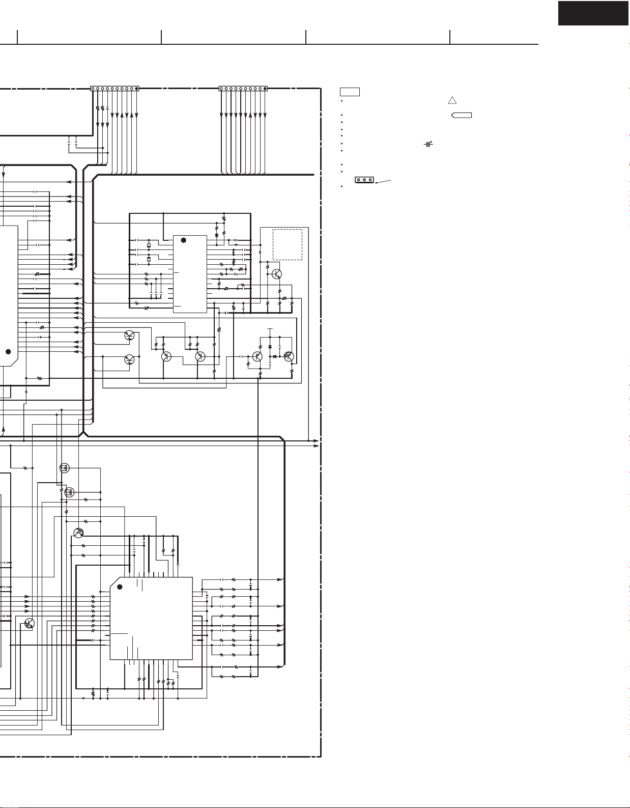
A
SCHEMATIC DIAGRAM-6(SD-6)
DSP SECTION
NADG-8816
U12
1
DSP PC BOARD
2
3
4
5
THERMAL
3
JL6402B
+5VDSP
2
GNDDG
1
(SD-2:B2)
TO NAETC-8913
SBZ2MUT
6
Z2MUT
5
TRGZ2
4
GNDDG
3
P301A
+5VCPU
2
IRIN
1
AMUT
14
VOLH
13
SEC1H
12
PROTECT
11
VOLCLK
10
VOLDAT
9
GNDDG
8
+12VA
7
P302A
SD-1:D1 SD-1:F1
-12VA
6
GND+12V
5
DAC_CT
4
DAC_SW
3
DAC_FL
2
DAC_FR
1
14
13
DAC_SL
12
DAC_SR
11
LTAD
10
RTAD
9
MICOUT
8
V4_R
7
P303A
GNDV4
6
SD-1:C1
V4_L
5
TO NAAF-8911(1/2)
SD-1:B1
P304A
TU_R
4
GNDTU
3
TU_L
2
RI
1
3
2
1
123456789
OPTF
MICDET
MICMUT
TO NADIS-8785 (SD-8:G2)
101112131415161718192021222324252627282930313233343536
V4CIN
-12VA
+12VA
V4YIN
MICOUT
GNDMIC
LEDSTBY
LEDZONE2
R580
V4V
0
BCDEFGH
R103
V4_L
GNDV4V
GNDV4
R576
R575
R574
R573
R572
R571
TYPE
P701A
KEY1
KEY0
FLDSDO
FLDCLK
FLDCS
+12V
REMIN
FLDRST
-12V
22(1/2W)
R591
22(1/2W)
R592
C591
220/25
+
220/25
C592
+
KEY3
FLAC2
KEYINT1
FLAC1
KEYINT0
+5.6DIS
KEY2
-VP
VOLB
GNDDG
+5VDIS
VOLA
GNDDG
V4_R
0
0
0
0
0
0
P101A
SR
SL
SW
C
FR
FL
C102
470/16
+
C741
(VX)
(VX)
-12V_OP
-12V
TO TUNER PACK
123456789
SD
PLLSDA
PLLSCL
+9VTU
STEREO
D101
RL1N4003
D103 D102
104Z
1
VIN
5
SS
104K
C742
+12V_OP
R341
10K
R342
10K
+12V
8
7
Q403
4
NE5532APSR
NE5532APSR
1
Q403
1
Q402
NE5532APSR
NE5532APSR
4
7
Q402
8
1
Q401
NE5532APSR
NE5532APSR
4
7
Q401
8
DD
PP
TU_L
GNDTU
R103
R748
D742
SI8008TM
Q741
GND
3
C426
6
5
C416
331J
C415
3
2
C425
C424
2
3
273J
C414
C413
5
6
C423
C422
2
3
C412
C411
5
6
C421
10(1/2W)
4.7(1/2W)
TU_R
+
C103
100/16
LIST
2.2(1/2W)
1SS355
SW
VADJ
2
3
NE5532APSR
NE5532APSR
5
6
R352
R476
180
331J
R466
180
R465
331J
180
R475
180
331J
R474
273J
180
R464
180
R463
180
331J
R473
180
331J
R472
180
R462
180
121K121K 121K
R461
180
121K
R471
180
101112
2
4
C341
R351
Q341:B
Q341:A
C342
R741
C406
R446
C405
R455
C404
R444
C403
R453
R442
C401
R451
1K
C402
R742
R743
4
8
RDSDAT
222J
R445
4.7K
333J
R443
4.7K
222J 222J
471J471J
R104
NO
YES
13
LIST
LIST
LIST
R104
R106
RDSCLK
6.8K
6.8K
470K
3.9K
R749
101J
10K
1
(VX)
C323
10/50
(VX)
C322
7
10K
101J
4.7K
R416
R456
R436
R406
470
R426
470
4.7K
R405
R425
470
R415
R435
470
4.7K
4.7K
R434
R454
470
R404
R424
470
4.7K
R403
3.3K
R423
R413
470
3.3K
R433
470
4.7K
R412
10K
3.3K
R452
R432
680
R402
R422
10K
680
10K
R441
R421
680
R431
680
10K
R106,R107
YES
NO
R107
L741
D741
CRS09
C324
10/50
10/50
(VX)
C321
10/50
(VX)
3.3K
3.3K
3.3K
3.3K
R414
3.3K
3.3K
3.3K
R401
3.3K
R411
3.3K
C743
+4.1V
+
+
+
+
+
RL1N4003
1000/6.3
R324
56
R323
R322
56
R321
56
TO NAVD-8819
(SD-4:F1)
9
10
GNDV4V
V4V
SELV
SELY
R164
100K
100K
R161
R162
+3.5V
D744
1
(VX)
D743
+
1SS355
C745
10/50
222J
R326
C326
56
222J
R325
C325
SRSR+
SL+
SLFRFR+
470/6.3
SW-
SW+
CC+
FL+
FL-
P2004A
5
6
7
8
V4YIN
V4CIN
VCSCL
VCSDA
RN2402
Q164
47
RN1404
_SHUT2INPUT3GND4OUTPUT5DAJ
+
+
C747
10/50
3.9K
3.9K
47/25(RFS)
C306
100/16
C309
104Z
C303
(VX)
TO NAVD-8819
3
1
4
VSYNC
VCRST
Q162
TO SD:G1
Q742
BD7820
R744
C746
100/16
Q746
1
I
(VX)
+
C307
104Z
+
C308
+
L303
2
SDET
0
2
141516
VMUT
+5VXM
HPDET
VPOWER
OSDINY
OSDINV
RN2402
Q163
47
R163
Q161
RN1404
R745
39K
R746
39K
33K
R747
TA48033AF
3
O
G
+
C748
100/16
P801A
SPDIFOUT
18
VMRST_3.3V
17
VMSDO_3.3V
16
TXMUTE_3.3V
15
VMCLK_3.3V
14
RXMUTE_3.3V
13
VMSTB_3.3V
12
VMSDI_3.3V
11
HDMISPF
10
GNDHD
9
GNDHD
8
PCMLR
7
(SD-10:D1)
PCMBCK
6
PCMLRCK
5
PCMCSW
4
PCMSLR
3
TO NAVD-8928, P8003B
PCMSBLR
2
MCK_HDMI
1
C320
HDMISPF
C316
221J
220
R309
13
14
15
16
17
AINL-
AINR-
AINL+
VQ
AINR+
18
FLT+
19
REFGND
20
AOUTB4-
21
AOUTB4+
22
AOUTA4+
23
AOUTA4-
24
VA
CS42518-CQ
25
AGND1
26
AOUTB3-
27
AOUTB3+
28
AOUTA3+
AOUTB2+:31
29
AOUTA3-
AOUTA2+:32
30
AOUTB2-
31
32
AOUTA2-34AOUTB1-35AOUTB1+36AOUTA1+37AOUTA1-38MUTEC39LPFLT40AGND241VARX42RXP7/GP743RXP6/GP644RXP5/GP545RXP4/GP446RXP3/GP347RXP2/GP248RXP1/GP1
33
LBC2518T4R7M
+5.0V
C331-337
330J
(SD-5:G4)
P2005A
9
13
11
10
12
POFF
GNDDG
POFF2
GNDA
+5VDSP
GNDXM
+5VDSP
+10VDSP
+5.0V
VMCLK
TXMUTE
VMSDO
VMRST
1.2VDSP
+3.3V
GND
TC74VHC541FT
Q154
Y812Y713Y614Y515Y416Y317Y218Y119_G220VCC
11
47
47
R15247R153
R151
104Z
C171
104Z
Q171
TC7WU04FU
1
VD
2
3
4
GND
R171
1M
X171
24.576MHz
060D
C172
104Z
C318
DIGCLK_3.3V
DIGSDI_3.3V
DIGSDO_3.3V
DIRCS_3.3V
DIRINT_3.3V
DIRRST_3.3V
12
47
R308
INT1
_RST
Q301
220
R307
CS/AD0
47
220
R305
R306
CDIN/AD1
R304 220
6
VLC
CCLK/SCL
CDOUT/SAD
64:CX_SDIN2
63:CX_SDIN3
62:CX_SDIN4
C315
104Z
5
C305 104Z
DGND1
CODEC
50:TXP
49:RXP0
R311
2.7K
222K
473K
C312
104Z
C311
C310
C331
C333
C334
C336
C337
C332
C335
3
45678
2
FLAC1
-VP
+10S
APOWER
2A13A24A35A46A57A68A79A810
1
_G1
104Z
C154
+3.3V
L153
BLM21PG221SN1
LBC2518T470M
+3.3V
LM182
8
L172
7
6
L173
5
LM182
060D
C173
LM182
47
47
L312
R303
R301
1
2
3
4
VD1
CX_SCLK
CX_LRCK
CX_SDIN1
SAI_SLCK
SAI_LRCK
OMCK
ADCIN1
ADCIN2
CX_SDOUT
RMCK
SAI_SDOUT
VLS
DGND2
VD2
R331
R333
R334
R336
R337
R332
R335
TO NAVD-8819
1
10
FLAC2
SPRLZ2
10K
R105
L171
L302
LBC2518T2R2M
R302
47
+
C302
(VX)
470/6.3
+3.3V
64
63
62
61
60
59
58
57
56
55
54
53
52
51
50
49
+5.0V
LBC2518T4R7M
+
(VX)
C304
470/6.3
330
330
330
330
330
330
330
Page 24
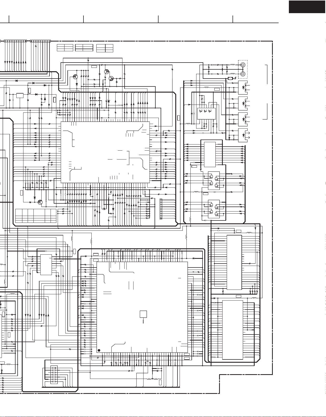
HT-R640
TO NAVD-8819
(SD-4:F1)
P2006A
8
9
7
5
6
10
SPRLSB
SPRLCS
SPRLF
SPRLZ2
SELY
SELV
D104
10K
S812C56AUA-C3G-T2
2
R105
104Z
470/16
+
C706
C701
VOLA
LEDZONE2
LEDSTBY
FLDSDO
FLDCLK
FLDCS
FLDRST
MICDET
MICMUT
VMRST
VMSTB
TXMUTE
RXMUTE
KEYINT1
KEYINT0
KEY3
KEY2
KEY1
KEY0
R172
47
47
R173
L302
LBC2518T4R7M
LBC2518T2R2M
L301
+
(VX)
470/6.3
(VX)
470/6.3
+
+3.3V
C301
R319
47
64
R318
47
63
R317
47
62
L313
61
R315
47
60
R314
47
59
58
57
56
+5.0V
55
47
R312
54
53
104Z
C314
52
C313
51
104Z
50
47
R338
49
L304
LBC2518T4R7M
+
(VX)
C304
470/6.3
330
OPT3
330
OPT1
330
OPT2
330
COAX1
330
COAX2
330
HDMISPF
330
OPTF
4
SYNC
1SS355
Q702
I
TYPE
D
P
W, G
+5VDSP
3
OSDCS
O
G
1
102K
C616-621
+5.0V
L313
LM182
TX
TO NADG-8817
(SD-7:G5)
1
123456789
2
0
OSDCLK
OSDSDO
XMDACRST
XMCOMSEL
XMREQERR
D703
1SS355
D701
1SS355
+5.6V
3
+
C702
100/16
102K
10K
R706
C615
2.7K
R719
C616
C617
C618
C619
D601
+
C604
Q601
4.7/50
RN1404
R618,R627,
R628,R649,
R616 R617
NO
YES
YESNONO
MCHSEL_3.3V
R181
330
330
R182
330
R183
R185
330
330
L182 LM182
R186
47
R184
DPSCLKIN
DIR_LRCK
OMCK
SAI_LRCK
DIR_SDOUT
JL101A
R101
XMSRRXD
XMSRTXD
XMSRSEL
1SS355
+5VMPU
R731
+
C704
DX-5R5L224
10K
R713
R716
R717
R718
R720
R722
2.7K
2.7K
R723
R721
C620
1SS355
R652
YESYES
NO
NO
C181
1
SELECT
2
1A
3
1B
4
1Y
5
2A
6
2B
7
2Y
8
GND93Y
TC74VHC157FT
CX_SDIN2
CX_SDIN3
R316
47
TRST
GNDXM
XMRST
D702
D705
1K
C705
27K
27K
10K
R698
R710
R701
R702
R703
R704
R705
R707
R708
R709
R711
R712
R714
R715
R725
C621
104Z
C603
R625 R626
220 NO
1K
104Z
VCC
Q181
CX_SDIN1
CX_LRCK
CX_SCLK
CX_SDIN4
JTAG
10
12
14 13
EMU0
+5VXM
1SS355
+
1K
4.7K
4.7K
4.7K
4.7K
4.7K
R724
4.7K
2.7K
ST
4A
4B
4Y
3A
3B
2
4
6
8
+5VCPU
100/16
R694
R692
R696
220
220
220
220
1K
220
220
220
47
220
10K
10K
YESNONO
16
15
14
13
12
11
10
+5.0V
330
TYPE
103
104
105
106
107
108
109
110
111
112
113
114
115
116
117
118
119
120
121
122
123
124
125
126
127
128
47K
R619
R602
R604
R606
330
R190
R193
47
R189
R188
DIR_BCK
SAI_SLCK
P711
1
3
5
7
9
11
DD
PP
+5VCPU
RI
VOLB
102K
1K
C614
R697
10K
102
P11/D9
P04/AN04/D4
P03/AN03/D3
P02/AN02/D2
P01/AN01/D1
P00/AN00/D0
P117
P116
P07/AN07/D7
P06/AN06/D6
P113
P112
P111
P110
P107/AN7/KI3
P106/AN6/KI2
P105/AN5/KI1
P104/AN4/KI0
P103/AN3
P102/AN2
P101/AN1
AVss
P100/AN0
1
104Z
C601
10K
10K
10K
330
47
R191
SAI_SDOUT
DEC_DSP_3.3V
NIC_DSP_3.3V
R262-
R269
330
EMU1
R101
YES
NONE
RN2402
Q602
SD
REMIN
HPDET
STEREO
220
1K
R690
R695
1K
1K
R693
R691
98
99
101
100
P14/D12
P13/D11
P12/D10
5
4
47
220
C602 104Z
R603 47
R601
R605
VMSDI
VMCLK
VMSDO
L181
DIGSDO_3.3V
DIGSDI_3.3V
PCMSBLR
PCMSLR
PCMCSW
SAI_SLCK
SAI_LRCK
CX_SCLK
RMCK
CX_LRCK
R290
10K
TDI
TCK
TDO
TMS
TYPE
JL101A
YES
DD
PP
NONE
R672
1M
10K
10K
10K
10K
R678
R679
R683
R685
R681
R682
D604
1SS355
R684
IRIN
INT1
INT2
INT3
BAND
SYSOUT
THERMAL
220
47K
220
R687
R689
97
P15/D13/INT3
P95/ANEX0/CLK4
6
R607 220
VCRST
R677
96
93
94
95
90
91
92
P17/D15/INT5
P16/D14/INT4
P20/AN20/A0(/D0/-)
P25/AN25/A5(/D5/D4)
P24/AN24/A4(/D4/D3)
P23/AN23/A3(/D3/D2)
P22/AN22/A2(/D2/D1)
P21/AN21/A1(/D1/D0)
P10/D8
P07/AN07/D7
P06/AN06/D6
P05/AN05/D5
Vref2Avcc3P97/_ADTRG/SIN4
P96/ANEX1/SOUT4
P94/DA1/TB4IN7P93/DA0/TB3IN8P92/TB2IN/SOUT3
P91/TB1IN/SIN310P90/TB0IN/CLK311P14112P14013BYTE14CNVss15P87/XCIN16P86/XCOUT17RESET18Xout19Vss20Xin21Vcc122P85/NMI23P84/INT224P83/INT125P82/INT026P81/TA4IN/U27P80/TA4OUT/U28P77/TA3IN29P76/TA3OUT30P75/TA2IN/W31P74/TA2OUT/W32P73/CTS2/RTS2/TA1IN/V
9
220
220
220
220
220
R615
R621
R610
R612
R609
R608
R613
1M
R617
10K
OSDCLK
OSDSDO
VMUT
SYNC
OSDCS
R678
TYPE
NO
DD
33K
PP
RN2402
R732
+5.0V
Q752
47
+
RN1404
Q751
C753
470/6.3
LIST
33K
10K
VOLH
SEC1H
C611
PROTECT
104Z
220
220
R674
C613
104Z
R675
R676
87
86
88
89
Vss
P30/A8(/-/D7)
P27/AN27/A7(/D7/D6)
P26/AN26/A6(/D6/D5)
Q701
MAIN MICRO PROCESSOR
10K
220
R618
6.000MHz
R616 1K
CNVSS
XMSRSEL
RDSDAT
RESET
R752
1K
R753
+
AMUT
C752
105K
TRGZ2
220K
C607
UDZS5.1B
D603
R686
220
104Z
220
C612
104Z
R673
85
80
Vcc2
P12481P12382P12283P12184P120
M30627FHPGP
P60/CTS0/RTS0
P62/RXD0/SCL0
P63/TXD0/SDA0
P64/CTS1/RTS1/CTS0/CLKS1
10K
R620
C605
104Z
220
C606
104Z
R623
X701
D602
1SS355
R622
10K
POFF
VSYNC
10K
R624
R625
1K:D-TYPE
220:PP
2.2K
1/50
C751
P61/CLK0
P65/CLK1
R625
220
R627
XMREQERR
XMCOMSEL
RDSCLK
R751
10K
VPOWER
APOWER
POFF2_5
220
220
R671
Vss
R631
220
220
220
R629
R628
XMDACRST
DSPCLK
DIRINT0
R632
220
DSPINT2
L201
DSPCS_3.3V
DSPCLK_3.3V
BLM21PG221SN1
+3.3V
470/6.3
R286
R253
R254
R255
R256
R257
R258
R259
C228
C210
47
C229
C271
10K
GPIO1
GPIO2
GPIO3
GPIO4
GPIO5
104Z
C215
R252
10K
104Z
R260
R261
R262
104Z
R263
R264
R265
R266
R267
R268
R269
C213
C214
+
330
47
47
47
47
47
330
47
BLM21PG221SN1
D1.2V
109
110
112
113
115
116
117
119
120
122
123
126
127
128
130
133
136
137
138
139
140
141
142
143
144
104Z
104Z
104Z
R207
RESET_3.3V
330
330
R250
+1.2V
R251
+3.3V
106
107
108
111
VSS
AXR0[0]
114
SPIO_SIMO
VSS
SPIO_SOMI/I2C0_SDA
AXR0[1]
DVDD
AXR0[2]
AXR0[3]
118
VSS
AXR0[4]
AXR0[5]/SPI1_SCS
121
AXR0[6]/SPI1_ENA]
AXR0[7]/SPI1_CLK
CVDD
124
VSS
125
DVDD
AXR0[8]/AXR1[5]/SPI1_SOMI
AXR0[9]/AXR1[4]/SPI1_SIMO
CVDD
129
VSS
AXR0[10]/AXR1[3]
131
AXR0[11]/AXR1[2]
132
CVDD
VSS
134
AXR0[12]/AXR1[1]
135
AXR0[13]/AXR1[0]
DVDD
AXR0[14]/AXR2[1]
AXR0[15]/AXR2[0]
ACLKR0
VSS
AFSR0
ACLKX0
AHCLKR0/AHCLKR1
AFSX0
1
3
330
RMCK
DSPINT_3.3V
104Z
104Z
SD_CS
OE
CS2
RAS
C209
C227
97
98
99
100
101
102
103
104
105
VSS
CVDD
DVDD
EM_OE
EM_RW
EM_RAS
EM_CS[0]
EM_CS[2]
SPIO_CLK/I2C0_SCL
TMS320D707E001RFP250
VSS2AHCLKX0/AHCLKX2
AMUTE04AMUTE15AHCLKX1
VSS7ACLKX18CVDD9ACLKR110DVDD11AFSX112AFSR113VSS14RESET15VSS16CVDD17CLKIN18VSS19TMS
6
330
R200
10K
R201
C201
C221
R202
R204
R205
R203
R206
330
10K
10K
10K
10K
104Z
104Z
BA0
96
EM_BA[0]
SPIO_SCS/I2C1_SCL
AMUT
SPRLZ2
SPRLSB
SPRLCS
SPRLF
VOLDAT
VOLCLK
47
220
220
220
220
R666
R664
R668
R667
R665
R66947R670
R634
220
DEC
69
P43/A1970P42/A1871P41/A1772P40/A1673P37/A1574P36/A1475P35/A1376P34/A1277P33/A1178P32/A1079P31/A09
P50/WRL/WR
P51/WRH/BHE
P47/CS366P46/CS267P45/CS168P44/CS0
P57/RDY/CLKOUT
P72/CLK2/TA1OUT/V
P71/RXD2/SCL2/TA0IN/TB5IN
P70/TXD2/SDA2/TA0OUT
34
35
33
R638
R640
R642
R636
47
47
C609
220
220
C608
R643
R641
R630
R633
R635
R637
R639
NIC
SDET
PLLSDA
PLLSCL
A0
A10
BA1
91
92
93
94
95
VSS
DVDD
EM_A[10]
EM_BA[1]
VSS
SPIO_ENA/I2C1_SDA
65
64
P125
63
P126
62
P127
61
60
59
P52/RD
58
P53/BCLK
57
P130
56
P131
55
P132
54
P133
53
P54/HLDA
52
P55/HOLD
51
P56/ALE
50
49
P134
48
P135
47
P136
46
P137
45
44
43
42
41
40
39
P67/TXD1/SDA137Vcc138P66/RXD1/SCL1
36
R645
104Z
C610
10K
R626
101J
101J
2.2K
2.2K
10K
10K
10K
10K
10K
87
88
90
CVDD
EM_A[2]89EM_A[1]
EM_A[0]
Q201
DSP
THERMALPAD
145
GNDDG
CVDD21TRST22OSCVSS23OSCIN24OSCOUT25OSCVDD26VSS27PLLHV28TDI29TDO30VSS31DVDD32EMU[0]33CVDD34EMU[1]35TCK36VSS
20
10K
10K
104Z
104Z
R208
R209
104Z
C202
101J
C203
C245
L241
ACF451832-333
TRST
TMS
R726
R650
R649
R648
R647
VSS
R652
86
R663
R660
R656
R727
85
EM_A[3]
104Z
C242
470/6.3
220
CVDD
C241
R662
10K
220
10K
220
220
220
220
47
47
R646
47
R644
47
RESET
9
CNVSS
8
FRXD
7
FCLK
6
+5VCPU
5
FBUSY
4
FTXD
3
TO FLASH WRITER
GNDDG
2
APOWER
1
P751A
+5VDSP
104Z
A5A4A3A2A1
C226
81
82
83
VSS
DVDD
EM_A[5]84EM_A[4]
C204
+
+3.3V
TDI
DIGSDO
DIGSDI
DIGCLK
MCHSEL
DSPRST
DSPCS
DIRRST
R651
OSDINY
OSDINV
DIRCS
XMRST
XMSRRXD
XMSRTXD
FBUSY
FCLK
FRXD
FTXD
A7
A6
79
EM_A[7]80EM_A[6]
TDO
10K
78
C222
104Z
10K
R771
10K
10K
104Z
C208
77
VSS
EMU0
+5.0V
A11A9A8
74
75
CVDD
EM_A[9]76EM_A[8]
EM_WE_DQM[1]
EM_WE_DQM[0]
C205
104Z
EMU1
TCK
OPT1
OPT2
OPT3
COAX1
LBC2518T470M
COAX2
C225
73
DVDD
VSS
EM_A[11]
EM_CKE
EM_CLK
VSS
DVDD
EM_D[8]
CVDD
EM_D[9]
EM_D[10]
VSS
EM_D[11]
DVDD
EM_D[12]
EM_D[13]
CVDD
EM_D[14]
EM_D[15]
VSS
CVDD
EM_D[0]
EM_D[1]
DVDD
EM_D[2]
EM_D[3]
VSS
EM_D[4]
EM_D[5]
CVDD
EM_D[6]
DVDD
EM_D[7]
VSS
EM_WE
EM_CAS
+3.3V
+1.2V
104Z
220/6.3
+
C139
C140
L134
TX
DIRCS_3.3V
DIRRST_3.3V
DSPCS_3.3V
RESET_3.3V
MCHSEL_3.3V
DIGCLK_3.3V
DIGSDO_3.3V
DSPCLK_3.3V
C151
104Z
+3.3V
DIRINT0
DIRINT_3.3V
DSPINT2
DSPINT_3.3V
BLM21PG221SN1
L152
+5LOGIC
RXMUTE
RXMUTE_3.3V
VMSTB
VMSTB_3.3V
L151
BLM21PG221SN1
L202
BLM21PG221SN1
C272
104Z
470/6.3
+
72
LL241
71
L203
70
69
68
67
DQM1
66
D8
65
64
D9
63
D10
62
61
D11
C224
60
59
D12
58
D13
57
56
D14
55
D15
54
C207
53
D0
52
51
D1
50
49
D2
D3
48
47
D4
46
D5
45
C206
44
D6
43
C223
42
41
D7
40
DQM0
39
38
37
C230
C231
C232
C230-232
104Z
R135
220K
R136
220K
L133
LBC2518T4R7M
080D
10K
C135
R137
1
VCC13IN612OUT611IN510OUT59IN48OUT4
14
10K
R138
C137
104K
11
Y8
12
Y7
13
Y6
14
Y5
15
Y4
16
Y3
17
Y2
18
Y1
19
_G2
20
VCC1_G1
TC74VHCT08AFT
10K
R280
8
9
10
11
12
13
14 1
+5.0V
TC74VHCT08AFT
8
9
10
11
12
13
14 1
C153
104Z
CKE
CLK
R221
47
104Z
104Z
104Z
104Z
WE
CAS
R133
10
104K
C133
C131
101J
C132
101J
C134
104K
R134
10
+5.0V
65432
7
GND
10K
C136
080D
C138
R139
10
GND
9
A8
8
A7
7
A6
6
A5
5
A4
4
A3
TC74VHC541FT
3
A2
2
A1
Q151
Q152
GND
VCC
C152
104Z
Q153
GND
VCC
C281
C282
BA1
CS2
OE
D0
D8
D1
D9
D2
D10
D3
D11
D4
D12
D5
D13
D6
D14
D7
D15
GPIO4
220/6.3
C283
+
C284
D0
D1
D2
D3
D4
D5
D6
D7
DQM0
WE
CAS
RAS
SD_CS
BA0
A10
A0
A1
A2
A3
C285
104Z
Q131
080D
R140
+
104Z
104Z
10
11
12
13
14
15
16
17
18
19
20
21
22
23
24
25
LBC2518T2R2M
LBC2518T2R2M
C146
103K
74HCU04F
220K
220/6.3
7
6
5
4
3
2
7
6
5
4
3
2
220/6.3
25
26
27
28
29
30
31
32
33
34
35
36
37
38
39
40
41
42
43
44
45
46
47
48
R285
1
VCC0
2
DQ0
3
DQ1
4
GNDQ1
5
DQ2
6
DQ3
7
VCCQ1
8
DQ4
9
DQ5
GNDQ2
DQ6
DQ7
VCCQ2
LDQM
_WE
_CAS
_RAS
_CS
A11
A10
A0
A1
A2
A3
VCC1
P131
L131
R131
75
R132
L132
75
103K
C147
47
R141
C141
104Z
R142
47
C142
104Z
R143
47
C143
104Z
R144
220
+
C145
C144
104Z
DIRCS
DIRRST
DSPCS
DSPRST
MCHSEL
DIGCLK
DIGSDO
DSPCLK
R279
10K
DEC
DEC_DSP_3.3V
NIC
NIC_DSP_3.3V
10K
R278
DIGSDI
DIGSDI_3.3V
VMSDI
VMSDI_3.3V
+3.3V
A0
CE#
GND
OE#
Q0
Q8
Q1
Q9
Q2
Q10
RY/BY#
Q3
Q11
VCC
RESET#
Q4
Q12
ES29LV400ET-70TG
Q5
Q13
Q6
Q14
Q282
Q7
Q15/A-1
GND
BYTE#
A161A15
10K
+3.3V
GNDQ4
VCCQ4
GNDQ3
VCCQ3
or IC42S16100
M12L16161A-7TG
Q281
COAX1
COAX2
GP1FAV51TKBF
U131
IN
VCC
OPT1
GND
GP1FAV51RKF5
U132
IN
VCC
GND
GP1FAV51RKF5
U133
IN
VCC
GND
GP1FAV51RKF5
U134
IN
VCC
GND
BLM21PG221SN1
L281
24
A0
A1
A1
23
A2
A2
22
A3
A3
21
A4
20
A4
A5
19
A5
A6
A6
18
A7
17
GPIO5
A17
16
NC
15
14
NC
13
NC
330
R287
12
WE
11
WE#
10
NC
9
NC
8
A7
A8
7
A8
A9
A9
6
A10
A10
5
A11
4
A11
A12
3
GPIO1
A13
GPIO2
2
A14
GPIO3
R281
R282 R283
50
GND2
49
D15
DQ15
D14
48
DQ14
47
46
D13
DQ13
45
D12
DQ12
44
43
D11
DQ11
42
D10
DQ10
41
40
D9
DQ9
39
D8
DQ8
C286
38
37
104Z
NC2
36
DQM1
UDQM
CLK
35
CLK
CKE
34
CKE
33
NC1
A9
32
A9
A8
31
A8
A7
30
A7
29
A6
A6
28
A5
A5
27
A4
A4
26
GND1
<Note>
SD-x:XY is short for Shcematic Diagram-x and
each socket's location, X=A to H, Y=1 to 5.
OPT2
OPT3
DIGITAL
OUT
RESET_3.3V
R284
L282
DIGITAL IN
FLASH ROM
4M Bit
Q282
10K
R281-284
L282
BLM21PG221SN1
SD RAM
16M bit
Q281
Page 25
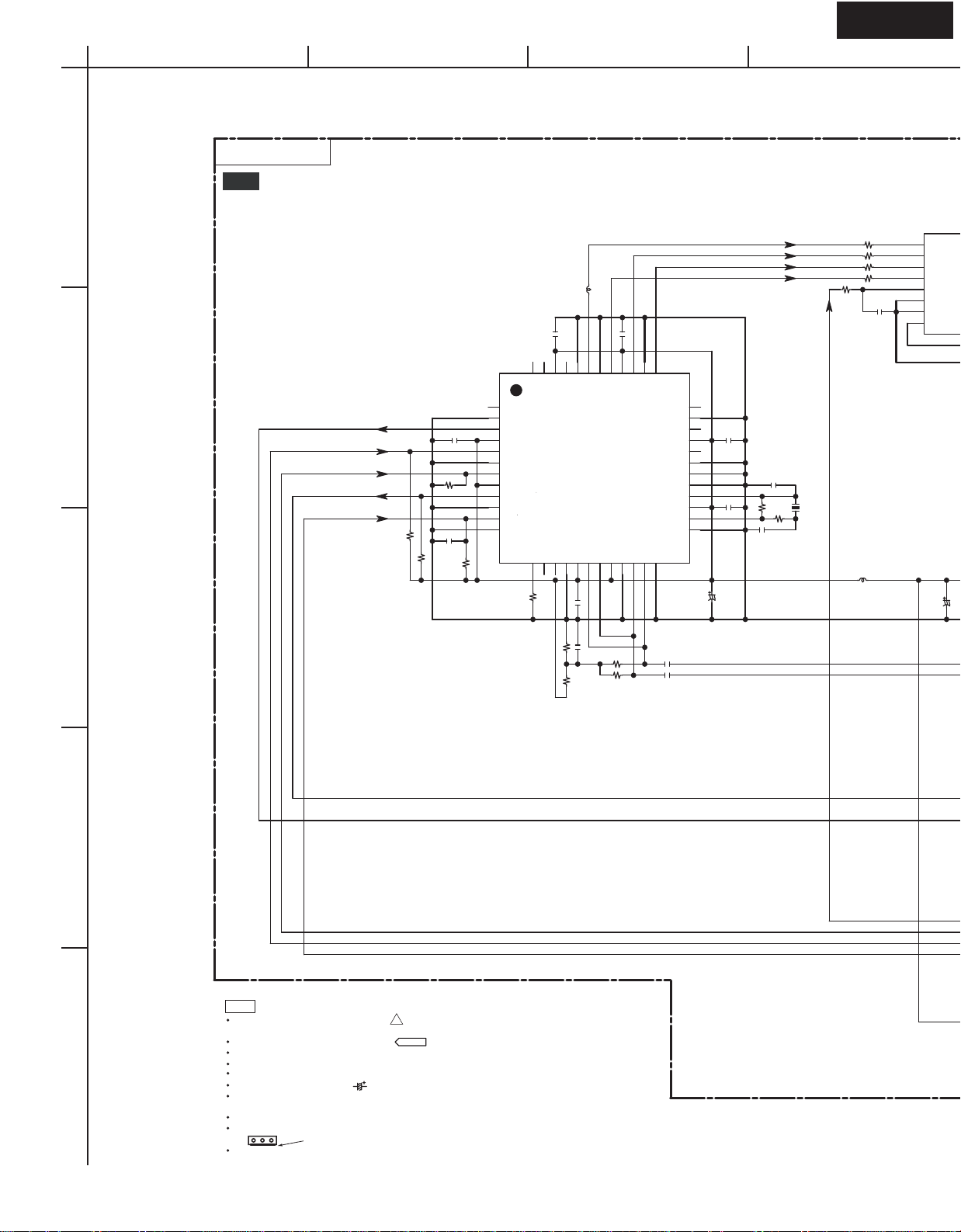
HT-R640
A
SCHEMATIC DIAGRAM-7
NADG-8817
1
2
3
U13
XM PC BOARD
XM_SDI_L
XM_SDO_L
XM_COM_SEL
XM_ERR_IRQ
XM_RESET
BCDEFGH
Q2002
AK4384ET
1
MCLK
2
BICK
3
SDTI
4
LRCK
5
PDN
6
SMUTE/CSN
7
ACKS/CCLK
8
DIF0/CDTI
+3.3V
C2033
TA48033AF
3
470/6.3
R2001
100K
R2003
100K
C2001
R2002
100K
C2002
102K
104Z
R2004
100K
1
LSDP
2
VSS
3
SC_TX_OUT
4
VDD
5
SC_RX_IN
6
VSS
7
CMD_SEL
8
VDD
9
ERR_IRQ
10
VSS
11
RST
12
SLAVE
_SEL
104Z
C2013
48
47
45
46
VDD
SAII_DA
SAII_EN
F2602E-01
COMM_RX_DIG
COMM_TX_DIG
COMM_TX_EN
13
14
15
16
100K
R2005
R2006
R2007
L2002
BK1608LM182
C2012
41
40
43
42
44
VSS
VSS
VDD
SAII_CLK
I2S_OCLK
I2S_LRCLK
Q2001
XMDTIC
VSS17VDD18COMM_RX_P
COMM_RX_M
VDD21VSS22COMM_TX_M
19
20
104Z
C2003
104Z
R2008
C2004
100
1K
R2009
1K
100
104Z
39
38
VSS
I2S_CLK
HSDP_CLK
COMM_TX_P
23
I2S_OCLK
I2S_SCLK
I2S_SDO
I2S_LRCLK
37
I2S_DA
HSDP_EN
VSS
VDD
HSDP_DA
VSS
TEST
VSS
OSC_IN
VDD
OSC_OUT
VSS
VSS
24
104Z
C2005
C2006
104Z
100
R2012
R2013
330
R2014
330
R2015
330
R2016
0
C2014
102K
DAC_RESET
36
35
34
C2011
33
104Z
32
31
30
29
28
27
26
25
C2007
C2010
104Z
100/16
C2009
080D
1M
R2011
R2010
C2008
040C
+3.3V_XM
X2001
45.1584MHz
680
L2001
LBC2518T2R2M
4
NOTE
THE COMPONENTS IDENTIFIED BY MARK ARE CRITICAL FOR SAFETY
REPLACE ONLY WITH PART NUMBER SPECIFIED.
VOLTAGE (MEASURED WITH VOLTMETER) IS DC VOLTAGE.(NO INPUT SIGNAL).
5
ALL PNP TRANSISTORS ARE EQUIVALENT TO 2SA1015-GR UNLESS OTHERWISE NOTED.
ALL NPN TRANSISTORS ARE EQUIVALENT TO 2SC1815-GR UNLESS OTHERWISE NOTED.
ALL DIODES ARE EQUIVALENT TO 1SS133 UNLESS OTHERWISE NOTED.
ELECTROLYTIC CAPACITORS ( ) ARE IN uF/WV.
ALL CAPACITORS ARE IN pF/50WV UNLESS OTHERWISE NOTED.
EX) 030- 3pF 330- 33pF 331- 330pF 333- 0.033uF
ALL RESISTORS ARE IN OHMS 1/4WATTS UNLESS OTHERWISE NOTED.
THE THICK LINES ON PC BOARD ARE THE PRINTING SIDE OF THE PARTS.
EX) PRINTING SIDE
CIRCUIT IS SUBJECT TO CHANGE FOR IMPROVEMENT.
!
Page 26
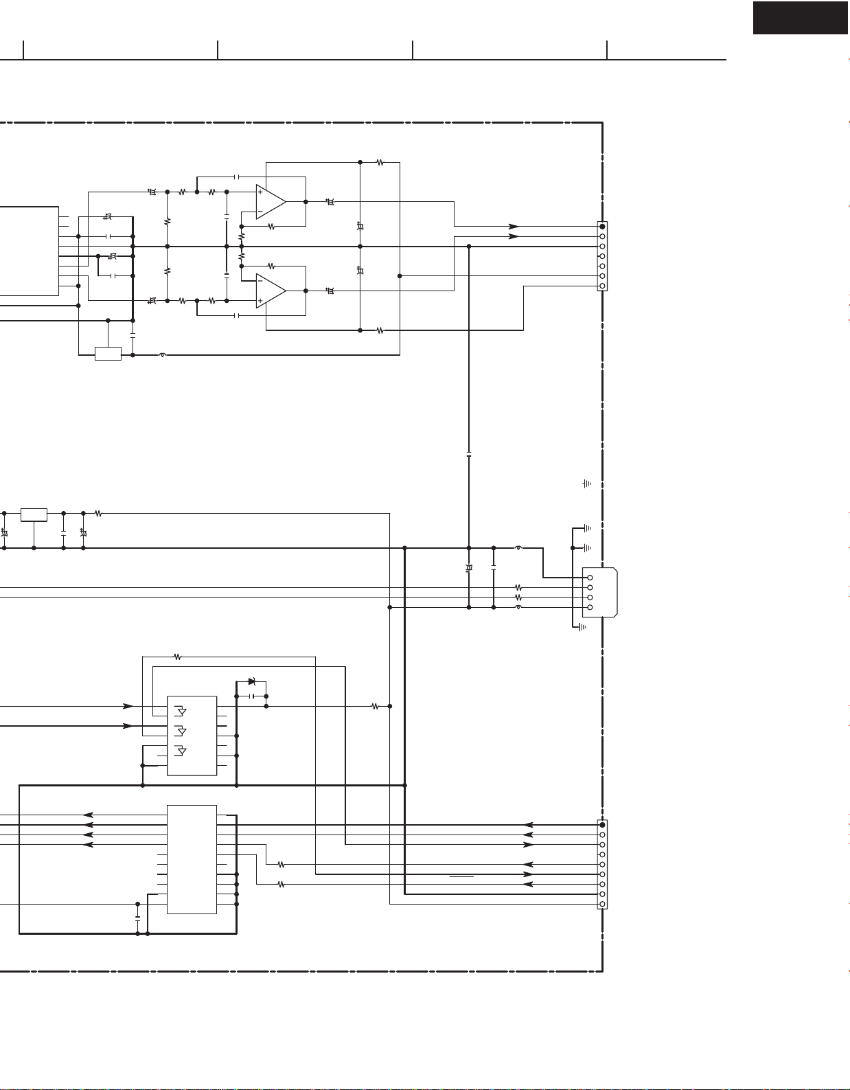
Q2002
DZFL
DZFR
VDD
VSS
2ch DAC
VCOM
AOUTL
AOUTR
P/S
16
15
14
13
12
11
10
9
+5V
1
C2018
470/6.3
C2017
104Z
C2016
10/50
C2015
104Z
2
O3I
Q2005
78L05
G
C2021
10/50
C2022
10/50
104Z
L2003
C2031
LBC2518T2R2M
R2023
R2024
R2021
2.2K
100K
100K
R2022
2.2K
R2025
2.2K
R2026
2.2K
C2025
821J
C2023
C2024
C2026
821J
821J
R2029
R2030
821J
3
2
3.3K
3.3K
6
5
NE5532APSR
8
Q2003
R2027
2.2K
R2028
2.2K
Q2003
4
NE5532APSR
HT-R640
R2031
22(1/2W)
C2027
1
10/50
C2029
220/16
C2030
C2028
7
10/50
220/16
R2032
22(1/2W)
XM_L_OUT
XM_R_OUT
GND_A
+12V
-12V
1
2
3
4
5
JL5502B
6
7
TO NAAF-8911 (SD-1:C1)
C2033
TA48033AF
3
470/6.3
Q2004
1
O
I
G
2
XM_ERR_IRQ
XM_SDI_L
DAC_RESET
XM_COM_SEL
XM_SDO_L
XM_RESET
C2032
104Z
R2047
22(1/2W)
C2043
100/16
R2036
0
Q2006
TC74HCT7007AF
1
2
3
4
5
6
7
GND8OUT4
Q2007
TC74VHC541FT
11
Y8
12
Y7
13
Y6
14
Y5
15
Y4
16
Y3
17
Y2
18
Y1
19
_G2
20
VCC1_G1
104Z
C2036
VCC
OUT6
OUT5
GND
102K
C2044
E2002
L2004
BLM21PG221SN1
104Z
C2042
C2034
100/16
R2033
22
R2034
22
L2005
BLM21PG221SN1
D2001
UDZS5.1B
C2035
104Z
14
13
IN6
12
11
IN5
10
9
IN4
10
9
A8
8
A7
7
A6
6
A5
5
A4
4
A3
3
A2
2
A1
R2035
R2046
0
0
R2044
220
XMDACRST
XMCOMSEL
XMERRIRQ
XMSRSEL
XMSRTXD
XMSRRXD
XMRST
GND
+5V_XM
E2003
E2001
4
3
2
1
P2001
GND
D+
XM
D-
+V
1
2
3
4
5
6
JL101B
7
8
9
TO NADG-8816 (SD-6:E1)
<Note>
SD-x:XY is short for Shcematic Diagram-x and
each socket's location, X=A to H, Y=1 to 5.
Page 27
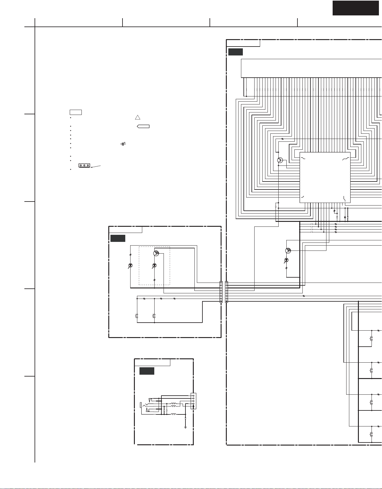
A
BCDEFGH
SCHEMATIC DIAGRAM-8(SD-8)
DISPLAY SECTION
1
NOTE
THE COMPONENTS IDENTIFIED BY MARK ARE CRITICAL FOR SAFETY
REPLACE ONLY WITH PART NUMBER SPECIFIED.
VOLTAGE (MEASURED WITH VOLTMETER) IS DC VOLTAGE.(NO INPUT SIGNAL).
ALL PNP TRANSISTORS ARE EQUIVALENT TO 2SA1015-GR UNLESS OTHERWISE NOTED.
ALL NPN TRANSISTORS ARE EQUIVALENT TO 2SC1815-GR UNLESS OTHERWISE NOTED.
ALL DIODES ARE EQUIVALENT TO 1SS133 UNLESS OTHERWISE NOTED.
ELECTROLYTIC CAPACITORS ( ) ARE IN uF/WV.
ALL CAPACITORS ARE IN pF/50WV UNLESS OTHERWISE NOTED.
EX) 030- 3pF 330- 33pF 331- 330pF 333- 0.033uF
2
3
4
ALL RESISTORS ARE IN OHMS 1/4WATTS UNLESS OTHERWISE NOTED.
THE THICK LINES ON PC BOARD ARE THE PRINTING SIDE OF THE PARTS.
EX) PRINTING SIDE
CIRCUIT IS SUBJECT TO CHANGE FOR IMPROVEMENT.
<Note>
SD-x:XY is short for Shcematic Diagram-x and
each socket's location, X=A to H, Y=1 to 5.
NADIS-8786
U02
SWITCH PC BOARD
2.2K
R7151
D7152
STBY
SLI-343URC
S7108
!
DTA114ES
STBY
R7104
820
Q7151
D7154
SDPB3DD0C
R7152
S7110
PURE AUDIO
120
R7105
1.2K
DD
PURE AUDIO
EXCEPT
PP ONLY
R7106
2.2K
LEDSTBY
GNDLED
+BLED
LEDPURE
KEY0_2
KEYINT0
NADIS-8785
U01
DISPLAY PC BOARD
F212F225P356P347P338P329P3110P3011P2912P2813P2714P2615P2516P2417P2318P2219P2120P2021P1922P1823P1724P1625P1526P1427P1328P1229P1130P1031P932P833P734P635P536P437P338P239P14016G4115G4214G4313G4412G4511G4610G479G488G497G506G515G524G
1
LEDSTBY
8
8
LEDZONE2
7
7
GNDCPU
6
6
+BLED
5
5
LEDPURE
4
4
KEY0_2
3
3
KEYINT0
2
2
1
1
JL7101A
JL7101B
C7001
223Z
R7001
100K
Q7004
2SC2458
Q7006
DTA114ES
D7001
VOLUME
SDPB3DD0C
R7010
Q7002
16-BT-128GNYK
49
SEG2
50
SEG1
51
SEG0
52
VCC2
53
DIG15/SEG39
54
DIG14/SEG38
55
DIG13/SEG37
56
DIG12/SEG36
57
DIG11
58
DIG10
59
DIG9
60
DIG8
61
DIG7
62
DIG6
63
DIG5
DIG4
64
DIG032DIG023DIG014DIG005_RESET6_CS7SCK8SDATA9P110P011VCC112XOUT13XIN14VSS15SEG35
1
104J
C7002
101J
C7003
C7004
101J
101J
C7005
120
R7103
560
42
SEG943SEG844SEG745SEG646SEG547SEG448SEG3
Q7003
M66005
3.3K
3.3K
R7006
220
220
33
32
SEG1834SEG1735SEG1636SEG1537SEG1438SEG1339SEG1240SEG1141SEG10
31
SEG20
SEG19
30
SEG21
29
SEG22
28
SEG23
27
SEG24
26
SEG25
25
SEG26
24
VP
23
SEG27
22
SEG28
21
SEG29
20
SEG30
19
SEG31
18
SEG32
SEG34
17
SEG33
16
+
100/6.3
104J
C7009
FLDRST
FLDCS
FLDCLK
FLDSDO
KEY0
+5V
S7102S7116
MULTIMEMORY
R7101
330
27K
101J
C7008
C7007
R7002
R7003
R7004
R7005
NAETC-8790
U06
KEY1
R7107
330
CD
TUNER
HEADPHONE
PC BOARD
P7201
5
4
2
HEADPHONES
5
3
7
8
1
102J
C7204
L7201
102J
C7203
022M
L7202
L7203
022M
022M
JL6605A
E7201
5
4
3
2
1
102J
C7201
KEY2
SD-5
TO NAVD-8819
KEY3
S7132
S7150
TUN UP
R7115
330
R7123
330
DIGITAL IN
PRESET UP
Page 28
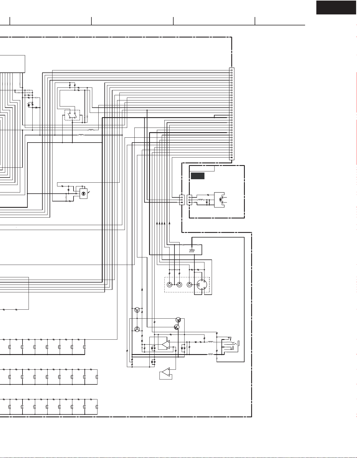
HT-R640
6G515G524G533G542G551G58F1159F12
223Z
C7010
R7007
220
C7011
223Z
R7008
220
C7012
223Z
223Z
C7014
C7013
33/50
D7002
MTZJ8.2C
C7015
100/16
+
R7021
10K
MASTER VOLUME
ROTARY
ENCODER
S7002
1
4
C7045
100/6.3
R7045
100
+
102K
C7047
R7046
1K
R7023
10K
R7022
10K
10K
R7024
3
103Z
103Z
5
2
C7022
C7021
L7032
022M
L7031
022M
+5.6V
5
4
3
2
1
U7042
REMOTE CONTROLLER
SENSOR
JL7351A
3
2
1
REMIN
FLDRST
FLDCS
FLDCLK
FLDSDO
KEY0
KEY1
KEY2
KEY3
+5.6S
KEYINT0
FAC1
KEYINT1
FAC2
-VP
VOLA
+5VDIS
VOLB
GNDCPU
V4_R
GNDV4
V4_L
LEDSTBY
V4V
GNDV4V
V4Y
LEDZONE2
V4C
GNDMIC
-12V
+12V
MICOUT
MICDET
MICMUT
OPTF
NAETC-8789
U05
FRONT OPT
PC BOARD
R7351
3
220
L7351
2
+
1
022M
JL7351B
C7352
100/16
C7351
IN
VCC
GND
TORX177L
223Z
36
35
34
33
32
31
30
29
28
27
26
25
24
23
22
21
20
19
18
17
16
15
14
13
TO NADG-8816 (SD-6)
12
11
10
9
8
7
6
5
4
3
2
1
P701B
U7351
VIDEO-4
DIGITAL
R7101
330
R7107
330
R7115
330
R7123
330
R7102
S7118
TUNER
S7134
DIGITAL IN
470
R7108
470
R7116
470
R7124
470
TAPE
S7120
S7136
DISPLAY
R7109
560
R7117
560
R7125
560
S7122
VIDEO4
S7138
LIS MODE>
R7110
820
R7118
820
R7126
820
S7124
VIDEO3
R7119
S7140
LIS MODE<
R7127
R7111
1.2K
1.2K
1.2K
S7126
VIDEO2
S7142
STEREO
R7112
2.2K
R7120
2.2K
R7128
2.2K
S7128
VIDEO1
S7144
TONE +
R7113
3.9K
R7121
3.9K
R7129
3.9K
DVD
S7130
S7146
TONE -
R7122
12K
R7130
12K
TONE
S7148
DTC114TS
DTC114TS
470
R7412
Q7404
R7414
Q7403
R7413
100K
10/16
220K
330J
C7405
C7404
R7410
R7409
+
220
220
MTZJ6.8B
33K
R7408
D7412
P7301
470
R7411
47/16
D7411
+
C7411
NJM4580D-D
+
C7412
NJM4580D-D
Q7401
MTZJ6.8C
C7301
471J
DTC114ES
R7406
7
47/16
1
R7301
Q7007
Q7401
4
8
C7303
104Z
C7302
471J
330
330
R7302
R L
VIDEO 4 INPUT
DTA114ES
Q7005
330
5
1K
6
+
R7407
D7401
MTZJ5.1B
3
2
R7303
47/16
C7403
75
101J
C7402
C7401
47K
R7405
10/16
C7304
104Z
E7301
R7304
+
75
R7404
220
R7403
L7401
L7402
022M
4.7K
022M
R7402
102J
R7401
47K
C7421
100
P7401
5
4
2
3
7
8
1
SETUP MIC
S7152
PRESET UP
S7154
ENTER
DOWN
PRESET
S7156
S7158
TUN DOWN
S7160
SETUP
S7162
RETURN
S7164
TUN MODE
S7166
DIMMER
RT/PTY/TP
Page 29
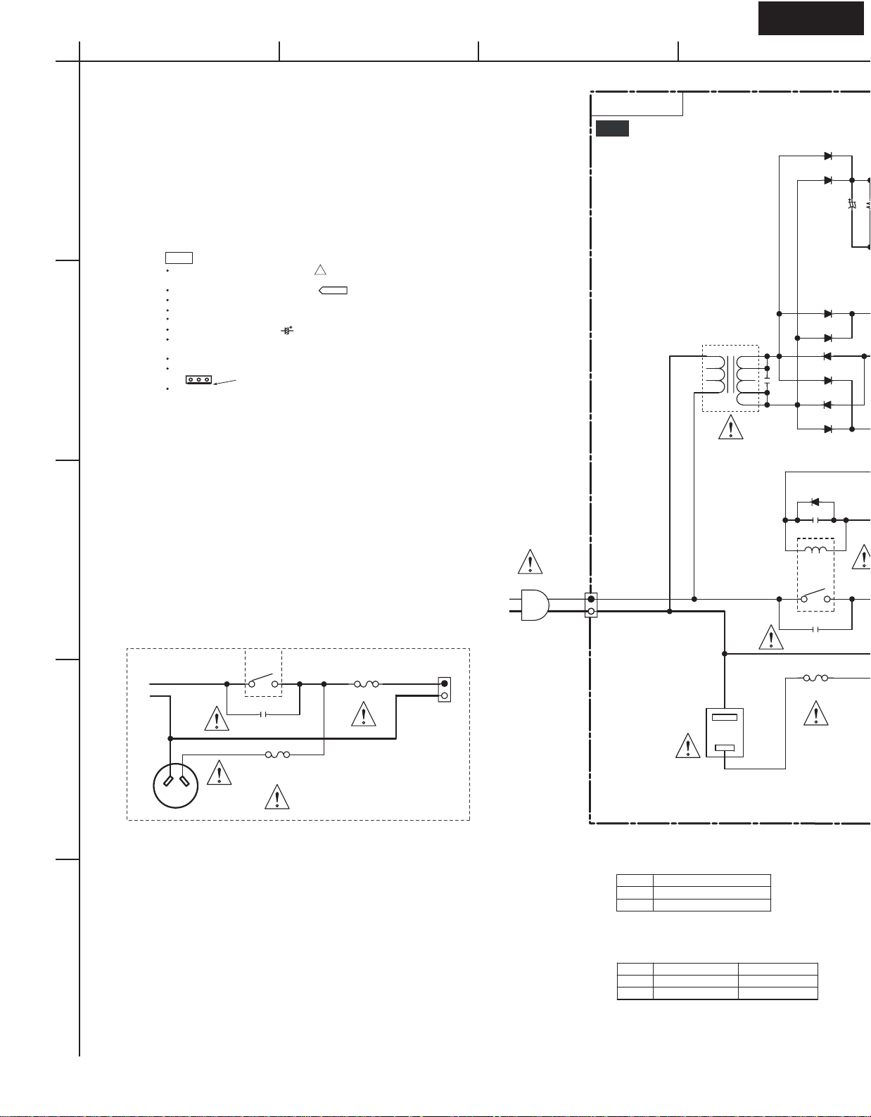
A
SCHEMATIC DIAGRAM-9(SD-9)
POWER SUPPLY SECTION
1
BCDEFGH
NAPS-8787
POWER SUPPLY PC BOARD
U03
D933
1SS133
D935
1SS133
C933
4.7/50
NOTE
THE COMPONENTS IDENTIFIED BY MARK ARE CRITICAL FOR SAFETY
REPLACE ONLY WITH PART NUMBER SPECIFIED.
VOLTAGE (MEASURED WITH VOLTMETER) IS DC VOLTAGE.(NO INPUT SIGNAL).
ALL PNP TRANSISTORS ARE EQUIVALENT TO 2SA1015-GR UNLESS OTHERWISE NOTED.
ALL NPN TRANSISTORS ARE EQUIVALENT TO 2SC1815-GR UNLESS OTHERWISE NOTED.
ALL DIODES ARE EQUIVALENT TO 1SS133 UNLESS OTHERWISE NOTED.
ELECTROLYTIC CAPACITORS ( ) ARE IN uF/WV.
ALL CAPACITORS ARE IN pF/50WV UNLESS OTHERWISE NOTED.
EX) 030- 3pF 330- 33pF 331- 330pF 333- 0.033uF
2
ALL RESISTORS ARE IN OHMS 1/4WATTS UNLESS OTHERWISE NOTED.
THE THICK LINES ON PC BOARD ARE THE PRINTING SIDE OF THE PARTS.
EX) PRINTING SIDE
CIRCUIT IS SUBJECT TO CHANGE FOR IMPROVEMENT.
<Note>
SD-x:XY is short for Shcematic Diagram-x and
each socket's location, X=A to H, Y=1 to 5.
!
D930
1SS133
T902
NPT-1519*
1
2
3
4
9
8
7
6
5
C921
223Z
3
1SS133
1SS133
1SS133
1SS133
1SS133
D925
1SS133
C902
104J
D931
D923
D921
D924
D922
56(1/2W)
2
3
PP
4 1
C901
103M/275VAC
RL901
F901
T5AL250V
AC CORD
1
2
P901A
1
2
P911
4 1
103M/275VAC
RL901
C901
F903
5A 125V
4
P902
AC OUTLET
100W MAX
F903
T2.5AL250V
P902
AC OUTLET
100W MAX
POWER SUPPLY VOLTAGE AND FREQ.
TYPE
D
120V 60HZ
PAC230-240V 50HZ
5
POWER TRANSFORMER
TYPE
D
P
T901
NPT-1518D
NPT-1518P
T902
NPT-1520JQ
NPT-1519GQ
Page 30
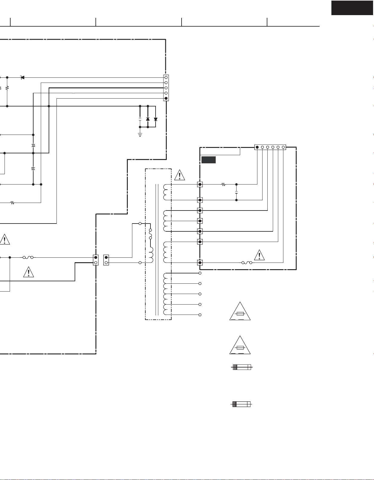
HT-R640
R934
R921
56(1/2W)
MTZJ5.1B
D934
100K
C922
2200/16
+
C930
100/35
+
POFF
+12VD
MPUGND
+10VS
POWERD
102J
C911
E901
D911
1SS133
5
4
3
2
1
D912
1SS133
POWER TRANS
T901
1
JL901A
(SD-5:A5)
TO NAVD-8819
S4
S3
NAETC-8788
U04
SEC TERMINAL-1
PC BOARD
R9102
8
5.6 (1/2W)
104J
9
10
11
12
13
C9101
TO NAVD-8819
(SD-5:A5)
12345
FLAC1
FLAC2
SEC3_2
SEC3_1
JL9101A
6
SEC2_1
SEC2_2
F901
10A 125V
1
2
1
2
3
S2
14
F910
5A 125V
P911
S1
CAUTION
(SD-2:A5)
TO NAPS-8912, P15-P19
FOR CONTINUED PROTECTION
AGAINST FIRE HAZARD, REPLACE
ONLY WITH FUSE OF SAME TYPE
AV
AND RATING INDICATED.
ATTENTION
CAUTIONF AFIN D'ASSURER UNE PROTECTION
V A
THIS SYMBOL LOCATED NEAR THE FUSE INDICATES
THAT THE FUSE USED IS SLOW OPERATING TYPE
FOR CONTINUED PROTECTION AGAINST FIRE FUSE
HAZARD,REPLACE WITH SAME TYPE FUSE. FOR FUSE
RATING REFER TO THE MAKING ADJACENT TO THE SYMBOL.
CE SYMBOLE INDIQUE QUE LE FUSIBLE UTLISE EST
A LENT, E POUR UNE PROTECTION PERMANENTE,N'UTILISER
QUE DES FUSIBLES DE MEME TYPE. CE DARNIER EST
INDIQUE LA QU LE PRESENT SYMBOL EST APPOSE.
PERMANENTE CONTRE LES RISQUES
D'INCENDIE, REMPLACER UNIQUEMENT
PAR UN FUSIBLE DE MEME TYPE
ET CALIBRATION COMME INDIQUE.
Page 31

HT-R640
A
SCHEMATIC DIAGRAM-10(SD-10)
HDMI SECTION
NAVD-8928
U21
1
2
3
4
5
HDMI PC BOARD
R1HPR
+3_3VHD1
1K
10K
R8534
R8545
R8541
R8538
10K
10K
22
HP DET
Shield
DDC DATA
DDC CLK
CERemote
CK Shield
D0 Shield
HDMI IN1
D1 Shield
P8501
D2 Shield
Shield
23
R2HPR
+3_3VHD1
Q8605
10K
1K
R8634
R8645
R8638
10K
22
HP DET
Shield
DDC DATA
DDC CLK
CERemote
CK Shield
D0 Shield
HDMI IN2
D1 Shield
P8601
D2 Shield
Shield
23
Q8510
Q8505
104Z
+5V
GND
CK-
CK+
D0+
D1+
D2+
104Z
R8641
10K
+5V
GND
CK-
CK+
D0+
D1+
D2+
R0PWR5V
10K
UM6K1N
R8536
D8501
C8599
102J
20
NC
D0-
D1-
D2-
C8598
21
Q8610
10K
UM6K1N
R8636
C8681
D8601
C8699
20
NC
D0-
D1-
D2-
C8698
21
3.3K
10K
R8535
C8581
19
18
17
16
15
14
13
12
11
10
9
8
7
6
5
4
3
2
1
10K
R8635
102J
19
18
17
16
15
14
13
12
11
10
9
8
7
6
5
4
3
2
1
102J
DTA144EE
3.3K
R8546
R8547
1SS226
102J
DTA144EE
3.3K
R8646
R8647
3.3K
1SS226
Q8603
PRODDC1
Q8503
UM6K1N
CEC
R0XCN
R0XCP
R0X0P
R0X0N
R0X1N
R0X1P
R0X2N
R0X2P
PRODDC2
UM6K1N
R1XCN
R1XCP
R1X0N
R1X0P
R1X1N
0
Q8504
8
7
WP
VCC
A02A13A24GND
1
0
8
7
WP
VCC
A02A13A24GND
1
CEC
R1X1P
R1X2N
R1X2P
SCLDDC1
SDADDC1
R8539
UM6K1N
R8542
5
6
SCL
SDA
DSCL0
DSDA0
R1PWR5V
SCLDDC2
SDADDC2
R8639
Q8604
R8642
UM6K1N
R8643
3.3K
6
5
SCL
SDA
DSCL1
DSDA1
R8540
3.3K
R8543
3.3K
R8640
3.3K
BCDEFGH
CEC
0
Q8506
256*8 EEPROM
BR24L02FV-W
0
Q8606
BR24L02FV-W
256*8 EEPROM
TO NAVD-8819 (SD-5:G3)
JL8001B
123
4
GND
+12DG
+12DG
GNDS2
+3.3V
+12.0V
22/4
C8517 105Z
C8518
C8519
102J
PVCC
C8520
22/4
C8521
37
PVCC0
102J
38
C8522
102J
102J
C8523
C8524
105Z
C8525
102J
102J
102J
C8528
102J
C8529
105Z
C8530
102J
C8531
102J
C8532
105Z
C8624
220/4
C8623
4
VOUT
VIN2VSS3CE
C8622
105Z
105Z
NC
1K
AVCC
39
R0XC-
40
R0XC+
41
AGND
42
AVCC
43
R0X0-
44
R0X0+
45
AGND
46
AVCC
47
R0X1-
48
R0X1+
49
AGND
50
AVCC
51
R0X2-
52
R0X2+
53
AGND
54
TMDSPGND
55
PVCC1
56
RSVD_A
57
AVCC
58
R1XC-
59
R1XC+
60
AGND
61
AVCC
62
R1X0-
63
R1X0+
64
AGND
65
AVCC
66
R1X1-
67
R1X1+
68
AGND
69
AVCC
70
R1X2-
71
R1X2+
72
AGND
R8567
0
R8568
0
R8569
0
R8570
0
R8571
0
R8572
0
R8573
0
R8574
0
C8526
C8527
R8575
0
R8576
0
R8577
0
R8578
0
R8579
0
R8580
0
R8581
0
R8582
0
L8506
BLM21PG221
+3_3VPLL
5
Q8602
1
XC6213B332M
R8633
+5VHD
L8591
BLM21PG221SN1
R0PWR5V
R1PWR5V
102J
C8516
34
35
33
36
CGND
CVCC18
R0PWR5V
+
C8585
DSCL0
DSDA0
32
31
DSCL0
DSDA0
R1PWR5V
470/16
DSCL1
30
DSCL1
223Z
C8586
DSDA1
29
DSDA1
1
5
104Z
C8587
SCL_RX
SDA_RX
28
27
CSCL
CSDA
VIN
SS
102J
C8515
26
IOVCC
Q8593
SI-8008
GND
3
105Z
C8514
25
24
CGND
IOGND
SW
VADJ
23
CVCC18
22
2
4
102J
C8513
20
21
CGND
VPP3318
L8592
NCH-2541 470K
CRS09
D8591
18
19
17
DL2
DL3
DR3
DR2
C8511
16
IOVCC
Q8501
SII9033
HDMI Receiver
CGND74CVCC1875IOGND76IOVCC77MUTEOUT78SPDIF79CVCC1880CGND81SD382SD283SD184SD085WS86SCK87NC88MCLKOUT89IOVCC90IOGND91CGND92CVCC1893NC94AUDPVCC18
105Z
C8533
73
102J
C8534
102J
C8535
33
33
R8509
R8508
MUTERX
HDMISPF
102J
C8536
PCMSBLR
33X4
R8511
PCMCSW
PCMSLR
33
R8512
PCMLR
PCMLRCK
33
R8513
BK1608LL241
PCMBCK
105Z
C8538
C8537
102J
L8517
47
R8514
MCK_HDMI
C8539
102J
28.332MHz
C8540105Z
+3_3VHD1
+5.0V
4.7K
R8591
R8592
820
R8593
105Z
12
14
13
15
DL0
DL1
DR1
IOGND
AUDPGND96XTALOUT97XTALIN98XTALVCC99REGVCC
95
C8541
102J
070D
R8516
C8543
C8542
33
X8501
R8515
1M
TO NAVD-8816, P801A (SD-6:D3)
181716151413121110
VD_SI
VDRST
VD_SCK
TXMUTE
+
47K
C8588
470/16
HDM_VSYNC
33
102J
105Z
R8503
C8505
EVNODD
RSVDL
102
100
R8518
C8547
102J
RST_RX
6
NC7NC8NC
RESET#
SCDT
103
4.7K
R8517
100
R8519
SCDT
C8504
4
5
IOVCC
INT
104
105
105Z
R8520
INT_RX
3
IOGND
VSYNC
CVCC18
CGND
106
C8548
100
11
070D
DR0
C8544
10
105Z
9
DCLK
100NC101
C8545
102J
C8546
105Z
VD_SO
VD_STB
RXMUTE
HDM_BLNK
HDM_HSYNC
DVCC
33
33
R8502
R8501
2
1
DE
ePAD
HSYNC
Q0
Q1
Q2
Q3
Q4
CVCC18
CGND
Q5
Q6
IOGND
IOVCC
Q7
Q8
Q9
Q10
Q11
CVCC18
CGND
Q12
Q13
Q14
Q15
IOVCC
ODCK
IOGND
Q16
Q17
Q18
Q19
CGND
CVCC18
Q20
Q21
Q22
Q23
IOVCC
CLK48B
IOGND
107
108
R8521
C8549
C8589
10K
102J
22/4
987
GND
HDMISPF
145
144
143
142
141
140
139
138
137
136
135
134
133
132
131
130
129
128
127
126
125
124
123
122
121
120
119
118
117
116
115
114
113
112
111
110
109
22/4
C8550
GND
C8502
C8501
R8528
C8561
C8560
C8559
R8526
C8558
R8525
R8524
C8556
R8523
C8555
R8522
C8554
C8553
C8552
22/4
22/4
102J
105Z
33
PCMLR
22/4
IOVCC
C8551
Page 32

432
PCMCSW
PCMSLR
+5VHD
C8591
105Z
1
I
2
G
Q8591
O
3
100/4
C8592
+3_3VHD1
L8501
L8502
L8504
L8505
BLM21PG221
CVCC18
HDM_CB2
HDM_CB3
HDM_CB4
HDM_CB5
C8562
105Z
R8527
33X4
HDM_Y2
HDM_Y3
HDM_Y4
HDM_Y5
HDM_Y6
HDM_Y7
HDM_Y8
HDM_Y9
HDM_CR2
HDM_CR3
HDM_CR4
HDM_CR5
HDM_CR6
HDM_CR7
HDM_CR8
HDM_CR9
BLM21PG221
L8508
L8507
BLM21PG221
L8509
BLM21PG221
P8003B
1
PCMSBLR
MCK_HDMI
C8593
1
G
Q8592
BA18BCOFP
3
100/4
C8594
105Z
I
2
O
+1_8VHD2
C8595
105Z
I
G
Q8595
O
BA18BCOFP
C8596
100/4
+1_8VHD3
+3_3VHD1
FOR NAVD8824
C8428 050C
HDM_Y6
HDM_Y5
HDM_Y4
HDM_Y3
HDM_PIXCLK
HDM_Y2
HDM_CB9
HDM_CB8
HDM_CB7
HDM_CB6
HDM_CB5
HDM_CB4
HDM_CB3
HDM_CB2
HDM_BLNK
1
2
3
100K
100K
HDM_CB6
HDM_CB7
HDM_CB8
HDM_CB9
C8424
C8425
C8426
+1.8V
R8739-R8742
R8746-R8756
22
DVDA_ENH
RXMUTE
INT_VSYNC
RTC
HDMI_POW
DVIHDMI
TEST0
RST_RX
R1HPR
R2HPR
VDOFF
RST_IP
HPD_TX
HDOE
RST_VE
RST_VD
R8757
R8758
R8421
22X4
100D
R8422
22
22X4
105Z
102J
105Z
C8427
102J
22
R8424
22X4
BLM21PG221
BLM21PG221
+1_8VHD3
+3_3VHD1
L8701
C8708
C8428
R8423
R8424
R8425
R8426
105Z
22
22/4
C8401
R8738
R8739
R8756
R8755
R8754
R8740
R8741
R8752
R8747
R8748
R8749
R8750
R8751
R8742
R8753
R8744
22
220M
C8423
61
62
63
64
65
66
67
68
69
70
71
72
73
74
75
76
77
78
79
80
81
PROEP2
PROEP1
PRODDC1
PRODDC2
22X4
R8737
DB0
DB1
DB2
DB3
71
72
73
74
75
76
77
47K
PDL5/FLMD1
78
PDL6/AD6
79
PDL7/AD7
PDL8/AD8
80
PDL9/AD9
81
PDL10/AD10
82
22
PDL11/AD11
83
PDL12/AD12
84
PDL13/AD13
85
PDL14/AD14
86
PDL15/AD15
87
PDH0/A16
88
PDH1/A17
89
P711/ANI11
90
P710/ANI10
91
P79/ANI9
92
P78/ANI8
93
P77/ANI7
94
P76/ANI6
95
P75/ANI5
96
P74/ANI4
97
P73/ANI3
98
P72/ANI2
99
P71/ANI1
100
P70/ANI0
R8746
AVREF0
220/4
C8709
4.7K
R8704
HDM_Y7
105Z
C8422
22x4
102J
R8418
59
60
CGND
D13
D12
D11
D10
D9
IDCK
D8
D7
D6
D5
IOVCC
IOGND
CGND
CVCC18
D4
D3
D2
D1
D0
DE
ePAD
HSYNC2VSYNC3CGND4CVCC185SPDIF6MCLK7SD38SD29SD110SD011WS12SCK13IOVCC14IOGND15CGND16CVCC1817INT18HPD19DSDA20DSCL
1
22/4
22
C8403
C8402
105Z
L8401
R8401
L8402
HDM_HSYNC
PDL0/AD0
PDL1/AD1
PDL2/AD2
PDL3/AD3
PDL4/AD4
AVSS03 P10/ANO04 P11/ANO15 AVREF16 PDH4/A207 PDH5/A218 FLMD09 VDD0
1
2
105Z
C8701
C8702
MODE1
MODE0
4.7K
R8702
R8417
22X4
HDM_Y8
HDM_Y9
HDM_CR3
HDM_CR2
HDM_CR4
CVCC18
HDMI Transmitter
22
22
22
C8404
102J
R8404
R8402
R8403
HDM_VSYNC
HDMISPF
MCK_HDMI
PCMSBLR
R8712-8715
R8729-8732
R8736,R8761
105Z
C8707
70
66
65
68
67
69
BVSS
BVDD
PCT4/_RD
PCT6/ASTB
PCT1/_WR1
MPD70F3716GC-8EA
REGC
10
11
105Z
C8704
4.7/50
C8703105Z
R8706
10K
X8701
CSTCR5M00G53-B0
R8416
22X4
HDM_CR7
HDM_CR6
HDM_CR5
HDM_CR9
HDM_CR8
49
D2350D2251D2152D2053D1954D1855D1756D1657D1558D14
Q8401
SII9030
22
22X4
R8406
R8405
R8407
PCMBCK
PCMLR
PCMLRCK
PCMSLR
PCMCSW
22
63
64
62
PCT0/_WRO
PCM2/_HLDAK
PCM3/_HLDRQ
Q8701
VSS0
12 X113 X214
C8705
X8701
105Z
VDRST
C8419
102J
105Z
C8421
C8420
48
47
46
CGND
IOVCC
IOGND
22
105Z
102J
C8406
C8405
HS
INT_VD
TXMUTE
R8732
R8736
58
59
60
61
PHD3/A19
PDH12/A18
PCM0/_WAIT
PCM1/CLKOUT
RESET
XT1
XT2
P02/NMI
15
16
17
18
R8720
R8707
R8719
22
22
10K
D8701
INT_TX
RST_TX
1SS355
SDA_TX
4.7k
4.7k
SCL_TX
102J
R8415
R8414
44
45
42
43
CSCL
CSDA
RESET#
CVCC18
EXT_SWING
22
22
102J
R8409
R8408
C8407
INT_TX
SDAODDC
HPD_TX
MUTERX
HPLGDET
R8730
R8731
57
56
P913/INTP4
P914/INTP5
P915/INTP6
P04/INTP0
P04/INTP1
P05/INTP2/_
19
20
R8721
R8710
22
10K
INT_RX
RST_TX
7k
105Z
4.7k
4.
R8411
R8413
41
CI2CA
NC
PGND2
PVCC2
AGND
TX2+
TX2-
AVCC
TX1+
TX1-
AGND
TX0+
TX0-
AVCC
TXC+
TXC-
AGND
PVCC1
PGND1
RSVDL
BLM21PG221
1SS226
SCLODDC
FSI
FSO
FCLK
R8715
R8714
R8713
53
55
54
P910/SIB3
P911/SOB3
P912/_SCKB3
P90/SDA02
P38/SDA00
P32/ASCKA0
P31/RXDA0
P06/INTP3
PP40/SDA01
P41/SCL01
21
22
23
22
R8709
SCDT
SCLODDC
SDAODDC
XC6213B332M
+5VHD
C8451
1K
R8452
BLM21PG221
C8418
40
C8417
39
C8416
38
C8415
37
102J
36
35
34
33
32
C8414
31
105Z
30
29
28
27
C8413
26
C8412
25
R8410
24
23
22
C8411
21
R8427
C8410
C8409
C8408
D8301
R8325
VD_SO
VD_SCK
R8729
R8761
51
52
P98/SOB1
P99/SCKB1
P97/SIB1
P96/A6
P95/A5
P94/A4
P93/A3
P92/A2
P91/SCL02
P55/DMS
P54/DCK
P53/DDO
P52/DDI
P51
P50
P39/SCL00
EVDD
EVSS
P37
P36
P35
P34
P33
P42
P30TXDA0
24
25
2.2K
R8712
Q8404
1
VIN
2
VSS
3
CE4NC
22/4
105Z
102J
102J
105Z
560
4.7K
105Z
22/4
22/4
L8403
Q8306
4.7K
1
R8324
2
3
47K
VD_SI
R8762
50
49
48
22
R8705
47
2.2K
46
R8727
45
44
43
R8726
42
2.2K
41
40
39
38
R8734
37
36
35
C8706
34
105Z
33
32
R8725
31
30
29
28
27
R8759
26
2.2K
R8760
2.2K
2.2K
R8711
R8716
R8717
R8718
5
VOUT
C8452
L8404
L8405
R8462
BLM21PG221
CEC_IO
CEC
SCLODDC
102J
R8337
SDAODDC
R8338
DVIHDMI
R8333
1K
+3_3VHD1
TC7SZ08FU
INA
VCC
INB
GND4OUTY
22
2.2K
R8733
2.2K
2.2K
R8724
R8723
R8722
22
0
0
220/4
C8453
105Z
27K
DLP2ADN900HL4L
DLP2ADN900HL4L
UM6K1N
4.7K
4.7K
5
HPLGDET
CEC_IO
VD_STB
SCL_TX
SDA_TX
SCLDDC2
SDADDC2
OC_DMS
OC_DCK
OC_DDO
OC_DDI
2.2K
2.2K
2.2K
OC_FLMDO
OC_SYSRST
+3_3VHD1
L8407
1
2
3
4 5
L8406
1
2
3
4 5
D8461
Q8309
Q8308
DTA144EE
R8334
2.2K
R8335
2.2K
C8330
105Z
C8329
105Z
SCL_VDVE
SDA_VDVE
SCLDDC1
SDADDC1
SCL_RX
SDA_RX
SCL_IP
SDA_IP
TX2+
8
TX2-
7
TX1+
6
TX1TX0+
8
TX0-
7
TXC+
6
TXC-
1SS226
C8332
105Z
22/16
C8328
C8327
R8728
DBGRXD
+3.3VMPU
DBGTXD
GND
105Z
C8461
C8398
102J
1
2
3
4
5
6
7
8
9
10
11
12
13
14
15
16
17
18
19
C8399
TX_HPLG
102J
4
VO
BYP2GND1CONT
3
105Z
R8323
10KX4
D2+
D2 Shield
D2D1+
D1 Shield
D1D0+
D0 Shield
D0CK+
CK Shield
CKCERemote
NC
DDC CLK
DDC DATA
GND
+5V
HP DET
5
VIN
10K
FWFLMD0
+3.3VMPU
FWRESET
2
4
6
8
10
12
14
16
18
20 19
1
2
3
4
5
6
7
8
9
0
R8708
23
21
Shield
Shield
20
22
100
R8341
105Z
C8326
Q8305
NJM2860F3-05
HDMI_POW
FCLK
FSO
FSI
C8710
(P8703)
P8302
HS
105Z
(P8704)
+12DG
8
7
6
5
4
3
2
1
P8702
1
3
5
7
9
11
13
15
17
Debug
HT-R640
FLASH MICOM WRITER
HDMI OUT
+5.0V
<Note>
SD-x:XY is short for Shcematic Diagram-x and
each socket's location, X=A to H, Y=1 to 5.
Page 33

HT-R640
A
SCHEMATIC DIAGRAM-11
DIGITAL AUDIO WAVE FORM SECTION
NOTE:
1.
WF01 is short for WaveForm01 .
1
2
2. See SD-6(SCHEMATIC DIAGRAM-6) for details.
74HCU04F
Q131
COAX1
4
COAX1
COAX2
DIGITAL
OUT
OPT1
OPT2
OPT3
1
R336
COAX2
10
13
R337
IN
VCC
GND
IN
R141
VCC
WF01
GND
IN
R142
VCC
GND
IN
R143
VCC
GND
TX
6
9
OPT1
OPT2
OPT3
WF02
43
42
50
46
45
48
Q301
DIR
TO NAVD-8928 (SD-10)
WF03
SAI_SDOUT
54
R312
SAI_SLCK
61
R316
SAI_LRCK
60
R315
WF04
CS42518-CQ
LR CLOCK (SAI_LRCK, CX_LRCK)
Fs=48kHz : DVD, Clock width=20.8us
Fs=44.1kHz : CD, Clock width=22.7us
BCD
P801A
1
3
2
PCMSLR
MCK_HDMI
PCMSBLR
WF05
4
PCMCSW
7
5
6
PCMLR
PCMBCK
PCMLRCK
14
12
13
11
9
10
5
7
6
Q181
TC74VHC157FT
TMS320D707E001
Q201
DSP
113
138
137
115
135
SAI_SDOUT
SAI_SLCK
SAI_LRCK
MASTER CLOCK=128Fs or 256Fs
116
117
120
139
142
141
144
BIT CLOCK (SAI_SLCK, CX_SLCK)
64Fs=3072kHz : DVD, Clock width=325ns
64Fs=2822.4kHz : CD, Clock width=354ns
CX_SDIN1
CX_SDIN2
CX_SDIN3
CX_SDIN4
CX_SCLK
CX_LRCK
WF07
WF06
WF08
R254
R255
R256
R257
R267
R269
1
DAC
64
63
62
2
3
WF09
R411
DAC_OUT DAC_OUT+
33
32
30
31
37
36
29
28
26
27
23
22
20
21
34
35
R401
R412
R402
R413
R403
R415
R405
R416
R406
R417
R407
R418
R408
R414
R404
Q401
Q401
Q402
Q403
Q403
Q404
Q404
Q402
FL
FR
C
SL
SR
SBL
SBR
SW
WF10
AUDIO_FL
WF01
OPT1
4.0V
WF02
COAX1
5.0V
WF03
SAI_SDOUT
3.3V
3
Duty varies according to audio data
SAI_LRCK
WF04
3.3V
4
WF07
20.8us
CX_LRCK
3.3V
20.8us
Duty always varies according to audio data
SAI_SLCK
WF05
325 ns
WF08
CX_SCLK
325 ns
3.3V
3.3V
Duty varies according to audio data
CX_SDIN1
WF06
20.8us
WF09
DAC_OUT-
Analog audio wave form with aliasing noise
3.3V
2.8V
0V
AUDIO_FL
WF10
WF10
AUDIO_FL
5
2.8V
Analog audio wave form with aliasing noise
0V
Aliasing noise in no audio data
220mVp-p
Page 34

HT-R640
A
PRINTED CIRCUIT BOARD VIEWS-1
U01
1
2
DISPLAY PC BOARD
(NADIS-8785)
Component Side
BCD
3
4
5
Page 35

HT-R640
Page 36

HT-R640
A
PRINTED CIRCUIT BOARD VIEWS-2
U01
1
2
DISPLAY PC BOARD
(NADIS-8785)
Soldering Side
BCD
3
4
5
Page 37

HT-R640
Page 38

HT-R640
A
PRINTED CIRCUIT BOARD VIEWS-3
U02
1
2
SWITCH PC BOARD
(NADIS-8786)
Component Side
BCD
3
Soldering Side
4
5
Page 39

HT-R640
A
PRINTED CIRCUIT BOARD VIEWS-4
U03
1
2
POWER SUPPLY PC BOARD
(NAPS-8787)
Component Side
BCD
3
U04
SEC. TERMINAL-1 PC BOARD
(NAETC-8788)
Component Side
Soldering Side
4
5
Page 40

HT-R640
A
PRINTED CIRCUIT BOARD VIEWS-5
U05
1
2
U06
FRONT OPT PC BOARD
(NAETC-8789)
Component Side
HEADPHONE JACK PC BOARD
(NAETC-8790)
BCDEFGH
Component Side
3
4
U07
OUTLET TERMINAL PC BOARD
(NAETC-8793)
Component Side
5
Page 41

HT-R640
U08
PRI. SWITCH PC BOARD
(NASW-8794)
Component Side
Page 42

HT-R640
A
PRINTED CIRCUIT BOARD VIEWS-6
U12
1
2
DSP PC BOARD
(NADG-8816)
Component Side
BCDEFGH
3
4
5
Page 43

HT-R640
Page 44

HT-R640
A
PRINTED CIRCUIT BOARD VIEWS-7
U12
1
2
DSP PC BOARD
(NADG-8816)
Soldering Side
BCDEFGH
3
4
5
Page 45

HT-R640
Page 46

HT-R640
A
PRINTED CIRCUIT BOARD VIEWS-8
U13
1
2
XM PC BOARD
(NADG-8817)
Component Side
BCD
3
Soldering Side
4
5
Page 47

HT-R640
A
PRINTED CIRCUIT BOARD VIEWS-9
U14
1
2
VIDEO PC BOARD
(NAVD-8819)
Component Side
BCD
3
4
5
Page 48

HT-R640
Page 49

HT-R640
A
BCD
PRINTED CIRCUIT BOARD VIEWS-10
U14
1
2
VIDEO PC BOARD
(NAVD-8819)
Soldering Side
3
4
5
Page 50

HT-R640
Page 51

HT-R640
A
BCD
PRINTED CIRCUIT BOARD VIEWS-11
U15
1
2
AMPLIFIER PC BOARD
(NAAF-8911)
Component Side
3
4
5
Page 52

HT-R640
Page 53

HT-R640
A
BCD
PRINTED CIRCUIT BOARD VIEWS-12
U15
1
2
AMPLIFIER PC BOARD
(NAAF-8911)
Soldering Side
3
4
5
Page 54

HT-R640
Page 55

HT-R640
A
BCD
PRINTED CIRCUIT BOARD VIEWS-13
U16
1
2
SEC. TERMINAL-2 PC BOARD
(NAPS-8912)
Component Side Soldering Side
3
U17
4
5
THERMAL SENSOR PC BOARD
(NAETC-8913)
Component Side
Page 56

HT-R640
A
BCD
PRINTED CIRCUIT BOARD VIEWS-14
U19
1
2
DRIVER AMPLIFIER PC BOARD
(NAAF-8917)
Component Side
3
U20
4
5
SPEAKER TERMINAL PC BOARD
(NAETC-8918)
Component Side
Page 57

HT-R640
Page 58

HT-R640
A
PRINTED CIRCUIT BOARD VIEWS-15
U21
1
2
HDMI PC BOARD
(NAVD-8928)
Component Side
BCDEFGH
3
4
5
Page 59

Soldering Side
HT-R640
Page 60

IC BLOCK DIAGRAMS AND TERMINAL DESCRIPTIONS -1
Q4003: ADV7172 (Digital PAL/NTSC Video Encoder with six DACs)
BLOCK DIAGRAM
HT-R640
MD-2000
FIELD/
TTX
TTXREQ
V
AA
P0
COLOR
DATA
P7
PAL
CLOCK
INSERTION BLOCK
4:2:2 TO
4:4:4
INTER-
POLATOR
NTSC
TELETEXT
8
8
8
VIDEO TIMING
GENERATOR
Y
YCrCb
U
TO
YUV
MATRIX
V
8
8
8
CLAMP
SCLOCK SDATA
I2C MPU PORT
BRIGHTNESS AND
CONTRAST CONTROL
SATURATION CONTROL
+
ADD SYNC
+
INTERPOLATOR
+
ADD BURST
+
INTERPOLATOR
CONTROL CIRCUIT
REAL-TIME
SCRESET/RTC
ALSB
PROGRAMMABLE
10
SHARPNESS
10
PROGRAMMABLE
10
LUMA
FILTER
+
FILTER
CHROMA
FILTER
GND
YUV TO
RBG
MATRIX
+
YUV
LEVEL
CONTROL
BLOCK
MODULATOR
+
HUE
CONTROL
10 10
SIN/COS
DDS BLOCK
M
10
10
U
10-BIT
L
DAC
T
10
10
I
10-BIT
P
DAC
L
E
10
10
10-BIT
X
DAC
E
R
DAC
CONTROL
M
BLOCK
U
L
10
10-BIT
T
I
P
L
E
X
E
R
10
10-BIT
10
10-BIT
DAC
CONTROL
BLOCK
DAC
DAC
DAC
10
10
10
DAC A
DAC B
DAC C
V
REF
R
SET2
COMP2
DAC E
DAC F
DAC D
R
SET1
COMP1
PIN CONFIGURATION
V
AA
P0
P1
P2
P3
P4
P5
P6
P7
CSO_HSO
V
AA
GND
AA
RESET
VSO
CLOCK
GND
48 47 46 45 44 39 38 3743 42 41 40
1
PIN 1
2
IDENTIFIER
3
4
5
6
7
8
9
10
11
12
13 14 15 16 17 18 19 20 21 22 23 24
GND
HSYNC
V
ADV7172
TOP VIEW
BLANK
ALSB
PAL NTSC
GND
CLAMP
TTX
AA
V
SCLOCK
FIELD/VSYNC
SET1
R
SCRESET/RTC
TTXREQ
SET2
R
SDATA
COMP2
REF
V
DAC F
36
35
34
33
32
31
30
29
28
27
26
25
COMP1
DAC A
V
AA
DAC B
V
AA
GND
V
AA
DAC C
DAC D
V
AA
GND
DAC E
Page 61

MD-2000
HT-R640
IC BLOCK DIAGRAMS AND TERMINAL DESCRIPTIONS -2
Q4003: ADV7172 (Digital PAL/NTSC Video Encoder with six DACs)
TERMINAL DESCRIPTION
Mnemonic Input/Output Function
P7–P0 I 8-Bit 4:2:2 Multiplexed YCrCb Pixel Port (P7ÐP0) P0 represents the LSB.
CLOCK I TTL Clock Input. Requires a stable 27 MHz reference clock for standard operation. Alter-
natively, a 24.5454 MHz (NTSC) or 29.5 MHz (PAL) can be used for square pixel operation.
HSYNC
FIELD/VSYNC I/O Dual Function FIELD (Mode 1) and
BLANK
SCRESET/RTC I This pin can be configured as an input by setting MR42 and MR41 of Mode Register 4. It
V
REF
R
SET1
R
SET2
COMP1 O Compensation Pin for DACs A, B, and C. Connect a 0.1 uF Capacitor from COMP to
COMP2 O Compensation Pin for DACs D, E, and F. Co nnect a 0.1 uF Capacitor from COMP to V
DAC A O GREEN/Composite/Y Analog Output. This DAC is capable of providing 34.66 mA output.
DAC B O BLUE/S-Video Y/U Analog Output. This DAC is capable of providing 34.66 mA output.
DAC C O RED/S-Video C/V Analog Output. This DAC is capable of providing 34.66 mA output.
DAC D O GREEN/Composite/Y Analog Output. This DAC is capable of providing 8.66 mA output.
DAC E O BLUE/S-Video Y/U Analog Output. This DAC is capable of providing 8.66 mA output.
DAC F O RED/S-Video C/V Analog Output. This DAC is capable of providing 8.66 mA output.
SCLOCK I MPU Port Serial Interface Clock Input.
SDATA I/O MPU Port Serial Data Input/Output.
CLAMP O TTL Output Signal to external circuitry to enable clamping of all video signals.
PAL_NTSC I Input signal to select PAL or NTSC mode of operation, pin set to Logic "1" selects PAL.
VSO
CSO_HSO
ALSB I TTL Address Input. This signal sets up the LSB of the MPU address.
RESET
TTX I Teletext Data Input Pin.
TTXREQ O Teletext Data Request output signal used to control teletext data transfer.
V
AA
GND
I/O
I/O Video Blanking Control Signal. The pixel inputs are ignored when this is Logic Level "0."
I/O Voltage Reference Input for DACs or Voltage Reference Output (1.235 V).
I A 150 resistor connected from this pin to GND is used to control full-scale amplitudes of
I A 600 resistor connected from this pin to GND is used to control full-scale amplitudes of
O VSO TTL Output Sync Signal.
O Dual Function
I T he input resets the on-chip timing generator and sets the ADV7172/ADV7173 into
P Power Supply (3 V to 5 V).
G
HSYNC
Mode) or as an input and accept (Slave Mode) Sync signals.
configured to output (Master Mode) or as an input (Slave Mode) and accept these
control signals.
This signal is optional.
can be configured as a subcarrier reset pin, in which case a low-to-high transition on this
pin will reset the subcarrier phase to Field 0. Alternatively it may be configured as a RealTime Control (RTC) Input.
the Video Signals from DACs A, B, and C (the "large" DACs).
the Video Signals from DACs D, E, and F (the "small" DACs).
V
COMP1 capacitor can be lowered to as low as 2.2 nF.
default mode. This is NTSC operation, Timing Slave Mode 0, DACs A, B, and C powered
OFF, DACs D, E, and F powered ON, Composite and S-Video out.
Ground Pin.
(Modes 1 and 2) Control Signal. This pin may be configured to output (Master
VSYNC
. For Optimum Dynamic Performance in Low Power Mode, the value of the
AA
or HSO TTL Output Sync Signal.
CSO
(Mode 2) Control Signal. This pin may be
AA
.
Page 62

IC BLOCK DIAGRAM AND TERMINAL DESCRIPTIONS -3
Q4001: ADV7183
(Advanced Video Decoder with 10-Bit ADC and Component Input Support)
HT-R640
BLOCK DIAGRAM
ADV7183
ISO
REFOUT
AIN1
AIN2
AIN3
AIN4
AIN5
AIN6
ANALOG I/P
MULTIPLEXING
AUTOMATIC
GAIN
CONTROL
(AGC)
CLAMP AND
DC RESTRE
PWRDN
SHAPING
AND
NOTCH LPF
10-BIT
ADC
27MHz
10-BIT
ADC
VIDEO TIMING AND
CONTROL BLOCK
HSYNC FIELD VSYNC HREF VREF CLOCK
LUMA
ANTIALIAS
LPF
SWITCH
PEAKING
HPF/LPF
SUB-
CARRIER
RECOVERY
DTO
CHROMA
ANTIALIAS
LPF
27MHz XTAL
OSCILLATOR
BLOCK
RESAMPLING
AND
HORIZONTAL
SCALING
SYNC
DETECTION
RESAMPLING
AND
HORIZONTAL
SCALING
SHAPING
LPF
CLOCK
LUMA
DELAY
BLOCK
2H LINE
MEMORY
CHROMA
COMB
FILTER
I2C-COMPATIBLE
INTERFACE PORT
SCLOCKRESET ALSB
SDATA
P15-P0
PIXEL
O/P PORT
FIFO CONTROL
BLOCK
AND
PIXEL
OUTPUT
FORMATTER
LLC
SYNTHESIS
WITH LINE-
LOCKED
OUTPUT
CLOCK
AFF
HFF/QCLK
AEF
DV
RD
OE
GL/CLKIN
LLC1
LLC2
LLCREF
ELPF
PIN CONFIGURATION
1
VS
2
HS
DGND
3
DVDDIO
DVDDIO
P11
P10
P9
P8
DGND
DVDD
NC
SFL
NC
DGND
NC
NC
NC
P7
P6
4
5
6
7
8
9
10
11
12
13
14
15
16
17
18
19
20
FIELD80OE79NC78NC77P1676P1775P1874P1973DVDD72DGND71NC70NC69SCLK68SDA67ALSB66NC65RESET64NC63AIN662AIN12
61
ADV7183A
TOP VIEW
24NC25
P521P422P323P2
27
28
LLC226LLC1
29
30
31P132P033NC34NC35
XTAL
DVDD
XTAL1
DGND
36
37
38
40
ELPF
PVDD
PWRDN
AGND39AGND
60
59
58
57
56
55
54
53
52
51
50
49
48
47
46
45
44
43
42
41
AIN5
AIN11
AIN4
AIN10
AGND
CAP C2
CAP C1
AGND
CML
REFOUT
AVDD
CAP Y2
CAP Y1
AGND
AIN3
AIN9
AIN2
AIN8
AIN1
AIN7
Page 63

HT-R640
IC BLOCK DIAGRAM AND TERMINAL DESCRIPTIONS -4
Q4001: ADV7183
(Advanced Video Decoder with 10-Bit ADC and Component Input Support)
TERMINAL DESCRIPTION (1/2)
Pin Mnemonic Input/Output Function
1 VS/VACTIVE O VS or Vertical Sync. A dual-function pin, (OM_SEL[1:0] = 0, 0) is an
output signal that indicates a vertical sync with respect to the YUV pixel
data. The active period of this signal is six lines of video long. The polarity
of the VS signal is controlled by the PVS bit. VACTIVE (OM_SEL[1:0] =
1, 0 or 0, 1) is an output signal that is active during the active/viewable
period of a video field. The polarity of VACTIVE is controlled by PVS bit.
2 HS/HACTIVE O
3, 14 DVSSIO G Digital I/O Ground
4, 15 DVDDIO P Digital I/O Supply Voltage (3.3 V)
5-8, 19-24, P15-P0 O Video Pixel Output Port. 8-bit multiplexed YCrCb pixel port (P15-P8),
32, 33, 73-76
9, 31, 71 DVSS1-3 G Ground for Digital Supply
10, 30, 72 DVDD1-3 P Digital Supply Voltage (3.3 V)
11 AFF O Almost Full Flag. A FIFO control signal indicating when the FIFO has
12 HFF/QCLK/GL I/O Half Full Flag. A multifunction pin, (OM_SEL[1:0] = 1, 0) is a FIFO
13 AEF O Almost Empty Flag. A FIFO control signal, it indicates when the FIFO
16 CLKIN I Asynchronous FIFO Clock. This asynchronous clock is used to output
17, 18, 34, 35 GPO[3:0] O General-Purpose Outputs controlled via I C
25 LLCREF O Clock Reference Output. This is a clock qualifier distributed by the inter-
26 LLC2 O Line-Locked Clock System Output Clock/2 (13.5 MHz)
27 LLC1/PCLK O Line-Locked Clock System Output Clock. A dual-function pin (27 MHz 5%)
28 XTAL1 O Second terminal for crystal oscillator; not connected if external clock
29 XTAL I Input terminal for 27MHz crystal oscillator or connection for external
36 PWRDN I Power-Down Enable. A logical low will place part in a power-down status.
37 ELPF I This pin is used for the External Loop Filter that is required for the LLC PLL.
38
39
PVDD
PVSS G
P
HS or Horizontal Sync. A dual-function pin, (OM_SEL[1:0] = 0, 0) is a
programmable horizontal sync output signal. The rising and falling edges
can be controlled by HSB[9:0] and HSE[9:0] in steps of 2 LLC1. The polarity
of the HS signal is controlled by the PHS bit. HACTIVE (OM_SEL[1:0]=
1, 0 or 0, 1) is an output signal that is active during the active/viewable
period of a video line. The active portion of a video line is programmable on
the ADV7183. The polarity of HACTIVE is controlled by PHS bit.
16-bit YCrCb pixel port (P15-P8 = Y and P7-P0 = Cb,Cr).
reached the almost full margin set by the user (use FFM[4:0]). The polarity
of this signal is controlled by the PFF bit.
control signal that indicates when the FIFO is half full. The QCLK
(OM_SEL[1:0] = 0, 1) pin function is a qualified pixel output clock when
using FIFO SCAPI mode. The GL (OM_SEL[1:0] = 0, 0) function
(Genlock output) is a signal that contains a serial stream of data that contains
information for locking the subcarrier frequency. The polarity of HFF signal
is controlled by PFF bit.
has reached the almost empty margin set by the user (use FFM[4:0]). The
polarity of this signal is controlled by PFF bit.
data onto the P19-P0 bus and other control signals.
2
nal CGC for a data rate of LLC2. The polarity of LLCREF is controlled
by the PLLCREF bit.
or a FIFO output clock ranging from 20 MHz to 35 MHz.
source is used.
oscillator with CMOS-compatible square wave clock signal
Page 64

IC BLOCK DIAGRAM AND TERMINAL DESCRIPTIONS -5
Q4001: ADV7183
(Advanced Video Decoder with 10-Bit ADC and Component Input Support)
TERMINAL DESCRIPTION (2/2)
Pin Mnemonic Input/Output Function
40, 47, 53, 56,
63
41, 43, 45, 57,
59, 61
42, 44, 46, 58,
60, 62
48, 49
50
51
52
54, 55
64
65
66
67
68
69
70
77
78
79
80
AVSS
AVSS1-6
AIN1-6
CAPY1-2
AVDD
REFOUT
CML
CAPC1-2
RESET
ISO
ALSB
SDATA
SCLK
VREF/VRESET
HREF/HRESET
RD
DV
OE
FIELD
G
G
I
I
P
O
O
I
I/O
I
I
I/O
I
O
O
I
O
I
O
Ground for Analog Supply
Analog Input Channels. Ground if single-ended mode is selected. These
pins should be connected directly to REFOUT when differential mode is
selected.
Video Analog Input Channels
ADC Capacitor Network
Analog Supply Voltage (5 V)
Internal Voltage Reference Output
Common-Mode Level for ADC
ADC Capacitor Network
System Reset Input. Active Low.
Input Switch Over. A low to high transition on this input indicates to the
decoder core that the input video source has been changed externally and
configures the decoder to reacquire the new timing information of the new
source. This is useful in applications where external video muxes are used.
This input gives the advantage of faster locking to the external muxed
video sources. A low to high transition triggers this input.
TTL Address Input. Selects the MPU address:
MPU address = 88h ALSB = 0, disables I C filter
MPU address = 8Ah ALSB = 1, enables I C filter
MPU Port Serial Data Input/Output
MPU Port Serial Interface Clock Input
VREF or Vertical Reference Output Signal. Indicates start of next field.
VRESET or Vertical Reset Output is a signal that indicates the beginning
of a new field. In SCAPI/CAPI mode this signal is one clock wide and
active low relative to CLKIN. It immediately follows the HRESET pixel,
and indicates that the next active pixel is the first active pixel of the next field.
HREF or Horizontal Reference Output Signal. A dual-function pin
(enabled when Line-Locked Interface is selected, OM_SEL[1:0] = 0,0),
this signal is used to indicate data on the YUV output. The positive slope
indicates the beginning of a new active line; HREF is always 720 Y samples
long. HRESET or Horizontal Reset Output (enabled when SCAPI or
CAPI is selected, OM_SEL[1:0] = 0, 1 or 1, 0) is a signal that indicates the
beginning of a new line of video. In SCAPI/CAPI this signal is one clock
cycle wide and is output relative to CLKIN. It immediately follows the last
active pixel of a line. The polarity is controlled via PHVR.
Asynchronous FIFO Read Enable Signal. A logical high on this pin enables
a read from the output of the FIFO.
DV or Data Valid Output Signal. In SCAPI/CAPI mode, DV performs to
functions, depending on whether SCAPI or CAPI is selected. It toggles
high when the FIFO has reached the AFF margin set by the user, and
remains high until the FIFO is empty. The alternative mode is where it can
be used to control FIFO reads for bursting information out of the FIFO. In
API mode DV indicates valid data in the FIFO, which includes both pixel
information and control codes. The polarity of this pin is controlled via PDV.
Output Enable Controls Pixel Port Outputs. A logic high will three-state
P19-P0.
ODD/EVEN Field Output Signal. An active state indicates that an even
field is being digitized. The polarity of this signal is controlled by the PF bit.
HT-R640
2
2
Page 65

K
K
IC BLOCK DIAGRAMS AND TERMINAL DESCRIPTIONS -6
Q2002: AK4384 (192kHz 24-Bit 2ch DAC )
HT-R640
BLOCK DIAGRAM
MCLK
Clock
Divider
Modulator
Modulator
SMUTE/CSN
ACKS/CCLK
DIF0/CDTI
LRC
BIC
SDTI
P/S
µP
Interface
Audio
Data
Interface
PDN
ATT
ATT
De-emphasis
Control
8X
Interpolator
8X
Interpolator
TERMINAL DESCRIPTION
No. Pin Name I/O Function
1 MCLK I Master Clock Input Pin
An external TTL clock should be input on this pin.
2 BICK I Audio Serial Data Clock Pin
3 SDTI I Audio Serial Data Input Pin
4 LRCK I L/R Clock Pin
5 PDN I Power -Down Mode Pin
When at “L”, the AK4384 is i n the power-down mode and is held in reset.
The AK4384 should always be reset upon power-up.
SMUTE I Soft Mute Pin in parallel mode
6
“H”: Enable, “L”: Disable
CSN I Chip Select Pin in serial mode
ACKS I Auto Setting Mode Pin in parallel mode
7
“L”: Manual Setting Mode, “H”: Auto Setting Mode
CCLK I Control Data Clock Pin in serial mode
DIF0 I Audio Data Interface Format Pin in parallel mode 8
CDTI I Control Data Input Pin in serial mode
9 P/S I
Parallel/Serial Select Pin (Internal pull-up pin)
“L”: Serial control mode, “H”: Parallel control mode
10 AOUTR O Rch Analog Output Pin
11 AOUTL O Lch Analog Output Pin
12 VCOM O Common Voltage Pin, VDD/2
Normally connected to VSS with a 0.1mF c
a 10m F electrolytic cap.
13 VSS - Ground Pin
14 VDD - Power Supply Pin
15 DZFR O Rch Data Zero Input Detect Pin
16 DZFL O Lch Data Zero Input Detect Pin
PIN CONFIGURATION
VDD
VSS
VCOM
DZFL
DZFR
SCF
LPF
SCF
LPF
AOUTL
AOUTR
MCLK
BICK
SDTI
LRCK
PDN
SMUTE/CSN
ACKS/CCLK
DIF0/CDTI
1
2
3
4
Top
View
5
6
7
8
eramic capacitor in parallel with
DZFL
16
DZFR
15
VDD
14
VSS
13
12
VCOM
AOUTL
11
AOUTR
10
P/S
9
Page 66

IC BLOCK DIAGRAM AND TERMINAL DESCRIPTIONS -7
Q4002: AN15881A (Video SW for TV with Multi-signal 14 Inputs and 4 Outputs)
BLOCK DIAGRAM
HT-R640
V1
V2
V3
V4
V5
V6
V7
V8
Y1
Y2
Y3
Y4
Y5
Y6
Y7
Y8
C1
C2
C3
C4
C5
C6
C7
C8
4/6dB
6dB
4/6dB
6dB
4/6dB
6dB
Buf
75<E
75<E
75<E
Buf
75<E
75<E
75<E
Buf
75<E
75<E
75<E
Vout1
Vout2
Vout2-FB
Vout3
Vout3-FB
Vout4
Vout4-FB
Yout1
Yout2
Yout2-FB
Yout3
Yout3-FB
Yout4
Yout4-FB
Cout4
Cout1
Cout2
Cout3
CY1
CY2
CY3
CY4
CY5
CY6
PB1
PB2
PB3
PB4
PB5
PB6
PR1
PR2
PR3
PR4
PR5
PR6
SDA
SCL
O1 O2
Logic
6dB
6dB
6dB
6dB
6dB
6dB
BIAS
75<E
75<E
75<E
75<E
75<E
75<E
VCC GNDMUTE
CYout2
CYout2-FB
CYout3
CYout3-FB
PBout1
PBout2
PRout1
PRout2
Page 67

IC BLOCK DIAGRAM AND TERMINAL DESCRIPTIONS -8
Q4002: AN15881A (Video SW for TV with Multi-signal 14 Inputs and 4 Outputs)
TERMINAL DESCRIPTION (1/3)
DescriptionTypePin namePin No.
Luminance signal in put 3InY31
Luminance signal input 4InY42
Luminance signal input 5InY53
Luminance signal input 6InY64
Luminance s ignal input 7InY75
Luminance signal in put 8InY86
5.0V power supplyPower supplyVCC17
Chrominance signal input 1InC18
Chrominance signal input 2InC29
Chrominance signal input 3InC310
Chrominance signal input 4InC411
Chrominance signal input 5InC512
GroundGroundGND113
Chrominance signal input 6InC614
Chrominance signal input 7InC715
Chrominance signal inpu t 8InC816
HT-R640
Bias voltageOutputBIAS17
CY1 signal inputInCY118
CY2 signal inputInCY219
CY3 signal inputInCY320
CY4 signal inputInCY421
CY5 signal inputInCY522
CY6 signal inputInCY623
PB1 signal inputInPB124
PB2 signal inputInPB225
PB3 signal inputInPB326
PB4 signal inputInPB427
PB5 signal inputInPB528
PB6 signal inputInPB629
PR1 signal inputInPR130
PR2 signal inputInPR231
PR3 signal inputInPR332
PR4 signal inputInPR433
PR5 signal inputInPR534
PR6 signal inputInPR635
Page 68

HT-R640
IC BLOCK DIAGRAM AND
TERMINAL DESCRIPTIONS -9
Q4002: AN15881A (Video SW for TV with Multi-signal 14 Inputs and 4 Outputs)
TERMINAL DESCRIPTION (2/3)
DescriptionTypePin namePin No.
Mute control pinInMUTE36
PROUT2 signal outputOutPROUT237
General output 1OutO138
PROUT1 signal outputOutPROUT139
General output 2OutO240
PBOUT2 signal outputOutPBOUT241
PBOUT1 signal outputOutPBOUT142
GroundGroundGND243
CYOUT3 feedback inputInCYOUT3-FB44
CYOUT3 signal outputOutCYOUT345
CYOUT2 feedback inputInCYOUT2-FB46
CYOUT2 signal outputOutCYOUT247
COUT4 signal outputOutCOUT448
5.0V power supplyPower supplyVCC249
COUT3 signal outputOutCOUT350
COUT2 signal outputOutCOUT251
COUT1 signal outputOutCOUT152
GroundGroundGND353
YOUT4 feedback inputInYOUT4-FB54
YOUT4 signal outputOutYOUT455
YOUT3 feedback inputInYOUT3-FB56
YOUT3 signal outputOutYOUT357
YOUT2 feedback inputInYOUT2-FB58
YOUT2 signal outputOutYOUT259
YOUT1 signal outputOutYOUT160
5.0V power supplyPower supplyVCC361
VOUT4 feedback inputInVOUT4-FB62
VOUT4 signal outputOutVOUT463
2
I
C bus data inputInSDA64
VOUT3 feedback inputInVOUT3-FB65
VOUT3 signal outputOutVOUT366
VOUT2 feedback inputInVOUT2-FB67
VOUT2 signal outputOutVOUT268
VOUT1 signal outputOutVOUT169
2
I
C bus clock inputInSCL70
Page 69

IC BLOCK DIA GRAM AND TERMINAL DESCRIPTIONS -10
Q4002: AN15881A (Video SW for TV with Multi-signal 14 Inputs and 4 Outputs)
TERMINAL DESCRIPTION (3/3)
DescriptionTypePin namePin No.
Video composite signal input 1InV171
Video composite signal input 2InV272
Video composite signal input 3InV373
Video composite signal input 4InV474
Video composite signal input 5InV575
Video composite signal input 6InV676
Video composite signal input 7InV777
Video composite signal input 8InV878
Luminance signal in put 1InY179
Luminance signal input 2InY280
HT-R640
PIN CONFIGURATION
SDA
64
VOUT3
VOUT2
VOUT1
SCL
65
66
67
68
69
70
71
V1
72
V2
73
V3
74
V4
75
V5
76
V6
77
V7
78
V8
79
Y1
80
Y2
1
Y3
VOUT3-FB
VOUT2-FB
VOUT4
63
2
Y4
VCC3
VOUT4-FB
626160
3
4
Y5
Y6
YOUT2
YOUT1
59585756555453
6
5
Y8
Y7
YOUT3
YOUT2-FB
789
C1
VCC1
YOUT3-FB
GND3
YOUT4
COUT1
YOUT4-FB
525150
AN15881A
10
C3C2C5
13
11
12
C4
GND1
CYOUT2-FB
CY2
CYOUT3-FB
CYOUT3
444342
212223
CY4
CY3C6CY5
PBOUT2
PBOUT1
41
40
O2
39
PROUT1
38
O1
37
PROUT2
36
MUTE
35
PR6
34
PR5
33
PR4
32
PR3
31
PR2
30
PR1
29
PB6
28
PB5
27
PB4
26
PB3
25
PB2
24
PB1
CY6
COUT4
VCC2
COUT3
COUT2
14
15
C7
CYOUT2
48
474645
49
17
181920
16
C8
CY1
BIAS
GND2
Page 70

IC BLOCK DIAGRAMS AND TERMINAL DESCRIPTIONS -11
Q8506,Q8606: BR24L02FV-W(256X8 bit EEPROM)
BLOCK DIAGRAM AND PIN CONFIGURATION
1
A0
2k Bit EEPROM Array
8
HT-R640
Vcc
8bit
A1
A2
2
3
Address
Decorder
Control circuit
GND
4
High-voltage
generation circuit
TERMINAL DESCRIPTION
Terminal
Vcc
I/O
-
Slave word
8bit
address register
START STOP
Power voltage
detection
Function
Apply a power source.
ACK
8bit
Data
register
7
WP
6
SCL
5
SDA
GND
A0,A1,A2
SCL
SDA
WP
-
I/O
Ground terminal
I
I
I
Slave address setting terminal
Serial clock input
Slave and word address.
Serial data input and output
Write protect terminal
Page 71

IC BLOCK DIAGRAMS AND TERMINAL DESCRIPTIONS -12
Q301 : CS42518 (8-Ch Codec with S/PDIF Receiver)
BLOCK DIAGRAM
HT-R640
RXP0
RXP1/GPO1
RXP2/GPO2
RXP3/GPO3
RXP4/GPO4
RXP5/GPO5
RXP6/GPO6
RXP7/GPO7
MUTEC
FILT+
VQ
REFGND
VA
AGND
AINL+
AINL-
AINR+
AINR-
AOUTA1+
AOUTA1-
AOUTB1+
AOUTB1-
AOUTA2+
AOUTA2-
AOUTB2+
AOUTB2-
AOUTA3+
AOUTA3-
AOUTB3+
AOUTB3-
AOUTA4+
AOUTA4-
AOUTB4+
AOUTB4-
TXP VARX AGND LPFLT DGND DGND VD
S/P DIF
Decoder
DEM
Gain & Chip
Gain & Chip
Digital Filter
Ref
Rx
GPO
MUTE
ADC#1
ADC#2
Analog Filter
Clock/Data
Recovery
Digital Filter
Digital Filter
DAC#1
DAC#2
DAC#3
DAC#4
DAC#5
DAC#6
DAC#7
DAC#8
C&U Bit
Data Buffer
Format
Detector
Internal MCLK
ADC
Serial
Data
VD
Mult/Div
Interface
Volume Control
Control
Port
Serial
Audio
Port
CODEC
Serial
Port
INT
RST
AD0/CS
AD1/CDIN
SDA/CDOUT
SCL/CCLK
VLC
OMCK
RMCK
SAI_LRCK
SAI_SCLK
SAI_SDOUT
VLS
ADCIN1
ADCIN2
CX_SDOUT
CX_LRCK
CX_SCLK
CX_SDIN1
CX_SDIN2
CX_SDIN3
CX_SDIN4
Page 72

IC BLOCK DIAGRAMS AND TERMINAL DESCRIPTIONS -13
Q301 : CS42518 (8-Ch Codec with S/PDIF Receiver)
PIN CONFIGURATION
CX_SDIN2
CX_SDIN3
CX_SDIN4
SAI_SCLK
SAI_LRCK
OMCK
ADCIN1
ADCIN2
CX_SDOUT
RMCK
SAI_SDOUT
VLS
CX_SDIN1
CX_SCLK
CX_LRCK
VD
DGND
VLC
SCL/CCLK
SDA/CDOUT
AD1/CDIN
AD0/CS
INT
RST
AINR-
AINR+
AINL+
AINL-
646362616059585756555453525150
1
2
3
4
5
6
7
8
9
10
11
12
13
14
15
16
CS42518
DGNDVDTXP
RXPO
49
48
47
46
45
44
43
42
41
40
39
38
37
36
35
34
33
RXP1/GP01
RXP1/GP01
RXP1/GP01
RXP1/GP01
RXP1/GP01
RXP1/GP01
RXP1/GP01
VARX
AGND
LPFLT
MUTEC
AOUTA1AOUTA1+
AOUTB1+
AOUTB1AOUTA2-
HT-R640
171819202122232425262728293031
VQ
FILT+
REFGND
AOUTB4-
AOUTB4+
VA
AOUTA4-
AOUTA4+
AGND
AOUTB3-
AOUTA3-
AOUTB3+
AOUTA3+
32
AOUTB2-
AOUTB2+
AOUTA2+
TERMINAL DESCRIPTION (1/3)
Pin Name # Pin Description
CX_SDIN1
CX_SDIN2
CX_SDIN3
CX_SDIN4
CX_SCLK CODEC Serial Clock (Input/Output) - Serial clock for the CODEC serial audio interface
CX_LRCK
VD
DGND
VLC
SCL/CCLK
SDA/CDOUT
AD1/CDIN
1
Codec Serial Audio Data Input (Input) - Input for two's complement serial audio data.
64
63
62
2
3
CODEC Left Right Clock (Input/ Output) - Determines which channel, Left or Right, is currently active on
the CODEC serial audio data line.
4
Digital Power (Input) - Positive power supply for the digital section.
51
5
Digital Ground (Input) - Ground reference. Should be connected to digital ground.
52
6
Control Port Power (Input) - Determines the required signal level for the control port.
7
Serial Control Port Clock (Input) - Serial clock for the serial control port. Requires an external pull-up
resistor to the logic interface voltage in I2C mode as shown in the Typical Connection Diagram.
8
Serial Control Data (Input/Output) - SDA is a data I/O line in IC mode and requires an external pull-up
resistor to the logic interface voltage, as shown in the Typical connection Diagram. CDOUT is the output
data line for the control port interface in SPI mode.
Address Bit 1 (I2C)/Serial Control Data (SPI) (Input) - AD1 a chip address pin in I2C mode; CDIN is
9
the input data line for control port interface in SPI mode.
Page 73

IC BLOCK DIAGRAMS AND TERMINAL DESCRIPTIONS -14
Q301 : CS42518 (8-Ch Codec with S/PDIF Receiver)
TERMINAL DESCRIPTION (2/3)
Pin Name # Pin Description
AD0/CS 10 Address Bit 0 (I2C)/Control Port Chip Select (SPI) (INput) - AD0 is a chip address pin in I2C mode; CS
is the chip select signal in SPI mode.
INT 11 Interrupt (Ountput) - The CS42518 will generate an interrupt condition as per the Interrupt Mask register.
RST 12 Reset (Input) - The device enters a low power mode and all internal registers are reset to their default
settings when low.
AINRAINR+
AINLAINL+
VQ 17 Quiescent Voltage (Output) - Filter connection for internal quiescent reference voltage.
FILT+ 18 Positive Voltage Reference (Output) - Positive reference voltage for the internal sampling circuits.
REFGND 19 Reference Ground (Input) - Ground reference for the internal sampling circuits.
AOUTA1 +, -
AOUTB1 +, AOUTA2 +, AOUTB2 +, AOUTA3 +, AOUTB3 +, AOUTA4 +, AOUTB4 +, -
VA
VARX
AGND 25
MUTEC 38 Mute Control (Output) - The Mute Control pin outputs high impedance following an initial power -on con-
LPFLT 39 PLL Loop Filer (Output) - An RC network should be connected between this pin and ground.
RXP7/GPO7
RXP6/GPO6
RXP5/GPO5
RXP4/GPO4
RXP3/GPO3
RXP2/GPO2
RXP1/GPO1
RXP0 49 S/PDIF Receiver Input (Input) - Dedicated receiver input for S/PDIF encoded data.
TXP 50 S/PDIF Transmitter Output (Output) - S/PDIF encoded data output, mapped directly from one of the
VLP 53 Serial Port Interface Power (Input) - Determines the required signal level for the serial port interfaces.
SAI_SDOUT 54
RMCK 55 Recovered Master Clock (Output) - Recovered master clock output from the External Clock Reference
13
14
15
16
36, 37
35, 34
32, 33
31, 30
28, 29
27, 26
22, 23
21, 20
24
41
40
42
43
44
45
46
47
48
Differential right Channel Analog Input (Input) - Signals are presented differentially to the delta-sigma
modulators via the AINR+/- pins.
Differential right Channel Analog Input (Input) - Signals are presented differentially to the delta-sigma
modulators via the AINR+/- pins.
Differential Analog Output (Output) - The full-scale differential analog output level is specified in the
Analog Characteristics specification table.
Analog Power (Input) - Positive power supply for the analog section.
Analog Ground (Input) - Ground reference. Should be connected to analog ground.
dition or whenever the PDN bit is set to a "1", forcing the codec into power -down mode. The signal will
remain in a high impedance state as long as the part is in power-down mode. The Mute Control pin goes
to the selected "active" state during reset, muting, or if the master clock to left/right clock frequency ratio
is incorrect. This pin is intended to be used as a control for external mute circuits to prevent the clicks
and pops that can occur in any single supply system. The use of external mute circuits are not mandatoy but may be desired for designs requiring the absolute minimum in extraneous clicks and pops.
S/PDIF Receiver Input/ General Purpose Output (Input/ Output) - Receiver inputs for S/PDIF encoded
data. The CS42518 has an internal 8:2 multiplexer to select the active receiver port, according to the
Receiver Mode Control 2 resister. These pins can also be configured as general purpose output pins,
ADC Overflow indicators or Mute Control outputs according to the RXP/General Purpose Pin Control
resisters.
receiver inputs as indicated by the Receiver Mode Control 2 resister.
Serial Audio Interface Serial Data Output (Output) - Output for two's complement serial audio PCM
data from the S/PDIF incoming stream. This pin can also be configured to transmit the output of the internal and external ADCs.
HT-R640
Page 74

IC BLOCK DIAGRAMS AND TERMINAL DESCRIPTIONS -15
Q301 : CS42518 (8-Ch Codec with S/PDIF Receiver)
TERMINAL DESCRIPTION (3/3)
Pin Name # Pin Description
CL_SDOUT 56 CODEC Serial Data Output (Output) - Output for two's complement serial audio data the internal
and external ADCs.
ADCIN1
ADCIN2
OMCK 59
SAI_LRCK 60
SAI_LRCK 61 Serial Audio Interface Serial Clock (Input/Output) - Serial clock for the Serial Audio Interface
58
57
External ADC Serial Input (Input) - The CS42518 provides for up two external stereo analog to digital
converter inputs to provide a maximum of six channels on serial data output line when the CS42518
is placed in One Line mode.
External Reference Clock (Input) - External clock reference that must be within the ranges specified in
currently active on the serial audio data line.
Serial Audio Interface Left/Right Clock (Input/Output) - Determines which channel, Left of Right, is
currently active on the serial audio data line.
HT-R640
Page 75

IC BLOCK DIAGRAMS AND TERMINAL DESCRIPTIONS -16
Q282 : ES29LV400 (4 Mbit Flash Memory)
BLOCK DIAGRAM
RY/BY
#
HT-R640
Vcc
Vss
WE
RESET#
A<0:17>
CE#
OE#
BYTE#
Vcc Dete
#
ctor
Command
r
Registe
Chip Enable
Output Enable
c
Logi
Timer/
Counter
Write
State
Machin
DQ0-DQ15(A-1
Analog Bias
Generato
e
Sector Swit
ches
r
Y-Decode
X-Deco
Address Latch
der
Input/Output
ers
Buff
Data Latch/
Sense Amp
r
Y-Decode
ll Array
Ce
)
s
r
Page 76

IC BLOCK DIAGRAMS AND TERMINAL DESCRIPTIONS -17
Q282 : ES29LV400 (4 Mbit Flash Memory)
PIN CONFIGURATION
HT-R640
A15
A14
A13
A12
A11
A10
A9
A8
NC
NC
WE#
RESET#
NC
NC
RY/BY#
NC
A17
A7
A6
A5
A4
A3
A2
A1
1
2
3
4
5
6
7
8
9
10
11
12
13
14
15
16
17
18
19
20
21
22
23
24
ES29LV400
48-Pin Standard TSOP
48
47
46
45
44
43
42
41
40
39
38
37
36
35
34
33
32
31
30
29
28
27
26
25
A16
BYTE#
Vss
DQ15/A-1
DQ7
DQ14
DQ6
DQ13
DQ5
DQ12
DQ4
Vcc
DQ11
DQ3
DQ10
DQ2
DQ9
DQ1
DQ8
DQ0
OE#
Vss
CE#
A0
TERMINAL DESCRIPTION
Terminal Description
A0-A17 18 Addresses
DQ0-DQ14 15 Data Input
DQ15/A-1
CE# Chip Enable
OE# Output Enable
WE# Write Enable
RESET# Hardware Reset Pin, Active Low
BYTE# Selects 8-bit or 16-bit mode
RY/BY# Ready/Busy Output
Vcc
Vss Device Ground
NC Pin Not Connected Inter
s/Outputs
DQ15 (Data Input/Output, Word Mode)
A-1 (LSB Address Input, Byte Mode)
3.0 volt-only single power supply
(see Product Selector Guide for speed options and voltage supply tolerances)
nally
Page 77

IC BLOCK DIAGRAMS AND TERMINAL DESCRIPTIONS -18
Q2001 : F2602E (XM Digital Transceiver)
BLOCK DIAGRAM
HT-R640
PIN CONFIGURATION
Page 78

IC BLOCK DIAGRAMS AND TERMINAL DESCRIPTIONS -19
Q2001 : F2602E (XM Digital Transceiver)
TERMINAL DESCRIPTION (1/2)
HT-R640
Page 79

IC BLOCK DIAGRAMS AND TERMINAL DESCRIPTIONS -20
Q2001 : F2602E (XM Digital Transceiver)
TERMINAL DESCRIPTION (2/2)
HT-R640
Page 80

IC BLOCK DIAGRAMS AND TERMINAL DESCRIPTIONS -21
Q281: IC42S16100 (16-Mbit Synchronous Dynamic RAM)
BLOCK DIAGRAM
CLK
CKE
CS
RAS
CAS
WE
A11
A10
A9
A8
A7
A6
A5
A4
A3
A2
A1
A0
1
COMMAND
DECODER
&
CLOCK
GENERATOR
REFRESH
CONTROLLER
REFRESH
COUNTER
ROW
ADDRESS
LATCH
11
MODE
REGISTER
11
SELF
REFRESH
CONTROLLER
MULTIPLEXER
11
8
11
ADDRESS
BUFFER
COLUMN
ADDRESS
BUFFER
ROW
11
ADDRESS LATCH
BURST COUNTER
ROW
11
MEMORY CELL
2048
SENSE AMP I/O GATE
COLUMN DECODER
8
COLUMN
ADDRESS BUFFER
SENSE AMP I/O GATE
MEMORY CELL
2048
ROW DECODER ROW DECODER
ARRAY
BANK 0
256
256
ARRAY
BANK 1
DATA IN
BUFFER
16
DATA OUT
BUFFER
16 16
HT-R640
DQM
16
I/O 0-15
Vcc/VccQ
GND/GNDQ
PIN CONFIGURATION
VCC
I/O0
I/O1
GNDQ
I/O2
I/O3
VCCQ
I/O4
I/O5
GNDQ
I/O6
I/O7
VCCQ
LDQM
WE
CAS
RAS
CS
A11
A10
A0
A1
A2
A3
VCC
50
1
2
3
4
5
6
7
8
9
10
11
12
13
14
15
16
17
18
19
20
21
22
23
24
25
GND
49
I/O15
48
I/O14
47
GNDQ
46
I/O13
45
I/O12
44
VCCQ
43
I/O11
42
I/O10
41
GNDQ
40
I/O9
39
I/O8
38
VCCQ
37
NC
36
UDQM
35
CLK
34
CKE
33
NC
32
A9
31
A8
30
A7
29
A6
28
A5
27
A4
GND
26
Page 81

IC BLOCK DIAGRAM AND TERMINAL DESCRIPTIONS -22
Q281: IC42S16100 (16-Mbit Synchronous Dynamic RAM)
TERMINAL DESCRIPTION
Pin No. Pin name Function
20 to 24
27 to 32
19 A11 A11 is the bank selection signal. When A11 is LOW, bank 0 is selected and when high, bank 1 is
16 CAS CAS, in conjunction with the RAS and WE, forms the device command. See the "Command Truth
34 CKE The CKE input determines whether the CLK input is enabled within the device.
35 CLK CLK is the master clock input for this device. Except for CKE, all inputs to this device are acquired
18 CS The CS input determines whether command input is enabled within the device.
2, 3, 5, 6, 8, 9,
11, 12, 39, 40,
42, 43, 45, 46,
48, 49
14, 36 LDQM,
17 RAS RAS, in conjunction with CAS and WE, forms the device command. See the "Command Truth
15 WE WE, in conjunction with RAS and CAS, forms the device command. See the "Command Truth
7, 13, 38, 44 V
1, 25 V
4, 10, 41, 47 GNDQ GNDQ is the output buffer ground.
26, 50 GND GND is the device internal ground.
A0-A10 A0 to A10 are address inputs. A0-A10 are used as row address inputs during active command input
I/O0
to
I/O15
UDQM
CCQVCCQ is the output buffer power supply.
and A0-A7 as column address inputs during read or write command input. A10 is also used to
determine the precharge mode during other commands. If A10 is LOW during precharge command,
the bank selected by A11 is precharged, but if A10 is HIGH, both banks will be precharged.
When A10 is HIGH in read or write command cycle, the precharge starts automatically after
the burst access.
These signals become part of the OP CODE during mode register set command input.
selected. This signal becomes part of the OP CODE during mode register set command input.
Table" item for details on device commands.
When is CKE HIGH, the next rising edge of the CLK signal will be valid, and when LOW, invalid.
When CKE is LOW, the device will be in either the power-down mode, the clock suspend mode,
or the self refresh mode. The CKE is an asynchronous input.
in synchronization with the rising edge of this pin.
Command input is enabled when CS is LOW, and disabled with CS is HIGH. The device remains in
the previous state when CS is HIGH.
I/O0 to I/O15 are I/O pins. I/O through these pins can be controlled in byte units using the LDQM and
UDQM pins.
LDQM and UDQM control the lower and upper bytes of the I/O buffers. In read mode, LDQM and
UDQM control the output buffer. When LDQM or UDQM is LOW,
the corresponding buffer byte is enabled, and when HIGH, disabled. The outputs go to theHIGH
impedance state when LDQM/UDQM is HIGH. This function corresponds to OE in conventional
DRAMs. In write mode, LDQM and UDQM control the input buffer.
When LDQM or UDQM is LOW, the corresponding buffer byte is enabled, and data can be written to
the device. When LDQM or UDQM is HIGH, input data is masked and cannot be written to the device.
Table" item for details on device commands.
Table" item for details on device commands.
CC VCC is the device internal power supply.
HT-R640
Page 82

IC BLOCK DIAGRAMS AND TERMINAL DESCRIPTIONS -23
Q4004: LC74763-9836 (On-Screen Display IC)
BLOCK DIAGRAM
HT-R640
SCLK
RST
SECAM
525/625
NTSC/PAL
3.58/4.43
VDD1
VDD2
VSS
SYNCDET
VCOIN
VCOOUT
AMPIN
AMPOUT
PDOUT
CS
SIN
Serialparallel
converter
Composite
synchronization
signal
control
FC
AFC
circuit
8-bit latch
and
command
decoder
Sync
detector
Composite
synchronization
signal separator
control
Horizontal
character
size register
Horizontal
size
counter
Vertical
character
size register
Vertical
size
counter
Timing generator
Horizontal
display
position
register
Horizontal
dot counter
Horizontal
display
position
detection
Character
control
counter
Vertical
display
position
register
Vertical
dot counter
Vertical
display
position
detection
Line
control
counter
Synchronization
signal generator
Flashing/
reversal
control
register
Flashing/
reversal
control
circuit
Character output control
Background control
video output control
Display
control
register
RAM write
address
counter
Decoder
Display RAM
Decoder
Font ROM
Shift register
SYSIN
SEPC
Sync
separator
PIN CONFIGRATION
VDD1
30
1
VSS
VSYNOUTHSYNOUT
SYNCDET
29
2
XTALIN1
VCOOUT
28
3
XTALOUT1
VCOIN
27
4
HSYNCOUT
FC
26
5
XTALIN2
AMPOUT
25
6
XYALOUT2
Xtal IN1
AMPIN
PDOUT
23
24
LC74763
8
7
CS
VSYNCOUT
Xtal OUT1
VSS
22
9
SIN
21
10
SEPC
SCLK
Xtal IN2
SYNCIN
20
11
SECAM
Xtal OUT2
CVCR
19
12
525/625
CVIN
18
13
NTSC/PAL
VDD2
17
14
3.58/4.43
CVOUTCVINCVCR
CVOUT
16
15
RST
Page 83

IC BLOCK DIAGRAMS AND TERMINAL DESCRIPTIONS -24
Q4004: LC74763-9836 (On-Screen Display IC)
TERMINAL DESCRIPTION
Pin No. Symbol Function Description
1V
2Xtal
3Xtal
4 HSYNC
5Xtal
6Xtal
7 VSYNC
8 CS Enable input
9 SIN Data input Serial data input (hysteresis input). Pull-up resistor built in (metal option).
10 SCLK Clock input Clock input for serial data input (hysteresis input). Pull-up resistor built in (metal option).
11 SECAM
12 525/625
13 NTSC/PAL
14 3.58/4.43 3.58/4.43 switch input/output During output, functions as general output port or halftone output (command switch).
15 RST Reset input
16 CV
17 V
18 CV
19 CV
20 SYNC
21 SEP
22 V
23 PD
24 AMP
25 AMP
26 FC Control voltage input AFC control voltage input
27 VCO
28 VCO
29 SYNC
30 V
SS
OUT1
OUT2
OUT
DD2
CR
SS
OUT
OUT
DD1
Ground Ground connection
IN1
Crystal oscillator connection
Horizontal synchronization Outputs the horizontal synchronization signal (AFC). The output polarity can be selected
OUT
output (metal option). Also functions as general output port (command switch).
IN2
Crystal oscillator connection
Vertical synchronization output
OUT
SECAM mode switch input/
output (command switch)
525/625 switch input/output
(command switch)
NTSC/PAL switch input/output
(command switch)
(command switch) Low = 3.58, high = 4.43
Video signal output Composite video output
Power supply connection Power supply connection for composite video signal level generation
Video signal input Composite video input
IN
Video signal input SECAM chroma signal input
Sync separator circuit input Built-in sync separator circuit video signal input
IN
Sync separator circuit Built-in sync separator circuit
C
Ground Ground connection
Control voltage output AFC control voltage output
IN
AFC filter connection Filter connection
OUT
IN
LC oscillator connection VCO LC oscillator circuit coil and capacitor connection
External synchronization signal
DET
detection output
Power supply connection
Connection for the crystal and capacitor used to form the crystal oscillator that generates
the internal synchronization signal. The oscillator can be selected with a command switch.
Connection for the crystal and capacitor used to form the crystal oscillator that generates
the internal synchronization signal.
Outputs the vertical synchronization signal. The output polarity can be selected (metal
option). Also functions as general output port (command switch).
Enables/disables serial data input. Serial data is enabled when this pin is low (hysteresis
input). Pull-up resistor built in (metal option).
During input, switches between SECAM and other modes.
During output, functions as general output port or internal V output (command switch).
Low = other modes, high = SECAM mode
During input, switches between 525 scan lines and 625 scan lines.
During output, functions as general output port or character data output (command switch).
Low = 525 lines, high = 625 lines
Switches the color mode between NTSC and PAL.
During output, functions as general output port or frame data output (command switch).
Low = NTSC, high = PAL
Switch FSC between 3.58 MHz and 4.43 MHz.
System reset input pin, low is active (hysteresis input).
Pull-up resistor built in (metal option).
Outputs the exclusive NOR of the horizontal synchronization signal (AFC) and CSYNC (sync
separator). The output polarity can be selected (metal option). Also functions as general
output port (command switch).
Power supply connection (+5 V: digital system power supply)
HT-R640
Page 84

IC BLOCK DIAGRAM AND TERMINAL DESCRIPTIONS -25
Q7003: M66005 (FL Tube Driver)
BLOCK DIAGRAM
HT-R640
CS
SCK
SDATA
XIN
XOUT
RESET
Vcc1
Vcc2
Vss
Vp
14
15
16
21
20
13
19
60
22
32
Serial
receive
circuit
Clock
generator
data
timing
clock
Display code RAM
Bank 1 : 8bit x 16
Bank 2 : 8bit x 64
code
write
Code/
command
control
circuit
Display
controller
dot data
write
code
select
CGROM
(35bit x 160)
CGRAM
(35bit x 16)
scan pulse
SEG00
59
33
Segment
output
circuit
Segment/
Digit
select/
output
circuit
Digit
output
circuit
2
SEG26
31
SEG27
24
SEG34
SEG35
23
64
DIG12/SEG36
63
DIG13/SEG37
62
DIG14/SEG38
61
DIG15/SEG39
12
DIG00
1
DIG11
P0
18
P1
17
TERMINAL DESCRIPTION
SYMBOL PIN NAME
13
14
15
16
21,
20
1~12
61~64
23~31
33~59
17, 18
19
60
22
32
RESET Reset input This pin is used to initialize the internal state of the M66004.
CS Chip select input
SCK Shift clock input At the rising edge from "L" to "H", input data is shifted.
SDATA Serial data input Character code or command data to display is input from MSB.
XIN,
XOUT
DIG00 ~
Clock input
Clock output
Digit output
DIG15
SEG00 ~
Segment output
SEG39
P0, P1 Output port (static operation)
VCC1
VCC2
VSS GND
VP Negative power supply for VFD drive.
DESCRIPTIONPIN NO.
"L" : Communication with the MCU is possible.
"H" : Any instruction from the MCU is neglected.
This pin is used to connect a resister and a capacitor externally to
set oscillation frequency.
These pins are used to connect to digit pins of VFD.
These pins are used to connect to segment pins of VFD.
Positive power supply for internal logic.
Positive power supply for high-pressure-resistant output port.
Page 85

HT-R640
IC BLOCK DIAGRAMS AND TERMINAL DESCRIPTIONS -26
Q5501 : R2S15211FP (8 ch Electronic Volume and 11 Input Selector and Tone Control)
SYSTEM BLOCK DIAGRAM
Multi
Rin
Multi
Lin
Out L
for
ADC
Out R
for
ADC
Volume
Volume
Multi
SBLin
Multi
SBRin
Multi
Cin
Multi
SWin
Multi
SLin
Multi
SRin
Rch Tone
Bass&
Trebl
Bass&
Treble
Tone
Lch Tone
e
AGND
Volum
Volume
Volum
Volume
CLOCK DATA
MCU I/F
e
e
AVEE
Volume
Volume
Volume
Volume
Volume
Volume
AVCC
Lout
Rout
SBLout
SBRout
Cout
SWout
SLout
SRout
Lch
Rch
10
11
mono
10
11
REC
1
2
Input selector
3
4
5
6
7
8
9
1
2
Input selector
3
4
5
6
7
8
9
REC
SUB
Input
ATT
Input
ATT
SUB
Page 86

HT-R640
IC BLOCK DIAGRAMS AND TERMINAL DESCRIPTIONS -27
Q5501 : R2S15211FP (8 ch Electronic Volume and 11 Input Selector and Tone Control)
BLOCK DIAGRAM AND PIN CONFIGURATION
DGND
DATA
CLOCK
AVEE
INR1
INL1
INR2
INL2
INR3
INL3
INR4
INL4
INR5
INL5
41
42
43
44
45
46
47
48
49
50
51
52
53
54
MONO
SUBL
ADCR
SUBR
ADCL
FRIN2
FLIN2
SRIN2
SLIN2
SWIN2
CIN2
SBRIN2
SBLIN2
40 39 38 37 36 35 34 33 32 31 30 29 28 27 26 25
ATT
0/-6/-12/-18dB
I/F
MCU
Bass/ Treble
MAIN
SUB
0~-95dB,
-
(1dBstep)
-14~+14dB
(2dB step)
Tone
Tone
Bass/ Treble
0~-95dB,
(1dBstep)
-
-14~+14dB
(2dB step)
+16~-95dB,
- (1dBst
+16~-95dB,
- (1dBst
ep)
+16~-95dB,
-(1dBstep)
ep)
TRER
+16~0dB
(1dBstep)
BASSR2
+16~0dB
(1dBstep)
BASSR1
AVCC
AVCC
24
23
TREL
22
BASSL2
21
BASSL1
FRC
20
FROUT
19
AGND
18
FLOUT
17
FLC
16
6-C
15
6-OUT (SR OUT)
14
AGND
13
5-OUT (SL OUT)
12
5-C
11
INR6
INL6
INR7
INL7
INR8
INL8
INRA/RECR1
INLA/RECL1
INR9
INL9
55
56
57
58
59
60
61
62
63
64
+16~-95dB,
ep)
- (1dBst
+16~-95dB,
- (1dBst
ep)
+16~-95dB,
ep)
- (1dBst
REC
65 66 67 68 69 70 71 72 73 74 75 76 77 78 79 80
CIN1
FRIN1
SWIN1
SLIN1
SRIN1
SBLIN1
INRB/RECR2
INLB/RECL2
INR10/RECR4
INL10/RECL4
INR11/RECR5
RECR3
INL11/RECL5
RECL3
FLIN1
SBRIN1
4-C
10
4-OUT (SW OUT)
9
AGND
8
3-OUT (C OUT)
7
3-C
6
2-C
5
2-OUT (SBR OUT)
4
AGND
3
1-OUT (SBL OUT)
2
1-C
1
Page 87

HT-R640
IC BLOCK DIAGRAMS AND TERMINAL DESCRIPTIONS -28
Q5501 : R2S15211FP (8 ch Electronic Volume and 11 Input Selector and Tone Control)
TERMINAL DESCRIPTION
PIN No.
19,17,
14,12,
9,7,
4,2
20,16,
15,11,
10,6,
5,1
3,8,
13,18
23,27
21,22,
25,26
24
35,34,
33,32,
31,30,
29,28
73,74,
75,76,
77,78,
79,80
Na
me
FROUT,FLOUT,
6-OUT,5-OUT,
4-OUT, 3-OUT,
2-OUT,1-OUT
FRC,FLC,
6-C,5-C,
4-C,3-C,
2-C,1-C
AGND
TREL, TRER
BASSL1,BASSL2
BASSR1,BASSR2
AVCC
FRIN2, FLIN2,
SRN2,SLIN2,
SWIN2,CIN2,
SBRIN2,SBLIN2
FLIN1, FRIN1,
CIN1,SWIN1,
SLIN1,SRIN1,
SBLIN1,SBRIN1
Function
Output pin of FL/FR/C/SW/SL/SR/SBL/SBR channel
Connects capacitor for reducing click noise of
L/R/C/SW/SL/SR/SBL/SBR channel volum
Analog ground of internal circuit
Frequency characteristic setting pin of L/R channel tone control (Treble)
Frequency characteristic setting pin of L/R channel tone control (Bass
Positive power supply to internal circ
Input pin of L/R/C/SW/SL/SR/SBL/SBR channel (Multi IN 1/2)
uit
e
)
41 DGND
42 DATA
43 CLOCK Input pin of control clock
44
46,48,50,
52,54,56,
58,60,64
45,47,49,
51,53,55,
57,59,63
40
38,39 SUBL,SUBR
36,37 ADCL, ADCR
72
71 RECR3
61,62,
65,66,
67,68,
69,70
AVEE
INL1,INL2, INL3,
INL4,INL5,INL6,
INL7,INL8,INL9
INR1,INR2, INR3,
INR4,INR5,INR6,
INR7,INR8,INR9
MONO
RECL3
INRA/RECR1,INLA/RECL1,
INRB/RECR2,INLB/RECL2,
INR10/RECR4,INL10/RECL4,
INR11/RECR5,INL11/RECL5
Digital ground of internal ci
Input pin of control data
Negative power supply to internal circ
Input pin of L/R channel (Input Selector)
Input pin of monaural (Input Selector)
Output pin for L/R channel SUB Outpu
Output pin for L/R channel ADC
Output pin for L/R channel REC Output
Input pin of L/R channel (Input Selector)/
Output pin for L/R channel REC Outpu
rcuit
uit
t
t
Page 88

IC BLOCK DIAGRAMS AND TERMINAL DESCRIPTIONS -29
Q8401 : SiI9030CTU (HDMI Transmitter)
BLOCK DIAGRAM
HT-R640
CSDA
CSCL
CI2CA
R
ESET
IDCK
D[23:0]
HSYNC
VSYNC
SPDIF
MC
SCK
SD[3
DE
LK
WS
:0]
I2C
Sla
ve
Registers
E-DDC
er
Mast
DSDA
DSCL
INT
----------- ---- -
Configuration
#
Logic Bl
oc
k
Video Data
Capture /
DE Gen /
4:2:2 to
4:4:4
656
Logic
ck
Blo
control signals
Audio Data
audio data
Receiver Sense + Interrupt Logic
HDCP
Encryption
Engine
CSC XOR
HDCP
Keys
EEPR
encrypted
data
PanelLink
OM
TMDS
Digital
Core
HPD
EXT_SWIN
TXC±
TX0±
TX1±
TX
2±
Capture
Logic
ck
Blo
SYSTEM APPLICATION
DDC
DDC
TMDS
HDMI Connector Port 0
TMDS
DDC
DDC
HDMI Connector Port 1
EDID
HDMI
RECEIVER
SiI9033
EDID
Micro-
controller
Other Au
dio Sources
0
Digital Video
DSD
I2S
SPDIF
MCLK
1
I2C
Audio DSP
TRANSMITTER
I2S
I2S
SiI9030
Audio DAC
HDMI
TMDS
DDC
HDMI Connector
Amplifier
Page 89

IC BLOCK DIAGRAMS AND TERMINAL DESCRIPTIONS -30
Q8401 : SiI9030CTU (HDMI Transmitter)
PIN CONFIGURATION
AGND
TXC-
TXC+
AVCC
TX0-
TX0+
AGND
TX1-
TX1+
AVCC
TX2-
TX2+
AGND
PVCC2
CI2CA
RESET#
CSCL
CSDA
CVCC18
CGND
IOGND
IOVCC
D23
D22
D21
D20
D19
D18
D17
D16
D15
D14
CVCC18
CGND
41
42
43
44
45
46
47
48
49
51
52
53
54
55
56
57
58
59
60
50
NC
40
61
PGND2
39
62
38
63
37
64
36
65
35
66
31
32
33
34
SiI 9030
80-Pin TQFP
(Top View)
67
68
69
70
30
71
29
72
28
73
27
74
26
75
25
76
EXT_SWING
24
77
PVCC1
23
78
PGND1
22
79
RSVDL
21
20
19
18
17
16
15
14
13
12
11
10
9
8
7
6
5
4
3
2
1
80
HT-R640
DSCL
DSDA
HPD
INT
CVCC18
CGND
IOGND
IOVCC
SCK
WS
SD0
SD1
SD2
SD3
MCLK
SPDIF
CVCC18
CGND
VSYNC
HSYNC
D8
D7
D6
D13
D12
D11
D9
D10
IDCK
D5
IOVCC
CGND
IOGND
D4
D3
D2
D1
D0
DE
CVCC18
Page 90

y
y
g
g
p
p
pply
g
g
p
g
g
y
g
pply
g
g
g
g
g
pply
g
g
pply
g
g
p
pply
g
g
p
IC BLOCK DIAGRAMS AND TERMINAL DESCRIPTIONS -31
Q8401 : SiI9030CTU (HDMI Transmitter)
TERMINAL DESCRIPTION
Pin # Pin Name I/O Description Use
1 HSYNC I Horizontal S
2VSYNC IVertical S
3CGND Di
4 CVCC18 Di
5 SPDIF I S/PDIF Audio in
6 MCLK I Audio In
7 SD3 I I2S Serial Data Video and Audio
8 SD2 I I2S Serial Data Video and Audio
9 SD1 I I2S Serial Data Video and Audio
10 SD0 I I2S Serial Data Video and Audio
11 WS I I2S Word Select Video and Audio
12 SCK I I2S Serial Clock Video and Audio
13 IOVCC IO Pin VCC. Connect to 3.3V su
14 IOGND IO Pin GND. Ground
15 CGND Di
16 CVCC18 Di
17 INT O Interru
18 HPD I Hot Plug Detect Input. Confirration/Programmin
19 DSDA I/O DDC data Control
20 DSCL I/O DDC Clock Control
21 RSVDL I Reserved for use b
22 PGND1 TMDS Core PLL Ground. Ground
23 PVCC1 TMDS Core PLL Power. Connect to 3.3V su
24 EXT_SWING I
25 AGND Analo
26 TXC- O
27 TXC+ O
28 AVCC Analo
29 TX0- O
30 TX0+ O
31 AGND Analo
32 TX1- O
33 TX1+ O
34 AVCC Analo
35 TX2- O
36 TX2+ O
37 AGND Analo
38 PVCC2 Filter PLL Power. Connect to 3.3V su
39 PGND2 Filter PLL Ground. Ground
40 NC Not connected.
41 CI2CA I I2C device address select Control
42 RESET I Reset Pin. Active LOW Control
43 CSCL I I2C Clock Control
44 CSDA I/O I2C Data Control
45 CVCC18 Di
46 CGND Di
47 IOGND IO Pin GND. Ground
48 IOVCC IO Pin VCC. Connect to 3.3V su
49 D23 I
50 D22 I
51 D21 I
52 D20 I
53 D19 I
54 D18 I
55 D17 I
56 D16 I
57 D15 I
58 D14 I
59 CVCC18 Di
60 CGND Di
61 D13 I
62 D12 I
63 D11 I
64 D10 I
65 D9 I
66 IDCK I In
67 D8 I
68 D7 I
69 D6 I
70 D5 I
71 IOVCC IO Pin VCC. Connect to 3.3V su
72 IOGND IO Pin GND. Ground
73 CGND Di
74 CVCC18 Di
75 D4 I
76 D3 I
77 D2 I
78 D1 I
79 D0 I
80 DE I Data enable Video and Audio
Voltage Swing Adjustment. The resistor between AVCC and this pin
determines the am
TMDS output clock.
TMDS output data.
TMDS output data.
TMDS output data.
12-bit Input Pixel Data Bus. These pins are used in 24-bit mode, singleedge mode.
12-bit Input Pixel Data Bus. These pins are used in 24-bit mode, singleedge mode.
12-bit Input Pixel Data Bus. These pins are used in 24-bit mode, singleedge mode.
12-bit Input Pixel Data Bus. These pins are used in 24-bit mode, singleedge mode.
nc input control signal Video and Audio
nc input control signal Video and Audio
ital core GND. Ground
ital core VCC. Connect to 1.8V supply. Power
ital core GND. Ground
ital core VCC. Connect to 1.8V supply. Power
GND. Ground
VCC. Connect to 3.3Vsupply. Power
GND. Ground
VCC. Connect to 3.3Vsupply. Power
GND. Ground
ital core VCC. Connect to 1.8V supply. Power
ital core GND. Ground
ital core VCC. Connect to 1.8V supply. Power
ital core GND. Ground
ut Data Clock Video and Audio
ital core GND. Ground
ital core VCC. Connect to 1.8V supply. Power
ut Video and Audio
ut Master Clock Video and Audio
. Power
t Output. Confirration/Programmin
Silicon image, and must be tied LOW. Confirration/Programmin
. Power
litude of the voltage swing.
.POwer
. Power
. Power
Differential signal data
Differential signal data
Differential signal data
Differential si
Differential signal data
Video and Audio
Video and Audio
Video and Audio
Video and Audio
HT-R640
gnal data
Page 91

IC BLOCK DIAGRAMS AND TERMINAL DESCRIPTIONS -32
a
E
k
S
l
Core
t
UX
C
S
e
k
S
l
Core
a
E
Q8501 : SiI9033 (HDMI Receiver)
BLOCK DIAGRAM
HT-R640
DSDA0
DSCL0
DSDA1
DSCL1
R1XC
R1X0
R1X1
R1X2
R0XC
R0X0
R0X1
R0X2
R0PWR5V
R1PWR5V
Por
M
PanelLin
TMD
Digita
PanelLin
TMD
Digita
I2
lav
24-Bit Dat
H8,V8,D
Port
MUX
HS,VS,D
24-Bit Dat
HDCP
Wmbedded Keys
HDCP &
Repeater
Decryption
Engine
24-Bit Encrpted
Pixel DataR
Port
Detect
XOR
Mask
Control Signals
Registers
------------Configuration
Logic Block
HDMI
Mode
Control
24-Bit
Decrypted
Pixel Data
Video Color
Space
Converter
Up/Down
Sampling
Aux
Data
I2C
Slave
MCLK
Gen
Audio
Data
Decode
24
Auto A/V
Exception
Handling
RESET#
INT
CSDA
CSCL
MCLKOUT
XTALIN
XTALOUT
SCK
WS
SD[3:0]
SPDIF
DCLK
DL[3:0]
DR[3:0]
EVNODD
DE
HSYNC
VSYNC
ODCK
Q[23:0]
CLK48B
MUTEOUT
SCDT
Page 92

IC BLOCK DIAGRAMS AND TERMINAL DESCRIPTIONS -33
Q8501 : SiI9033 (HDMI Receiver)
SYSTEM APPLICATION
HT-R640
TMDS
HDMI Connector Port 0
HDMI Connector Port 1
DDC
TMDS
DDC
DDC
DDC
EDID
HDMI
RECEIVER
EDID
Micro-
controller
Other Au
0
SiI9033
1
dio Sources
Digital Video
DSD
I2S
SPDIF
MCLK
I2C
Audio DSP
I2S
HDMI
TRANSMITTER
SiI9030
I2S
Audio DAC
TMDS
DDC
HDMI Connector
Amplifier
Page 93

IC BLOCK DIAGRAMS AND TERMINAL DESCRIPTIONS -34
Q8501 : SiI9033 (HDMI Receiver)
PIN CONFIGURATION
HT-R640
CGND
CVCC18
IOGND
IOVCC
MUTEOUT
SPDIF
CVCC18
CGND
SD3
SD2
SD1
SD0
WS
SCK
NC
MCLK
IOVCC
IOGND
CGND
CVCC
NC
AUDPVCC18
AUDPGND
XTALOUT
XTALIN
XTALVCC
REGVCC
NC
RSVDL
RESET#
SCDT
INT
CVCC18
CGND
CLK48B
IOGND
73
74
75
76
77
78
79
80
81
82
83
84
85
86
87
88
89
90
91
92
93
94
95
96
97
98
99
100
101
102
103
104
105
106
107
108
AGND
R1X2+
72
71
AVCC
R1X2-
69
70
AGND
R1X1+
67
68
R1X1-
AVCC
66
65
AGND
R1X0+
64
63
AVCC
R1X0-
61
62
R1XC+
AGND
60
59
R1XC-
AVCC
58
57
SiI9033
144 Pin
TQFP
RSVD_A
PVCC1
TMDSPGND
56
55
54
R0X2+
AGND
52
53
R0X2-
AVCC
51
50
R0X1+
AGND
48
49
R0X1-
AVCC
47
46
R0X0+101
AGND
44
45
R0X0-
AVCC
43
42
R0XC+
AGND
40
41
R0XC-
AVCC
39
38
PVCCO
37
36 CGND
35 CVCC18
34 R0PWR5V
33 R1PWR5V
32 DSCL0
31 DSDA0
30 DSCL1
29 DSDA1
28 CSCL
27 CSDA
26 IOVCC
25 IOGND
24 CGND
23 CVCC18
22 CVCC18
21 CGND
20 DL3
19 DR3
18 DL2
17 DR2
16 IOVCC
15 IOGND
14 DL1
13 DR1
12 DL0
11 DR0
10 DCLK
9 ENVODD
8 NC
7 NC
6 NC
5 IOVCC
4 IOGND
3 VSYNC
2 HSYNC
1 DE
109
110
Q23
IOVCC
111
Q22
112
Q21
113
114
Q20
CVCC18
115
116
Q19
CGND
117
Q18
118
Q17
119
Q16
121
120
ODCK
IOGND
122
123
Q15
IOVCC
124
Q14
125
Q13
126
Q12
128
127
CGND
CVCC18
129
Q11
130
Q10
131
Q9
132
Q8
133
Q7
134
135
IOVCC
IOGND
136
Q6
137
Q5
138
139
CGND
CVCC18
140
Q4
141
Q3
142
Q2
143
Q1
144
Q0
Page 94

IC BLOCK DIAGRAMS AND TERMINAL DESCRIPTIONS -35
Q8501 : SiI9033 (HDMI Receiver)
TERMINAL DESCRIPTION (1/5)
Digital Video Output Pins
HT-R640
NOTE
Page 95

IC BLOCK DIAGRAMS AND TERMINAL DESCRIPTIONS -36
Q8501 : SiI9033 (HDMI Receiver)
TERMINAL DESCRIPTION (2/5) Digital Audio Output Pins
HT-R640
NOTE
TERMINAL DESCRIPTION (3/5) Configuration/Programming Pins
NOTE
Page 96

IC BLOCK DIAGRAMS AND TERMINAL DESCRIPTIONS -37
Q8501 : SiI9033 (HDMI Receiver)
TERMINAL DESCRIPTION (4/5) Differential Signal Data Pins
HT-R640
TERMINAL DESCRIPTION (5/5) Power and Ground Pins
Page 97

IC BLOCK DIAGRAMS AND TERMINAL DESCRIPTIONS -38
Q201 : TMS320DA707 (32 bit Floating-Point Digital Signal Processor)
BLOCK DIAGRAM
HT-R640
C67x+ CPU
Interrupts
I/O
Out
D1
Data
R/W
D2
Data
R/W
Program
FetchINTI/O
256
Program
Cache
32K Bytes
32
64
64
256
32
CONTROL
192
256
Memory
Controller
256
256
CSP 32
DMPPMP
3232
HighœPerformance
Crossbar Switch
32
MAX1MAX0
Events
In
Program/Data
RAM
192K Bytes
Program/Data
ROM Page1
256K Bytes
Program/Data
ROM Page2
256K Bytes
Program/Data
ROM Page3
256K Bytes
32
EMIF
JTAG EMU
32
32
32
32
32
32
32
McASP DMA Bus
32
32
32
32
32
Peripheral Configuration Bus
32
McASP0
16 Serializers
McASP1
6 Serializers
McASP2
2 Serializers
DIT Only
SPI1
SPI0
I2C0
I2C1
RTI32
PLL
dMAX
Page 98

IC BLOCK DIAGRAMS AND TERMINAL DESCRIPTIONS -39
Q201 : TMS320DA707 (32 bit Floating-Point Digital Signal Processor)
SYSTEM DIAGRAM with PERIPHERALS
DSP
Audio Zone 1
SPI or I2C
Control (optional)
Audio Zone 2
Audio Zone 3
C67x+
DSP Core
Program
Cache
Crossbar Switch
192K
Bytes
RAM
768K
Bytes
ROM
Memory Controller
McASP0
SPI1
I2C0
McASP1
McASP2
SPIO
I2C1
RTI
HT-R640
CODEC, DIR,
ADC, DAC, DSD,
Network
CODEC, DIR,
ADC, DAC, DSD,
Network
Digital Out
EMIF dMAX
ASYNC
FLASH
100 MHz
SDRAM
PLL OSC
5 Independent Audio
Zones (3 TX + 2 RX)
16 Serial Data Pins
DSP Control
SPI or I2C
Host
Microprocessor
Page 99

IC BLOCK DIAGRAMS AND TERMINAL DESCRIPTIONS -40
Q201 : TMS320DA707 (32 bit Floating-Point Digital Signal Processor)
PIN CONFIGURATION
HT-R640
V
SPI0_SOMI/I2C0_SDA
AXR0[8]/AXR1[5]/SPI1_SOMI
AXR0[9]/AXR1[4]/SPI1_SIMO
SPI0_SIMO
DV
AXR0[0]
V
AXR0[1]
AXR0[2]
AXR0[3]
V
AXR0[4]
AXR0[5]/SPI1_SCS
AXR0[6]/SPI1_ENA
AXR0[7]/SPI1_CLK
AXR0[10]/AXR1[3]
AXR0[11]/AXR1[2]
AXR0[12]/AXR1[1]
AXR0[13]/AXR1[0]
AXR0[14]/AXR2[1]
AXR0[15]/AXR2[0]
AHCLKR0/AHCLKR1
CV
V
DV
CV
V
CV
V
DV
ACLKR0
V
AFSR0
ACLKX0
AFSX0
SS
SPI0_CLK/I2C0_SCL
SPI0_SCS/I2C1_SCL
V
SPI0_ENA/I2C1_SDA
EM_OE
DVDDEM_RW
CVDDEM_CS[2]
VSSEM_RAS
EM_CS[0]
EM_BA[0]
VSSEM_BA[1]
108
109
SS
110 71
111 70
112 69
DD
113 68
114 67
SS
115 66
116 65
117 64
118 63
SS
119 62
120 61
121 60
122 59
123 58
DD
124
SS
125 56
DD
126 55
127 54
128 53
DD
129 52
SS
130 51
131 50
132 49
DD
133 48
SS
134 47
135 46
136 45
DD
137 44
138 43
139 42
140 41
SS
141 40
142 39
143 38
1
2 107
3 106
4 105
5 104
6 103
7 102
8 101
9 100
10 99
TMP320DA707
11 98
12 97
13 96
14 95
15 94
EM_A[10]
DVDDEM_A[0]
16 93
17 92
18 91
DD
CV
19 90
EM_A[1]
EM_A[2]
20 89
21 88
VSSEM_A[3]
CVDDEM_A[4]
22 87
23 86
24 85
EM_A[5]
VSSDVDDEM_A[6]
25 84
26 83
27 82
EM_A[7]
28 81
29 80
30 793132 77
VSSCVDDEM_A[8]
EM_A[9]
78
33 76
34 75
DD
EM_A[11]
DV
72
V
SS
EM_CKE
EM_CLK
V
SS
DV
DD
EM_WE_DQM[1]
EM_D[8]
CV
DD
EM_D[9]
EM_D[10]
V
SS
EM_D[11]
DV
DD
EM_D[12]
EM_D[13]
57
CV
DD
EM_D[14]
EM_D[15]
V
SS
CV
DD
EM_D[0]
EM_D[1]
DV
DD
EM_D[2]
EM_D[3]
V
SS
EM_D[4]
EM_D[5]
CV
DD
EM_D[6]
DV
DD
EM_D[7]
V
SS
EM_WE_DQM[0]
EM_WE
37144
EM_CAS
35 74
36 73
SS
V
AMUTE0
AMUTE1
AHCLKX1
SS
V
AHCLKX0/AHCLKX2
DD
CV
ACLKX1
DD
DV
AFSX1
ACLKR1
SS
V
AFSR1
SS
V
RESET
DD
CV
SS
V
CLKIN
TMS
CV
DD
TRST
SS
OSCIN
OSCV
SS
DD
V
OSCV
OSCOUT
TDI
PLLHV
TDO
SS
DD
V
DV
EMU[0]
DD
CV
TCK
EMU[1]
SS
V
Page 100

IC BLOCK DIAGRAMS AND TERMINAL DESCRIPTIONS -41
Q201 : TMS320DA707 (32 bit Floating-Point Digital Signal Processor)
TERMINAL DESCRIPTION (1/4)
HT-R640
SIGNAL NAME TYPE
EM_A[0] 91 O - N
EM_A[1] 89 O - N
EM_A[2] 88 O - N
EM_A[3] 86 O - N
EM_A[4] 84 O - N
EM_A[5] 83 O - N
EM_A[6] 80 O - N
EM_A[7] 79 O - N
EM_A[8] 76 O - N
EM_A[9] 75 O - N
EM_A[10] 93 O - N
EM_A[11] 74 O - N
EM_BA[0] 96 O - N
EM_BA[1] 94 O - N
EM_CS[0] 97 O - N SDRAM Chip Select
EM_CS[2] 100 O - N Asynchronous Memory Chip Select
EM_CAS 37 O - N SDRAM Column Address Strobe
EM_RAS 98 O - N SDRAM Row Address Strobe
EM_WE 38 O - N SDRAM Write Enable
EM_CKE 71 O - N SDRAM Clock Enable
EM_CLK 70 O - N SDRAM Clock
EM_WE
_DQM[0] 39 O - N Write Enable or Byte Enable for EM_D[7:0]
_DQM[1] 67 O - N Write Enable or Byte Enable for EM_D[15:8]
EM_WE
EM_OE 104 O - N SDRAM Output Enable
EM_RW 102 O - N Asynchronous Memory Read/not Write
(1) TYPE column refers to pin direction in functional mode. If a pin has more than one function with different directions, the functions are
separated with a slash (/).
(2) PULL column:
IPD = Internal Pulldown resistor
IPU = Internal Pullup resistor
(3) If the GPIO column is 'Y', then in GPIO mode, the pin is configurable as an IO unless otherwise
PIN
NO.
(1)
External Memory Interface (EMIF) Address and Control
PULL
(2)
GPIO
(3)
EMIF Address Bus
SDRAM Bank Address and Asynchronous Memory
Low-Order Address
DESCRIPTION
marked.
 Loading...