

Page 1

SERVICE MANUAL
SERVICE MANUAL
AV RECEIVER
HT-R500
Ref. No. 3728
042002
BMDD
MODEL
Black models
HT-R500
120V AC, 60Hz
SAFETY-RELATED COMPONENT
WARNING!!
COMPONENTS IDENTIFIED BY MARK ON THE
SCHEMATIC DIAGRAM AND IN THE PARTS LIST ARE
CRITICAL FOR RISK OF FIRE AND ELECTRIC SHOCK.
REPLACE THESE COMPONENTS WITH ONKYO
PARTS WHOSE PART NUMBERS APPEAR AS SHOWN
IN THIS MANUAL.
MAKE LEAKAGE-CURRENT OR RESISTANCE
MEASUREMENTS TO DETERMINE THAT EXPOSED
PARTS ARE ACCEPTABLY INSULATED FROM THE
SUPPLY CIRCUIT BEFORE RETURNING THE
APPLIANCE TO THE CUSTOMER.
Page 2

SERVICE PROCEDURES
1. Replacing the fuses
This symbol located near the fuses indicates that the
fuse used is fast operating type. For continued protection against
fire hazard, replace with same type fuse. For fuse rating refer to
the marking adjacent to the symbol.
Ce symbole indique que le fusible utlise est a rapide.
Pour une protection permanente, n'untiliser que fusibles de
meme type. Ce darnier est la qu le present symbol est
appse.
CIRCUIT NO. PART NO. DESCRIPTION
F6901, 252198 or 8A-UL or
F6902
F901
2. To initialize the unit
This device employs a microprocessor to perform various
functions and operations. If interference generated by an external
power supply, radio wave, or other electrical source results in
accident which causes the specified operations and functions to
operate abnormally.
To perform a result, please follow the procedure below.
252261 8A-T/UL-ST2,Fuse
252198 or 8A-UL or
252261 8A-T/UL-ST2,Fuse
HT-R500
1.Press and hold down the VIDEO-1 button, then press the
STANDBY/ON button.
2.After "clear" is displayed, the preset memory and each
mode stored in the memory, such as surround, are
initialized and will return to the factory setting.
3. Safety-check out
(Only U.S.A. model)
After correcting the original service problem, perform the
following safety check before releasing the set to the customer.
Connect the insulating-resistance tester between the plug of power
supply cord and screw on the back panel.
Specifications: 3.3Mohm+/-10% at 500V.
4. Memory Preservation
This unit does not require memory preservation batteries. A
built-in memory po wer back-up system preserves the contents
of the memory during power failures and even when the unit is
unplugged. The unit must be plugged in order to charge the
back-up system.
The memory preservation period after the unit has been
unplugged varies depending on climate and placement of the
unit. On the average, memory contents are protected over a
period of a few weeks after the last time the unit has been
unplugged. This period is shorter when the unit is exposed to a
highly humid climate.
Page 3
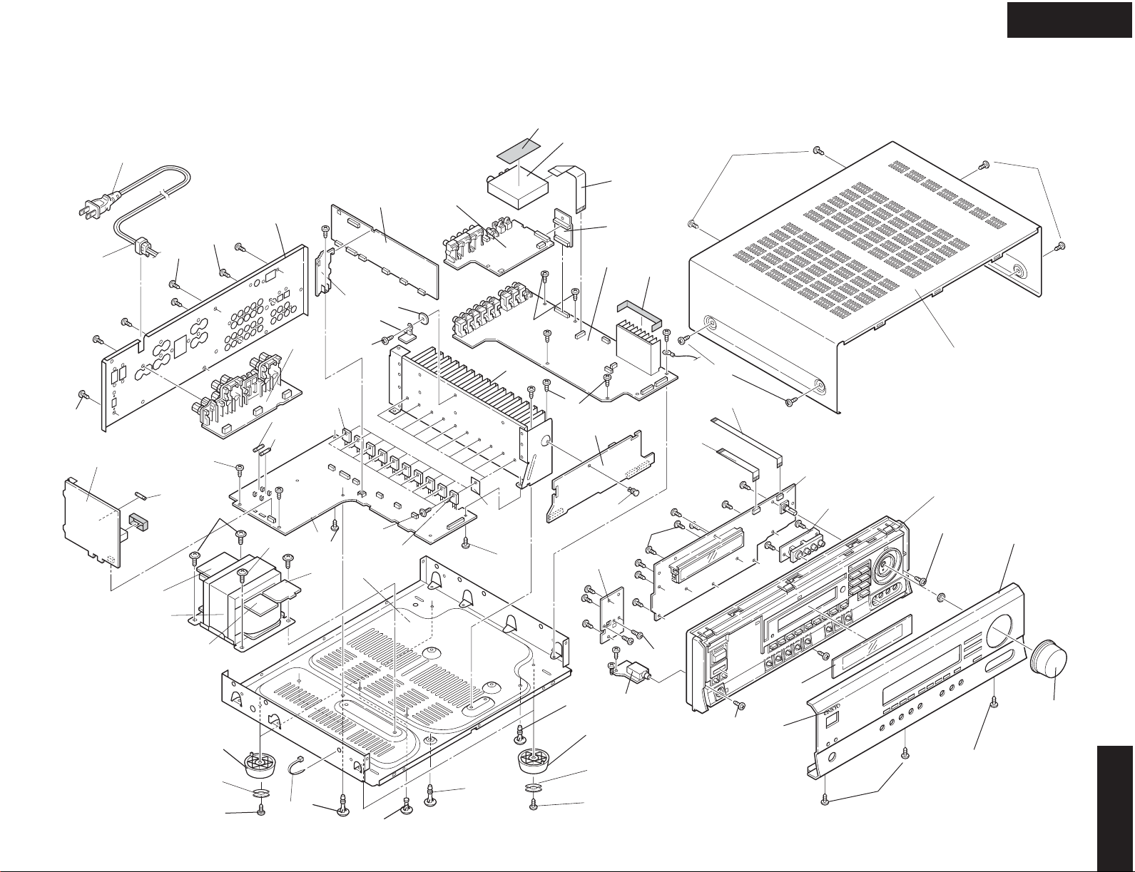
EXPLODED VIEW
P901
33
33
11
31
U12
U13
U24
HT-R500
54
U31
P101
U9
U23
2
U22
U7
U1
54
2
17
17
33
U20
U19
T901
F901
U21
2
21
22
23
12
Q6050
F6901
F6902
9
9
U17
U11
8
56
13
2
Q6064
5
7
55
2
8
2
U10
10
2
U4
3
6
U5
21
22
23
P7001
P7503
17
U3
U6
25
52
2
53
16
1
2
51
24
53
HTR-500
Page 4
HT-R500
EXPLODED VIEW
PARTS LIST
REF.NO. PART NO. DESCRIPTION
1 27111268 Fr ont br acket
2 838130088 3TTB+8B,Self-tapping scr ew
5 27100416 Chassis
6 27190503A KGLS-8RF,Holder
7827190813
27190428A
9 830440089 4TTC+8C(BC),Self- tapping screw
10 880009 NRP- 345, Plastic rivet
11 27300750 Bushing,cord
12 27160511 Heat sink
13 801433 3SM S8W. SW+14B( BC),Special screw
16 28184831 Top cover
17 838430088 3TTB+8B(BC),Self-tapping screw
21 27175319B Leg
22 28141494 Cushion
23 838130088 3TTB+8B,Self - t apping screw
24 28325641 Knob, volume
25 28191957 Clear plate
31 27122989A Rear panel
33 838430088 3TTB+8B(BC),Self-tapping screw
51 27212402 Front panel
52 28135244 Badge
5354838430088
29110083
55 223024 AC238, Isolated plate
56 260208 Wir e t ie
F6901, 252198 or 8A-UL or
F6902 252261 8A-T/UL-ST2,Fuse
F901 252198 or 8A-UL or
252261 8A-T/UL-ST2,Fuse
P101 2047151512 NCFC7-151512,Flexible flat cable
P7001 2045102012 NCFC5-102012,Flexible flat cable
P7503 2047081012 NCFC7-081012,Flexible flat cable
KGPS-10RF,Holder
KGLS-10RF,Holder
!
3TTB+8B(BC),Self-tapping screw
Tape cloth
!
!
!
!
NOTE: THE COMPONENTS IDENTIFIED BY MARK !
ARE CRITICAL FOR RISK OF FIRE AND
ELECTRIC SHOCK. REPLACE ONLY WITH
PART NUMBER SPECIFIED.
CAUTION: Replacement for transisto r of mark *, if necessary
must be made from the same beta group (h
the original type.
REF.NO. PART NO. DESCRIPTION
P901 253332HIT or AS-UC-2 or
253333VOL AS-UC-2,Power supply cord
Q6050~ 2203563, KTC5242-O,
Q6054 2202842, 2SC5242-R,
2202843, 2SC5242-O,
2203562, KTC5242-R,
2203663, MN130S-O,
2203664 or MN130S-Y or
2203666 MN130S-P,Transistor
Q6060~ 2203553, KTA1962-O,
Q6064 2202832, 2SA1962-R,
2202833, 2SA1962-O,
2203552, KTA1962-R,
2203673, MP130S-O,
2203674 or MP130S-Y or
2203676 MP130S-P,Transistor
T901 2301624 NPT-1446D,Power transformer
U1 1A928501-1F NADG-7401-1F,DSP circuit PC board ass'y
U3 1A928503-1A NADIS-7403-1A,Display circuit PC board ass'y
U4 1A928504-1A NASW-7404-1A,Standby switch PC board ass'y
U5 1A928505-1A NAETC-7405-1A,Headphone terminal PC board ass'y
U6 1A928506-1A NAETC-7406-1A,Front video PC board ass'y
U7 1A928507-1A NAETC-7407-1A,Connector PC board ass'y
U9 1A928509-2A NAAF-7409-2A, Power amplifier driver PC board ass'y
U10 1A928510-2A NAETC-7410-2A,Regulator PC board ass'y
U11 1A928511-2A NAETC-7411-2A,Secondary PC board ass'y
U12 1A928512-2A NAETC-7412-2A,Speaker terminal PC board ass'y
U13 1A928513-2A NAETC-7413-2A,PC board for holder
U17 1A928517-2A NAAF-7417-2A,Power amplifier PC board ass'y
U19 1A928519-2A NAPS-7419-2A,Terminal PC board ass'y
U20 1A928520-2A NAPS-7420-2A,Primary circuit PC board ass'y
U21 1A928521-2A NAPS-7421-2A,Terminal PC board ass'y
U22 1A928522-2A NAVD-7422-2A,Video terminal PC board ass'y
U23 1A928523-2A NAETC-7423-2A,PC board for holder
U24 1A928524-2A NAETC-7424-2A,Thermal detector circuit PC boar d ass' y
U31 240138A or ENG06501QR or
240134A TFCE1U114B,Tuner unit
!
!
*
*
*
*
*
*
*
*
*
*
*
*
*
*
!
FE) as
HT-R500
Page 5
HT-R500
+
A
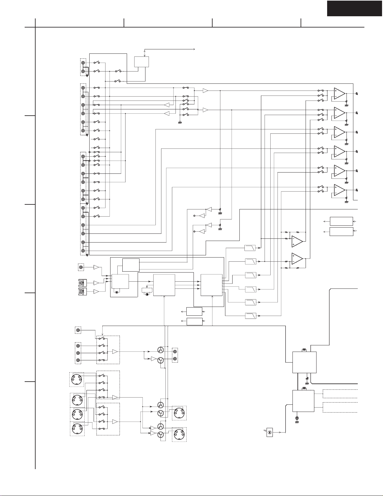
BLOCK DIAGRAM 1
80
1
2
3
4
5
VIDEO3
CD
TAPE-1 OUT
TAPE-1 IN
VIDEO-2 IN
VIDEO-1 OUT
VIDEO-1 IN
DVD
MLS/MRS
C/SW
COAXIAL
OPTICAL 1
OPTICAL 2
VIDEO3
COMPOSITE VIDEO INPUT
VIDEO2
VIDEO1
DVD
VIDEO 3
VIDEO 2
S-VIDEO INPUT
VIDEO 1
DVD
79 78
2
1
72
71
4
3
6
5
73
8
74
7
76
75
10
9
12
11
14
13
16
15
P
YC
YC
YC
YC
S
S
BD3811K1
CTLA/B
LA7956
LA7956
LA7956
77
AK4586
2CH A/D
DIR
AK4586
12.288MHZ
6dB
6dB
6dB
(1/2)
96/24
FM/AM
TUNER
PACK
OSC
12.288MHZ
BCD
To/From Main Microrocessor
INPUT GAIN
0/6dB
INPUT GAIN
INPUT GAIN
INPUT GAIN
INPUT GAIN
INPUT GAIN
+7V
BD3811
-7V
BD3811
KEY
FL DISPLAY
0/6dB
0/6dB
0/6dB
0/6dB
0/6dB
69
66
43
40
30
33
-
CS493293
(MJJ ONLY)
CS493264
RST.CS.INTREQ
0dB
RN1441
0dB
0dB
1
1
17
DSP
/CL/DA/SCDO
VMUT1
VMUT2
COMPOSITE VIDEO OUT
MONITOR OUT
VIDEO 1
YC
YC
1
1
1
18
-1
NC
1
20
-1
NC
19
AK4586
96/24
6CH D/A
AK4586
+2.5V
+5V
DSP
+3.3V
+5V
MEMORY
S-VIDEO OUTPUT
MONITOR OUT
VIDEO 1
-6DB
INPUT ATT
RST.CS/CL/DA
/CDTO/INT1.2.
SW
SL
SR
50KLPF
L
50KLPF
R
50KLPF
50KLPF
50KLPF
C
50KLPF
2321262528
REMOTE
SENSOR
27
9.97K
10K
10K
9.97K
OPAMP
10K
10.5dB
10K
O
P
A
M
P
12.5MHZ
MAIN
MICRO
PROCESSOR
UPD784225
AGC
SUBMICRO
PROCESSOR
UPD780232
GC-8BT
STANDBY
24
5MHZ
22
BACK UP
Page 6

HT-R500
Y
A
BLOCK DIAGRAM 2
1
T GAIN
0/6dB
AIN
AIN
0/6dB
GAIN
2
AIN
GAIN
0/6dB
0/6dB
0/6dB
0/6dB
MASTER
VOLUME
0,,-103dB
68
69
65
66
42
43
39
40
31
30
34
33
OPAMP
OPAMP
OPAMP
OPAMP
OPAMP
OPAMP
OUTPUT GAIN
0-18dB
OUTPUT GAIN
0-18dB
OUTPUT GAIN
0-18dB
OUTPUT GAIN
0-18dB
OUTPUT GAIN
OUTPUT GAIN
0-18dB
0-18dB
36
BASS/TREBLE
BASS/TREBLE
Q305
OPAMP
15dB
BASSBOOST
38
37
35
BCD
Power Amplifier
2.2K
55
47/16
2.2K
57
47/16
2.2K
47/16
2.2K
47/16
2.2K
47/16
47/16
270
R388
100
R385
100
C352
104Z
SWPO
P351
+27dB
+27dB
+27dB
+27dB
+27dB
HEADPHONE
L
R
C
SL
SR
SPBL
SPBR
7V
D3811
-7V
D3811
+12V
-12V
AMUT
Q306
OR KRA102S
3
VOLTAGE &
CURRENT
SENSOR
VOLTAGE
SENSOR
SELMUT
SELDA
SELCL
SEC1H
SEC1H
CONTROL
+5.6V
4
STANDBY
-27V
-VP
+12V
VIDEO
+12V
AF/TU
-12V
AF
+5V
DSP/TU
ISPLAY
SEC1H RELAY
+B1
RELAY
+B2
FLAC
FL TUBE
FLAC
+B1H
+B1L
VOLH
SEC1
SEC2
SEC3
T902
PROTE
CTION
PRO
PRI
T901
FUSE
SPHP
SPF
HPMUT
SPB
SPCS
HPDET
POWER
POWER
RELAY
AC OUTLET
AC IN
5
RI
INTERFACE
RI
Page 7

HT-R500
A
SCHEMATIC DIAGRAM 1
Display section
NADIS-7403
1
F2F2NPNPP35
P34
P33
P32
P31
P30
5556575859
2
R7582
*
100K X 13
Q7504
D7502
UDZ5.1B
R7505
220K
RN2403
*KRA103S
D7503
1SS352
R7532
10K
R7504
47K
R7506
R7507 4.7K
P29
SYSOUT
4.7K
P28
P27
C7507
104Z
BCD
Q7501 HNA-16MM39T
P26
P25
P24
P23
P22
P21
P20
P19
P18
P17
P16
P15
P14
P13
P12
P11
P10P9P8P7P6P5P4P3P2P116G
R7581
100K X 14
*
41
42
43
P46/FIP3840
P47/FIP3939
P50/FIP4038
P51/FIP4137
P52/FIP4236
P53/FIP4335
P54/FIP4434
P55/FIP4533
P56/FIP4632
P57/FIP4731
P60/FIP4830
P61/FIP4929
P62/FIP5028
P63/FIP5127
P64/FIP5226
VDD025
AVDD24
22:ANI0
VSS023
21:ANI1
22
21
ANI220
ANI319
4.7K
4.7K
R7509
R7508
P42/FIP34 44
41:P45/FIP37
42:P44/FIP36
AVSS18
P02/TI17
1K
R7510
R75111KR7512
P37/FIP31 47
P40/FIP32 46
P41/FIP33 45
43:P43/FIP35
P01/INTP116
P20/SCK314
POO/INTP015
10K
10K
10K
R7513
R7514
P34/FIP28 50
P35/FIP29 49
P36/FIP30 48
Q7502
UPD70232GC
-30-8BT
P21/SO313
P2212
P2311
10K
10K
R7515
R7516
P31/FIP25 53
P32/FIP26 52
P33/FIP27 51
P24/BUSY10
P25SO19
P26/SI18
P27/SCK17 P30/FIP24 54
FIP22 56
FIP23 55
61:FIP19
RESET
IC5
6
FIP20 58
FIP21 57
X13
X2
4
VDD2 59
VLOAD 60
FIP18 62
FIP17 63
FIP16 64
FIP15 65
FIP14 66
FIP13 67
FIP12 68
FIP11 69
FIP10 70
FIP9 71
FIP8 72
FIP7 73
FIP6 74
FIP5 75
FIP4 76
FIP3 77
FIP2 78
FIP1 79
FIP0
VDD11
VSS12
X7501
CST5.00MGW
15G
14G
13G
12G
11G
10G9G8G7G6G5G4G3G2G1GNPNPF1
101112131415161718192021222324252627282930313233343536373839404142434445464748495051525354
61
80
F1
123456789
104Z
104Z
C7502
C7501
33/50
C7503
C7504
R7580 10K X 15
*
R7501 220
473Z
C7505
473Z
220
R7502
D7501 UDZ8.2B
C7506
104Z
R7614
820
C7514 100/6.3
C7516
C7515
S7614
STANDBY
R7613
560
NASW-7404
104Z
104Z
102J
C7517
JL7501B
102J
102J
102J
C7508
VIDEO3
TUNING<
PRESET>
2.7K
R7521
C7510
C7509
220
R7531
D7505
STANDBY
Q7506
RN1402
*KRC102S
S7625
S7635
S7645
2.7K
R7522
10K
R7527
102J
2.7K
C7511
R7523
10K
R7526
U3
VIDEO2
MEMORY
PRESET<
K2
2.7K
R7520
K0
K1
SYSIN
JL7501A
GND
KEY0
R7626
2.2K R7621 330R7625 1.2K R7624 820 R7623 560 R7622 470
S7626
S7627
FM MODE
S7637
S7636
TUNING<
R7646 2.2K
AUDIO
S7646
S7647
ADJUST
K3
S7624
S7634
S7644
STBYLED
VIDEO1
TAPE
DSP
101J
R7524 1K
SBMRST
SEL
C7522
104Z
C7513
C7523 102J
100K
K3
K0K1K2
INPUT
S7611
DIGITAL
S7621
DISPLAY
330R7632 470R7633 560R7634 820R7635 1.2KR7636 2.2K
SP
S7631
ADJUST
SYSIN
HPDET
SBMDI
SBMDO
S7641
DIRECT
SBMLDY
SBMCLK
SBMRST
L7505
-VP
220K
NCH1477
P7502A
R7519
P7503A
D7507
1SS352
L7504
+5.6S
C7521
220/6.3
220K
NCH1477
HPR
HPE
TO NAETC-7410 <SCH-6>TO NADG-7401 <SCH.2-2>
TO NAETC-7405 <SCH.3>
JL7502A
FAC2
FAC1
HPL
GND
GND
100K
R7518
IRF
1K
1K
560
560
VAJ
VBJ
R7517
R7530
R7529
R7528
SBMDI
SBMDO
SBMLDY
SBMCLK
R7612
470 R7611 330
S7612
S7613
DIMMER
SW MODE
DVD
S7622
TUNER
SURROUND
S7632
S7642
AUDIO
R7631
CD
R7641 330R7645 1.2K R7644 820 R7643 560 R7642 470
STEREO
S7623
S7633
S7643
3
U7501
SPS4441E1
S7501
S7616
S7615
SP B
SP A
4
R7615
1.2K
U4
5
Page 8

5
5
7
8
1
1
C361
4
4
4
4
C
HT-R500
A
SCHEMATIC DIAGRAM 2-1
R300
CDR
330
104Z
C308
101J101J
C301 C300C321 C320 C319 C318 C317 C316 C315 C314 C313
330
CDL
R301
R302
TOR -12VAF
330
C302
101J
101J
C303
330
TOL
R303
R304
TIR
330
101J
101J
330
TIL
R305
R306
V3IR
330
101J 101J
C307 C306 C305 C304
330
V3IL
R307
R310
V2IR
330
101J
101J
C311 C310
330
V2IL
R311
R312
V1OR
330
101J
C312
101J
330
V1OL
R313
R314
V1IR
330
101J
101J
330
V1IL
R315
R316
DVDR
330
101J
101J
330
DVDL
R317
R318
330
330
101J 101J
R319
R320
MSW
330
101J
101J
330
MC
R321
CD
1
TAPE-1 OUT
TAPE-1 IN
P301
C322
P302
P304
P305
104Z
C323
103Z
C325
104Z
C326
104Z
TUNER
VIDEO-2 IN
2
VIDEO-1 OUT
VIDEO-1 IN
DVD
MLS/MRS
C/SW
3
BCD
DSP section
P261A
TO NAETC-7406
<SCH.3>
TUL
TUR
C329
C330
10/16
10/16
TOR
TOL
V1OL
V1OR
V4R
V4L
TUL
TUR
77
78
79
80
CDR
CDL
TIR
TIL
V3IR
V3IL
V2IR
V2IL
V1IR
V1IL
DVDR
DVDL
MRS +7V
MLS
MSW -7V
MC
ADCL SELMUT
ADCR SELDA
DAC_R
DMIXR
DAC_L
DMIXL
1
2
3
4
5
6
7
8
9
10
11
12
13
14
15
16
17
18
19
20
21
22
23
24
7
10K
C327
330J
330J
C328
10K
1
47k
47k
47k
47k
47k
47k
47k
47k
47k
47k
47k
47k
47k
47k
47k
47k
47k
47k
47k
47k
47k
47k
47k
DAC_RS
DAC_LS
8
Q302
R361
NJM4565M
OR MPC4570
R362
Q302
4
NJM4565M
OR MPC4570G2
47k
47k
47k
47k
272625
DAC_SW
5
6
2
3
28
DAC_C
R347
R348
47k
297032
10/16
C334
10K
10K
30
31
DAC_L
10/16
C333
7273747576
33
71
Q301
BD3811K1
34
35
OUT_C
69
363738
OUT_LS
OUT_SW
68
OUT_RS
67
66
65
C335
64
C336
63
C337
62
61
C339
60
59
C340
58
563J
57
56
55
54
C345
C347
53
100/16
104Z
52
BAAS BOOST BASS TREBLE
VCC
51
50
VEE
C346
104Z
49
MUT
48
CL
SELCK
47
DA
46
45
44
43
42
41
40
39
C332
10/16
OUT_SW
OUT_C
DAC_SW
DAC_SW
2.7K
R386
R360
270
332J
R363
C338
R364
OUT_L
OUT_R
100/16
R359
R387
104J
10K
C348
10/16
332J
104J
10K
563J
C331
270
2.7K
+7V
-7V
C359
10/16
Q322 79L07
C362
10/16
O
O
78L07
Q321
10/16
G
G
C349
I
I
C367
1K
R367
C366
104Z
104Z
2.2K
R369
R370
47K
C350
221J
R368
+12VAF
NJM4565M
OR MPC4570G2
2
3
22K
6
5
C6404
10/16
C6406
10/16
C6410
10/16
C6412
10/16
330J
C351
R383 10K
Q305
8
Q305
4
-12VAF
+12VAF
+12VVD
+5VDSP
R6402
Q6402
10
O
I
G
Q6403
O
G
Q6405
O
G
Q6406
O
G
OUT_R
OUT_RS
OUT_LS
OUT_C
NJM4565M
OR
MPC4570
C6403
223Z
I
C6405
223Z
I
C6409
223Z
I
C6411
223Z
OUT_L
R6403
33
R6410
C353
47/16
47/16
47/16
1/2W
1/2W
R6407
R6408
2.2
C354
C358
1/2W
1W
3.3
8.2
1/2W
R330
470
R331
470
R373
470
470
R374
R375
470
270
R376
R384
220K
78M12
79M12
78M12
78M05
7
1
Q307 RN1441
Q308
Q312
100
RN1441
R388
474K
RN1441
RN1441
C360
+22V
C9512
223Z
GND
-22V
GND
RN2402
-VP
2SA101
KTA12
R9509
100K
D9508
UDZ2
C640
104J
P6403
22K
R377
22K
R378
22K
R379
22K
R380
22K
R381
22K
Q313
R382
RN1441
224K
Q306
OR KRA102S
Q9
C365
+7V
C801
47/16
R804
R803
L805
C803
CDA
R806
R805
C802
150J
150J
1
GND4
R739 1M
X701 CSTCV12.2MTJ0C4
SRDA
LRDA
SDTO
BCK
LRCK
MCK2
BK1608LM182
C817
R821
470
150J
+5VDSP
NADG-7401
152J
4
5
DAC_C
DAC_SW
DAC_LS
DAC_RS
DAC_L
DAC_R
-7V
+7V
10/16
47/16
10/16
10/16
10/16
GND
10/16
C854
C855
C856
C857
C858
C859
7
NJM4565M
NJM4565M
1
7
NJM4565M
NJM4565M
1
7
NJM4565M
NJM4565M
1
Q802
Q802
153J
Q803
Q803
152J
152J
Q804
Q804
152J
C848
4
5
6
2
3
8
C849
C850152J
4
5
6
2
3
8
C851
C852
4
5
6
2
3
8
C853
2.2K
R849
2.2K
R850
2.2K
R851
2.2K
R852
2.2K
R853
2.2K
R848
C840
C841
C842
C843
C844
C845
C832
R840
2.2K
10/16
821J
R832
100K
R833
100K
822J
C833
R841
2.2K
10/16
C834
R842
2.2K
10/16
821J
R834
100K
R835
100K
821J
C835
R843
2.2K
10/16
C836
R844
2.2K
10/16
821J
R836
100K
R837
100K
821J
C837
R845
2.2K
10/16
ADCL
ADCR
47/6.3
C364
104Z
C808
104Z
C809
47/6.3
C363
C807
10/16
104Z
D801
D802
C816
C806
220/6.3
VREFH
AVDD
23
24
VCOM
25
DFZ1
26
LOUT3
27
ROUT3
28
LOUT2
29
ROUT2
30
LOUT1
31
ROUT1
32
LIN
33
RIN
PVDD
3435363738394041424344
C810
47/16
C811
104Z
R815
P802
AVSS
R
C800
220
R814
18K
DFZ2
PVSS
DIRCS
330J
R816
220
R813
CSN
RX4
C812
330
DSPDO
DSPSCK
220
R812
CCLK
Q801
SLAVE
330J
R817
RX3
CDTI
AK4586
RX3
CDTO/SCDO[L]
INT1[L]
INT0[L]
220
R8101KR811
R809 1K
CDTO
INT1
INT0
I2C
RX2
TST
C814
C813
330J
330
330
R818
RX2
+5VDSP
GND
47
R808
R819
RX1
330J
SDTI3
RX1
47
R807
1213141516171819202122
SDTI1
SDTO
BICK
LRCK
MCKO
TVDD
DVSS
DVDD
PDN
DIRPD
330 R820 10K
TX
+3.3V
GND
022M
L804
SDTI2
11
47
10
47
9
47
8
47
7
6
TX
R801
47
5
C805104Z
4
C804
104Z
3
2
XTI
1
XTO
L803
022M
022M
L801
022M
L802
C815
102K
104Z
C715
VCC
Q707
TC7WU04FU
8
72
63
5
NCH-147
L704
L706
022M
BK1608LM1
L705
BK1608LM1
103K
LRCK
DSPMCK
DSPRST1[L]
+2.5V
1
1
1
1
U1
Page 9
HT-R500
A
BCD
SCHEMATIC DIAGRAM 2-2
DSP section
TO NADIS-7403
P801Q9501
C106
101J
KRC104S
Q7007
KRC104S
RN1404
1K
470
220
R7034
R7032
R7134
C7008
104Z
X7001
CSTCV12.5MXJ
MPC2925T
Q7004
C7011
47/16
Q7005
MPC2933T
O
C7012
47/16
TX
RN1404
220
R7031
Q7008
G
G
C729
RX1
+5VDSP
Q7006
VMUT1
VMUT2
220
220
R7029
R7030
MPD784225
R7071
4.7K
IO
I
C7014
104Z
<SCH.1>
RX2
GND
CTLB
CTLA
220
220
R7028
R7027
104Z
C7013
NCH-1479
104Z
C7015
C721
104Z
RX3
POWER
220
R7026
C7009
104Z
L7002
VMUT1
SPF
220
R7025
R7076
1K
RDSDATA
470M
47/16
VMUT2
SPCS
220
R7024
1K
RDSSIG
GND
CTLB
CTLA
GND
RI
SPB
SEC1H
220
220
2.2K
R7023
R7022
R7021
21222324252627282930313233343536373839
R7120
R7020
20
R7019
19
R7018
18
R7017
17
R7016
16
R7015
15
14
13
R7012
12
R7011
11
10
9
8
C7003
7
6
5
4
R7003
3
R7002
2
R7001
1
80
1K
R70781KR7077
R7080
1K
1K
R7179
R7180
1K
NADG-7401
R187
1K
47K
C730
+12VVD
220
220
82
82
82
82
220
1K
104Z
10K
2.2K
2.2K
R186
47K
R185
47K
104Z
R7000
VOLH
C7001
HPIN
100
RI
HPIN
MCRDY
P7502B
TO RS232C
P7701
MCSDA
MCMDA
MCCLK
MCRST
HPMUT
MCRDY
MPURST
MCMDA
MCSDA
-VP
FVCC
MCCLK
GND
D7702
IC
TO SUB MPU
P412B
UDZ6.2B
FLASH
HPMUT
MCCLK
MCMDA
MCSDA
MCRDY
232TXD
232RXD
PROTECT
D7001
104F
C7002
100/6.3
220K
L7001
NCH-1477
U1
104Z
C722
C731
100/6.3
D9502-9505:
-VP
2SA1015-GR
R9506
KTA1266-GR
C9512
223Z
(/2W
1
GND
R9509
C9511
2V
100K
223Z
D9508
-22V SPB
UDZ27D
GND
C6401
104J
P6403
1
22K
R377
22K
R378
1
2
1
Q313
RN1441
OR KRA102S
R379
R380
R381
R382
Q306
22K
22K
22K
22K
224K
C365
AMUT
C361
222J
R385
100
3
NCH-1471
L704
L706
022M
BK1608LM182
L705
BK1608LM182
2MTJ0C4
4
DSPMCK
C708
33K
103K
LRCK
C709105K
R719330
R72047
DSPMCK
R721
4.7K
105K
C710
471J
C711
104Z
C712
R722
1K
4.7K
R723
R724
4.7K
DSPRST1[L]
R725
47
C713
101J
C716
100/6.3
L701
+2.5V
NCH-1471
022M
5
RL1N4003
1SR154-400
22
R9508
15K
220/63
RSPO
LSPO
C9510
C9508
4700/16
LPO
GND
RPO
GND
CPO
SWPO
R718
C9507
D9507
220/35
R9507
15K
D9506
1SR154-400
P406
104Z
C352
GND
NCH1471
L702
022M
D9505
C9505
2200/35
C9506
470/35
D9504
D9509
D9510
D9511
D9512
P306
P351
C717
104Z
+3.3V
BCK
BCK
LRCK
SDTO
R715
R716
R717
330
330
330
LRCKN126LRCLK42
CMPREQ/LRCLKN229 DATA017
CLKIN30
CMPCLK/SCLKN228
CLKSEL31
FILT232
FILT133
CMPDAT/RCV958/SDATAN2 27
VDDA34
VSSA35
RESET36
DD37
AUDATA239
AUDATA041
AUDATA140
47
LRDA
R714
330
VSS324
MCLK44
SCLK43 SCLKN1/STCCLK2 25
R729
47
MCK2
D9503
D9502
C9503
104J
SDTO
C707
R71347
104Z
VDD323
SDTAN122
Q701
CS493264-CL
VSS12
VDD11
C714
R73047R72847R72747R726
104Z
C9502
104J
C9501
104J
GND10
Q7002 TC74VHC541FT
Y8
11
R7067
220
DSPCS1[L]
INTREQ1
DSPCS1[L]
CDTO/SCDO[L]
R707
R706
R708
220
220
220
EXTMEM
R71247
10K
10K
20CS18
21
EXTMEM
DATA116
SCDIO/SCDOUT19
ABOOT/_INTREQ
DATA215
DATA314
VSS213
VDD212
DATA411
DATA510
DATA6 9
DATA7 8DC38
A0/SCCLK 7
RD/R/_W
A1/SCDIN6
XMT9583
WR/DA4
5
R701
R702
47
330
R703
4.7K
A5 6
A6 7
A7 8
A8 9
Y415
Y514
Y613
Y712
R7072
R7070
R7069
R7068
220
220
220
220
A161[L]
A171[L]
A151[L]
FMEM/SRAM1[L]
R709
R710
R71110K
C703
10K
101J
C701
C702
101J
A3 4
A4 5
Y217
Y316
R7075
R7074
R7073
220
220
220
DSPCL[3.3V]
C706
100/6.3
R704
R705
DSPCL[3.3V]
A1 2
A2 3
Y118
G2
19
DSPRST1[L]
470M
L703
NCH-1479
104Z
330
P101
TO TUNER PACK
SD
TUR
GND
TUL
DET
TMUT
STEREO
22K
22K
R102
R103
SELMUT
AMUT
SELCK MCRST
SELDA
SNONE
SWNONE
CNONE
DIRCS
DSPCS
ROM/RAM
A151
A161
A171
DSPSCK
DSPDO
DSPRST
CDTO/SCDO
INT1
INT0
DIRPD
Q7001
C7005
100/6.3
D7002
1
G1
C7010104Z
VCC20
DSPDA[3.3V]
10K
220
220
1K
1K
1K
220
220
1K
1K
1K
1K
220
220
220
1K
1K
1K
220
KRC104S
RN1404
1/50
C7004
D7004
1SS352
TC74HCT7007
Q7003
9
220
R7081
CDTO/SCDO
CDTO/SCDO[L]
104Z
C720
+12VAF
FMSIG
+5VDSP
PLLCL
PLLDA
PLLSTB
GND
C101
3.3/50
R7041
R7042
R7043
R7044
R7045
R7046
R7047
R7048
R7049
R7050
R7051
R7052
R7053
R7054
R7055
R7056
R7057
R7058
R7059
R7060
R7083
101112
220
INT1
INT1[L]
C7006
104Z
47K
220
R7082
INT0
47K
R7033
13
220
INT0[L]
100K
101J
R104
C103
C104
3.3/50
22K
22K
R7138
R7839
TMUT
SD
PLLCL
PLLDA
PLLSTB
STEREO
220
220
220
220
2.2K
2.2K
R7035
R7037
R7038
R7039
R7040
R7036
40
41
42
43
44
45
46
47
48
49
50
51
52
53
54
55
56
57
58
59
60
61626364656667686970717273747576777879
104Z
R7062
R7066
R70651KR70641KR7063
C7007
220R7084
12345678
14
POFF
R7085
D7003
220K
1K
1K
RDSSCK
INTREQ1
+2.5V +5VDSP
+3.3V
SEC3-1
SEC3-2
5.6S
SEC1-2
SEC1-1
+13V
+22V
GND
TO NAETC-7410
<SCH.6>
POWER
SPF
SPCS
P411B
SEC1H
VOLH
PROTECT
GND
TO NAETC-7410
P410B
TO NAETC-7410
DSPDA[3.3V]
Page 10

HT-R500
A
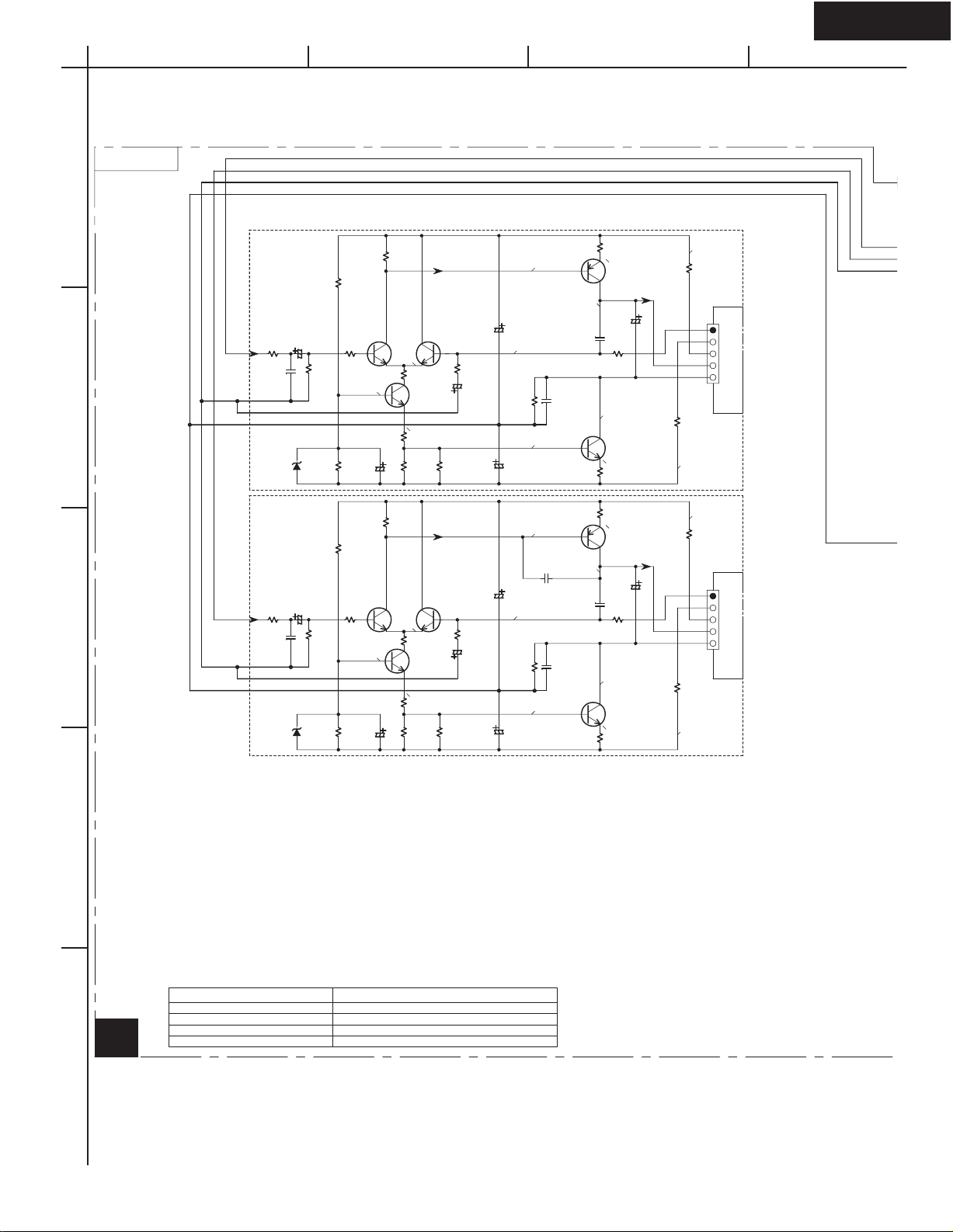
SCHEMATIC DIAGRAM 3
NCETC-7407 NAVD-7422
U7
P206A
+12V
GND
1
<SCH-2-2>
NADG-7401
2
<SCH-3>
NAETC-7406
P253A
P206B
3
4
P801B
V4
V4Y
V4C
+12V
GND
A
B
VMUT2
VMUT1
RI
OPT2
DGND
OPT1
+5V
COAX
OPTOUT
VMUT2
VMUT1
OPT2
DGND
OPT1
OPTOUT
+5V
COAX
A
B
RI
C217
C218
C219
2.2/50
2.2/50
223Z
VIN4
VIN3
VCC
LA7956
VIN2
GND
VIN1
Q203
VIDEO OUT
VIN4
VIN3
VCC
LA7956
VIN2
GND
VIN1
Q212
VIDEO OUT
VIN4
VIN3
VCC
LA7956
VIN2
GND
VIN1
Q213
VIDEO OUT
BCD
Video section
U22
C227 223Z
C201
Q202
C206
C207
C208
C209
C214
223Z
C215
100/16
C203
100/16
RN1241
R224
2.2/50
C210
223Z
C211
100/16
2.2/50
R227
14
13
12
11
10
9
R207
R208
R209
R223
100K
100K
223Z
223Z
2.2/50
C212
680K
680K
680K
100/16
R225
R226
680K
680K
R221
R222 75
C283
223Z
R284 10K
2.2/50
R205
C202
2.2/50
C204
2.2/50
C205
75
680K
R212
R219
R220 75
75
R214
223Z
75
100K
R218
C284 080D
75
C220
223Z
75
75
R216
C216
223Z
R206
75R217 100K
R211
75
R213
R203
75
R204
R215 75
C281
223Z
R281 75
75
R201
75
R202
75
100K
YC
YC
YC
L283
022M
101J
C282
C287
C288
9
8
7
6
5
4
3
B
2
A
1
R229
9
8
7
6
5
4
B
3
A
2
1
9
8
7
6
5
4
3
B
2
A
1
680K
C221
47/16
C222
223Z
C223
47/16
C224
223Z
C225
47/16
C226
223Z
L282
L281
NCH-1452
NCH-1452
R230
680K
220K
220K
C286
R210
223Z
220
Q204
2SA933-S
*KTA1267-GR
DTA114ES
*KRA102M
DTA114ES
*KRA102M
Q209
2SA933-S
*KTA1267-GR
Q205
Q206
C285
R228
Q211
47/6.3
Q201
RN1241
220
Q210
RN1241
RN1241
1
2
3
4
5
6
7 8
Q207
Q208
RN1241
RN1241
C213
Q281
74HCU04
CY
CY
223Z
47/6.3
P201
OUT
VIDEO-1
IN
P202
DVD IN
MONITOR
OUT
P203
VIDEO-2
P201
OUT
VIDEO-1
IN
P202
DVD IN
P203
MONITOR
U281
U282
INVIDEO-2
IN
P281
P7501
HPDET
GND
<SCH-1>
NADIS-7403
5
HPL
HPE
HPR
JL7502B
E7501
C7518
102J
C7519
102J
C7520
102J
U5
HEADPHONE
NAETC-7405
NAETC-7406
YC
R253
<SCH-3>
NAVD-7422
75
P253B P261B
VIDEO3 IN
SRLV
P251
U6
R252 75R251 75
C253
104Z
P254
C263
104Z
330
C261C262
R261
101J
101J
<SCH-2.1>
NADG-7401
330
R262
R282
470
P282
Page 11
HT-R500
E
A
SCHEMATIC DIAGRAM 4-1
NAAF-7409
1
SL
C5013
R5003
100/16
1K
D5003
SR
1K
D5004
C5014
100/16
R5013
56K
R5103
100K
R5014
56K
R5104
100K
C5003
101K
2
MTZJ5.6B
R5004
3
C5004
101K
MTZJ5.6B
BCD
Power amplifier section 1
R5113
1K
R5093
100K
Q5013Q5003
C5103
10/100
R5063
1.2K
R5114
R5064
1.2K
1K
-0.9V
R5053
4.7K
Q5053
-59.1V
R5073
560
-0.9V
R5054
4.7K
Q5054
-59.1V
R5074
560
R5043
2.2K
C5043
220/16
R5133
R5083
3.3K
Q5014Q5004
C5104
10/100
R5044
2.2K
C5044
220/16
R5134
R5084
3.3K
R5023
330
-44.3V
C5023
10/50
R5094
100K
R5024
330
C5024
10/50
-57.4V
62.1V 62.7V
C5083
0V
18K
C5093
101J
-62.1V
C5113
10/100
0V
18K
C5114
10/100
62.1V
C5074
-62.1V
R5173
120(1/4W)
C5084
C5094
101J
R5174
120(1/4W)
1.1V
040D
1.1V
040D
R5163
120(1/4W)
Q5033
C5053
47/50
R5033
56K
-1V
Q5043
-62.7V
R5164
120(1/4W)
62.7V
Q5034
C5054
47/50
R5034
56K
-1V
Q5044
-62.7V
R5183
10
(1/4W)
R5184
10
(1/4W)
63V
NF
-B1
+B1
B+
B-
R5193
10
(1/4W)
-63V
63V
NF
-B1
+B1
B+
B-
R5194
10
(1/4W)
-63V
P6003A
TO NAAF-7417
P6004A
TO NAAF-7417
P406A
(SCH.5-1)
(SCH.5-1)
4
SEMICONDUCTORS
U9
NO.
Q5000-04,5010-14 KTC3200-BL OR 2SC1775A-E,F OR 2SC1845-E
Q5030-34 KTA1024-Y,O OR 2SA949-Y,O
Q5040-44 KTC3206-Y,O OR 2SC2229-Y,O
Q5050-54 KTC3200-BL,GR OR 2SC1775A-E,F OR 2SC1845-E,F
5
Page 12
HT-R500
A
SCHEMATIC DIAGRAM 4-2
Power amplifier section 2
TO NADG-7401
1
406A P306A
EEC
2
3
(SCH.2-2)
ESLESRERE
E
E
E
E
E
E
(SCH.5-2)
E
TO NAAF-7417
E
E
P6011A
L
L
R5000
1K
C5000
101K
D5000
MTZJ5.6B
R
R5001
1K
C5001
101K
D5001
MTZJ5.6B
C5010
100/16
C5011
100/16
BCD
NAAF-7409
R5010
56K
R5100
100K
R5011
56K
R5101
100K
R5090
100K
R5020
330
C5020
10/50
R5091
1
0
0K
R5021
330
-57.4V
C5021
10/50
0V
-57.4V
R5110
R5060
1.2K
R5111
R5061
1.2K
1K
1K
-0.9V
R5050
4.7K
Q5050
-59.1V
R5070
560
-0.9V
R5051
4.7K
Q5051
-59.1V
R5071
560
R5160
120(1/4W)
1.1V
C5080
040D
R5170
1.1V
C5081
040D
R5171
62.7V
Q5030
C5050
47/50
R5030
56K
-1V
Q5040
-62.7V
R5161
120(1/4W)
62.7V
Q5031
C5051
47/50
R5031
56K
-1V
Q5041
-62.7V
62.1V
Q5010Q5000
C5100
10/100
R5040
2.2K
C5040
220/16
R5080
3.3K
Q5011Q5001
C5101
10/100
R5041
2.2K
C5041
220/16
R5081
3.3K
0V
R5130
18K
C5110
10/100
0V
R5131
18K
C5111
10/100
-62.1V
62.1V
-62.1V
C5090
101J
120(1/4W)
C5091
101J
120(1/4W)
R5180
10
(1/4W)
R5181
10
(1/4W)
63V
NF
-B1
+B1
B+
B-
R5190
10
(1/4W)
-63V
63V
NF
-B1
+B1
B+
B-
R5191
10
(1/4W)
-63V
P6000A
(SCH.5-2)
TO NAAF-7417
P6001A
(SCH.5-2)
TO NAAF-7417
C
R5112
1K
R5092
100K
4
C5012
R5002
100/16
1K
R5012
R5022
56K
R5102
100K
330
-57.4V
C5022
10/50
R5062
C5002
101K
D5002
MTZJ5.6B
1.2K
-0.9V
R5052
4.7K
Q5052
-59.1V
R5072
560
Q5012Q5002
C5102
10/100
R5042
2.2K
C5042
220/16
R5082
3.3K
62.1V 62.7V
0V
R5132
18K
C5092
101J
-62.1V
C5112
10/100
120(1/4W)
1.1V
C5082
040D
R5172
R5162
(1/4W)
120
Q5032
C5052
47/50
R5032
56K
-1V
Q5042
-62.7V
R5182
10
(1/4W)
NF
-B1
+B1
R5192
10
(1/4W)
-63V
63V
P6002A
B+
B-
(SCH.5-2)
TO NAAF-7417
U9
5
SEMICONDUCTORS
NO.
Q5000-04,5010-14 KTC3200-BL OR 2SC1775A-E,F OR 2SC1845-E
Q5030-34 KTA1024-Y,O OR 2SA949-Y,O
Q5040-44 KTC3206-Y,O OR 2SC2229-Y,O
Q5050-54 KTC3200-BL,GR OR 2SC1775A-E,F OR 2SC1845-E,F
Page 13

HT-R500
TO NAAF 7409 TO NAAF 7409 TO NAAF 7409
A
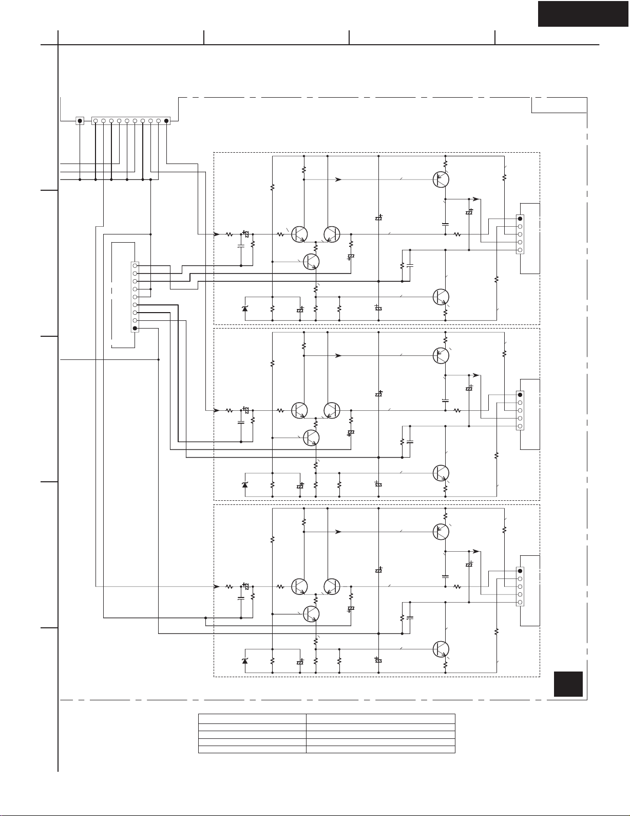
SCHEMATIC DIAGRAM 5-1
NAAF-7417
SL
R6033
1
(SCH.4-1)
TO NAAF-7409
SR
2
(SCH.4-1)
TO NAAF-7409
120
R6003
5.6K
P6003
R6013
3.9K
NF
-B1 E
+B1
B+ E
B- E
R6043
1K
R6053
3.9K
R6034
120
R6004
5.6K
P6004
R6014
3.9K
NF
-B1
+B1
B+
B-
R6044
1K
R6054
3.9K
[1V]
[0.2V]
R6023
[-0.3V]
[1V]
[0.2V]
R6024
[-0.3V]
[1.1V]
Q6013
[-0.3V]
[-63.1V]
[1.1V]
Q6014
[-0.3V]
[-63.1V]
Q6023
[-1V]
Q6043
Q6024
[-1V]
Q6044
[0.5V]
R6073
110
(1/4W)
[0.5V]
R6074
110
(1/4W)
Q6033
C6043
47/50
[-0.5V]
Q6034
C6044
47/50
[-0.5V]
BCD
Power amplifier section 3
[63.1V]
Q6053
[0V]
R6103
0.22
X2(2W)
R6153
[0V]
Q6063
R6173
47K
D6003
[63.1V]
Q6054
[0V]
R6104
0.22
X2(2W)
[0V]
Q6064
R6174
47K
D6004
R6143
22K
4.7K
R6144
22K
R6154
4.7K
R6163
33K
Q6073
C6053
R6183
47K
R6164
33K
Q6074
C6054
R6184
47K
R6133
C6033
R6134
C6034
(1/4W)
P6083
ID+
ID-
R6093
(1/4W)
(1/4W)
P6084
ID+
ID-
R6094
(1/4W)
R6083
2.2
2.2
[-0.5V]
8.2 (1W)
R6084
2.2
2.2
[-0.5V]
8.2 (1W)
[0.5V]
C6233
473J
R6233
[0.5V]
C6234
473J
R6234
C6512
R6512
(1/2W)
C6522
R6522
(1/2W)
R6513
(1/2W)
C6513C6523
R6523
(1/2W)
U17
E
E
E
E
E
E
P6011
(SCH.4-2)
TO NAAF-7409
3
4
5
TO NAPS-7420
SEMICONDUCTORS
NO.
Q6010-6014 2SC1740S-R,S
Q6020-6024 2SC1740S-R,S
Q6030-6034 KTD2061-Y OR 2SC5171
Q6040-6044 KTB1369-Y OR 2SA1930
Q6050-6054 KTC5242-O,R OR MN130S-Y,P,O OR 2SC5242-O,R
Q6060-6064 KTA1962-O,R OR MP130S-Y,P,O OR 2SA1962-O,R
Q6070-6074 2SC2631-R,S
Q6601-6603,Q6901 KTC3199-GR,2SC1740S-R,S,2SC2458-GR
Q6701,6702 KTC3200-BL,GR OR 2SC1775A-E,F OR 2SC1845-E,F
Q6703 KTA1268-GR,BL OR 2SA992-E,F
Q6303 KTA1267-GR OR 2SA933S-R,S
R6905
NONE
(1/2W)
R6904
NONE
(1/2W)
RBV602
D5SBA20
RS603M
C6907
104J
C6905
334J
C6904
334J
C6906
104J
F6901
8A/125V
JL6951A
/100
/100
NONE
P931
+13VS
+13VS
MPUGND
MPUGND
(SCH.6)
D6902
POWER
D6901
P6906
C6901
10000/71
C6902
10000/71
C6903
104J
C6708
223Z
D6706
D6705
D6903,6904:
D6904
D6903
NONE
RL6902
D6906
RL6901
TO NAPS-7421
(SCH.6)
F6902
8A/125V
TO NAPS-7421
(SCH.6)
C6920
[0.1V]
[0.8V]
Q6901
JL6952A
R6902
1K
Page 14

HT-R500
(SCH
-4)
A
SCHEMATIC DIAGRAM 5-2
L
R6030
C
P6000
NF
-B1
+B1
B+
B-
P6001
NF
-B1
+B1
B+
B-
P6002
NF
-B1
+B1
B+
B-
120
R6000
5.6K
R6010
3.9K
R6040
1K
R6050
3.9K
R6031
120
R6001
5.6K
R6011
3.9K
R6041
1K
R6051
3.9K
R6032
120
R6002
5.6K
R6012
3.9K
R6042
1K
R6052
3.9K
1
(SCH.4-2)
TO NAAF-7409
.
R
2
(SCH..4-2)
TO NAAF-7409
3
(SCH.4-2)
TO NAAF-7409
4
[1V]
[0.2V]
R6020
[-0.3V]
[1V]
[0.2V]
R6021
[-0.3V]
[1V]
[0.2V]
R6022
[-0.3V]
Q6010
[-0.3V]
[-63.1V]
Q6011
[-0.3V]
[-63.1V]
Q6012
[-0.3V]
[-63.1V]
[1.1V]
[1.1V]
[1.1V]
Q6020
[-1V]
Q6040
Q6021
[-1V]
Q6041
Q6022
[-1V]
Q6042
[0.5V]
R6070
110
(1/4W)
[0.5V]
R6071
110
(1/4W)
[0.5V]
R6072
100
[110]
(1/4W)
Q6030
C6040
47/50
[-0.5V]
Q6031
C6041
47/50
[-0.5V]
Q6032
C6042
47/50
[-0.5V]
BCD
Power amplifier section 4
(1W)
[63.1V]
Q6050
[0V]
R6100
0.22
X2(2W)
R6150
[0V]
Q6060
R6170
47K
D6000
[63.1V]
Q6051
[0V]
R6101
0.22
(2W)
X2
[0V]
Q6061
R6171
47K
D6001
[63.1V]
Q6052
[0V]
R6102
0.22
X2
(2W)
R6152
[0V]
Q6062
R6172
47K
D6002
R6140
22K
4.7K
R6141
22K
R6151
4.7K
R6142
22K
4.7K
R6160
33K
Q6070
C6050
R6180
47K
R6161
33K
Q6071
C6051
R6181
47K
R6162
33K
Q6072
C6052
R6182
47K
R6130
C6030
R6131
C6031
R6132
C6032
R6080
(1/4W)
P6080
ID+
ID-
R6090
2.2
(1/4W)
R6081
(1/4W)
P6081
ID+
ID-
R6091
2.2
(1/4W)
R6082
(1/4W)
P6082
ID+
ID-
R6092
2.2
(1/4W)
2.2
[-0.5V]
C6230
R6230
8.2 (1W)
2.2
[-0.5V]
C6231
R6231
8.2 (1W)
2.2
[-0.5V]
C6232
R6232
8.2
[0.5V]
473J
[0.5V]
473J
[0.5V]
473J
R6510
(1/2W)
R6520
(1/2W)
R6511
(1/2W)
C6511C6521 C6510C6520
R6521
(1/2W)
NAAF-7417
SEMICONDUCTORS
NO.
Q6010-6014 2SC1740S-R,S
Q6020-6024 2SC1740S-R,S
Q6030-6034 KTD2061-Y OR 2SC5171
Q6040-6044 KTB1369-Y OR 2SA1930
Q6050-6054 KTC5242-O,R OR MN130S-Y,P,O OR 2SC5242-O,R
Q6060-6064 KTA1962-O,R OR MP130S-Y,P,O OR 2SA1962-O,R
Q6070-6074 2SC2631-R,S
Q6601-6603,Q6901 KTC3199-GR,2SC1740S-R,S,2SC2458-GR
Q6701,6702 KTC3200-BL,GR OR 2SC1775A-E,F OR 2SC1845-E,F
Q6703 KTA1268-GR,BL OR 2SA992-E,F
Q6303
KTA1267-GR OR 2SA933S-R,S
U17
P6301
JL6402A
24V
Q6303
0V
R6308
LSPE
RSPE
CSPE
LSSPE
RSSPE
LSSP
RSSP
R6850
390
(1/2W)
JL6402B
4.7K
LSP
RSP
CSP
NAETC-7424
THERMAL SENS.
R6380
PTH9M04BE
222TS2F333
U24
JL6804A
(SCH.7)
TO NAETC-7412
JL6803A
(SCH.7)
TO NAETC-7412
R6306
10K
D6307
D6306
R6307
2.2K
TH1
COM
24V
R6851
390
(1/2W)
+24V
TH1
R6702
C6703
10K
223Z
+B1
R6701
22K
[63.1V]
[0V]
R6708
33K
[63.1V]
Q6701 Q6702
D6701
C6701
5
100/6.3
C6704
1/50
D6702
[63.1V]
Q6703
[0V]
R6704
47K
D6703
MTZJ5.1B D6704
C6706
100/6.3
R6706
22K
MTZJ5.1B
5.6K
R6709
R6710
10K
+13VS
POWER
[0.05V]
R6601
1K
[0.8V]
R6603
1K
[24V]
[0V]
R6602
1K
Q6602Q6603Q6601
[24V]
[0V]
BRLD
FRLD
CSRLD
+24V
HPL
HPR
E
+24V
MPUGND
MPUGND
VOLH
SEC1H
SPB
SPCS
SPF
PRO
POWER
+13VS
RLGND
JL6805A
(SCH.7)
TO NAETC-7412
P6931
(SCH.6)
TO NAETC-7410
Page 15

HT-R500
A
SCHEMATIC DIAGRAM 6
Power supply section
NOTE
.
THE COMPONENTS
1
2
REPLACE ONLY
.
VOLTAGE(MEASUREDWITH VOLTMETER) IS
.
ELECTROLYTIC CAPACITORS ()ARE IN F/WV.
.
ALL CAPACITORS ARE IN pF/50WV UNLESS OTHERWISE NOTED.
EX) 030 3pF 330 33pF 331 330pF 333 0.033uF
.
ALL RESISTORS ARE IN OHMS 1/4WATTS UNLESS OTHERWISE NOTED.
.
THE THICK LINES ON PC BOARD ARE THE PRINTING SIDE OF THE PARTS.
EX) PRINTING SIDE
.
CIRCUIT IS SUBJECT TO CHANGE FOR IMPROVEMENT.
THIS SYMBOL LOCATED NEAR THE FUSE INDICATES
THAT THE FUSE USED IS SLOW OPERATING TYPE
FOR CONTINUED PROTECTION AGAINST FIRE
HAZARD,REPLACE WITH SAME TYPE FUSE. FOR FUSE
RATING REFER TO THE MARKING ADJACENT TO THE SYMBOL
CE SYMBOLE INDIQUE QUE LE FUSIBLE UTLISE EST
E LENT. POUR UNE PROTECTION PERMANENTE,N'UTILISER
QUE DES FUSIBLES DE MEME TYPE. CE DARNIER EST
INDIQUE LA QU LE PRESENT SYMBOL EST APPOSE.
IDENTIFIED
NUMBER SPECIFIED.
WITH PART
CAUTION
FOR CONTINUED PROTECTION
AGAINST FIRE HAZARD, REPLACE
ONLY WITH FUSE OF SAME TYPE
VA
AND RATING INDICATED.
BY MARK
ARE CRITICAL FOR
DC VOLTAGE. (NO INPUT SIGNAL)
u
SAFETY
BCD
NAETC-7410
5.6V
[5.6V]
C6933
10/16
Q6931
NJM78M
O
56FA
G
17.8V
I
D6933
C6932
103Z
C6931
1000/25
R6935
120
(2W)
D6932
D6932,6933:
GP104003E OR
RL1N4003
U10
FLAC1
FLAC2
MPUGND
MPUGND
HPL
AGND
HPR
+5.6V
+24V
S3
S3GND
S3GND
S3
S2
S2
S2
S2
+5.6V
POWER
SPF
SPCS
SE1H
SPB
VOLH
PRO
MPUGND
+13VS
P7503B
(SCH.1)
TO NADIS-7403
P410ATO NADG-7401
(SCH.2-2)
P411ATO NADG-7401
(SCH.2-2)
ATTENTION
AFIN D'ASSURER UNE PROTECTION
PERMANENTE CONTRE LES RISQUES
D'INCENDIE, REMPLACER UNIQUEMENT
VA
PAR UN FUSIBLE DE MEME TYPE
ET CALIBRATION COMME INDIQUE.
PRO
SPF
SPB
SPCS
S3GND
+13VS
POWER
P6931A TO NAAF-7417
SE1H
(SCH-5)
MPUGND
VOLH
+24V
AGND
MPUGND
HPR
HPL
3
NAPS-7420
C922
U20
E921
4
P901
120V 60HZ
AC-H
AC-G
P901A
T902
NPT-1358D
220/35
C921
223Z
D921
D922
C923
223Z
D923
D924
D921-D924
GP104003E OR
RL1N4003
R901
3.3M
R924
82
(1/2W)
D925
R926
4.7K
MPUGND
MPUGND
0.8V
R923
Q921
KTC3199-GR
2SC1740S-R,S
0.1V
2SC2458-GR
RL901
C901
103M
/275VAC
F901
8A/125V
P902
AC OUTLET
120W
+13VS
+13VS
POWER
1K
P912
1A MAX
P911
(SCH.5-1)
TO NNAF-7417
P931A
U19
P912A
3
NAPS-7419
7
P911A
T901
NPT-1446D
THERMAL FUSE
NAETC-7411
8
9
U11
10
11
12
13
14
15
16
17
18
19
JL6951B
TO NAAF-7417
(SCH.5-1)
R9521
(1/2W)
2.2
R9502
0.47
(1/2W)
R9501
(1/2W)
1
R9503
(1/2W)
0.22
TO NAAF-7417
(SCH.5-1)
C9513
223Z
NAPS-7421
U21
JL6952B
JL9501B
JL9501
5
Page 16

HT-R500
A
SCHEMATIC DIAGRAM 7
Speaker terminal section
1
2
NAETC-7412
JL6803B
LSP
RSP
CSP
LSSP
(SCH.5-2)
RSSP
TO NAAF-7417
U12
BCD
C6600 103J
D6600
RL6600
RL6601
D6601
C6601 103Z
RL6603
P6800
FRONT
SPEAKERS-A
L
R
P6801
FRONT
SPEAKERS-B
L
R
CENTER
SPEAKER
RL6604
D6604
C6604 103Z
JL6805B
BRLD
3
FRLD
CSRLD
(SCH.5-2)
+24V
TO NAAF-7417
LSPE
RSPE
CSPE
LSSPE
(SCH.5-2)
RSSPE
TO NAAF-7417
JL6804B
SL
SR
SURROUND SPEAKERS
4
5
Page 17

HT-R500
3
WIRING VIEW
1
2
7
P911A
5
P912A
3
3
NAPS-7419,
Terminal
PC board ass'y
U19
P913A
1
A
NAPS-7420,Primary circuit
PC board ass'y
E921
T901
POWER
TRANSFORMER
NPT-1436
NNLL
P902
P926
P925
P911
AC-G
AC-GAC-H
P901A
AC-H
P909 P908
P921A
P918
P912
P922
P921
U20
U21
NAPS-7421,
Terminal
PC board ass'y
S902
P922A
120V 220V
P917
P913
P923
NAETC-7411,
Secondary
PC board ass'y
U11
JL6952B
JL6951B
S902
JL9501B
BCD
P6800
JL6803B
LSSP
RSSP
LSP
RSP
CSP
LSSP
RSSP
LSP
RSP
CSP
JL6803A
BIAS
R6040
P6080
ID-ID+
BIAS
R6041
P6081
ID-ID+
BIAS
R6042
P6082
ID-ID+
BIAS
R6043
P6083
ID-ID+
BIAS
R6044
P6084
ID-ID+
P6931
MPUGND
MPUGND
+13VS
POWER
RLGND
SPCS
VOLH
SE1H
AGND
+24V
SPB
SPF
PRO
HPL
HPR
MPUGND
MPUGND
POWER
RLGND
+13VS
PRO
SPCS
SPF
P6931A
AGND
+24V
VOLH
SE1H
SPB
HPL
HPR
MPUGND
MPUGND
P6802
NAETC-7412,Speaker
terminal PC board ass'y
JL6805B
CSRLD
+24V
BRLD
P923A
P6910
FRLD
JL6805A
U17
+13VS
+13VS
POWER
P931A
+13VS
P931
+13VS
MPUGND
MPUGND
POWER
P6907
P6906
P6072
NAAF-7417,
P995B
JL
69
5
2A
Power amplifier
P997A
JL
69
5
1
A
PC board ass'y
P996A
P6909
LSSPE
RSSPE
CSPE
LSPE
RSPE
J010
P6923
P6922
P995A
RSPE
CSPE
LSSPE
RSSPE
JL6804A
J011
JL6804B
JL6402A
+24V
P6000
LSPE
E
P6301
Q6303
COM
TH1
E
P6003
P6073A
P6908
P6801
U12
U24
ETC-7424
JL64
02B
TH1
+24V
L
BB+
+B1
-B1
NF
P6011
RCLSRS
P6001
BB+
+B1
-B1
NF
P6072A
P6002
BB+
+B1
-B1
NF
B-
B+
+B1
-B1
NF
P6004
BB+
+B1
-B1
NF
4
NASW-7404,
Standby switch
PC board ass'y
U5
NAETC-7405,
5
Headphone
terminal PC
board ass'y
JL7502B
P7501
U4
JL7501B
JL7501A
HPR
HPE
HPL
GND
JL7502A
HPDET
NADIS-7403,Display
JL9501
S2
S2
S3
S3E
S3
S4
S4
NAE
U
Page 18

HT-R500
WIRING VIEW
1
P6000A
NAAF-7409,
Power amplifier
P6011A
driver PC
board ass'y
2
P6001A
P6002A
U9
A
L
E
R
E
RS
E
LS
E
C
E
P306A
BCD
U6
V4Y
GND
V4C
GND
P253B
V4
V4L
V4R
GND
P305
P305
P304
P304
P302
P302
P301
P351
E300
P261B
NADG-7401,
DSP circuit
U1
PC board ass'y
P306
P101
P261A
OPTOUT
P206A
P801B
P801
U7
NAETC-7407,
Connector PC
COAX
OPT1
DGND
OPT2
VMUT1
VMUT2
CTLB
CTLA
+12V
+5V
RI
GND
GND
P206B
+12V
GND
GND
A
B
VM2
VM1
RI
OPT2
DGND
OPT1
+5V
COAX
U283
board ass'y
P7701
NAETC-7406,
Front video
PC board ass'y
P253A
U22
NAVD-7422,Video
OPTOUT
terminal PC board ass'y
P201
P282
P281
U282
P281
U281
P201
P282
P202P203
P6003A
3
P6004A
P6073
U10
ETC-7410,Regulator PC board ass'y
4
P7503B
FLAC
FLAC
P7503A
P7502B
P412B
TUNER
PACK
P6403
P410B
P410A
S3GND
S3GND
+5.6V
S2S2S2S2S3
S3
MPUGND
MPUGND
+5.6V
FLAC1
FLAC2
AGND
HPR
HPL
GND
GND
HPL
HPE
HPR
+5.6V
HPR
HPE
HPL
GND
GND
FLAC
FLAC
+5.6V
GND
SBMLDY
HPDET
SYSIN
P7502A
HPMUT
SBMRST
SBMCLK
SBMDO
SBMDI
P411B
P411A
MPUGND
MPUGND
+13VS
POWER
VOLH
SPCS
PRO
SPB
+24V
SE1H
SPF
: Flat cable
: Jumper Wire
: Socket
: PC board to PC board
-VP
Q7503
U3
5
y circuit PC board ass'y
Page 19

1
HT-R500
A
BCD
PRINTED CIRCUIT BOARD VIEW 1 FROM SOLDERING SIDE
U3
NADIS-7403,Display circuit PC board
2
S7641
2
S7643
J7537
2
17
P7503A
J7518
J7542
C7521
J7501
C7502
J7527
30
J7529
7
J7514
J7513
ADJUST
J7530
S7632 S7633
CD
U7501
VCC
C7514
S7631
2
SP
VOUT
J7515
GND
15
J7553
J7548
12
15
J7549
P7502A
J7538
J7526
HPR
HPE
HPL
GND
GND
FLAC
J7539
J7510
FLAC
STEREO DIRECT
2
S7642
2
2
S7645
AUDIO
J7511
ADJUST
2
J7543
DSP SURROUND
S7644
PRESET
ADJUST
S7646
J7552
S7647
+5.6V
7
1
2
-VP
HPMUT
SBMRST
SBMCLK
NCDIS-7403
0
SBMDI
SBMDO
S7501
SBMLDY
S7501
GND
SYSIN
HPDET
25137403
J7544
Component side
J7502
J7524
30
12
J7519
TUNING TUNING FM
TUNER TAPE
17
S7637
UP DOWN
S7634
27
J7523
R7580
J7525
J7528
S7636
J7512
222
MODE
15
J7554
J7540
S7635
7
J7522
2
22
3
HPDET
SYSIN
SBMLDY
GND
HPMUT
SBMDO
SBMDI
SBMRST
SBMCLK
-VP
4
C7515
R7527
R7526
C7516
R7644
Soldering side
L7504
+5.6V
R7645
HPR
R7643
R7646
GND
GND
HPL
HPE
FLAC
R7641
FLAC
R7642
D7507
C7505
L7505
D7501
C7504
C7517
R7631
C7503
R7502
C7506
C7501
R7501
R7636
R7503
Q7503
R7635
6
5
R7632
R7633
Page 20

J7522
HT-R500
A
BCD
PRINTED CIRCUIT BOARD VIEW 1-2 FROM SOLDERING SIDE
U3
NADIS-7403,Display circuit PC board
1
Q7501
Q7501
2
S7627
2
J7535
20
MEMORY
7
7
J7521
C7512
S7626
VIDEO3
R7581
X7501
J7536
J7533
7
J7534
15
R7582
J7541
7
12
15
S7611 S7612
2
DIGITAL
INPUT
S7625
J7504
J7503
2
SW
MODE
7
J7509
J7520
J7517
J7516
17
20
22
DIMMER DISPLAY
22
22
S7613 S7621
J7532
S7623S7624
DVDVIDEO1VIDEO2
J7508
15
J7531
7
J7545
J7551
7
J7547
D7505
SELECTER
J7506
J7507
S7622
AUDIO
RL7501
12
12
J7550
J7546
HPR
HPE
HPL
GND
HPDET
JL7501A
JL7502A
NAETC-7405,Headphone
U5
terminalPC board
P7501
P7501
L
R
Component side
C7518
L7503
L7502
L7501
C7519
C7520
R
L
Soldering side
25137405
NCETC-7405
J7571
J7572
J7573
E7501
0
JL7502B
J7574
22222
3
Componet side
D7504
R7531
R7621
Q7507
Q7506
R7519
41
21
Q7502
1
R7634
Q7502
C7513
R7626
4
61
C7523
C7507
R7524
R7514
C7522
R7504
R7513
R7512
R7530
Q7504
R7529
R7528
R7532
R7517
D7502
R7518
R7505
R7516
R7611
D7503
R7515
R7511
R7510
C7511
R7509
R7523
R7508
R7522
R7612
R7507
C7510
R7521
C7509
R7506
C7508
R7520
NAETC-7407,Connector
U7
PC board
GND
GND
CTLA
CTLB
VMUT2
7
0
J299
P801B
VMUT1
NCETC-7407
25137407
+12V
P206A
Componet side
RI
+5V
DGND
OPT1
OPT2
COAX
OPTOUT
5
R7625
Soldering side
R7624
R7623
R7622
Soldering side
Page 21

7
7
7
7
7
7
7
9
0
1
7
7
7
7
R7044
R
R7120
HT-R500
A
PRINTED CIRCUIT BOARD 2-1
NADG-7401,DSP circuit PC board
U1
1
2
P6403
C6401
P411B
C6409
2
C9502
C9501
P410B
C9503
D9503
D9502
D9505
D9504
3
4
R6407
R6408
D9511
D9509
D9512
D9510
C9505
C9505
C6410
C9506
C9507
C9507
Q6405
C9506
BCD
Pink:Parts and Copper foil side
Black:Copper foil side
P7701
R7000
D7003
R7033
R7085
R7083
C717
D7702
Q710
Q710
C7012
C7004
1
1
R757
R756
R755
R754
R748
C7011
R753
R752
R751
C720
C721
C7002
C704
C701
D7002
R7080
R7180
R7079
R7179
R7078
R7077
R7076
C7009
R7071
D7004
Q7003
Q7003
R706
C731
R702
C7013
Q7008
C7007
Q7001
C705
C702
R705
R750
R707
C703
L703
R7003
C7003
X7001
C7006
R709
R708
D7001
1
R7060
R710
C714
R704
R7001
R7056
R7059
R711
R749
R703
R7002
R7055
R7058
R712
R7004
R7054
Q701
R7057
1
R713
Q7008
R7053
C707
L701
R701
R7011
R7052
Q7002
Q7002
R714
1
R730
Q7004
R7051
R729
R7012
R7050
R715
R728
R7015
R7049
R716
R727
R7016
R7048
R717
R726
R7017
R7047
R7018
R7046
Q701
R7019
R7081
R7082
R7084
C7010
R71
R72
R72
R7020
R7
R7
R7
R7
R7
R7
R7
R7
R7
R7
R7
R7
R7
R7
R7
R7
R7045
C
C
R
C
C
C
C
R
R
R
R
7075
R6402
D9507
D9506
C6403
C6404
R6403
C9510
C9510
C9511
D9508
R9507
R9508
Q6402
Q6403
C6406
Q9501
R9506
R6410
C9508
C6405
C9508
R9509
C9512
P802
R745
Q706
C6412
C728
C730
R742
R744
P7502B
C727
R747
C722
R743
C729
P412B
Q706
P7502B
C726
1
1
C6411
R731
1
C7015
R732
Q703
R733
Q6406
C184
R734
R735
L181
R736
Q702
C185
C182
R737
L7002
R738
C183
Q703
C7014
X181
C186
Q181
C181
R181
R183
R186
R182
C187
Q181
1
R185
Q702
R184
C7001
R740
R746
1
1
C7008
R7066
R7065
R7064
R7063
R7062
R187
C732
Q704
Q705
L7001
C7005
Q704
Q705
Q7005
5
Page 22

HT-R500
A
PRINTED CIRCUIT BOARD 2-2
NADG-7401,DSP circuit PC board
U1
1
P306
R811
R812
Q801
C813
R818
Q322
R813
C812
P406
R814
R817
R380 R381
C800
R816
P261A
C361
R377
R378
R379
C807
R815
L801
R7021
R7022
R7020
R7027
R7028
R7029
R7030
R7031
R7032
R7034
R7134
R7035
R7037
R7036
R7038
R7138
R7039
R7839
R7040
R7045
C710
C709
R718
C708
C711
C712
C713
R722
R723
R724
R725
R7120
R7044
R7075
R7043
R7074
L705
R7042
R7073
L702
C706
R7041
R7072
L704
L706
C716
R7141
R7070
R7023
R7024
R7025
C106
R7069
C715
1
R739
X701
R7068
Q707
R821
R7026
R7067
C101
C816
C817
X801
C105
R106
R105
P101
Q101
L804
R806
R805
R804
R803
L805
R801
C805
C804
C803
C802
Q321
C801
C366
L803
R807
R820
C188
R808
C815
C103
C104
R104
C359
R809
R810
1
C814
R819
R7017
R7019
R7018
2
R7047
R7046
R7048
R7081
R7082
R7084
C7010
R719
R720
R721
3
Q701
4
C809
Q801
C811
C367
C808
Q308
Q309
Q310
Q311
C364
C363
C810
BCD
Pink:Parts and Copper foil side
Black:Copper foil side
P351
R382
R385
C365
C352
R300
P351
E300
C300
R322
R323
C301
R301
C322
R302
C302
R324
R325
C303
R303
R304
C304
1
R326
R327
C305
R305
R306
C306
R328
R329
C307
R307
C323
R310
C310
R332
R333
C311
R311
C325
R312
C312
R334
R335
C313
R313
R314
C314
R336
R337
C315
R315
R316
C316
R338
R339
C317
R317
C326
R318
C318
R340
R341
C319
R319
R320
R342
C320
R343
C321
R321
P301
P302
P304
P305
P301
P302
P304
P305
C806
R331
R372
R344
R373
R396
R374
R397
R375
Q307
R330
R371
C362
Q306
C353
C356
C354
C355
C357
C360
L802
C371
C372
C373
C374
C832
C834
C836
C833
C835
C837
R363
R364
R365
R366
C375
C347
C348
R835
R836 R837
C344
R843
R844 R845
C331
C332
C342
C343
C851
C338
C340
C337
C339
C341
R851
C345
C346
R852 R853
C843
C335 C336
R832
R833
R834
C844 C845
R840 R841 R842
C848 C849 C850
Q802
Q803
Q804
C853
R848 R849
R850
C330
C840 C841 C842
C852
C333
1
1
1
R351
1
Q7006
C854
C855
C856
C857
C858
C859
C329
R355
Q301
R102
R387
R357
R389
R391
P801
Q7007
R103
C334
C327
R347
R349
R359
R346
R345
1
Q301
Q317
Q314
R361
R393 R394 R395
Q303
R353
1
D801
R367
R368
R369
R370
C350
C351
C349
R384
R383
Q305
C376
25137401A
NCDG-7401
Q318
Q315
Q319
Q316
1
R362
C328
Q302
R348
1
R350
R354
R352
Q303
R356
R358
1
R386
R360
Q304
Q304
R392
R390
R376
1
Q312
D802
R388
Q313
C358
5
Page 23

HT-R500
A
BCD
PRINTED CIRCUIT BOARD VIEW 6 FROM SOLDERING SIDE
U4
1
2
NASW-7404,Standby switch PC board
S7614
NCSW-7404
25137404
0
JL7501B
STANDBY
2
Component side
R7613
S7616 S7615
R7615
2
SPA SPB
2
R7614
3
U6
NAETC-7406,Front video PC board
P251
P254
Sodlering side
P253BP261B
P251
NCETC-7406
25137406
0
Component side
4
R262
C263
C253
C262
C261
R261
V4L
V4R
GND
R252
R253
R251
GND
GND
V4C
V4Y
V4
Soldering side
5
Page 24

HT-R500
J
J6099
9
2
0
6
7
A
BCD
PRINTED CIRCUIT BOARD VIEW 4-1 FROM SOLDERING SIDE
J6132J6154
BE
Q6014
Q6054Q6064
R6094
12
C6034
D6004
-B1
J6168
+B1
J6164
12
R6134
17
15
R6523
R6850
R6154
BE
R6144
Q6074
R6164
R6184
R6174
P6084
1
P6931
J6170
HPL
HPR
AGND
+24V
MPUGND
MPUGND
VOLH
SE1H
SPB
SPCS
SPF
PRO
POWER
+13VS
RLGND
C6523
C6513
R6513
20
J6169
J6161
J6160
C6054
E
Q6044
J6158
IDID+
R6851
15
B
7
J6165
J6166
Q6024
E
B
J6157
R6054
R6104
J6163
J6162
J6149
E
R6044
Q6034
2
J6167
P6073A
P6908
J6156
17
22
B
30
30
BIAS
J6159
R6074
NF
J6152
12
R6024
-B1
P6004
J6155
C6044
R6034
+B1
B+
C6522
20
12
J6150
12
J6151
25
J6153 J6136 J61
R6133
J6148
R6084
R6014
R6004
B-
C6033
D6003
17
20
R6153
BE
R6143
Q6073
R6163
R6183
R6173
NCAF-7417
25137417B
BE
Q6013
Q6053Q6063
J6140
J6138
C6053
P6083
R6093
J6145
J6146
J6144
J6142J6147
R6103
J6143
J6134
E
Q6023
E
Q6043
J6141
IDID+
Q6033
B
E
B
R6043
7 7
J6135
R6053
NF
B+
+B1
-B1
P6003
0
J6133
30
30
17
J6137
22
22
B
R6073
BIAS
B-
R6512R6522
C6032
J6131
J6126
1230 12
J6127
D6002
R6083
C6043
R6013
R6003
R6033
R6023
C6512
20 1212
12
J6129
12
J6130
25
R6132
17
20
20
R6152
BE
R6142
Q6072
R6162
R6182
R6172
J6125
30
C6052
P6082
NF
P6002
J6119
J6117
-B1
BE
J6121
J6116
E
Q6022
E
Q6042
B
B
J6115
ID-
R6052
ID+
B+
B-
+B1
Q6012
J6123
J6124
R6102
R6092
J6122
J6120J6128
J6114
R6042
Q6032
E
CLSRS
J
Q6052Q6062
J6113J6139
J6118
22
22
22
BCEBCEBCEBCEBCEBCE
J6112
30
30
17
25 25 25
R65
25 25 25
C6
J6108
J6109
J6104
BIAS
R6072
P6072A
C6042
R6022
R6082
R6012
R6002
R6032
J6105
D6001
J
B
J6103
J6102
7
7
J6100
U17
NAAF-7417,Power amplifier PC board
3
4
U24
NAETC-7424,Thermal detector circuit PC board
7424
+24V
L6402B
J
+24V
TH1
0
ETC-7424
R6380
C6904C6905
P6
5
Page 25

HT-R500
J
A
BCD
PRINTED CIRCUITBOARD VIEW 4-2 FROM SOLDERONG SIDE
J6057
J6055
J6049
R6081
C6041
R6011
R6001
R6031
R6021
22
20
J6066
J6067
25
25
J6063
J6062
J6080
J6059
MPUGND
+13VS
+13VS
J6050
P6011
J6047
P6903
7
J6044
RL6902
25
25
30
J6056
C6030
D6000
J6045
J6046
J6043
J6064
J6065
RL6902
J6040
30
C6511
12
J6052
12
J6053
R6130
20
20
2020
BE
R6140
Q6070
R6160
R6180
R6170
R6701
B
B
Q6701
E
D6702
C6901
P6922
20
17
30
30
D6904
27
J6039
J6018
J6019
25
17
R6150
Q6702
E
C6050
P6080
NF
D6701
C6901
7
J6024
J6025
25
J6031
J6033
J6048
-B1
P6000
C6701
7
J6042
12
J6041
22
J6034
J6029J6087
E
Q6040
IDID+
+B1
R6709
J6026
B
B+
R6708
R6710
27
J6021
BE
Q6010
R6090
J6036
J6037
J6035
J6032J6051
R6100
J6009
Q6020
E
Q6030
B
E
R6040
77
J6028
R6050
B-
B
Q6703
C6703
E
R6702
D6704
C6706
R6230
J010
P6923
J6023
J6022
20
20
J6020
J6003
C6906
C6907
15
J6017
J6001
20
D6901
Q6050Q6060
J6015J6075J6113
30
30
17
J6030
22
22
22
B
BIAS
L
R6231
25 25 25
20 25 25
J6012
R6070
R6020
+24V
TH1
R6232
R6234
J6004
C6920
17
F6902B
F6902
C6903
BCEBCEBCEBCEBCE
-B1
J6014
J6013
R6080
C6040
R6010
R6000
R6030
JL6402A
+24V
R6605
E
R6603
E
30
E
D6906
J6002
F6902A
D6902
J6010
J6016
12
J011A J010A
12
J6011
17 17
C6230
J6007
C6231
30
C6232
C6233
R6233
R6604
J6005
J6006
Q6603
B
Q6602
B
R6602
Q6601
B
R6601
E
R6902
B
F6901A F6901B
P6910
+B1
JL6803A
J6008
P6801
Q6901
JL6805A
F6901
R6510
C6510
LSP
RSP
CSP
LSSP
RSSP
P6802
C6234
CSRLD
FRLD
BRLD
8A/125V
+24V
R6520
C6520
0
U17
J6111
E
Q6012
Q6052
R6092
J6123
1
J6124
J6122
J6120
R6102
J6114
Q6022
E
Q6032
B
E
R6042
6115
R6052
J6112
30
30
17
J6108 J6054
22
22
22
12
B
R6072
C6042
BIAS
R6022
R6032
C6521
20 20 121212
12
J6106
12
J6107
R6131
D6001
BE
Q6071
R6161
R6171
25
20
20
R6141
R6181
17
R6151
J6110 J6073
R6521 R6511
C6031
J6109
J6104
J6105
R6082
R6012
R6002
2
P6072A
7
J6103
J6100
J6086
J6102
7
J6099
J6101
C6704
R6706
D6703
BE
Q6011
Q6051Q6061
J6097 J6038
J6089
30 30 12
C6051
P6081
NF
-B1
P6001
R6306
R6704
R6091
30
30
17
J6093
J6090J6096
J6074J6118
22
22
22
J6071 J6027
Q6031
E
R6041
12
B
R6071
BIAS
RC
22
27
J6070
J6068
B
12
J6069
Q6303
E
LSPE
RSPE
CSPE
JL6804A
LSSPE
RSSPE
J6091
J6092
Q6041
J6088
IDID+
+B1
D6306
E
D6307
E
COM
B
B+
R6307
TH1
E
B
J6072
R6051
B-
R6308
P6301
C6902
J6094
J6095
R6101
Q6021
3
J011
7
J6060
J6058
27
52A
30
69
JL
P995A
MPUGND
POWER
P931
J6084
15
7
J6085
7
C6904C6905
J6083
4
R6905
P6909
5
J6078
P996A
D6706
C6708
D6705
J6082
R6904
J6098
RL6901
15
L6951A
J
J6079
15
RL6901
J6077
15
P997A
P6907
J6081
D6903
7
J6076
C6902
7
J6061
P995B
P6906
NAAF-7417,Power
amplifier PC board
Page 26

HT-R500
A
BCD
PRINTED CIRCUIT BOARD VIEW 5-1 FROM SOLDERING SIDE
RLGND
+13VS
POWER
PRO
SPF
7
SPCS
J5216
P410A
SPB
SE1H
VOLH
MPUGND
MPUGND
+24V
AGND
HPR
HPL
P6931A
J5208
+5.6V
S2
S2
S2
S2
S3
S3GND
S3GND
S3
+24V
J5201
+13VS
MPUGND
MPUGND
PRO
VOLH
SPB
SE1H
SPCS
SPF
POWER
P411A
J5210
12
J5207
J5206
J5205
J5204
J5203
J5202
J5215
R6933
J5209
17
17
R6935
D6932
D6933
25
25
25
25
25
U10
1
BRLD
FRLD
CSRLD
+24V
C-
J5301
RL6603
C6852
L-
J5302
P6802
L+
P6800
C+
D6604
RS-
C6854
RS+
C6844
R-
J5306
R-
C6850
R+
C6840
LS-
LS+
P6801
L-
L+
P6802
C6604
7
12
P6801
C6856C6855
7
15
J5304
C6853
J5305
C6851
C6841
P6800
RL6601
RL6600
J5308
R6800
J5303
12
R6804
L6804
J5314
R6814
J5309
RL6604
L6803
15
2
3
R+
4
U12
RL6603
R6813
J5312
L6803
R6803
17
RL6601
J5321
7
J5320
J5307
12
RL6600
L6800
L6800
RL6604
C6843
12
J5322
R6810
C6842
12
L6804
J5316
J5315
30
7
R6801
R6802
L6802
R6812
17
J5317
J5324
J5325
L6801
JL6805B
J5310
27
J5311
RSSPE
LSSPE
CSPE
J5318
C6601
D6600
20
12
J5323
JL6803B
R6811
L6802
J5313
RSPE
LSPE
D6601
C6600
RSSP
LSSP
CSP
RSP
LSP
L6801
12
J5319
25137412
NCETC-7412
0
JL6804B
R6932
J5217
S2S2S3
J5214
J5213
J5212
C6931
Q6931
OI
O
Q6931A
C6932
C6933
30
30
30
JL9501
S3E
J5211
I
S3
C6931
S4
S4
20
P7503B
25137410
0
P7503B
FLAC1
FLAC2
MPUGND
MPUGND
HPL
AGND
HPR
+5.6V
NCETC-7410
NAETC-7412,Speaker terminal PC board
5
NAETC-7410,Regulator PC board
Page 27

HT-R500
A
BCD
PRINTED CIRCUIT BOARD VIEW 5-2 FROM SOLDERING SIDE
E921
R
9
P911
0
1
U20
2
S902
1
J6302
P926
NNLL
P902
J6301
15
17
P925
P921A
P922A
120V 220V
S902
P923A
P902
J6303
J6309
P901A
AC-G
12
AC-G AC-H
J6305
J6304
P918
C902
J6306
7
C902
P917
J6307
J6308
17
7
25
25
P912
J6314
30
F901A
T3.15AL250V
F902A
P913
7
T902
1234
AC-H
P909P908
F903A
6.3A/125V
F901
J6313
7
F902
J6310
T2.5AL250V
J6312
J6311
P922
F901B
F902B
P923
T902
NCPS-7420
25137420
30
F903
15
F903B
15
J6318
J6315
7
J6316
7
P921
J6317
7
578
56789
15
D925
C921
R921
C901
C901
J6320
P931A
R924
D921
D923
J6319
Q921
0
22
RL901
B
E
RL901
D922
D924
R922
R926
R923
+13VS
+13VS
MPUGND
MPUGND
C923
C922
POWER
3
U11
141312111098
F9501
R9503
NCETC-7411 25137411
1.6A/125V
F9501A
JL9501B
0
F9501B
NAPS-7420,Primary circuit PC board
U21
R9501
R9502
C9513
R9521
J6407
15
17
J6401
J6405
25137421
NCPS-7421
J6402
12
15
JL6952B
12
J6403
20
J6410
P996
0
J6404
P995
J6406
J6408
JL6951B
J6409
J6411
1918171615
P997
J6412
J6413
4
NAPS-7421,Terminal PC board
U19
NAETC-7411,Secondary PC board
P913A
P912A
25137419
NCPS-7419
P911A
0
5
5
731
NAPS-7419,Terminal PC board
Page 28

HT-R500
A
BCD
PRINTED CIRCUIT BOARD VIEW 3 FROM SOLDERING SIDE
U9
E
Q5010
E
J5004
LRCLSRS
P306A
J5017
22
J5015
J5024
J5025
J5026
30301520 20
J5030 J5036
0
25137409
J5038
Q5000
J5005
12
P406A
E
Q5001
15
E
Q5002
E
Q5003
E
Q5004
B
B
B
B
B
R5040
J5003
R5020
R5010
C5010
R5000
C5000
J5014
R5041
J5022
R5021
R5011
C5011
R5001
C5001
R5042
J5029
R5022
R5012
C5012
R5002
C5002
R5043
J5033
R5023
R5013
C5013
R5003
C5003
R5044
J5039
R5024
R5014
C5014
R5004
C5004
J5007
J5016
J5018
Q5011
E
Q5012
E
Q5013
E
Q5014
E
1
U22
R223
R210
7
OPT1
7
J226
12
R226
20
+5V
J228
COAX
J223
J241
J213
Q211
P299
OPTOUT
J242
Q207
J212
15
J215
Q202
Q210
L281
R224
Q201
Q208
17
7
L282
J233
P206B
7
J220
J225
C214
C205
J243
12
J221
C202
J236
7
12
C203
C204
J216
J239
J224
17
C285
1
NCVD-7422
25137422
C201
C207
C210
C211
C209
C212
C213
C215
C286
C208
15
J217
R201
L283
C206
R212
Q281
Q281
Q281
R211
C284
R284
C283
R216
R282
R219
C227
R202
R214
R222
1
R281
R205
R203
R221
R218
1
R213
R217
J218
R220
R215
R206
12
C282
D201
D202
C220
C216
J245
J246J248
R204
P201
P202
U283
7
U283
C289
7
J244
U282
12
C288
U282
J247
C287
U281
U281
C281
P281
P281
P282
P282
P201
P202
P203
P203
A
B
GND
GND
7
+12V
VM2
P253A
2
3
P253A
J209
J210
J211
J240
12
C223
C225
C221
J206 J207 J208
12
C218
J205
J204
J203
15 15
J202
RI
VM1
J237
12
OPT2
J230
J238
C219
Q205 Q206
C217
17
20
C224
J232
J231
Q212
R209
R230
C222
R207
R208
Q204
Q203
R227
R229
C226
R225
J219
J222
R228
Q209
Q213
DGND
J229
J227
15
4
NAVD-7422,Video terminal PC board
L
E
R
E
RS
E
LS
E
C
E
NCAF-7409
R5060
C5100
30
30
R5061
C5101
R5062
C5102
R5063
C5103
R5064
C5104
R5170
R5070
R5080
C5090
R5130
30
R5171
R5071
R5081
C5091
R5131
R5172
R5072
R5082
C5092
R5132
R5173
R5073
R5083
C5093
R5133
R5174
R5074
R5084
C5094
R5134
J5002
C5110
R5160
J5021
C5111
R5161
J5028
C5112
R5162
J5034
C5113
R5163
J5037
C5114
R5164
E
Q5040
B-
C5050
B+
+B1
-B1
NF
J5001
P6000A
R5180
20
P6011A
R5190
307
30
P5001
J5010
30
E
Q5041
J5020
J5019
B-
C5051
B+
+B1
-B1
NF
P6001A
302020 1715
R5181
R5191
J5023
E
Q5042
B-
C5052
B+
+B1
-B1
NF
P6002A
J5027
R5182
R5192
J5031
E
Q5043
B-
C5053
B+
+B1
-B1
NF
P6003A
J5032
R5183
R5193
J5035
E
Q5044
B-
C5054
B+
+B1
-B1
NF
P6004A
R5184
R5194
P6073
E
R5050
C5020
B
B
Q5050
D5000
R5100
C5040
R5110
R5090
C5030
C5070
R5030
R5051
Q5051
C5041
C5031
R5052
Q5052
C5042
C5032
R5053
Q5053
C5043
C5033
R5054
Q5054
C5044
C5034
B
R5111
B
R5112
B
R5113
B
R5114
J5009
E
R5031
E
R5032
E
R5033
E
R5034
J5011
J5013
D5001
R5101
R5091
D5002
R5102
R5092
D5003
R5103
R5093
D5004
R5104
R5094
J5012
C5071
C5072
C5073
C5074
Q5030
BBE
J5006
J5008
C5021
Q5031
BBE
C5022
Q5032
BBE
C5023
Q5033
BBE
C5024
Q5034
BBE
C5080
730
7
B
C5081
B
C5082
B
C5083
B
C5084
5
NAAF-7409, Power amplifier driver PC board
Page 29

HT-R500
PRINTED CIRCUIT BOARD-PARTS LIST 1
DSP CIRCUIT PC BOARD(NADG-7401-1F)
CIRCUIT NO. PART NO. DESCRIPTION
Q301 22241761R3 BD3811K1
Q302,Q305 22241383R2, NJM4565M-D,
Q802~Q804 22240489R1NE or MPC4570G2-T1(MST) or
Q321 222780073R2 78L07(SMT)
Q322 222790073R2 79L07(SMT)
Q6402,Q6405 222780125 78M12HF
Q6403 222790125 79M12HF
Q6406 222780055 78M05HF
Q7002 22274541ER2TO or TC74VHC541FT or
Q7003 222740077R2TO TC74HCT7007AF
Q7004 22278025DR2NE or MPC2925T or
Q7005 22278033DR2NE or MPC2933T or
Q7008 22241881R3 or MPD784225GC-183-8BT or
Q701 22241762R2 CS493264
Q707 22240935R2 TC7WU04FU
Q801 22241620R3 AK4586
Q306 2214530R2 or RN2402 or
Q307,Q308 2215410R2 RN1441
Q312,Q313 2215410R2 RN1441
Q7001
Q7006,Q7007
Q9501 2211455 2SA1015-GR
D7001~D7004 223234R2 or 1SS352 or
D801,D802 223269R2 1SS355
D7702 224660624R2, HZU6.2B,
D9502~D9507 22380260, RL1N4003,
D9509~D9512 22380032 or 1SR139-100 or
D9508 224662704R2, HZU27B,
L7001,L7002 231237K470R2 NCH-1479
L701,L702 231237M022R2 NCH-1471
L703 231237K470R2 NCH-1479
L704 231237M022R2 NCH-1471
L705,L706 230958R1 BK1608LM182-T
L801~L804 231237M022R2 NCH-1471
L805 230958R1 BK1608LM182-T
X7001 3010361R2 CSTCE12M5G52-R0
X701 3010324R2 CSTCV12.2MTJ0C4
C101,C103 394680337 3.3uF,50V,Elect.
C300,C301 374721015 100pF+/-10%,50V,Plastic
C329~C334 393341007 10uF,16V,Elect.
C335,C336 373043324R2 3300pF+/-5%,16V,Plastic
C338,C340 373045634R2 0.056uF+/-5%,16V,Plastic
C347,C348 394641017 100uF,16V,Elect.
C349 393341007 10uF,16V,Elect.
C353,C354 393344707 47uF,16V,Elect.
C358 393344707 47uF,16V,Elect.
C359,C362 394641007 10uF,16V,Elect.
ICs
22240581R2 NJM4565M
22274541IR2TI SN74AHC541PWR
22278025DR2JR NJM2391DL1-25
22278033DR2JR NJM2391DL1-33
22241766R3 MPD78F4225 (No spare part)
Transistors
2216220R2 KRA102S
2214490R2 or RN1404 or
2216210R2 KRC104S
Diodes
224490620R2 or UDZ6.2B or
224550620R2 UDZS6.2B
22380035 GP104003E
224492700R2 or UDZ27B or
224552700R2 UDZS27B
Coils
Oscillators
Capacitors
CIRCUIT NO. PART NO. DESCRIPTION
Capacitors
C363,C364 393341007 10uF,16V,Elect.
C6401 374721044 0.1uF+/-5%,50V,Plastic
C6404,C6406 394641007 10uF,16V,Elect.
C6410,C6412 394641007 10uF,16V,Elect.
C7001 3000078, DX-5R5L104,
3000120 or FMC0H104Z or
3000121 SCDA5R5104A,Super
C7002,C7005 394621017 100uF,6.3V,Elect.
C7004 394680107 1uF,50V,Elect.
C7011,C7012 394644707 47uF,16V,Elect.
C7015 394644707 47uF,16V,Elect.
C706,C716 394621017 100uF,6.3V,Elect.
C731 394621017 100uF,6.3V,Elect.
C801,C810 394644707 47uF,16V,Elect.
C806 394622217 220uF,6.3V,Elect.
C809 394641007 10uF,16V,Elect.
C832~C837 393341007 10uF,16V,Elect.
C841 373048224R2 8200pF+/-5%,16V,Plastic
C849 373041534R2 0.015uF+/-5%,16V,Plastic
C852,C853 374721524 1500pF+/-5%,50V,Plastic
C854 393341007 10uF,16V,Elect.
C855 393344707 47uF,16V,Elect.
C856~C859 393341007 10uF,16V,Elect.
C9501~C9503 374721044 0.1uF+/-5%,50V,Plastic
C9505 394662227 2200uF,35V,Elect.
C9506 394664717 470uF,35V,Elect.
C9507 394662217 220uF,35V,Elect.
C9508 394644727 4700uF,16V,Elect.
C9510 394672217 220uF,63V,Elect.
Resistors
R6402 442521004 10ohm+/-5%,1/2W,Metal oxide
R6403 442523304 33ohm+/-5%,1/2W,Metal oxide
R6407 452630334 3.3ohm+/-5%,1W,Metal
R6410 453530224 2.2ohm+/-5%,1/2W,Metal
R9506 443522204 22ohm+/-5%,1/2W,Metal oxide
Terminals
P301,P304 25045571 or NPJ-6PDRW386 or
25045300 NPJ-6PDBL159
P305 25045572 or NPJ-6PDBRW387 or
25045649 NPJ-6PDBRW453
P351 25045567 NPJ-1PDBL382
Sockets
P101 25052211 or NSCT-15P2108 or
25052024 NSCT-15P1811
P7502B 25052576R2 NSCT-10P2473
P306 2009990717UL NSAS-20P1004
Plugs
P261A 25055133 NPLG-3P117
P410B,P411B 25055706 NPLG-10P662
P801 25055710 NPLG-14P666
Radiator
Q6402B 27160500 RAD-165
Screws
Q6402A 82143010 3P+10FN(BC),Pan head
DISPLAY CIRCUIT PC BOARD(NADIS-7403-1A)
CIRCUIT NO. PART NO. DESCRIPTION
FL tube
Q7501 212229 HNA-16MM39T
Remote sensor
U7501 241341 SPS-444-1-E1
IC
Q7502 22241571R3 MPD780232GC-030-8BT
Page 30

PRINTED CIRCUIT BOARD-PARTS LIST 2
HT-R500
CIRCUIT NO. PART NO. DESCRIPTION
Transistors
Q7504 2216230R2 or KRA103S or
2214540R2 RN2403
Q7506 2216190R2 or KRC102S or
2214470R2 RN1402
Diodes
D7501 224490820R2, UDZ8.2B,
224550820R2 or UDZS8.2B or
224660824R2 HZU8.2B
D7502 224490510R2, UDZ5.1B,
224550510R2 or UDZS5.1B or
224660514R2 HZU5.1B
D7503,D7507 223234R2 or 1SS352 or
223269R2 1SS355
D7505 225290 SEL4110R
Coils
L7504,L7505 231237K220R2 NCH-1477
Oscillator
X7501 3010242 CST5.00MGW
Capacitors
C7502 355783309 33uF,50V,Elect.
C7514 394621017 100uF,6.3V,Elect.
C7521 355722219 220uF,6.3V,Elect.
Switches
S7501 25065627 EC12E2425,Rotary
S7611~S7613 25035699 or NPS-111-S662 or
S7621~S7627 25035714 NPS-111-S677
S7631~S7637 25035699 or NPS-111-S662 or
S7641~S7647 25035714 NPS-111-S677
Sockets
JL7501A 25051107 NSCT-3P894
JL7502A 25051109 NSCT-5P896
P7502A 25051892 or NSCT-10P1679 or
25052477 NSCT-10P2374
P7503A 25052054 or NSCT-8P1841 or
25051852 NSCT-8P1639
Holder
Q7501A 27190989A (FL)
STANDBY SWITCH PC BOARD(NASW-7404-1A)
CIRCUIT NO. PART NO. DESCRIPTION
S7614~S7616 25035699 or NPS-111-S662 or
25035714 NPS-111-S677,Switch
JL7501B 25051107 NSCT-3P894,Socket
HEADPHONE TERMINAL PC BOARD(NAETC-7405-1A)
CIRCUIT NO. PART NO. DESCRIPTION
P7501 25045514 YKB26-5005,Terminal
JL7502B 25051109 NSCT-5P896,Socket
FRONT VIDEO PC BOARD (NAETC-7406-1A)
CIRCUIT NO. PART NO. DESCRIPTION
P251 25045680 NPJ-7PDB477,Terminal
P253B 2009990578UL NSAS-10P0787,Socket
P261B 2009990513UL NSAS-6P0675,Socket
CONNECTOR PC BOARD (NAETC-7407-1A)
CIRCUIT NO. PART NO. DESCRIPTION
P801B 25051239 NSCT-14P1029,Socket
P206A 25055710 NPLG-14P666,Plug
CAUTION: Replacement for transistor of mark *, if necessary
must be made from the same beta group (h
the original type.
FE) as
POWER AMPLIFIER DRIVER PC BOARD (NAAF-7409-2A)
CIRCUIT NO. PART NO. DESCRIPTION
Q5000~Q5004 2215896, * KTC3200-BL,
Q5010~Q5014 2210755, * 2SC1775A-E,
Q5030~Q5034 2215844, KTA1024-Y,
Q5040~Q5044 2215854, KTC3206-Y,
Q5050~Q5054 2215896, KTC3200-BL
D5000~D5004 224470562 MTZJ5.6B
C5000~C5004 374721015 100pF+/-10%,50V,Plastic
C5010~C5014 393341017 100uF,16V,Elect.
C5020~C5024 394681007 10uF,50V,Elect.
C5040~C5044 393342217 220uF,16V,Elect.
C5050~C5054 394684707 47uF,50V,Elect.
C5100~C5104 394691007 10uF,100V,Elect.
C5110~C5114 394691007 10uF,100V,Elect.
R5160~R5164 415471214 120ohm+/-5%,1/4W,NF carbon
R5170~R5174 415471214 120ohm+/-5%,1/4W,NF carbon
R5180~R5184 415471004 10ohm+/-5%,1/4W,NF carbon
R5190~R5194 415471004 10ohm+/-5%,1/4W,NF carbon
P6000A~P6004A
P6011A 25052292 NSCT-9P2189
P306A 25055154 NPLG-10P138
REGULATOR PC BOARD (NAETC-7410-2A)
CIRCUIT NO. PART NO. DESCRIPTION
Q6931 222780565JRC NJM78M56FA
D6932,D6933 22380260 or RL1N4003 or
C6931 394651027 1000uF,25V,Elect.
C6933 394641007 10uF,16V,Elect.
R6935 441721214 120ohm+/-5%,2W,Metal oxide
JL9501A 25051111 NSCT-7P898
P410A,P411A 25051235 NSCT-10P1025
P6931A 25051240 NSCT-15P1030
P7503B 25052241, NSCT-8P2138,
Transistors
2210756 or * 2SC1775A-F or
2211733 * 2SC1845-E
2211353, 2SA949-O,
2211354 or 2SA949-Y or
2215843 KTA1024-O
2211633, 2SC2229-O,
2211634 or 2SC2229-Y or
2215853 KTC3206-O
2210755, 2SC1775A-E,
2210756, 2SC1775A-F,
2211732, 2SC1845-F,
2211733 or 2SC1845-E or
2215895 KTC3200-GR
Diodes
Capacitors
Resistors
Sockets
25052288 NSCT-5P2185
Plug
IC
Diodes
22380035 GP104003E
Capacitors
Resistor
Sockets
25051312, NSCT-8P1101,
25051852 or NSCT-8P1639 or
25052054 NSCT-8P1841
Page 31

4
PRINTED CIRCUIT BOARD-PARTS LIST 3
SECONDARY PC BOARD (NAETC-7411-2A)
CIRCUIT NO. PART NO. DESCRIPTION
R9501 453530104 1ohm+/-5%,1/2W,Metal
R9502 453534794 0.47ohm+/-5%,1/2W,Metal
R9503 453532294 0.22ohm+/-5%,1/2W,Metal
R9521 453530224 2.2ohm+/-5%,1/2W,Metal
JL9501B 25051111 NSCT-7P898
SPEAKER TERMINAL PC BOARD (NAETC-7412-2A)
CIRCUIT NO. PART NO. DESCRIPTION
D6600,D6601 223163, 1SS133,
D6604 223205 or 1SS270A or
C6600 374721034 0.01uF+/-5%,50V,Plastic
P6800 25060315 NTM-4PDMN246
P6801 25060317 NTM-4PDML248
P6802 25060318 NTM-6PDMN249
RL6600,RL6601 25065563, NRL-2P5A-DC24-129,
RL6603,RL660
JL6803B 25050269 NSCT-5P97
JL6804B 25050269 NSCT-5P97
JL6805B 25050268 NSCT-4P96
POWER AMPLIFIER PC BOARD (NAAF-7417-2A)
CIRCUIT NO. PART NO. DESCRIPTION
Q6010~Q6014 2213284 or * 2SC1740S-R or
Q6020~Q6024 2213285 * 2SC1740S-S
Q6030~Q6034 2203434 or KTD2061-Y or
Q6040~Q6044 2203424 or KTB1369-Y or
Q6050~Q6054 2203563, * KTC5242-O,
Q6060~Q6066 2203553, * KTA1962-O,
Q6070~Q6074 2214984 or 2SC2631-R or
Q6303 2215995, KTA1267-GR,
Q6701,Q6702 2215896, KTC3200-BL,
Resistors
Socket
Diodes
223222 WG713A
Capacitor
Terminals
Relays
25065517 or NRL-2P5A-DC24-098 or
25065586 NRL-2P5A-DC24-142
Sockets
Transistors
2203010 2SC5171
2203000 2SA1930
2202842, * 2SC5242-R,
2202843, * 2SC5242-O,
2203562, * KTC5242-R,
2203663, * MN130S-O,
2203664 or * MN130S-Y or
2203666 * MN130S-P
2202832, * 2SA1962-R,
2202833, * 2SA1962-O,
2203552, * KTA1962-R,
2203673, * MP130S-O,
2203674 or * MP130S-Y or
2203676 * MP130S-P
2214985 2SC2631-S
2213354 or 2SA933S-R or
2213355 2SA933S-S
2210755, 2SC1775A-E,
2210756, 2SC1775A-F,
2211732, 2SC1845-F,
2211733 or 2SC1845-E or
2215895 KTC3200-GR
CAUTION: Replacement for transistor of mark *, if necessary
must be made from the same beta group (h
the original type.
FE) as
NOTE: THE COMPONENTS IDENTIFIED BY MARK !
ARE CRITICAL FOR RISK OF FIRE AND
ELECTRIC SHOCK. REPLACE ONLY WITH
PART NUMBER SPECIFIED.
CIRCUIT NO. PART NO. DESCRIPTION
Transistors
Q6703 2215885, KTA1268-GR,
2215886, KTA1268-BL,
2211792 or 2SA992-F or
2211793 2SA992-E
Q6601~Q6603 2215864, KTC3199-GR,
Q6901 2212115, 2SC2458-GR,
2213284 or 2SC1740S-R or
2213285 2SC1740S-S
Diodes
D6000~D6004 223163, 1SS133,
D6306,D6307 223205 or 1SS270A or
D6701,D6702 223222 WG713A
D6703,D6704 224470512 MTZJ5.1B
D6903,D6904 22380130, D5SBA20,
22380038 or RBV602 or
22380274 RS603M
D6906 223163, 1SS133,
223205 or 1SS270A or
223222 WG713A
Capacitors
C6040~C6044 394684707 47uF,50V,Elect.
C6230~C6234 374724734 0.047uF+/-5%,50V,Plastic
C6701,C6706 394621017 100uF,6.3V,Elect.
C6704 394680107 1uF,50V,Elect.
C6901,C6902 3504384 10000uF,71V,Elect.
C6903 374721044 0.1uF+/-5%,50V,Plastic
C6904C6905 374723344 0.33uF+/-5%,50V,Plastic
C6906,C6907 374721044 0.1uF+/-5%,50V,Plastic
Resistors
R6040~R6044 5210258 N06HR1KBC,Trimming
R6070~R6074 415471114 110ohm+/-5%,1/4W,NF carbon
R6080~R6084 415470224 2.2ohm+/-5%,1/4W,NF carbon
R6090~R6094 415470224 2.2ohm+/-5%,1/4W,NF carbon
R6100~R6104 4800071, RSS2WK-0.22,
4000131 or RGC22-0.22 OHMK or
4500027, MPC708-2WK-0.22, Metal plate
R6230~R6234 453630824 8.2ohm+/-5%,1W,Metal
R6850,R6851 443523914 390ohm+/-5%,1/2W,Metal oxide
Fuses
F6901, 252198 or ! 8A-UL or
F6902 252261 ! 8A-T/UL-ST2,Fuse
Fuse holders
F6901A,F6901B 25052133 ! NSCT-1P2031
F6902A,F6902B 25052133 ! NSCT-1P2031
Relays
RL6901 25065561, NRL-1P5A-DC12-127,
RL6902 25065508, NRL-1P10A-DC12-093,
25065515 or NRL-1P5A-DC12-096 or
25065526 NRL-1P5A-DC12-102
Sockets
JL6402A 25051087 NSCT-3P874
JL6803A 25051109 NSCT-5P896
JL6804A 25051109 NSCT-5P896
JL6805A 25051108 NSCT-4P895
JL6951A 25051109 NSCT-5P896
JL6952A 25051109 NSCT-5P896
Plugs
P6000~P6004 25056010 NPLG-5P0960
P6011 25056014 NPLG-9P0964
P6080~P6084 25055038 NPLG-2P29
P6301 25055038 NPLG-2P29
P6931 25055711 NPLG-15P667
P931 25055701 NPLG-5P657
Radiator
D6903A 27160499 RAD-164
HT-R500
Page 32

PRINTED CIRCUIT BOARD-PARTS LIST 4
PRIMARY CIRCUIT PC BOARD (NAPS-7420-2A)
CIRCUIT NO. PART NO. DESCRIPTION
Transistors
Q921 2215864, KTC3199-GR,
2212115, 2SC2458-GR,
2213284 or 2SC1740S-R or
2213285 2SC1740S-S
Diodes
D921~D924 22380260 or RL1N4003 or
22380035 GP104003E
D925 223163, 1SS133,
223205 or 1SS270A or
223222 WG713A
Power transformer
T902 2301381 ! NPT-1358D
Capacitors
C901 3500196 ! RE275V-103M,IS
C922 394662217 220uF,35V,Elect.
Resistors
R901 4000206 or ! RD1/2SPH-3.3M or
431533355 ! RC1/2GFKUL-3.3M,Solid
R924 443528204T 82ohm+/-5%,1/2W,Metal oxide
Fuse
F901 252198 or ! 8A-UL or
252261 ! 8A-T/UL-ST2,Fuse
Fuse holders
F901A,F901B 25052133 ! NSCT-1P2031
AC outlet
P902 25051571 ! NSCT-2P1358
Relay
RL901 25065561, ! NRL-1P5A-DC12-127,
25065508, ! NRL-1P10A-DC12-093,
25065515 or ! NRL-1P5A-DC12-096 or
25065526 ! NRL-1P5A-DC12-102
Socket
P931A 25051230 NSCT-5P1020
Plug
P901A 25055675 or ! NPLG-2P631 or
25056028 ! NPLG-2P0978
Label
F901C 29360842 Fuse
HTR-500
CIRCUIT NO. PART NO. DESCRIPTION
Coils
L281,L282 233454K220 NCH-1452 220K
L283 233454M022 NCH-1452 022M
Capacitors
C201,C202 394680227 2.2uF,50V,Elect.
C203,C205 394641017 100uF,16V,Elect.
C204,C207 394680227 2.2uF,50V,Elect.
C209,C213 394680227 2.2uF,50V,Elect.
C211,C215 394641017 100uF,16V,Elect.
C217,C218 394680227 2.2uF,50V,Elect.
C221,C223 394644707 47uF,16V,Elect.
C225 394644707 47uF,16V,Elect.
C285,C288 394624707 47uF,6.3V,Elect.
Terminals
P201,P202 25045681 NPJ-10PDBY478
P203 25045682 NPJ-5PDBY479
P281 25045473 NPJ-1PDBL291
P282 25045504 NPJ-1PDBL319
Socket
P206B 25051239 NSCT-14P1029
Plug
P253A 25055236 NPLG-5P220
THERMAL DETECTOR PC BOARD (NAETC-7424-2A)
CIRCUIT NO. PART NO. DESCRIPTION
Thermistor
R6380 4000152 PTH9M04BE222TS2F333
Socket
JL6402B 25051087 NSCT-3P874
TERMINAL PC BOARD (NAETC-7421-2A)
CIRCUIT NO. PART NO. DESCRIPTION
JL6951B 25051109 NSCT-5P896,Terminal
JL6952B 25051109 NSCT-5P896,Terminal
VIDEO TERMINAL PC BOARD (NAVD-7422-2A)
CIRCUIT NO. PART NO. DESCRIPTION
ICs
Q203 22241759 LA7956
Q212,Q213 22241759 LA7956
Q281 222740046R2 74HCU04F
Transistors
Q201,Q202 2213631 or RN1241-A or
Q207,Q208 2213632 RN1241-B
Q204,Q209 2215995 or KTA1267-GR or
2213354 2SA933S-R
Q205,Q206 2215770 or KRA102M or
2213510 DTA114ES
Q210,Q211 2213631 or RN1241-A or
2213632 RN1241-B
Photo couplers
U281,U282 24120083, GP1FA550RZ,
24120086 or GP1FA551RZ or
24120095 TORX179
NOTE: THE COMPONENTS IDENTIFIED BY MARK !
ARE CRITICAL FOR RISK OF FIRE AND
ELECTRIC SHOCK. REPLACE ONLY WITH
PART NUMBER SPECIFIED.
Page 33

HT-R500
A
BCDE
MAIN MICROPROCESSOR-CONNECTION DIAGRAM
Q201,Q207,Q208
VIDEO 1
MUTE SW
1
2
Q701
DIR,
2CH A/D
6CH D/A
CONVERTER
AK4586
Q801
DSP
CS493264
3
4
Q202,Q210,Q211
VIDEO 2
MUTE SW
Q307~Q313
AUDIO MUTE
SW
Q203
COMPOSITE
VIDEO SW
Q212
C SIGNAL
SW
Q213
Y SIGNAL
SW
Q301
ANALOG SW
VOLUME
TONE
8D3811K1
SELMUT
SELCK
SELDA MCCLK
SNONE MCMDA
SWNONE
CNONE
DIRCS
DSPCS
ROM/RAM 232TXD
A151 232RXD
A161
A171
DSPSCK
DSPDO
DSPRST
CDTO/SCDO
INT1
INT0
DIRPD
Q7001
RESET
Q7006,Q205
VIDEO 2
MUTE DRIVE
CIRCUIT
Q7007,Q206
VIDEO 1
MUTE DRIVE
CIRCUIT
Q306
AUDIO MUTE
GATE CIRCUIT
TUNER
UNIT
SD
STEREO
39
40
41
42
43
44
45
46
47
48
49
50
51
52
53
54
55
56
57
58
59
60
616263646566676869
POFF
POWER
FAILURE
DET.
TMUT
PLLCL
37
38
INTREQ1
PLLSTB
PLLDA
35
36
RDSSCK
CTLB
VMUT2
VMUT1
AMUT
28
29
30
31
32
33
34
Q7008
MPD784225
7071727374757677787980
X7001
12.5MHz
CTLA
POWER
26
27
SPF
SPB
SPCS
SEC1H
22
23
24
25
RDSSIG
RDSDATA
21
HPIN
20
19
18
17
16
15
14
13
12
11
10
9
8
7
6
5
4
3
2
1
Q6601
FRONT SP
RELAY SW
Q6901
+B SELECT
RELAY SW
HPMUT
MCRST
MCSDA
MCRDY
VOLH
PROTECT
Q6703
GATE
CIRCUIT
Q6070~74
CURRENT
DET.
RL6600
RL6901,
RL6902
P7501
HP JACK
DET. SW
6
7
Q7502
8
SUB-MICRORPOCESSOR
9
MPD70232GC-30-8BT
10
R6380,Q6303
THERMAL
DETECTION
CIRCUIT
VOLT AGE
SENSOR
Q6701,2
DC DET.
Q921
POWER
RELAY
SW
Q6602
CENTER/
SURROUND
SP RELAY SW
Q6603
SP B
RELAY SW
RL901
RL6603,
RL6604
RL6601
HT-R500
Page 34

HT-R500
A
SUB-MICROPROCESSOR
CONNECTION DIAGRAM
1
2
P282
S7616
SP-A
S7615
SP-B
S7614
STANDBY
BCDE
Q7501
FL TUBE
HNA-16MM39T
41
42
S7613
Q7504
BUFFER
DIMMER
S7612
3301.2K 820 560 470
SW MODE
S7611
DIGITAL
INPUT
P46/FIP38
P47/FIP39
P50/FIP40
P51/FIP41
P52/FIP42
P53/FIP43
P54/FIP44
P55/FIP45
P56/FIP46
P57/FIP47
P60/FIP48
P61/FIP49
P62/FIP50
SYSOUT
SYSIN
VDD0
AVDD
VSS0
K0
K1
40
39
38
37
36
35
34
33
32
31
30
29
28
27
26
25
24
23
22
21
43
P45/FIP37
P44/FIP36
P43/FIP35
45
44
P41/FIP33
P42/FIP34
48
47
46
P36/FIP30
P37/FIP31
P40/FIP32
50
49
P34/FIP28
P35/FIP29
Q7502
SUB-MICROPROCESSOR
UPD70232GC
ANI220
ANI319
AVSS18
P01/INTP116
P02/TI17
P20/SCK314
P21/SO313
P2212
P2311
POO/INTP015
51
P33/FIP27
P24/BUSY10
54
53
52
P30/FIP24
P31/FIP25
P32/FIP26
P25SO19
P26/SI18
P27/SCK17
56
FIP22
FIP23 55
RESET
IC5
6
FIP19
61
FIP18
62
FIP20 58
FIP21 57
VDD2 59
FIP17
VLOAD 60
63
FIP16
64
FIP15
65
FIP14
66
FIP13
67
FIP12
68
FIP11
69
FIP10
70
FIP9
71
FIP8
72
FIP7
73
FIP6
74
FIP5
75
FIP4
76
FIP3
77
FIP2
78
FIP1
79
FIP0
80
VDD11
VSS12
X13
X2
4
3
S7627
S7637
S7647
4
2.2K 3301.2K 820 560 470
VIDEO3
TUNING<
PRESET>
S7625
S7635
S7645
S7626
FM MODE
S7636
TUNING<
2.2K 3301.2K 820 560 470
AUDIO
S7646
ADJUST
VIDEO2
MEMORY
PRESET<
S7624
S7634
S7644
VIDEO1
TAPE
DSP
S7623
S7633
S7643
DVD
TUNER
SURRO
UND
S7622
S7632
S7642
SEL
AUDIO
CD
STEREO
S7621
DISPLAY
3304705608201.2K2.2K
SP
S7631
S7641
DIRECT
U7501
SPS4441E1
K2
ADJUST
K3
D7505
STANDBY IND.
Q7506
IRF
K2
X7501
5MHZ
S7501
MAIN
VOLUME
OSC
Q7008
MAIN
MICROPROCESSOR
HT-R500
Page 35

T
TERMINAL DESCRIPTION
MAIN MICROPROCESSOR
No. Terminal I/O Description
1 PROTECT I Protection circuit detection input terminal
2 VOLH I Power amplifier voltage detection terminal.
3 BAND I Region setting input terminal.
11 232TXD Not used.
12 232RXD Not used.
15 MCRDY I Data ready detection input terminal from the sub microprocessor.
16 MCSDa I Data input terminal from the sub microprocessor.
17 MCMDA O Data output terminal to the sub microprocessor.
18 MCCLK O Serial clock output terminal to the sub microprocessor
19 ~MCRST O Reset signal output terminal to the sub microprocessor
20 HPMUT O Muting control output terminal for headphone amplifier.
21 HPIN I Input terminal to detect the connection of headphone
22 SPBRL O Speaker B relay control output terminal.
23 SEC1H O Voltage +/-B control output terminal.
24 SPACSRL O Speaker relay control output terminal for center and surround channels
25 SPAFRL O Speaker relay A control output terminal for front channels
26 POWERRL O Power source relay control output terminal
27 VCTRLA O Control signal A output terminal for the video selector switch
28 VCTRLB O Control signal B output terminal for the video selector switch
29 VMUT2 O Muting control output terminal for the video section 2
30 VMUT1 O Muting control output terminal for the video section 1
34 AMUT O Audio muting control output terminal
35 PLLSTB O Strobe signal output terminal to PLL IC
36 PLLSDO O Serial data output terminal to PLL IC
37 PLLCLK O Serial clock output terminal to PLL IC
38 TUMUT O Muting control output terminal for the tuner section
39 ~SD I Broadcast detection input terminal more than a muting level.
40 ~STEREO I FM stereo broadcast detection input terminal
41 SELMUT O Muting control output terminal for selector, volume and tone IC BD3811.
42 SELCLK O Serial clock output terminal of IC BD3811.
43 SELSDO O Serial data and latch signal output terminal for IC BD3811
44 SNONE O Not used.
45 SWNONE O Not used.
46 CNONE O Not used.
47 ~DIRCS O Chip select signal output terminal to DIR IC AK4586
48 ~DSPCS O Chip select signal output terminal to DSP IC.
49 ~ROM/RAM O ROM/RAM select terminal. Not used.
50 ADDR151 O DSP boot ROM address 15 select terminal. Not used.
51 ADDR161 O DSP boot ROM address 16 select terminal.Not used.
52 ADDR171 O DSP boot ROM address 17 select terminal.Not used.
53 DSPCLK O Serial clock output terminal for DIR and DSP ICs.
54 DSPSDO O Serial data output terminal for DIR and DSP ICs.
55 ~DSPRST O Reset signal output terminal to DSP IC.
56 CDTO/SCDO I Serial data input terminal from DIR and DSP ICs.
57 INT1 I Input terminal to detect the status of DIR IC.
58 INT0 I Input terminal to detect the unlock of DIR IC.
59 ~DIRPD O Power down terminal to DIR and CODEC ICs.
60 RESET I Reset input terminal
62 POFF I Power failure detection input terminal
~INTREQ/~ABOO
64
66 ~RDSCLK I RDS clock input terminal.Not used.
69 X2 Connect the ceramic oscillator 12.5MHz.
70 X1 Connect the ceramic oscillator 12.5MHz.
71 TEST/VPP Test terminal.
72 XT2 Not used.
73 XT1 Not used.
76 RDSDATA I Data input terminal of RDS broadcast. Not used.
77 RDSSIG I Input terminal to check the signal of RDS broadcast. Not used.
I/O Interrupter input terminal from DSP IC.
HT-R500
Page 36

g
TERMINAL DESCRIPTION
SUB MICROPROCESSOR
Pin No. Symbol I/O Description Pin No. Symbol I/O Description
1 VDD Power supply terminal. Connect to 5V. 41 P22 O Segment output terminal of P22.
2 VSS Ground terminal. 42 P21 O Segment output terminal of P21.
3 X1 Ceramic oscillator connection terminals for main system. 43 P20 O Segment output terminal of P20.
4 X2 Connect the 5MHz ceramic oscillator between #3 and #4. 44 P19 O Segment output terminal of P19.
5 IC/VPP Internal connection terminal 45 P18 O Segment output terminal of P18.
6 ~RESET I System reset signal input terminal. 46 P17 O Segment output terminal of P17.
7 SUBCL/SCK I Clock input terminal to transmit the signal from main microprocessor. 47 P16 O Segment output terminal of P16.
8 SUBDO/SDI I Data input terminal to transmit the signal from main microprocessor. 48 P15 O Segment output terminal of P15.
9 SUBDI/SDD O Data output terminal to transmit the signal to main microprocessor. 49 P14 O Segment output terminal of P14.
10 SUBLDY O Data ready output terminal to transmit to the main microprocessor. 50 P13 O Segment output terminal of P13.
11 VBJ I Pulse input terminal from the rotary encoder of volume. 51 P12 O Segment output terminal of P12.
12 VAJ I Pulse input terminal from the rotary encoder of volume. 52 P11 O Segment output terminal of P11.
13 SSCBJ I Not used. 53 P10 O Segment output terminal of P10.
14 SSCAJ I Not used. 54 P9 O Segment output terminal of P9.
15 ~IRIN I Not used. 55 P8 O Segment output terminal of P8.
16 ~IRF I Signal input terminal from the remote controller. 56 P7 O Segment output terminal of P7.
17 STBYLED O Standby LED control output terminal. 57 P6 O Segment output terminal of P6.
18 AVSS Ground terminal for A/D converter. 58 P5 O Segment output terminal of P5.
19 K3 I Operation key connection terminal. 59 VDD2 Power supply terminal. Apply +5V.
20 K2 I Operation key connection terminal. 60 VLOAD Negative power supply terminal of FL controller.
21 K1 I Operation key connection terminal. 61 P4 O Segment output terminal of P4.
22 K0 I Operation key connection terminal. 62 P3 O Segment output terminal of P3.
23 VSS0 Ground terminal 63 P2 O Segment output terminal of P2.
24 AVDD Power supply terminal for A/D converter. 64 P1 O Segment output terminal of P1.
25 VDDD Power supply terminal. Apply +5V. 65 16G O Grid output terminal of 16G.
26 ~SYSIN I System code input terminal. 66 15G O Grid output terminal of 15G.
27 ~SYSOUT O System code output terminal. 67 14G O Grid output terminal of 14G.
28 P35 O Segment output terminal of P35. 68 13G O Grid output terminal of 13G.
29 P34 O Segment output terminal of P34. 69 12G O Grid output terminal of 12G.
30 P33 O Segment output terminal of P33. 70 11G O Grid output terminal of 11G.
31 P32 O Segment output terminal of P32. 71 10G O Grid output terminal of 10G.
32 P31 O Segment output terminal of P31. 72 9G O Grid output terminal of 9G.
33 P30 O Segment output terminal of P30. 73 8G O Grid output terminal of 8G.
34 P29 O Segment output terminal of P29. 74 7G O Grid output terminal of 7G.
35 P28 O Segment output terminal of P28. 75 6G O Grid output terminal of 6G.
36 P27 O Segment output terminal of P27. 76 5G O Grid output terminal of 5G.
37 P26 O Segment output terminal of P26. 77 4G O Grid output terminal of 4G.
38 P25 O Segment output terminal of P25. 78 3G O Grid output terminal of 3G.
39 P24 O Segment output terminal of P24. 79 2G O Grid output terminal of 2G.
40 P23 O Se
ment output terminal of P23. 80 1G O Grid output terminal of 1G.
HT-R500
HT-R500
Page 37

ADJUSTMENT AND CONFIRMATION PROCEDURES 1
Idling current adjustment
Before Idling adjustment, turn the trimming resistors R6040,R6041,R6042,R6043 and R6044 to counter clockwise.
Connect the DC voltmeter to sockets P6080,P6081,P6082,P6083 and P6084.
After turn POWER to ON, adjust the trimming resistors R6040 and R6041 so that the reading of
voltmeter becomes 2.5 mV. (Front channels)
Adjust the trimming resistors R6042, R6043 and R6044 so that the reading of
voltmeter becomes 1.5 mV. (Center and surround channels)
After adjustment, attach the top cover.
Confirm the voltage of points above after about five minutes.
Front and center channels
When less than 7.0 mV, readjust the resistors above so that the voltage becomes 7.0 mV.
When 7.0 mV to 9.0 mV, you are not necessary to adjust.
When more than 9.0 mV, readjust the resistors above so that the voltage becomes 9.0 mV.
Surround channels
When less than 4.0 mV, readjust the resistors above so that the voltage becomes 4.0 mV.
When 4.0 mV to 6.0 mV, you are not necessary to adjust.
When more than 6.0 mV, readjust the resistors above so that the voltage becomes 6.0 mV.
Note: No load and No signal
BE
HT-R500
JL6803A
JL6402A
JL6805A
P6910
L
BIAS
R6040
P6080
P6000
P6923
R
BIAS
R6041
P6081
P931
P6001
P6301
JL6804A
P997A
P6907
ID-
J6078
P996A
ID-
ID+
P6011
P6922
JL6952A
P995B
CLS
ID+
P6072A
P6906
BIAS
R6042
P6082
ID-
P6002
ID+
BIAS
R6043
P6003
P6083
ID-
ID+
NAAF-7417
P6004
BIAS
R6044
RS
P6084
ID-
P6073A
P6931
ID+
P6908
Confirmation of protection circuit
1. Confirmation of operation of speaker relay
Confirm that the speaker relays turn ON approximate. 5 seconds after the power switch is turned ON.
Confirm that the speaker relays turn OFF immediately after the power switch is turned OFF.
2. Confirmation of DC detection circuit
Press and hold down CD button, then press STANDBY/ON and DISPLAY buttons to set the unit to
"TEST-1" mode.
After "TEST-1" on the FL tube light on, press VIDEO 1 button to set the unit to "TEST-1-00".
Apply DC 1.5 to 3V to DVD INPUT terminal with no load.
Confirm that the speaker relay turns OFF.
Apply DC -1.5 to -3V to DVD INPUT terminal with no load.
Confirm that the speaker relay turns OFF.
Caution: Don't apply DC voltage more than 1 sec..
Page 38

ADJUSTMENT AND CONFIRMATION PROCEDURES 2
3. Confirmation of Current detection circuit
Set the unit to "TEST-1-00".
Connect the differentiating circuit and apply the 200Hz square signal to MULTI CHANNEL INPUT terminal
of each channel.
Adjust the attenuator or Volume so that the output level becomes 35V p-p.
Confirm that the speaker relay does not turn OFF when a 3.0 ohm load is connected.
Confirm that "Protect" indicator lights on when a 1.5 ohm load is connected.
Caution:Don't continue more than 3 seconds.
CR
OSCILLATOR
DIFFERENTIATING
CIRCUIT
200Hz
SQUARE
INPUT
3.3k
0.1 F
1SS133
10k
ATTENUATOR
MULTI
CHANNEL
INPUT
3.3k
SPEAKER
TERMINAL
UNIT
OSCILLOSCOPE
OUTPUT
0.01 F
HT-R500
35Vp-p
GND
Test Mode
Differentiating Circuit
1. Turn POWER button on.
2. Press and hold down CD button, then press STANDBY/ON button.
3. After "TEST-" on the FL tube is displayed, press CD button to set the unit to the test mode of FL tube.
Note: DVD:TEST-1 VIDEO 1 :TEST-2 SP-A: UP
VIDEO 2 :TEST-3 VIDEO 3:TEST-4 SP-B: DOWN
Test mode of FL tube
All segments
light on.
SP-A
"FEDCBA987654321"
light on.
SP-B
Test-X YZ
FL TUBE
Item
Confirmation of voltage sensor
1. Set the unit to TEST-3-2.
2. Apply the signal 1kHz, -15dBV to the MULTI-CH
The segments of odd
number light on .
input. Confirm that the FM STEREO is displayed.
Confirm the all channels except SUBWOFFER.
3. When connect the resistor 2.7 kohm/1 W between
the terminals COM and TH1 of P6301, confirm that
"FM STEREO" light on.
The segments of even
number light on .
Note: No input signal.
4.When set the unit to "TEST-4-30,confirm
that the speaker relays of RL6901 and RL6902
"Good-bye **"
light on.
**: Region US:U.S.A.
EU:Europe
WR:Other models
Press POWER button
turn off.
Note: No input signal.
to finish the test mode of FL tube.
Page 39

PACKING PROCEDURES
HT-R500
72
Accessary bag
90
Top
71
74
Bottom
73
76
71
Top
74
77
73
89
88
93
83
86
87
75
81
Left
Left
Left
Left
Left
Left
Front
Front
Front
Front
Right
Right
Right
Right
Right
Right
Zone 2
Zone 2
Zone 2
Zone 2
/
/
/
/
Surround
Surround
Surround
Surround
SP-B
SP-B
SP-B
SP-B
Zone 2
Zone 2
Zone 2
Zone 2
/
/
/
/
Front
Right
Front
Left
SP-B
Left
SP-B
Right
Surround
Right
Surround
Left
Surround
Right
Surround
Left
Front
Right
Front
Left
SP-B
Left
SP-B
Right
1
2
3
Speaker Cable
Put the label 81 between page 2 and page 3 of instruction manual E.
Left
Left
Left
Left
Right
Right
Right
Right
Center
Center
Zone 2
Zone 2
Zone 2
Zone 2
Surround Back
Surround Back
Surround Back
Surround Back
REF.NO. PART NO. DESCRIPTION
Left
Zone 2
Right
Zone 2
Center
Zone 2
Right
Zone 2
Left
Center
Surround Back
Right
Surround Back
Left
Surround Back
Right
Surround Back
Left
71 29092044 Pad
72 29100034-1A 850*650,Poly bag
73 29110149 Tape, cellophane
74 29110148 PP tape
75 29100201 350*200*W250,Polybag
76 29053904B Carton box
77 29363120 Label UPC
81 29363059A Label,cable
83 29343336A Instruct ion manual E
86 29343337 Instruction manual,digest
87 24140478
24140518
29355407
RC-478M,Remote controller (Before change)
RC-518M,Remote controller (After change)
Instruction sheet for RC-518M
88 3010054 UM-3,Two batteries
89 232140 NM A- 3057,AM loop antenna
90 292142 FM ant enna
93 29365090A Warranty car d
Page 40

HT-R500
ONKYO CORPORATION
Sales & Product Planning Div. : 2-1, Nisshin-cho, Neyagawa-shi, OSAKA 572-8540, JAPAN
Tel: 072-831-8111 Fax: 072-833-5222
ONKYO U.S.A. CORPORATION
18 Park Way, Upper Saddle River, N.J. 07458, U.S.A.
Tel: 201-785-2600 Fax: 201-785-2650 E-mail: onkyo@onkyousa.com
ONKYO EUROPE ELECTRONICS GmbH
Liegnitzerstrasse 6,82194 Groebenzell, GERMANY
Tel: +49-8142-4401-0 Fax: +49-8142-4401-555 E-mail: info@onkyo.de
ONKYO CHINA LIMITED
Units 2102-2107, Metroplaza Tower I, 223 Hing Fong Road, Kwai Chung,
N.T., HONG KONG Tel: 852-2429-3118 Fax: 852-2428-9039
HOMEPAGE
http://www.onkyo.co.jp/
 Loading...