

3.5 - 151
3.5
Dual Positive And Negative Adjustable
High Voltage Regulators In Isolated
Hermetic Surface Mount Package
4 11 R1
Supersedes 2 07 R0
SURFACE MOUNT 1.5 AMP HIGH VOLTAGE
POSITIVE AND NEGATIVE ADJUSTABLE REGULATOR
FEATURES
• Similar To Industry Standard LT117AHV And LT137AHV
• Adjustable Output Voltage
• Built In Thermal Overload Protection
• Short Circuit Current Limiting
• Hermetic 6-Pin Metal Surface Mount Package
• Maximum Output Voltage Tolerance Is Guaranteed To ±1%
• Available Hi-Rel Screened
DESCRIPTION
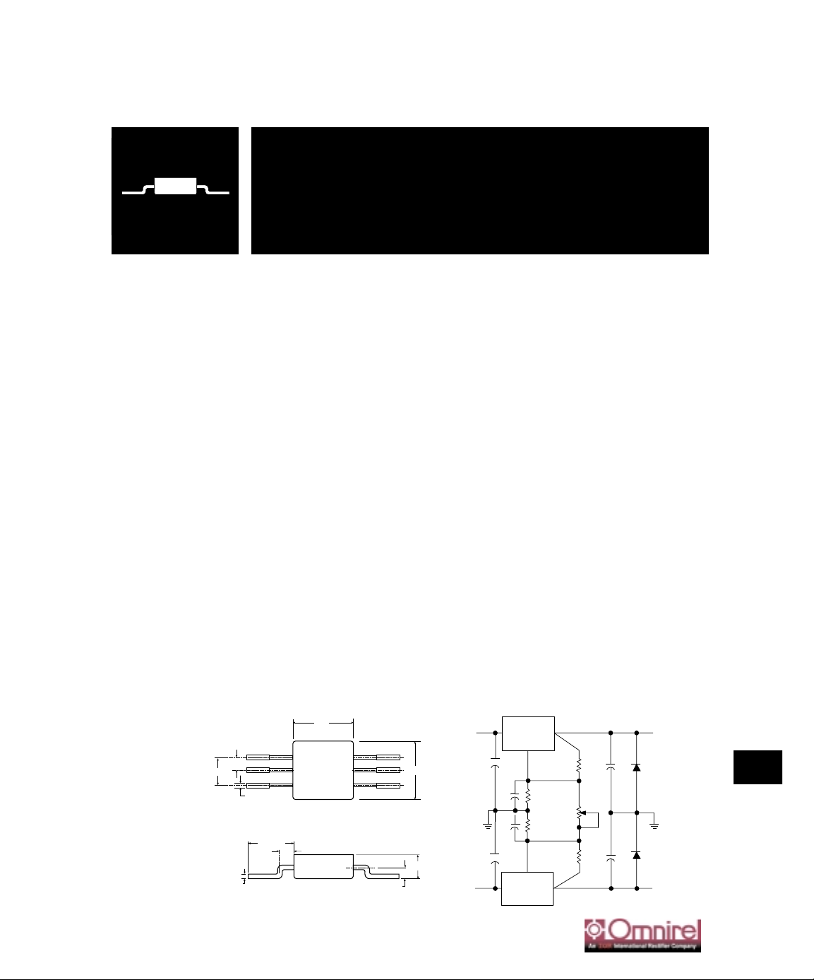
This device offers a positive and negative adjustable regulator in one hermetically sealed 6-pin
surface mount package. All protective features are designed into the circuit, including thermal
shutdown, current limiting, and safe-area control. With heat sinking, these devices can deliver
up to 1.5 amps of output current. This device is ideally suited for military applications where
small size and high reliability is required.
ABSOLUTE MAXIMUM RATINGS
Input - Output Voltage Differential - LT117AHV Positive Regulator ................. +60 V
Input - Output Voltage Differential - LT137AHV Negative Regulator ..................-50 V
Power Dissipation (P
d
) (Internally Limited).........................................20 W
Operating Junction Temperature Range ...............................- 55°C to + 150°C
Storage Temperature Range .........................................- 65°C to + 150°C
Lead Temperature (Soldering 10 seconds) .......................................300°C
Thermal Resistance:
θ
JC
......................................................................4.2°C/W
θ
JA
......................................................................42°C/W
Maximum Output Current .......................................................1.5 A
OM7654SM
DUAL TRACKING SUPPLY ±1.25V TO ±20V
D1
IN4002
POS REG.
V
INVOUT
Adj
Adj
V
INVOUT
NEG REG.
+V
IN
+V
OUT
-V
IN
-V
OUT
R
2
5K
1%
R
4
5k
1%
R
1
**
100Ω
1%
2.2*
µF
1µF*
D2
IN4002
1µF*
10µF
10µF
* Solid Tantalum
** R
1
or R2may be trimmed slightly to improve tracking.
R
3
5K
R
5
**
100Ω
1%
+
+
2.2*
µF
MECHANICAL OUTLINE
.425I
.200I
I
I
.100I
I
.035 WIDEI
FLAT 6 PLCS.I
I
.350 MIN.I
.080 I
I
.160I
.020I
± .020I
.115I
.425I
Pin 1: +V
IN
Pin 2: -V
ADJ
Pin 3: -V
IN
Pin 4: -V
OUT
Pin 5: +V
ADJ
Pin 6: +V
OUT
NOTES:
• Case is metal/hermetically sealed
• Isolated Tab
•
1
2
3
6
5
4
3.5 - 152
OM7645SM
3.5
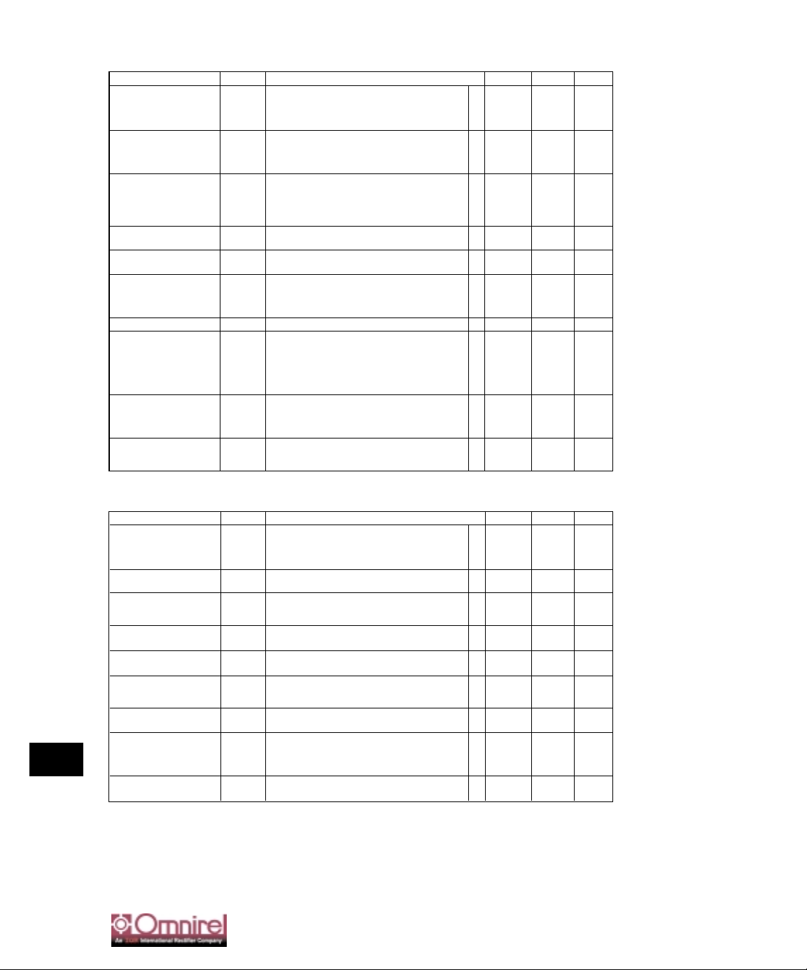
ELECTRICAL CHARACTERISTICS Positive Regulator-55°C ≤ TA≤ 125°C, IL= 8mA (unless otherwise specified)
Parameter Symbol Test Conditions Min. Max. Unit
Reference Voltage V
REF
V
DIFF
= 3.0V, TA= 25°C 1.238 1.262
V
DIFF
= 3.3V • 1.225 1.270 V
V
DIFF
= 40V • 1.225 1.270
V
DIFF
= 60V • 1.225 1.270
Line Regulation R
LINE
3.0V ≤ V
DIFF
≤ 40V, V
out
= V
ref
, TA= 25°C -4.5 4.5
(Note 1) 3.3V ≤ V
DIFF
≤ 40V, V
out
= V
ref
• -9 -9 mV
40V ≤ V
DIFF
≤ 60V, V
out
= V
ref
, TA= 25°C -5 5
40V ≤ V
DIFF
≤ 60V, V
out
= V
ref
• -10 10
Load Regulation R
LOAD
V
DIFF
= 3.0V, 10mA ≤ IL≤ 1.5A, TA= 25°C -15 15
(Note 1) V
DIFF
= 3.3V, 10mA ≤ IL≤ 1.5A • -15 15 mV
V
DIFF
= 40V, 10mA ≤ IL≤ 300mA, TA= 25°C -15 15
V
DIFF
= 40V, 10mA ≤ IL≤ 195mA • -15 15
V
DIFF
= 60V, 10mA ≤ IL≤ 30mA • -15 15
Thermal Regulation V
RTH
Vin= 14.6V, IL= 1.5A -5 5 mV
P
d
= 20 Watts, t = 20 ms, TA= 25°C
Ripple Rejection R
N
f = 120 Hz, V
out
= V
ref
• 66 dB
(Note 2) C
Adj
= 10 µF, I
out
= 100 mA
Adjustment Pin Current I
Adj
V
DIFF
= 3.0V, TA= 25°C 100
V
DIFF
= 3.3V • 100 µA
V
DIFF
= 40V • 100
V
DIFF
= 60V • 100
Adjustment Pin ∆I
Adj
V
DIFF
= 3.0V, 10mA ≤ IL≤ 1.5A, TA= 25°C -5 5
Current Change V
DIFF
= 3.3V, 10mA ≤ IL≤ 1.5A • -5 5
V
DIFF
= 40V, 10mA ≤ IL≤ 300mA, TA= 25°C -5 5
V
DIFF
= 40V, 10mA ≤ IL≤ 195mA • -5 5 µA
3.0V ≤ V
DIFF
≤ 40V, TA= 25°C -5 5
3.3V ≤ V
DIFF
≤ 40V • -5 5
3.3V ≤ V
DIFF
≤ 60V • -5 5
Miminum Load Current I
Lmin
V
DIFF
= 3.0V, V
out
= 1.4V (forced) 5.0
V
DIFF
= 3.3V, V
out
= 1.4V (forced) • 5.0 mA
V
DIFF
= 40V, V
out
= 1.4V (forced) • 5.0
V
DIFF
= 60V, V
out
= 1.4V (forced) • 7.0
Current Limit I
CL
V
DIFF
= 5V • 1.5 3.5
(Note 2) V
DIFF
= 40V, TA= 25°C 0.3 1.5 A
V
DIFF
= 60V, TA= 25°C 0.05 0.50
ELECTRICAL CHARACTERISTICS Positive Regulator-55°C ≤ TA≤ 125°C, IL= 8mA (unless otherwise specified)
Parameter Symbol Test Conditions Min. Max. Unit
Reference Voltage V
REF
V
DIFF
= 3.0V, TA= 25°C -1.262 -1.238
V
DIFF
= 3.0V • -1.28 -1.22 V
V
DIFF
= 50V, TA= 25°C -1.28 -1.22
V
DIFF
= 50V • -1.28 -1.22
Line Regulation R
LINE
3.0 V ≤V
DIFF
≤ 50V, TA= 25°C -6 6
(Note 1)
• -20 20 mV
Load Regulation R
LOAD
V
DIFF
= 50V, 8mA ≤ IL≤110mA, TA= 25°C -25 25
(Note 1) V
DIFF
= 5V, 8mA ≤ IL≤ 1.5A, TA= 25°C -25 25 mV
• -50 50
Thermal Regulation V
RTH
Vin= -14.6V, IL= 1.5A -5 5 mV
P
d
= 20 Watts, t = 10 ms, TA= 25°C
Ripple Rejection R
N
f = 120 Hz, V
out
= V
ref
• 66 dB
(Note 2) C
Adj
= 10 µF, I
out
= 100 mA
Adjustment Pin Current I
Adj
V
DIFF
= 3.0V • 100
V
DIF
= 40V • 100 µA
V
DIFF
= 50V • 100
Adjustment Pin ∆I
Adj
V
DIFF
= 5V, 8mA ≤ I
out
≤ 1.5A • -5 5 µA
Current Change 3V ≤V
DIFF
≤ 50V, IL≤ 8mA • -6 6
Miminum Load Current I
Lmin
V
DIFF
= 3.0V, V
out
= -1.4V (forced) • 3.0
V
DIFF
= 10V, V
out
= -1.4V (forced) • 3.0 mA
V
DIFF
= 40V, V
ou
t = -1.4V (forced) • 5.0
V
DIFF
= 50V, V
out
= -1.4V (forced) • 5.0
Current Limit I
CL
V
DIFF
= 5V • 1.5 3.5
(Note 2) V
DIFF
= 50V, TA= 25°C 0.2 1.0 A
Notes for both Positive and Negative Regulators Characteristics:
1. Load and Line Regulation are specified at a constant junction temperature. Pulse testing with low duty cycle is used
Changes in output voltage due to heating effects must be taken into account separately.
2. If not tested, shall be guaranteed to the specified limits.
3. The
•denotes the specifications which apply over the full operating temperature range.

3.5 - 153
OM7654SM
3.5
0.4
0.2
0
-0.2
-0.4
-0.6
-0.8
-1.0
-75 -50 -25 0 25 50 75 100 125 150
ADJUSTMENT PIN CURRENT
TJ, Junction Temperature (C°)
70
65
60
55
50
45
40
-75 -50 -25 0 25 50 75 100 125 150
TEMPERATURE STABILITY
-75 -50 -25 0 25 50 75 100 125 150
T
J
, Junction Temperature (C°)
1.260
1.250
1.240
1.230
1.220
CURRENT LIMIT
TJ= 25°C
TJ= 55°C
TJ= 150°C
4
3
2
1
0
010203040
VI- VO, Input - Output Voltage Differential (Vdc)
DROPOUT VOLTAGE
IL= 1.5A
∆VO= 100mV
IL= 20mA
IL= 1.0A
IL= 500mA
IL= 200mA
-75 -50 -25 0 25 50 75 100 125 150
TJ, Junction Temperature (C°)
3.0
2.5
2.0
1.5
1.0
MINIMUM OPERATING CURRENT
TJ= 25°C
TJ= 55°C
TJ= 150°C
5.0
4.5
4.0
3.5
3.0
2.5
2.0
1.5
1.0
0.5
0
010203040
V
I
- VO, Input - Output Voltage Differential (Vdc)
POSITIVE REGULATOR - TYPICAL PERFORMANCE CHARACTERISTICS
Positive
Regulator
V
in
Cin*
0.1 µF
V
out
Co**
1.0 µF
R
2
Adjust
I
Adj
R
1
240Ω
STANDARD APPLICATION
*Cinis required if regulator is located an
appreciable distance from power supply filter.
** C
o
is not needed for stability, however it does
improve transient response.
V
out
= 1.25 V (1 + )+ I
Ad j R2
Since I
Adj
is controlled to less than 100 µA,
the error associated with this term is negligible
in most applications.
R
2
R
1
LOAD REGULATION
TJ, Junction Temperature (C°)
IL= 0.5A
VI= 15V
VO= 10V
IL= 1.5A
∆V
O
, Output Voltage Change (%)
I
O
, Output Current (A)
I
Adj
, Adjustment Pin Current (µA)V
ref
, Reference Voltage (V)
I
B
, Quiescent Current (mA) V
I
- V
O
, Input - Output Voltage Differential (V
dc
)
0.4
0.2
0
-0.2
-0.4
-0.6
-0.8
-1.0
-75 -50
0255075
-25
70
65
60
55
50
45
40
35
-75 -50
0255075
-25
1.260
1.250
1.240
1.230
1.220
-75
-50 -25 0 25 50
75
4
3
2
1
0
100
150
125
0
10
20
30
40
3.0
2.5
2.0
1.5
100
150
125
1.0
-75 -50 -25 0
25 50 75
125
100
150
5.0
100
125 150
4.5
4.0
3.5
3.0
2.5
2.0
1.5
1.0
0.5
0
0
10
20 30
40

OM7654SM
3.5
LOAD REGULATION
TJ, Junction Temperature (C°)
IL= 0.5A
IL= 1.5A
VI= -15V
V
O
= -10V
0.2
0
-0.2
-0.4
-0.6
-0.8
-1.0
-1.2
-1.4
-75-50 -25 0 25 50 75 100 125 150
ADJUSTMENT PIN CURRENT
TJ, Junction Temperature (C°)
80
75
70
65
60
55
50
45
40
-75 -50 -25 0 25 50 75 100 125 150
TEMPERATURE STABILITY
TJ, Junction Temperature (C°)
1.270
1.260
1.250
1.240
1.230
-75-50 -25 0 25 50 75 100 125 150
CURRENT LIMIT
VI- VO, Input - Output Voltage Differential (Vdc)
TJ= -25°C
TJ= -55°C
TJ= -150°C
4
3
2
1
0
010203040
DROPOUT VOLTAGE
TJ, Junction Temperature (C°)
IL= 1.5A
VO= -5V
∆VO= 100mV
IL= 20mA
IL= 1.0A
IL= 500mA
IL= 200mA
3.0
2.5
2.0
1.5
1.0
-50 -25 0 25 50 75 100 125 150
MINIMUM OPERATING CURRENT
TJ= 25°C
TJ= -55°C
TJ= 150°C
1.8
1.6
1.4
1.2
1.0
0.8
0.6
0.4
0.2
0
010203040
VI- VO, Input - Output Voltage Differential (Vdc)
NEGATIVE REGULATOR - TYPICAL PERFORMANCE CHARACTERISTICS
V
ref
, Reference Voltage (V)
∆V
O
, Output Voltage Change (%)
I
O
, Output Current (A)
I
Adj
, Adjustment Pin Current (µA)
V
I
- V
O
, Input - Output Voltage Differential (V
dc
)I
B
, Quiescent Current (mA)
Negative
Regulator
1.0µF
1.0µF
-V
IN
-V
OUT
V
OUT
V
IN
I
Adj
I
PROG
CIN*C
O
**
R
2
R
1
120Ω
++
STANDARD APPLICATION
*Cinis required if regulator is located an
appreciable distance from power supply filter.
** Cois not needed for stability, however it does
improve transient response.
V
out
= -1.25 V (1 + )+ I
Ad j R2
Since I
Adj
is controlled to less than 100 µA,
the error associated with this term is negligible
in most applications.
R
2
R
1
0.2
0
-0.2
-0.4
-0.6
-0.8
-1.0
-1.2
-1.4
-50 -25
0255075 100
80
75
70
65
60
55
50
45
40
-50 -25 0
25 50 75 100
1.270
1.260
1.250
1.240
1.230
-50 -25 0 25 50 75 100 125 150
125
125
150
150
4
3
2
1
0
0
10
20
3.0
2.5
2.0
1.5
1.0
-50
0255075 100
-25
1.8
1.6
1.4
1.2
1.0
0.8
0.6
0.4
0.2
0
0
10 20 30
30 40
125 150
40
 Loading...