

OLYMPUS C-960 Zoom Description of Mechanism V2

H. DESCRIPTION OF MECHANISM
H. DESCRIPTION OF MECHANISM
[1] CA1 CIRCUIT DESCRIPTION ................................................................................ H-2
[2] ST1 POWER CIRCUIT DESCRIPTION ..................................................................H-7
[3] ST1 FLASH CIRCUIT DESCRIPTION .................................................................... H-8
[4] SY1 CIRCUIT DESCRIPTION ................................................................................. H-9
SERVER_DIS
H-1 Ver.2
H. DESCRIPTION OF MECHANISM
[ 1 ] CA1 CIRCUIT DESCRIPTION
1. IC Configuration
IC903 (RJ23J1AB0AT) CCD imager
IC902 (74VHC04MTC) H driver
IC904 (LR366854) V driver
IC905 (AD9802) CDS, AGC, A/D converter
1B
φ
φ
V
V
GND
VOUT
7
8
6
4
5
φ
φ
V
V
3
2
3B
2
1A
4
3A
φ
φ
V
V
1
2. IC903 (CCD)
[Structure]
Interline type CCD image sensor
Optical size 1/2.7 inch format
Effective pixels 1292 (H) x 966 (V)
Pixels in total 1344 (H) x 971 (V)
Optical black
Horizontal (H) direction: Front 3 pixels, Rear 49 pixels
Vertical (V) direction: Front 2 pixels, Rear 3 pixels
Dummy bit number Horizontal : 28 Vertical : 2
Pin 1
2
V
3
3
Pin 9
Fig. 1-1.Optical Black Location (Top View)
H
49
Ye
G
Ye
G
Ye
Vertical register
G
Horizontal register
11
SUB
φ
12
SUB
C
9
10
DD
V
GND
Fig. 1-2. CCD Block Diagram
Cy
Ye
Cy
Mg
Cy
Mg
Cy
Mg
13
G
Mg
Ye
Cy
G
Mg
Ye
Cy
G
Mg
(Note)
14
15
RG
φ
1
φ
H
L
V
(Note): Photo sensor
16
2
φ
H
Pin No.
1
2, 3
4
5, 6
7, 10
8
9
11
12
13
14
15
16
Symbol
V
φ
V
3B, Vφ3A
V
φ
V
1B, Vφ1A
GND
OUT
V
VDD
φ
SUB
VL
φ
RG
OSUB
H
H
Pin Description
φ
Vertical register transfer clock
4
Vertical register transfer clock
φ
Vertical register transfer clock
2
Vertical register transfer clock
GND
Signal output
Circuit power
Substrate clock
Protection transistor bias
Reset gate clock
Reset gate clock DC
φ
Horizontal register transfer clock
1
φ
Horizontal register transfer clock
2
Table 1-1. CCD Pin Description
Waveform
GND
DC
DC
DC
Voltage
-7 V, 0 V
-7 V, 0 V, 13 V
-7 V, 0 V
-7 V, 0 V, 13 V
0 V
Aprox. 6 V
13 V
Aprox. 6 V
(Different from every CCD)
-7V
8 V, 11.5 V
Aprox. 9 V
(Different from every CCD)
0 V, 3.5 V
0 V, 3.5 V
When sensor read-out
SERVER_DIS
H-2 Ver.2
H. DESCRIPTION OF MECHANISM
27
29
36
26
16
22
21
30
2319
11
12
17
PBLK
A/D
ACVDD
CMLEVEL
VRT
VTB
STBYCLPOB
ADCMODE
TIMING
GENERATOR
CLPDM PGACONT1
PGACONT2
SHP
SHD ADCCLK
PIN
DIN
ADCIN
DOUT
DRVDD
DVDD
ADVDD
2
37 20
18
47
48
43
3341
CLAMP
REFERENCE
CLAMP
CDS
PGA
MUX S/H
AD9802
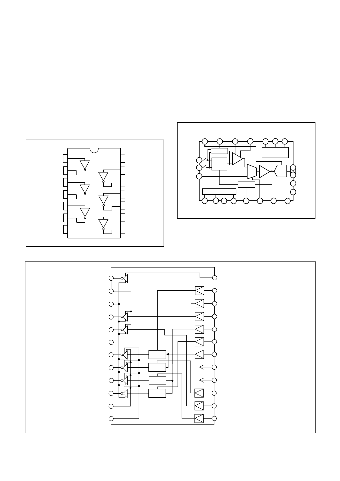
3. IC902 (H Driver) and IC904 (V Driver)
An H driver (IC902) and V driver (IC904) are necessary in
order to generate the clocks (vertical transfer clock, horizontal transfer clock and electronic shutter clock) which driver
the CCD.
IC902 is an inverter IC which drives the horizontal CCDs
(H1 and H2). In addition the XV1-XV4 signals which are output from IC102 are the vertical transfer clocks, and the XSG1
and XSG signal which is output from IC102 is superimposed onto XV1 and XV3 at IC904 in order to generate a
ternary pulse. In addition, the XSUB signal which is output
from IC102 is used as the sweep pulse for the electronic
shutter, and the RG signal which is output from IC102 is the
reset gate clock.
14
CC
1A
1Y
2A
2Y
1
2
3
4
V
13
6A
12
6Y
11
5A
4. IC905 (CDS, AGC Circuit and A/D Converter)
The video signal which is output from the CCD is input to
Pins (26) and (27) of IC905. There are S/H blocks inside
IC905 generated from the XSHP and XSHD pulses, and it is
here that CDS (correlated double sampling) is carried out.
After passing through the CDS circuit, the signal passes
through the AGC amplifier. It is A/C converted internally into
a 10-bit signal, and is then input to IC102 of the CA2 circuit
board. The gain of the AGC amplifier is controlled by the
voltage at pin (29) which is output from IC102 of the CA2
circuit board and smoothed by the PWM.
5
3A
6
3Y
7
GND
Fig. 1-3. IC902 Block Diagram
VSHT
VMb
VL
V2
V4
NC
V3B
V3A
10
5Y
4A
9
4Y
8
1
2
3
4
5
6
7
8
MIX
MIX
Fig. 1-5. IC905 Block Diagram
24
VOFDH
XSG2B
23
XSUB
22
XV2
21
20
XV1
19
XSG1A
XV3
18
VDD
17
Ver.2
V1B
V1A
VMa
VH
10
11
12
9
MIX
MIX
Fig. 1-4. IC904 Block Diagram
H-3
16
15
14
13
GND
XSG2A
XV4
XSG1B
SERVER_DIS
H. DESCRIPTION OF MECHANISM
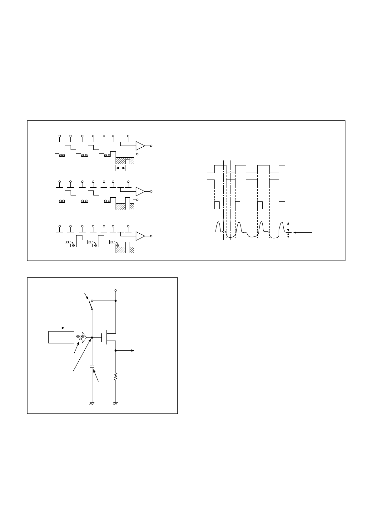
5. Transfer of Electric Charge by the Horizontal CCD
The transfer system for the horizontal CCD emplays a 2-phase drive method.
The electric charges sent to the final stage of the horizontal CCD are transferred to the floating diffusion, as shown in Fig. 1-
6. RG is turned on by the timing in (1), and the floating diffusion is charged to the potential of PD. The RG is turned off by the
timing in (2). In this condition, the floating diffusion is floated at high impedance. The H1 potential becomes shallow by the
timing in (3), and the electric charge now moves to the floating diffusion.
Here, the electric charges are converted into voltages at the rate of V = Q/C by the equivalent capacitance C of the floating
diffusion. RG is then turned on again by the timing in (1) when the H1 potential becomes deep.
Thus, the potential of the floating diffusion changes in proportion to the quantity of transferred electric charge, and becomes
CCD output after being received by the source follower. The equivalent circuit for the output circuit is shown in Fig. 1-7.
(1)
H1 H2 H1 H2 H1 HOG RG
CCD OUT
Floating diffusion
(2)
H1 H2 H1 H2 H1 HOG RG
PD
PD
CCD OUT
H1
H2
RG
15.5V
(1) (2) (3)
3.5V
0V
3.5V
0V
12V
(3)
H1 H2 H1 H2 H1 HOG RG
Fig. 1-6. Horizontal Transfer of CCD Imager and Extraction of Signal Voltage
Reset gate pulse
Direction of transfer
H Register
Electric
charge
Floating diffusion gate is
floated at a high impedance.
C is charged
equivalently
13V Pre-charge drain bias (PD)
Voltage output
Fig. 1-7. Theory of Signal Extraction Operation
CCD OUT
CCD OUT
RG pulse peak signal
Signal voltage
Detection of the standard zoom positions is carried out by
means of the two photoreflectors (PR1 and PR2) inside the
lens block.
6-2. Focus drive
The four control signals (LDIN1, LDIN2, LDIN3 and LDIN4)
with different phases which are output from the ASIC expansion port (IC107) are converted into drive pulses (LDOUT1,
LDOUT2, LDOUT3 and LDOUT4) by the motor driver (IC954),
and are then used to drive the stepping motor for focusing
operation. Detection of the standard focusing positions is
carried out by means of the photointerruptor (PI) inside the
lens block.
6-3. Iris drive
The two control signals (ACTRL1 and ACTRL2) which are
output from the ASIC expansion port (IC106) are converted
into drive pulses by the motor driver (IC957), and are then
used to drive the iris motor.
Black level
6. Lens drive block
6-1. Zoom drive
The four control signals (ZIN1, ZIN2, ZIN3 and ZIN4) with
different phases which are output from the ASIC expansion
port (IC107) are converted into drive pulses (ZOOM1, ZOOM2,
ZOOM3 and ZOOM4) by the motor drive (IC953), and are then
used to drive the stepping motor for zoom operation.
SERVER_DIS
6-4. Shutter drive
The control signal (PCTRL) which is output from the ASIC
expansion port (IC106) is converted into a drive pulse by the
transistor (Q9501), and is then used to drive the shutter
plunger. The drive current is maintained at a constant level by
IC952 and Q9501.
H-4 Ver.2
 Loading...