

Page 1

H. DESCRIPTION OF MECHANISM
C-8080Wide Zoom
H. DESCRIPTION OF MECHANISM
[1] CA1 CIRCUIT DESCRIPTION ................................................................................ H-2
[2] CP1 CIRCUIT DESCRIPTION ................................................................................ H-4
[3] PW1 POWER CIRCUIT DESCRIPTION ................................................................. H-5
[4] ST1 STROBE CIRCUIT DESCRIPTION................................................................. H-6
[5] SYA CIRCUIT DESCRIPTION................................................................................. H-7
H-1 Ver.1
Page 2
H. DESCRIPTION OF MECHANISM C-8080Wide Zoom
2
8
1
D
[1] CA1 CIRCUIT DESCRIPTION
1. IC Configuration
IC903 (ICX456AQ) CCD imager
IC904 (AD9945) CDS, AGC, A/D converter
IC905 (CXD3622GA) TG
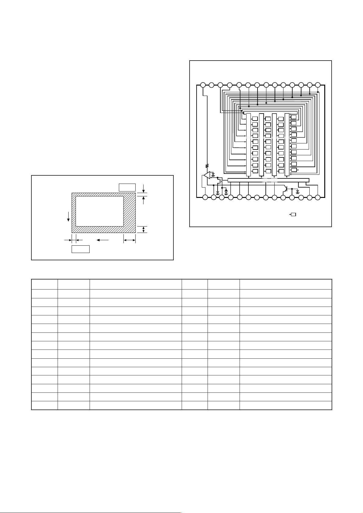
2. IC903 (CCD)
[Structure]
Interline type CCD image sensor
Optical size Diagonal 11 mm (2/3 type)
Effective pixels 3280 (H) x 2454 (V)
Pixels in total 3350 (H) x 2482 (V)
Optical black
Horizontal (H) direction: Front 12 pixels, Rear 50 pixels
Vertical (V) direction: Front 8 pixels, Rear 2 pixels
Pin 1
V
14
GND
OUT
V
13
GND
1615
Ø1B
V
Ø1
LH
V
10
19
Ø1C
H
Ø2
V
V
8
9
Gb
R
Gb
R
Gb
R
Gb
Vertical register
R
Gb
R
Horizontal register
20
21
Ø2C
GND
H
7
6
B
Gr
B
Gr
B
Gr
B
Gr
B
Gr
23
22
Ø1B
H
(Note) : Photo sensor
Ø1A
V
12
11
1817
DD
RG
V
Ø
V
Ø2B
H
Ø5B
Ø5A
V
V
3
4
5
B
Gb
Gr
R
B
Gb
Gr
R
B
Gb
Gr
R
B
Gb
Gr
R
B
Gb
Gr
R
(Note)
25
26
24
SUB
SUB
C
Ø
Ø4
Ø3AVØ3B
Ø1C
ØHL
Ø6
ØST
V
V
V
1
2
28
27
L
V
Ø2A
Ø1A
H
H
2
Pin 15
H
Fig. 1-1.Optical Black Location (Top View)
Pin No.
1
2
3
4
5
6
7
8
9
10
11
12
13
14
Symbol
Vφ
HLD
VφST
Vφ6
Vφ5B
Vφ5A
Vφ4
Vφ3B
Vφ3A
Vφ2
Vφ1C
Vφ
1B
1A
Vφ
GND
GND
Horizontal addition control clock
Horizontal addition control clock
Vertical register transfer clock
Vertical register transfer clock
Vertical register transfer clock
Vertical register transfer clock
Vertical register transfer clock
Vertical register transfer clock
Vertical register transfer clock
Vertical register transfer clock
Vertical register transfer clock
Vertical register transfer clock
GND
GND
Pin Description
50
Pin No.
15
16
17
18
19
20
21
22
23
24
25
26
27
28
Fig. 1-2. CCD Block Diagram
Symbol
OUT
V
VDD
φRG
LHφ
1
Hφ1C
Hφ2C
GND
Hφ
1B Horizontal register transfer clock
2B
Hφ
φSUB
C
SUB
V
L
1A
Hφ
Hφ2A
Signal output
Circuit power
Reset gate clock
Horizontal register last step transfer clock
Horizontal register transfer clock
Horizontal register transfer clock
GND
Horizontal register transfer clock
Substrate clock
Substrate bias
Protection transistor bias
Horizontal register transfer clock
Horizontal register transfer clock
Pin Description
Table 1-1. CCD Pin Description
H-2 Ver. 1
Page 3
H. DESCRIPTION OF MECHANISMC-8080Wide Zoom
C
B
D
S
3. IC905 (TG)
IC905 is timing generator for image sensor. This is equipped
with H driver and V driver.
4. IC904 (CDS, AGC and A/D converter)
IC904 contains the functions of CDS, AGC and A/D converter.
The video signal which is output from the CCD is input to
pins (22) of IC904. There are sample hold blocks inside
IC904 generated from the SHP and SHD pulses, and it is
here that CDS (correlated double sampling) is carried out.
After passing through the CDS circuit, the signal passes
through the AGC amplifier (PGA: Programmable Gain Amplifier). It is A/D converted internally into a 12-bit signal,
and is then input to ASIC (IC102). The gain of the AGC
amplifier is controlled by pin (25)-(27) serial signal which is
output from ASIC (IC102).
PBLK
VRB
VRT
DRVD
DRVS
12
DOUT
CDIN
AD9945
CDS
6~40 dB
VGA
BANDGAP
REFERENCE
12-BIT
ADC
+
AVDD
AVSS
8
CLP
BLK LEVEL
OFFSET
INTERNAL
TIMING
SHP
SHD
10
CONTROL
REGISTERS
DIGITAL
INTERFACE
SL
SCK
SDATA
Fig. 1-3. IC904 Block Diagram
DATACLK
CLPO
DVDD
DVSS
H-3 Ver. 1
Page 4

H. DESCRIPTION OF MECHANISM C-8080Wide Zoom
[2] CP1 CIRCUIT DESCRIPTION
1. Circuit description
1-1. Signal processor
γγ
1.
γ correction circuit
γγ
This circuit performs (gamma) correction in order to maintain a linear relationship between the light input to the camera and the light output from the picture screen.
2. Color generation circuit
This circuit converts the CCD data into RGB signals.
3. Matrix circuit
This circuit generates the Y signals, R-Y signals and B-Y
signals from the RGB signals.
4. Horizontal and vertical aperture circuit
This circuit is used gemerate the aperture signal.
1-2. AE/AWB and AF computing circuit
The AE/AWB carries out computation based on a 64-segment screen, and the AF carries out computations based
on a 6-segment screen.
1-3. SDRAM controller
This circuit outputs address, RAS, CAS and AS data for
controlling the SDRAM. It also refreshes the SDRAM.
After AWB and
erated and aperture correction is carried out for the Y signal, and the data is then compressed by JPEG and is then
written to card memory (xD picture card).
When the data is to be output to an external device, it is
taken data from the memory. When played back on the LCD
and monitor, data is transferred from memery to the SDRAM,
and the image is then elongated so that it is displayed over
the SDRAM display area.
γγ
γ processing are carried out, a matrix is gen-
γγ
3. LCD Block
LCD Block is in the CP1 board, and it is constructed by
LCD driver (IC871) and around circuits.
The video signal from the ASIC are converted into RGB
signals by the LCD driver, and these RGB signals and the
control signal which is output by the LCD driver are used to
drive the LCD panel. The RGB signals are 1H transposed
so that no DC component is present in the LCD element,
and the two horizontal shift register clocks drive the horizontal shift registers inside the LCD panel so that the 1H
transposed RGB signals are applied to the LCD panel. Because the LCD closes more as the difference in potential
between the COM (common polar voltage: AC) and the R,
G and B signals becomes greater, the display becomes
darker; if the difference in potential is smaller, the element
opens and the LCD become brighter.
1-4. SIO
This is the interface for the 8-bit microprocessor.
1-5. PIO/PWM/SIO for LCD
8-bit parallel input and output makes it possible to switch
between individual input/output and PWM input/output.
1-6. TG/SG
Timing generated for 8 million pixel CCD control.
1-7. Digital encorder
It generates chroma signal from color difference signal.
2. Outline of Operation
When the shutter opens, the reset signals (ASIC and CPU)
and the serial signals (take a picture commands) from the
8-bit microprocessor are input and operation starts. When
the TG/SG drives the CCD, picture data passes through
the A/D and CDS, and is then input to the ASIC as 12-bit
data.
The AF, AE, AWB, shutter, and AGC value are computed
from this data, and three exposures are made to obtain the
optimum picture. The data which has already been
stored in the SDRAM is read by the CPU and color generation is carried out. At this time, correction of the lens distortion which is a characteristic of wide-angle lenses is carried
out.
4. Lens drive block
4-1. Shutter drive
The shutter drive signal (SIN1, SIN2) which is output from
the ASIC (IC101) is drived the shutter constant level driver,
and then shutter plunger is opened and closed.
4-2. Iris drive
The iris stepping motor drive signals (ACTRL1, ACTRL2,
ACTRL3 and ACTRL4) which are output from the ASIC
(IC101) are used to drive by the motor driver (IC956). Detection of the standard iris positions is carried out by means
of the standard switch (HSW) inside the lens block.
4-3. Focus drive
The focus stepping motor drive signals (FIN1, FIN2, FIN3
and FIN4) which are output from the ASIC (IC101) are used
to drive by the motor driver (IC956). Detection of the standard focusing positions is carried out by means of the
photointerruptor (PI) inside the lens block.
4-4. Zoom drive
The zoom DC motor drive signals (ZIN1, ZIN2) which are
output from the ASIC (IC101) are used to drive by the motor
driver (IC956). Detection of the zoom standard positions is
carried out by means of standard switch (WSW) inside the
lens block. Also counting of the zoom positions is carried out
by means of photointerruptor (ZPULSE) inside the lens block.
H-4
Ver. 1
Page 5

H. DESCRIPTION OF MECHANISMC-8080Wide Zoom
[3] PW1 POWER CIRCUIT DESCRIPTION
1. Outline
This is the main power circuit, and is comprised of the following blocks.
Switching power controller (IC501)
Strobo system power output and analog system power output (T5001, Q5001)
Digital 1.7 V power supply output (Q5013, L5006)
Digital 3.25 V power supply output (Q5014, L5007)
LCD system power supply output (Q5015, L5008)
Backlight power supply output (Q5018, L5009)
AF LED power supply output (Q5033, L5016)
2. Switching Power Controller (IC501)
This is the basic circuit which is necessary for controlling
the power supply for a PWM-type switching regulator, and
is provided with six built-in channels, only CH1 (strobo system power output, analog system power output), CH2 (digital
1.7 V power supply output), CH3 (digital 3.25 V power supply output), CH4 (LCD system power supply output), CH5
(backlight power supply output) and CH6 (AF LED power
supply output) are used. Feedback from 15 V (A) (CH1),
1.7 V (D) (CH2), 3.25 V (D) (CH3), 12.0 V (L) (CH4) and AF
LED V (CH6) power supply outputs are received, and the
PWM duty is varied so that each one is maintained at the
correct voltage setting level.
Feedback for the LCD backlight power (CH5) is provided to
the both ends voltage of registance so that regular current
can be controlled to be current that was setting.
2-1. Short-circuit protection circuit
If output is short-circuited for the length of time determined
by the condenser which is connected to Pin (37) of IC501,
all output is turned off. The control signal (P ON) are recontrolled to restore output.
3. Strobo System 15 V and Analog System Power
Output
15 V (F), 15.0 V (A) and -7.6 V (A) are output. Feedback for
the 15 V (A) is provided to the switching controller (Pin (40)
of IC501) so that PWM control can be carried out.
4. Digital 1.7 V System Power Output
1.7 V (D) is output. Feedback for the 1.7 V (D) is provided to
the swiching controller (Pin (43) of IC501) so that PWM
control can be carried out.
5. Digital 3.25 V System Power Output
3.25 V (D) is output. Feedback for the 3.35 V (D) is pro-
vided to the swiching controller (Pin (45) of IC501) so that
PWM control can be carried out.
6. LCD System Power Output
12.0 V (L) is output. Feedback for the 12.0 V (L) is provided
to the switching power controller (Pin (47) of IC501) so that
PWM control can be carried out.
7. Backlight Power Output
Regular current (15 mA) is being transmitted to LED for
LCD backlight. Feedback for the both ends voltage of
registance that is being positioned to in series LED are provided to the switching controller (Pin (2) of IC501) so that
PWM control to be carried out.
8. AF LED Power Output
AF LED V (7V) is output. Feedback for the AF LED V is
provided to the switching power controller (Pin (4) of IC501)
so that PWM control can be carried out.
9. Analog System (3.45 V) Power Output
3.45 V (A) is output. Feedback for the 3.45 V (A) is provided
to the switching power controller (Pin (5) of IC502) so that
PWM control can be carried out.
H-5 Ver. 1
Page 6

H. DESCRIPTION OF MECHANISM C-8080Wide Zoom
[4] ST1 STROBE CIRCUIT DESCRIPTION
1. Charging Circuit
When UNREG power is supplied to the charge circuit and
the CHG signal from SYA circuit on the CP1 board becomes
High (3.3 V), the charging circuit starts operating and the
main electorolytic capacitor is charged with high-voltage
direct current.
However, when the CHG signal is Low (0 V), the charging
circuit does not operate.
1-1. Power supply filter
C5401 constitutes the power supply filter. They smooth out
ripples in the current which accompany the switching of the
oscillation transformer.
1-2. Oscillation circuit
This circuit generates an AC voltage (pulse) in order to increase the UNREG power supply voltage when drops in
current occur. This circuit generates a drive pulse with a
frequency of approximately 50-100 kHz. Because self-excited light omission is used, the oscillation frequency
changes according to the drive conditions.
1-3. Oscillation transformer
The low-voltage alternating current which is generated by
the oscillation control circuit is converted to a high-voltage
alternating current by the oscillation transformer.
2. Light Emission Circuit
When RDY and TRIG signals are input from the ASIC expansion port, the stroboscope emits light.
2-1. Emission control circuit
When the RDY signal is input to the emission control circuit, Q5409 switches on and preparation is made to let current flow to the light emitting element. Moreover, when a
STOP signal is input, the stroboscope stops emitting light.
2-2. Trigger circuit
When a TRIG signal is input to the trigger circuit, D5405
switches on, a high-voltage pulse of several kilovolts is generated inside the trigger circuit, and this pulse is then applied to the light emitting part.
2-3. Light emitting element
When the high-voltage pulse form the trigger circuit is applied to the light emitting part, currnet flows to the light emitting element and light is emitted.
Beware of electric shocks.
1-4. Rectifier circuit (T5401)
The high-voltage alternating current which is generated at
the secondary side of T5401 is rectified to produce a highvoltage direct current and is accumulated at electrolytic capacitor C5412 on the main circuit board.
1-5. Voltage monitoring circuit
This circuit is used to maintain the voltage accumulated at
C5412 at a constance level.
After the charging voltage is divided and converted to a
lower voltage by R5417 and R5419, it is output to the SYA
circuit on the CP1 board as the monitoring voltage VMONIT.
When this VMONIT voltage reaches a specified level at the
SYA circuit on the CP1 board, the CHG signal is switched
to Low and charging is interrupted.
H-6 Ver. 1
Page 7

H. DESCRIPTION OF MECHANISMC-8080Wide Zoom
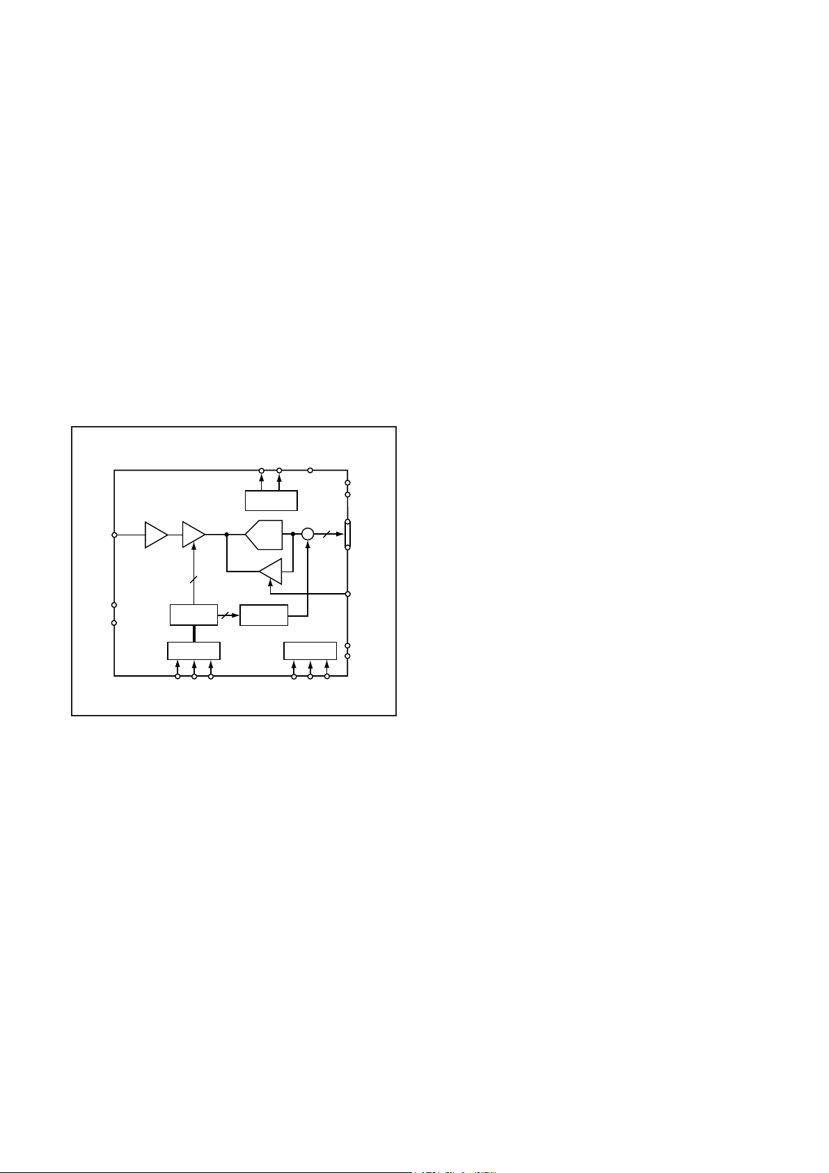
[5] SYA CIRCUIT DESCRIPTION
1. Configuration and Functions
For the overall configuration of the SYA block, refer to the block diagram. The configuration of the SYA block centers around
a 8-bit microprocessor (IC301).
The 8-bit microprocessor handles the following functions.
1. Operation key input, 2. Clock control, 3. Power ON/OFF, 4. Storobe charge control
Pin
1
2
3
4
5
6
7
8
9
10
11
12
13
14
15
16
17
18
19
20
21 ZPULSE
22 LCD ON
23 EVF BL
24
25 SCAN IN3/PRG SO
26
27
28
29
30
31
32
33
34
35
36
37
38
39
40
41~46
Signal
AVR EF
AVSS
IC (FLMD0)
VDD
REGC
VSS
XIN
XOUT
RESET
XCIN
XCOUT
CLKSEL0
BAT_OFF
IR IN
USB CONNECT
EX STROBO
SREQ
COMREQ
JOG A
FLMD1
LCD BL
SCAN IN2/PRG SI
SCAN IN1/PRG SCK
MAIN RESET
SELF_LED
CARD LED
AVREF ON
VSS
VDD
P ON
PA ON
SCK
SI
SO
CHG ON
FLMD0_SY
SCAN OUT 3~0, 4, 5
I/O
O
O
O
O
O
O
I/O
I/O
O
O
O
O
O
O
O
O
O
O
O
Outline
I
-
I
I
-
-
I
I
I
I
I
I
I
I
I
I
I
I
I
-
I
I
Analog standard voltage input terminal
GND
Power for program writing
VDD
Regulator output stability capacity connection
GND
Main clock oscillation terminal (4MHz)
Main clock oscillation terminal
Reset input (L= RESET)
Clock oscillation terminal (32.768 kHz)
Clock oscillation terminal
PLL oscillation ON/OFF (H= ON)
Battery off detection signal input (L= detection)
Remote control detection signal
USB power detection terminal
External strobo connection detection (L= detection)
Serial communication requirement signal
ASIC serial communication requirement
Jog dial A detection
Power for program writing
Zoom motor drive pulse count
D/D converter (LCD system) ON/OFF signal
EVF backlight ON/OFF signal
LCD backlight ON/OFF signal
Key matrix input/Flash for serial data output
Key matrix input/Flash for serial data input
Key matrix input/Flash for serial clock output
System reset (MRST)
Self-timer LED (L = Lighting)
Card LED ON/OFF signal (L = LED lighting)
A/D standard voltage ON/OFF signal (L=ON)
GND
VDD
D/D converter (digital system) ON/OFF signal (H= ON)
D/D converter (analog system) ON/OFF signal (H= ON)
Serial clock output
Serial data input
Serial data output
Strobe charge control (H=ON)
Port for 8-bit rewriting
Key matrix output
H-7
Ver. 1
Page 8

H. DESCRIPTION OF MECHANISM C-8080Wide Zoom
47
48
49
50~53
54
55
56
57
58
59
60
61
62
63
64
PLLEN
ASIC TEST
EVF ON
SCAN IN 6~4, 0
TG RST
USB RST
BACKUP_CTL
CARD SW
JOG B
PAF THERM
xD CARD
CF CARD
SCAN IN 7
CHG VOL
BATTERY
O PLL oscillation ON/OFF (H= ON)
O
O
I
O
O
O
I
I
I
I
I
I
I
I
Table 5-1. 8-bit Microprocessor Port Specification
ASIC control signal (ZTEST)
D/D converter (EVF system) ON/OFF signal (H= ON)
Key matrix input
CCD TG RESET signal
USB RESET signal
Backup battery charge control (L= charge)
Card lid switch detection (L= detection)
Jog dial B detection
Passive sensor temperature detection
xD card detection signal (L= detection)
Expansion memory card (CF) attachement detection signal (L= detection)
Key matrix input
Main capacitor charge voltage detection
Battery voltage detection
2. Internal Communication Bus
The SYA block carries out overall control of camera operation by detecting the input from the keyboard and the condition of
the camera circuits. The 8-bit microprocessor reads the signals from each sensor element as input data and outputs this data
to the camera circuits (ASIC) or to the LCD display device as operation mode setting data. Fig. 5-1 shows the internal
communication between the 8-bit microprocessor and ASIC.
RESET
SREQ
PLL EN
8-bit
Microprocessor
Fig. 5-1 Internal Bus Communication System
ASIC SO
CLKSEL0
ASIC SI
ASIC SCK
ASIC
RESET
H-8
Ver. 1
Page 9

H. DESCRIPTION OF MECHANISMC-8080Wide Zoom
3. Key Operaiton
For details of the key operation, refer to the instruction manual.
SCAN
SCAN
OUT
IN
0
1
2
3
4
0
P
NIGHT
SCENE
1st
PICTURE
QUALITY
WIDE TELE
1
A
LAND-
SCAPE
2nd
WB
23
S
SPORTS
AEL
DC_IN
POP UP
M
PORTRAIT
SELF/REMOTE
CONTROL
EXTRA_
BAT
AV JACK
4
My MOVIE
SETUP
EXPOSURE
CONTROL
UP
CF/XD
5
PLAY
SPOT FLASH
DOWN
OK/MENU
LEFT
Quick View
6
7
AF/MF/
MACRO
RIGHT
5
PW ON
CUSTOM
Table 5-2. Key Operation
TEST
4. Power Supply Control
The 8-bit microprocessor controls the power supply for the overall system.
The following is a description of how the power supply is turned on and off. When the battery is attached, power voltage is
supplied to IC302, a regulated 3.2 V voltage is normally input to the 8-bit microprocessor (IC301) by IC302, clock counting
and key scanning is carried out even when the power switch is turned off, so that the camera can start up again.
When the power switch is off, the 8-bit microprocessor halts 4 MHz of the main clock, and operates 32.768 kHz of subclock.
When the battery is removed, the 8-bit microprocessor power switches the capacitor for memory backup by IC302, and
operates at low consumption. At this condition, the 8-bit microprocessor halts the main clock, and operates clock counting by
sub clock.
Also, the secondary battery for backup is charged 10 hours from it to be attached.
When the power switch is on, the 8-bit microprocessor starts processing. The 8-bit microprocessor first sets both the PON
signal at pin (34) and the PAON signal at pin (35) to High, and then turn on the power circuit. After PON signal is to High, sets
external port of ASIC after approximately 100 ms. According to setting of this external port, carry out setting of the operating
frequency and oscillation control in the ASIC. Also, it starts communication with ASIC, and confirms the system is operative.
When the through image is operating, set the PAON signal to High and then turn on the CCD. When playing, set the PAON
signal to Low and then turn off the CCD. When LCD panel turns on, set LCD ON signal at pin (22) to High, and then turn on
the power. Set LCD BL signal at pin (24) to High, and turn on the backlight power.
When the power switch is off, the lens will be stowed, and PON, PAON, LCDON and LCDBL signals to Low and the power
supply to the whole system is halted. The 8-bit microprocessor halts oscillation of the main clock, and set operation mode of
clock ocillation.
Power supply voltage
Power OFF
Playback mode
Shooting mode (LCD)
Shooting mode (EVF)
Shooting
USB connection
ASIC,
memory
1.7 V, 3.25 V
OFF
ON
ON
ON
ON
ON
Table 5-3. Power supply control
H-9
CCD
15 V, -7.5 V
3.45 V
OFF
OFF
OFF
OFF
ON
OFF
8bit
CPU
3.2 V
32KHz
4MHz
4MHz
4MHz
4MHz
4MHz
LCD
MONITOR
12 V, 3.0 V
OFF
ON
ON
OFF
ON
OFF
Ver. 1
 Loading...