E2E1020-27-Y3
¡ Semiconductor MSM65354/65353A
¡ Semiconductor
This version: Jan. 1998
Previous version: Nov. 1996
MSM65354/65353A
8-Bit Microcontroller with A/D Converter (with LCD Driver)
GENERAL DESCRIPTION
The MSM65354/MSM65353A is a high performance 8-bit microcontroller that employs
OKI original CPU core
byte data memory, LCD driver, A/D converter and shift register. The MSM65353A contains
16K-byte program memory, 384-byte data memory, LCD driver, A/D converter and shift
register. Also available is the MSM65P354, which replace the on-chip program memory with
one-time PROM.
FEATURES
• Operating range
Operating voltage : 2.7V to 5.5V
Operating temperature : –20°C to +70°C
Operating frequency (dual clock)
High speed side : 0 to 10MHz (@V
Low speed side : 32.768kHz (@VDD=2.7V to 5.5V)
Current consumption (Typ.)
High speed side : 5mA (@5MHz, VDD=3V)
Low speed side : 45mA (@32.768kHz, VDD=3V)
• Minimum instruction execution time : 400ns (@10MHz), 800ns (@5MHz)
• CPU core : 8-bit CPU core nX-8/50
• General memory space : 24K-byte program memory + 256-byte data
• Local memory space : 384-byte data memory + SFR
• LCD driver :
• I/O port
Input-output port : 5 ports ¥ 8 bits
Input port : 1 port ¥ 1 bit, 1 port ¥ 8 bits
Output port : 1 port ¥ 1 bit
• Timer : 8-bit auto-reload timer ¥ 3 (one of them can
• Counter : Time base counter ¥ 1 (14 bits)
• Buzzer output circuit : 1 line, selectable from 1000Hz to 16000Hz
• Shift register : 2ch, with 16-byte automatic transfer
• A/D converter : 8ch, 8 bits (4ch of them can start the CPU
nX-8/50. The MSM65354 contains 24K-byte program memory, 640-
=5V±10%)
DD
0 to 5MHz (@VDD=2.7V to 5.5V)
20mA (@10MHz, VDD=5V)
1.5mA (@5MHz, VDD=3V, Halt mode)
4mA (VDD=3V), Stop mode)
memory (MSM65354)
16K-byte program memory (MSM65353A)
32 ¥ 4 (selectable duty cycle from 1/4, 1/3 or
1/2
with software)
be used for the shift clock of shift register)
: Watch timer counter ¥ 1
(@10MHz)
function ¥ 1, clock sync mode ¥ 1
according to level detection interrupt)
1/20

¡ Semiconductor MSM65354/65353A
• External interrupt : Three lines, selectable from rising edge/
falling edge/both edges
• Remote control circuit : Receives signal in 32.768kHz/5MHz/
10MHz operations
• Interrupt source : 13
• Package:
100-pin plastic QFP (QFP100-P-1420-0.65-BK4)
(Product name:MSM65354-¥¥¥GS-BK4,
MSM65353A-¥¥¥GS-BK4)
¥¥¥
indicates the code number.
• Others : CPU clock can be an OSC, half-OSC, XT or 4
times XT clock
:
Time base counter clock can be selected with
1/4n of a CPU clock (n=1 to 8)
: Stop status can be set at each port (high
impedance or prior status is retained)
: Pull-up or open can be set for each input-
output port
2/20

3/20
¡ Semiconductor MSM65354/65353A
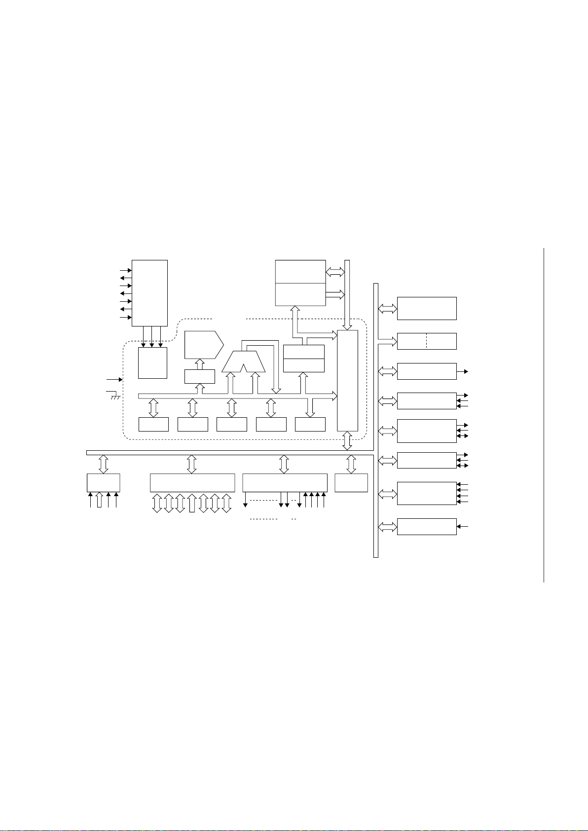
BLOCK DIAGRAM
V
DD
GND
RAM
(384 bytes)
TBC
WDT
BUZZER OUTPUT
8-bit TIMER ¥ 3
8-bit SHIFT REG.
(16-BYTE AUTOMATIC
TRANSFER FUNCTION)
BZ*
T1OUT*
T0CK*
GATE*
SFTO0*
SFTI0*
SFTCK0*
8-bit SHIFT REG.
SFTO1*
SFTI1*
SFTCK1*
INTERRUPT
CONT.
INT0*
INT1*
INT2*
INT3*
REMOTE CONT.
RMCIN*
BUS
CONT.
RAM
(256 bytes)
ROM
(24K bytes)
LCD DRIVER
V
DD3VDD2VDD1VDDL
COM1
COM4
SEG0
SEG31
I/O PORT
8-bit A/D C
¥ 8ch
AVDDV
RH
AGND
AI0-7*
GMAR
PC
LMARSPPSWBRAR
ALU
IR
T/C
INST.
DEC.
OSC.
CONT.
XT
XT
OCS0
OSC1
RESET
CLKOUT*
XSTOP*
*secondary function of each port
**The MSM65353A contains 16K byte ROM only
CPU CORE
WATCH
TIMER
P6
P5
P4
P3
P2
P1
P0

¡ Semiconductor MSM65354/65353A
,
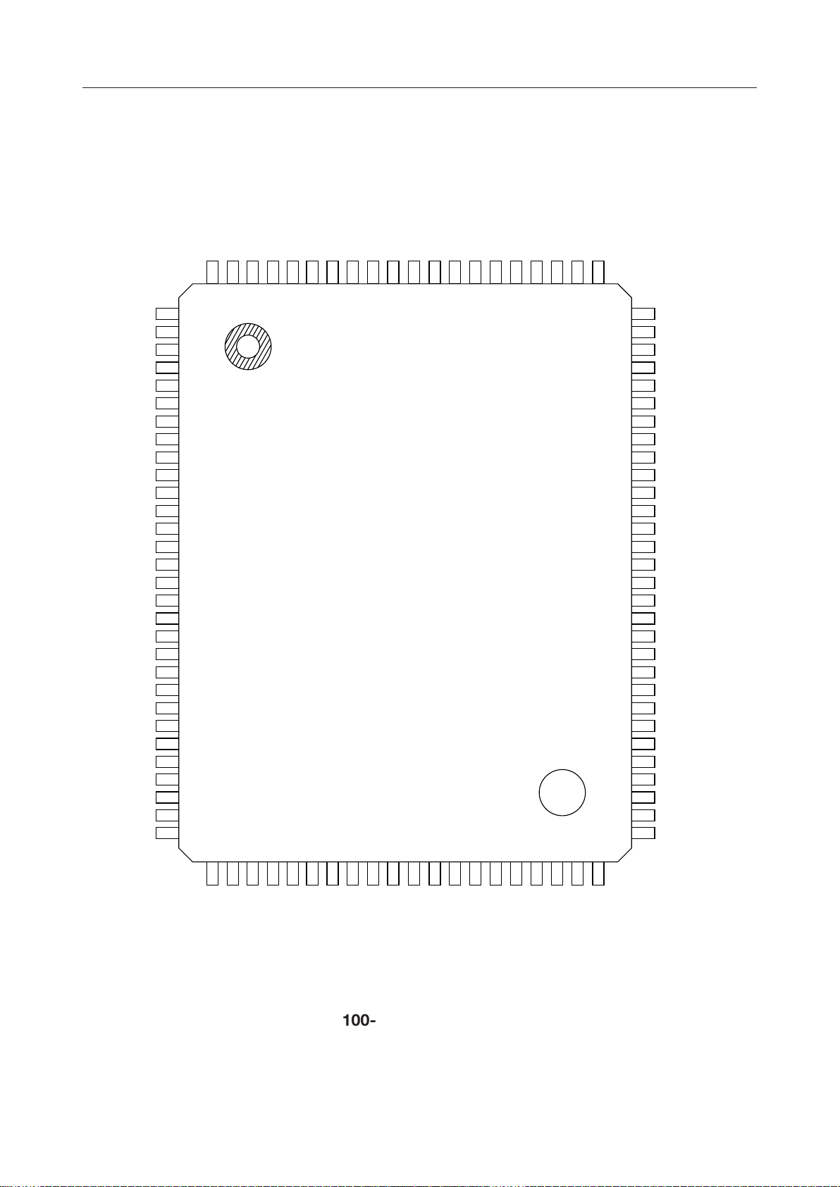
PIN CONFIGURATION (TOP VIEW)
DDL
DD1
DD2
COM1
COM2
COM3
COM4
SEG0
SEG1
SEG2
SEG3
SEG4
SEG5
SEG6
SEG7
SEG8
SEG9
SEG10
SEG11
SEG12
SEG13
SEG14
SEG15
SEG16
SEG17
SEG18
SEG19
SEG20
SEG21
SEG22
SEG23
SEG24
SEG25
10
11
12
13
14
15
16
17
18
19
20
21
22
23
24
25
26
27
28
29
30
DD3
V
V
V
98
99
100
1
2
3
4
5
6
7
8
9
P6.1 (OUT)
V
96
97
P6.0 (IN)
P2.0/SFTCK0
RESET
93
94
95
P2.3/INT2
P2.2/SFTO0
P2.1/SFTI0
90
91
92
P2.4
89
P2.5
88
P2.6
87
P2.7
86
XT
85
XT
84
GND
83
OSC0
82
OSC1
81
P0.0/INT0
80
79
P0.1/HSTOP
78
P0.2/T1OUT
77
P0.3/T1OUT
76
P0.4/INT1/GATE
75
P0.5/CLKOUT
P0.6
74
73
P0.7/BZ
72
V
DD
P1.0
71
70
P1.1
69
P1.2
68
P1.3
67
P1.4/RMCIN
66
P1.5/SFTCK1
65
P1.6/SFTI1
64
P1.7/SFTO1
63
P4.0
62
P4.1
61
P4.2
60
P4.3
59
P4.4
58
P4.5
57
P4.6
56
P4.7
55
P5.0
54
P5.1
53
P5.2
52
P5.3
51
P5.4
50
49
48
47
46
45
44
43
42
41
40
39
38
37
36
35
34
33
32
31
DD
RH
SEG27
SEG26
SEG29
SEG28
SEG31
SEG30
AGND
P3.1/AI1/INT3
P3.0/AI0/INT3
P3.5/AI5
P3.4/AI4
P3.3/AI3/INT3
P3.2/AI2/INT3
P3.7/AI7
P3.6/AI6
V
AV
P5.7
P5.6
P5.5
100-Pin Plastic QFP
4/20

¡ Semiconductor MSM65354/65353A
PIN DESCRIPTIONS
Basic Function
Function Pin Type Description
72 — Digital supply voltage (5V)
83 — Digital ground
47 — Analog supply voltage (5V)
Power Supply
37 — Analog ground
98 — Bias supply pin for LCD driver
99 — Bias supply pin for LCD driver
100 — Bias supply pin for LCD driver
97 — Bias control pin for LCD driver
Symbol
V
DD
GND
AV
DD
AGND
V
DD1
V
DD2
V
DD3
V
DDL
Oscillation input pin on the OSC side:
82 I
OSC0
Connect to a quartz oscillator (ceramic resonator),
or input external clock.
Oscillation output pin on the OSC side:
Oscillation
81 O
OSC1
Connect to a quartz oscillator (ceramic resonator).
When external clock is input to the OSC0 pin, the
OSC1 pin should be open.
84 I
XT
Oscillation input pin on the XT side:
Connect to a quartz oscillator of 32.768kHz.
85 O
XT
Oscillation output pin on the XT side:
Connect to a quartz oscillator of 32.768kHz.
5/20

¡ Semiconductor MSM65354/65353A
Basic Function (Continued)
Function Pin Type Description
Control
Ports
94
80
to
73
71
to
64
Symbol
RESET
P0.0
to
P0.7
P1.0
to
P1.7
I/O
I/O
System reset input:
When this pin is set to the "L" level, the internal
I
status is initialized to start execution of
instructions from address 0040H. The input is
pulled up to V
8-bit input-output port (port 0):
Each of bits 0 to 7 is configured to be input or
output by use of the direction register of port 0
(P0DIR). In addition to the basic function as the
input-output port, a secondary function is allocated
to each of P0.0 through P0.7. See Secondary function.
8-bit input-output port (port 1):
Each of bits 0 to 7 is configured to be input or
output by use of the direction register of port 1
(P1DIR). In addition to the basic function as the
input-output port, a secondary function is allocated
to each of P1.0 through P1.7. See Secondary function.
with an internal pull-up resistor.
DD
93
86
to
P2.0
to
P2.7
I/O
8-bit input-output port (port 2):
Each of bits 0 to 7 is configured to be input or
output by use of the direction register of port 2
(P2DIR). In addition to the basic function as the
input-output port, a secondary function is allocated
to each of P2.0 through P2.3. See Secondary function.
6/20
