OKI MSM65352B-xxxGS-BK, MSM65352-xxxGS-BK Datasheet

E2E1019-27-Y3
¡ Semiconductor MSM65352/65352B
¡ Semiconductor
This version: Jan. 1998
Previous version: Nov. 1996
MSM65352/65352B
8-Bit Microcontroller with 4-Bit A/D Converter (with LCD Driver)
GENERAL DESCRIPTION
The MSM65352 is a high performance 8-bit microcontroller that employs OKI original CPU core,
the nX-8/50. The MSM65352 includes 8K-byte program memory, 256-byte data memory, LCD
driver, timer, serial I/O and 4-bit A/D converter. Also available is the MSM65352B, which has four
LCD outputs in place of four output ports. Also available are the MSM65P352 and MSM65P352B,
which replace the on-chip program memory with one-time PROM.
FEATURES
• Operating range
Operating voltage : 2.7V to 5.5V
Operating temperature : –20°C to +70°C
Operating frequency: High speed side : 0 to 10MHz (@V
(dual clock) : 0 to 5MHz (@VDD=2.7V to 5.5V)
Low speed side : 32.768kHz (@VDD=2.7V to 5.5V)
• Current consumption (Typ.): High speed side : 5mA (@5MHz, VDD=3V)
20mA (@10MHz, VDD=5V)
1.5mA (@5MHz, VDD=3V, halt mode)
Low speed side : 45mA (@32.768kHz, VDD=3V)
4mA (@VDD=3V, stop mode)
• Minimum instruction execution time : 400ns (@10MHz), 800ns (@5MHz)
• CPU core : 8-bit CPU core nX-8/50
• General memory space : 8K-byte program memory
• Local memory space : 256-byte data memory + SFR
• LCD driver : 16 ¥ 4 (MSM65352), 20 ¥ 4 (MSM65352B)
• I/O port : 5 ports, 31 bits (MSM65352)
4 ports, 27 bits (MSM65352B)
Input-output port : 2 ports ¥ 8 bits, 1 port ¥ 1 bit
Input port : 1 port ¥ 1 bit
1 port ¥ 4 bits (Only for MSM65352)
Output port : 1 port ¥ 8 bits, 1 port ¥ 1 bit
• Timer : 8-bit auto-reload timer ¥ 2
Watchdog timer ¥ 1
Watch timer
(counter clock is fixed at XT=32.768kHz)
• Counter : Time base counter ¥ 1 (14 bits)
• Serial I/O : 1ch, clock sync ¥ 1
• A/D converter : 4-bit ¥ 8-ch, with reference current cutoff function
• Remote control input circuit :
• Interrupt source : 9 sources
• Package:
64-pin plastic QFP (QFP64-P-1414-0.80-BK)(Product name: MSM65352-¥¥¥GS-BK,
Receives signal in 32kHz/5MHz/10MHz operations
MSM65352B-¥¥¥GS-BK)
¥¥¥ indicates the code number.
=5V±10%)
DD
1/15

¡ Semiconductor MSM65352/65352B
• Others : CPU clock can be an OSC, half-OSC, or XT clock.
Time base counter can be selected with 1/4n of a
CPU clock (n=1 to 8).
2/15

3/15
¡ Semiconductor MSM65352/65352B
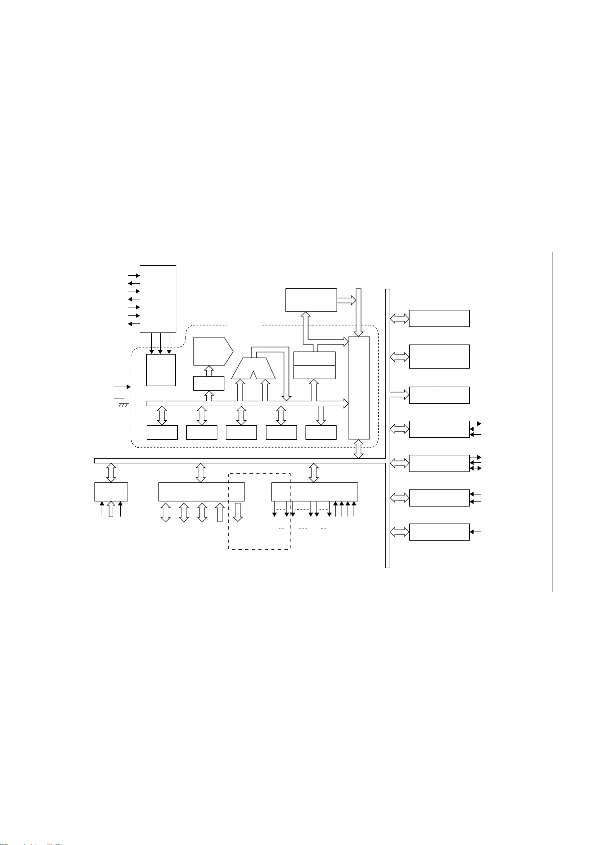
BLOCK DIAGRAM
V
DD
GND
RAM
(256 bytes)
TBC
WDT
8-bit TIMER ¥ 2
T1OUT*
T0CK*
GATE*
SFTO1*
SFTI1*
SFTCK1*
INTERRUPT CONT.
INT0*
INT1*
REMOTE CONT.
RMCIN*
BUS
CONT.
ROM
(8K bytes)
I/O PORT
P4**
4-bit A/D C
¥ 8ch
AGND
AVDDAI0-7*
GMAR
PC
LMARSPPSWBRAR
ALU
IR
T/C
INST.
DEC.
OSC.
CONT.
XT
XT
OCS0
OSC1
RESET
HSTOP*
CLKOUT*
*Secondary function of each port.
**P4: for the MSM65352
SEG16-19: for the MSM65352B
SIO (SYNC MODE)
WATCH TIMER
LCD DRIVER
V
DDLVDD3VDD2VDD1
COM1
COM4
SEG0
SEG19**
SEG15
SEG16**
CPU CORE
P3
P2
P1
P0

¡ Semiconductor MSM65352/65352B
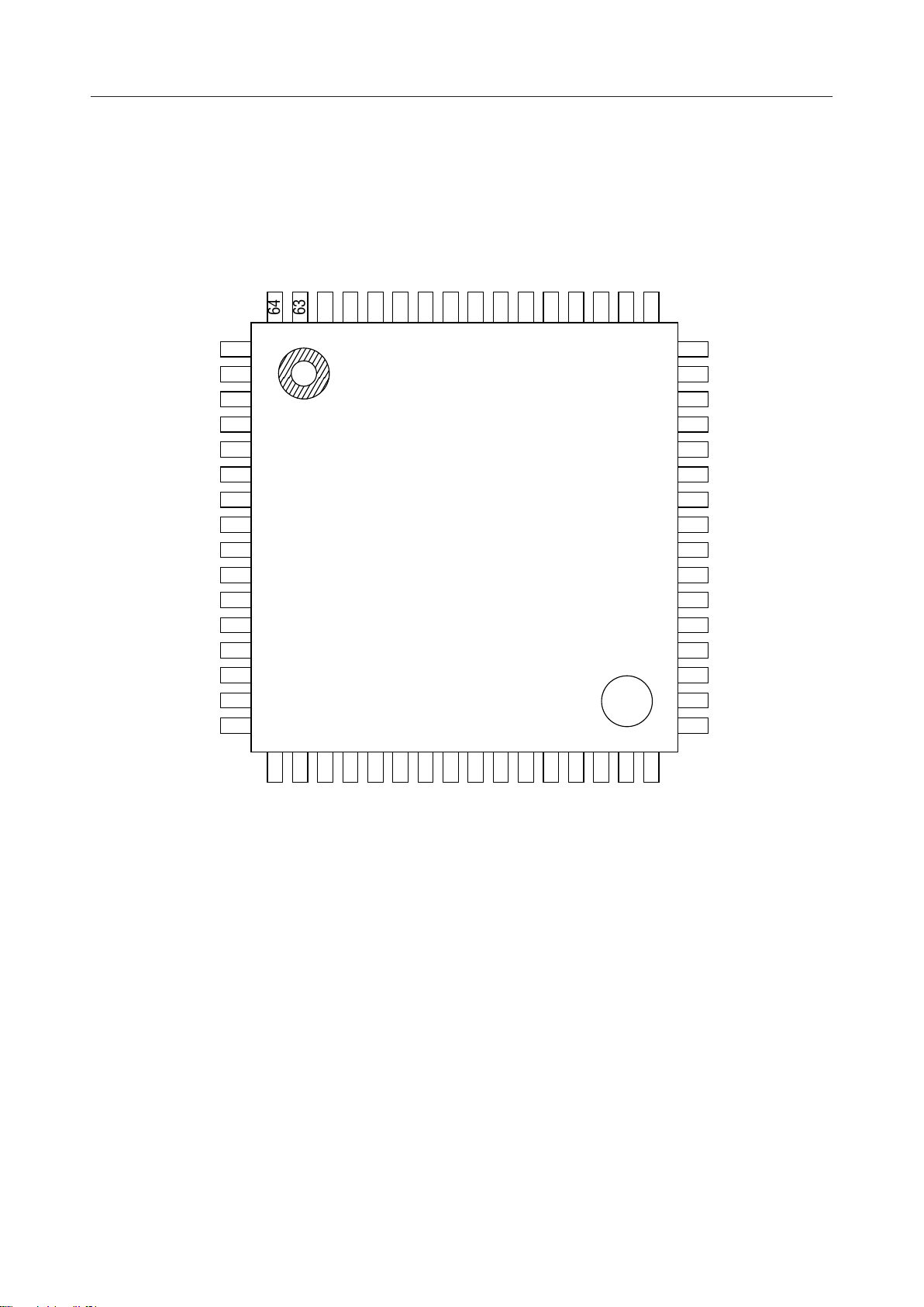
PIN CONFIGURATION (TOP VIEW)
DD
P1.0
P1.1
P1.2
P1.3
P1.4/RMCIN
P1.5/SFTCK1
P1.6/SFTI1
P1.7/SFTO1
P2.0(IN)
55
P2.1(TEST)
54
53 P2.2
52 P4.3****
54 P4.2***
50 P4.1**
49 P4.0*
V
64
63
62
61
60
59
58
57
56
P0.7
P0.6
P0.5/CLKOUT
P0.4/INT1/GATE
P0.3/T0CK
P0.2/T1OUT
P0.1/HSTOP
P0.0/INT0
OSC0
OSC1
GND
1
2
3
4
5
6
7
8
9
10
11
12XT
13XT
14RESET
15AGND
16P3.7/AI7
17
18
P3.6/AI6
P3.5/AI5
19
20
P3.4/AI4
P3.3/AI3
21
22
P3.2/AI2
P3.1/AI1
23
24
DD
AV
P3.0/AI0
25
26
27
DD3VDD2VDD1
V
48
SEG15
47
SEG14
46
SEG13
45
SEG12
44
SEG11
43
SEG10
42
SEG9
41
SEG8
40
SEG7
39
SEG6
38
SEG5
37 SEG4
36 SEG3
35 SEG2
34 SEG1
33 SEG0
28V
29COM1
30COM2
31COM3
32COM4
DDL
* SEG16 for MSM65352B
** SEG17 for MSM65352B
*** SEG18 for MSM65352B
**** SEG19 for MSM65352B
64-Pin Plastic QFP
4/15

¡ Semiconductor MSM65352/65352B
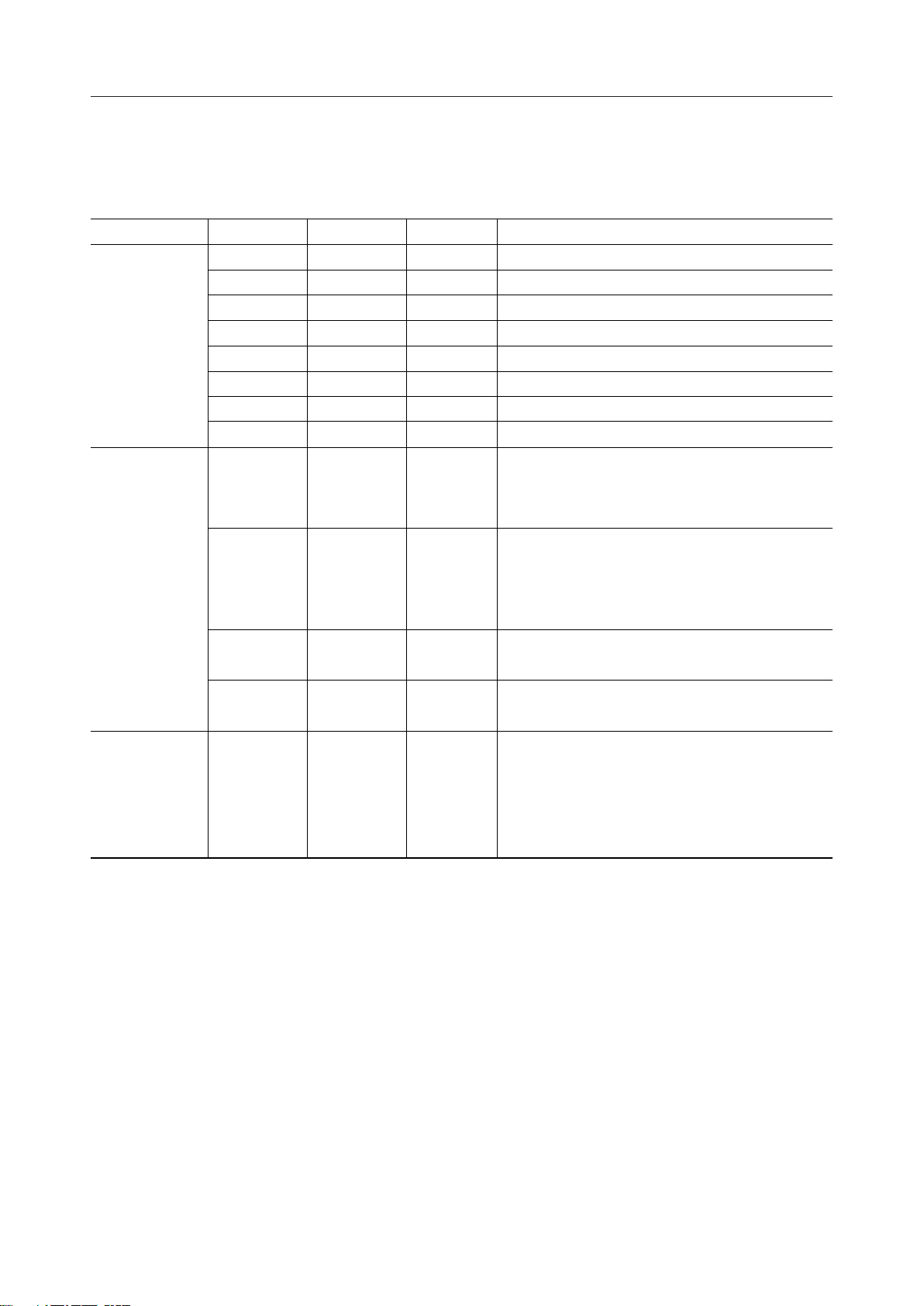
PIN DESCRIPTION
Basic Function
Function Pin Type Description
64 — Digital supply voltage (5V)
11 — Digital ground
24 — Analog supply voltage (5V)
Power Supply
15 — Analog ground
27 — Bias input for LCD driver
26 — Bias input for LCD driver
25 — Bias input for LCD driver
28 — Ground for LCD driver bias
Symbol
V
DD
GND
AV
DD
AGND
V
DD1
V
DD2
V
DD3
V
DDL
Oscillation input pin on the OSC side:
9I
OSC0
Connect to a quartz oscillator (ceramic resonator),
or input external clock.
Oscillation output pin on the OSC side:
Oscillation
10 O
OSC1
Connect to a quartz oscillator (ceramic resonator).
When external clock is input to the OSC0 pin, the
OSC1 pin should be kept open.
13 I
XT
Oscillation input pin on the XT side:
Connect to a quartz oscillator of 32.768kHz.
12 O
XT
Oscillation output pin on the XT side:
Connect to a quartz oscillator of 32.768kHz.
System reset input:
When this pin is set to the "L" level, the internal
Control 14 I
RESET
status is initialized to start execution of
instructions from address 0040H. The input is
pulled up to V
with an internal pull-up resistor.
DD
5/15
 Loading...