

NSC 5962-9953501QXA Datasheet
54LCX16374
Low Voltage 16-Bit D Flip-Flop with 5V Tolerant Inputs
and Outputs
General Description
The LCX16374 contains sixteen non-inverting D flip-flops
with TRI-STATE
®
outputs and is intended for bus oriented
applications. The device is byte controlled. A buffered clock
(CP) and OutputEnable (OE) are common to each byte and
can be shorted together for full 16-bit operation.
The LCX16374 is designed for low voltage (3.3V) V
CC
applications with capability of interfacing to a 5V signal environment.
The LCX16374 is fabricated with an advanced CMOS technology to achieve high speed operation while maintaining
CMOS low power dissipation.
Features
n 5V tolerant inputs and outputs
n Power down high impedance inputs and outputs
n Supports live insertion/withdrawal
n 2.0V–3.6V V
CC
supply operation
n
±
24 mA output drive
n Implements patented noise/EMI reduction circuitry
n Functionally compatible with the 54 series 16374
n ESD performance:
Human body model
>
2000V
Machine model
>
200V
n Standard Microcircuit Drawing (SMD) 5962-99535
Ordering Code
Order Number Package Number Package Description
54LCX16374W-QML WA48A 48-Lead Ceramic Flatpack
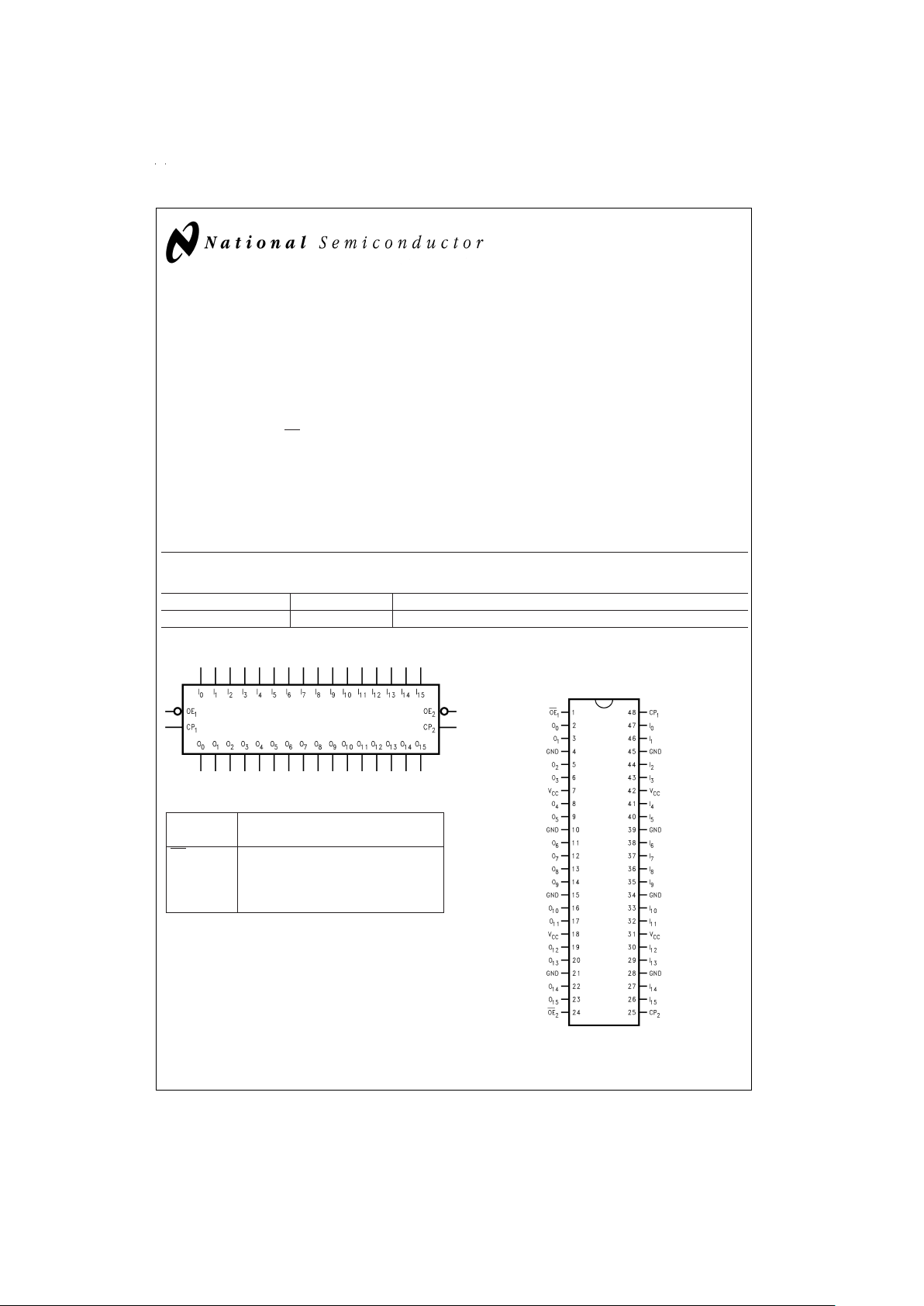
Logic Symbol
Pin Descriptions
Pin Description
Names
OE
n
Output Enable Input (Active Low)
CP
n
Clock Pulse Input
I
0–I15
Inputs
O
0–O15
Outputs
Connection Diagram
TRI-STATE®is a registered trademark of National Semiconductor Corporation.
DS101199-1
Pin Assignment for
Cerpack
DS101199-2
July 1999
54LCX16374 Low Voltage 16-Bit D Flip-Flop with 5V Tolerant Inputs and Outputs
© 1999 National Semiconductor Corporation DS101199 www.national.com

Functional Description
The LCX16374 consists of sixteen edge-triggered flip-flops
with individual D-type inputs andTRI-STATE true outputs.
The device is byte controlled with each byte functioning identically, but independent of the other. The control pins can be
shorted together to obtain full 16-bit operation. Each byte
has a buffered clock and buffered Output Enable common to
all flip-flops within that byte. The description which follows
applies to each byte. Each flip-flop will store the state of their
individual D inputs that meet the setup and hold time requirements on the LOW-to-HIGH Clock (CP
n
) transition. With the
Output Enable (OE
n
) LOW, the contents of the flip-flops are
available at the outputs. When OEnis HIGH, the outputs go
to the high impedance state. Operation of the OEninput
does not affect the state of the flip-flops.
Inputs Outputs
CP
1
OE
1
I0–I
7
O0–O
7
LH H
LL L
LL X O
0
XH X Z
Inputs Outputs
CP
2
OE
2
I8–I
15
O8–O
15
LH H
LL L
LL X O
0
XH X Z
H
=
High Voltage Level
L=Low Voltage Level
X=Immaterial
Z=High Impedance
O
0
=
Previous O
0
before HIGH to LOW of CP
Logic Diagrams
Byte 1 (0:7)
DS101199-3
Byte 2 (8:15)
DS101199-4
Please note that this diagram is provided only for the understanding of logic operations and should not be used to estimate propagation delays.
www.national.com 2
 Loading...