NSC 5962-9950501QXA Datasheet

54LCX16244
Low Voltage 16-Bit Buffer/Line Driver with 5V Tolerant
Inputs and Outputs
General Description
The LCX16244 contains sixteen non-inverting buffers with
TRI-STATE
®
outputs designedto be employed as a memory
and address driver, clock driver, or bus oriented transmitter/
receiver. The device is nibble controlled. Each nibble has
separate TRI-STATE control inputs which can be shorted together for full 16-bit operation.
The LCX16244 is designed for low voltage (3.3V) V
CC
applications with capability of interfacing to a 5V signal environment.
The LCX16244 is fabricated with an advanced CMOS technology to achieve high speed operation while maintaining
CMOS low power dissipation.
Features
n 5V tolerant inputs and outputs
n Power down high impedance inputs and outputs
n Supports live insertion/withdrawal
n 2.0V–3.6V V
CC
supply operation
n
±
24 mA output drive
n Implements patented noise/EMI reduction circuitry
n Functionally compatible with 54 series 16244
n ESD performance:
Human body model
>
2000V
Machine model
>
200V
n Standard Microcircuit Drawing (SMD) 5962-9950501
Ordering Code
Order Number Package Number Package Description
54LCX16244W-QML WA48A 48-Lead Cerpack Package
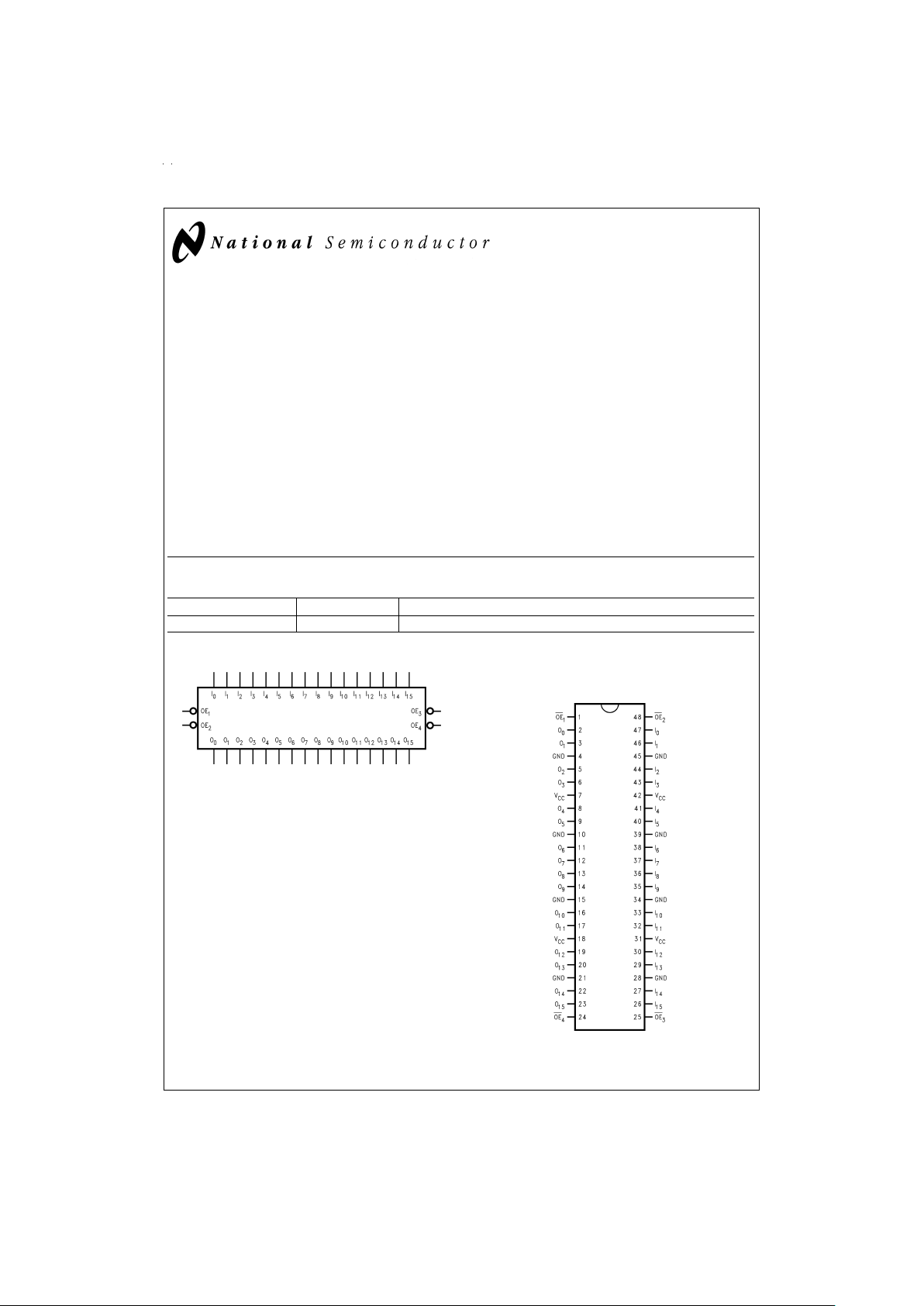
Logic Symbol Connection Diagram
TRI-STATE®is a registered trademarkof National Semiconductor Corporation.
DS101059-1
Pin Assignment for
Cerpack
DS101059-2
April 1999
54LCX16244 Low Voltage 16-Bit Buffer/Line Driver with 5V Tolerant Inputs and Outputs
© 1999 National Semiconductor Corporation DS101059 www.national.com

Pin Descriptions
Pin Names Description
OE
n
Output Enable Input (Active Low)
I
0–I15
Inputs
O
0–O15
Outputs
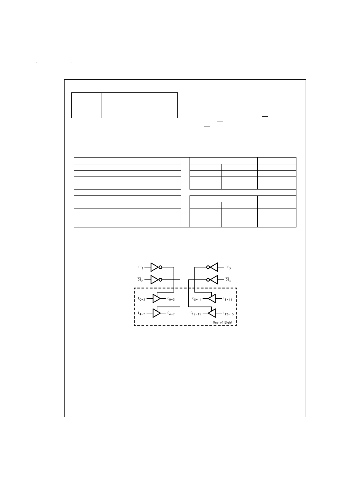
Functional Description
The LCX16244 contains sixteen non-inverting buffers with
TRI-STATE standard outputs. The device is nibble (4 bits)
controlled with each nibble functioning identically, but independent of the other. The control pins can be shorted together to obtainfull 16-bit operation.The TRI-STATEoutputs
are controlled by an Output Enable (OE
n
) input for each
nibble. When OEnis LOW, the outputs are in bi-state mode.
When OEnis HIGH, the outputs are in the high impedance
mode, butthis does not interfere with entering new data into
the inputs.
Truth Tables
Inputs Outputs Inputs Outputs
OE
1
I0–I
3
O0–O
3
OE
2
I4–I
7
O4–O
7
LL L LL L
LH H LH H
HX Z HX Z
Inputs Outputs Inputs Outputs
OE
3
I8–I
11
O8–O
11
OE
4
I12–I
15
O12–O
15
LL L LL L
LH H LH H
HX Z HX Z
H
=
High Voltage Level
L=Low Voltage Level
X=Immaterial
Z=High Impedance
Logic Diagram
DS101059-3
www.national.com 2
 Loading...