NSC 5962-9860601QLA, 5962-9860601QKA Datasheet

54LVX4245
8-Bit Dual Supply Translating Transceiver with
TRI-STATE
®
Outputs
General Description
The LVX4245 is a dual-supply, 8-bit translating transceiver
that is designed to interface between a 5V bus and a 3V bus
in a mixed 3V/5Vsupplyenvironment.The Transmit/Receive
(T/R) input determines the direction of data flow. Transmit
(active-HIGH) enables data from A ports to B ports; Receive
(active-LOW) enables data from B ports to A ports. The Output Enable input, when HIGH, disables bothA and B ports by
placing them in a TRI-STATE condition. TheA port interfaces
with the 5V bus; the B port interfaces with the 3V bus.
The LVX4245is suitable for mixed voltage applications such
as systems using 3.3V memories which must interface with
existing buses or other components operating at 5.0V.
Features
n Bidirectional interface between 5V and 3V buses
n Control inputs compatible with TTL level
n 5V data flow at A port and 3V data flow at B port
n Outputs source/sink 24 mA
n Available in Ceramic DIP and Flatpack packages
n Implements patented EMI reduction circuitry
n Functionally compatible with the 54 series 245
n Standard Microcircuit Drawing (SMD) 5962-9860601
Ordering Code
Order Number Package Number Package Description
54LVX4245J-QML J24F 24-Lead Ceramic Dual-in-line
54LVX4245W-QML W24C 24-Lead Cerpack
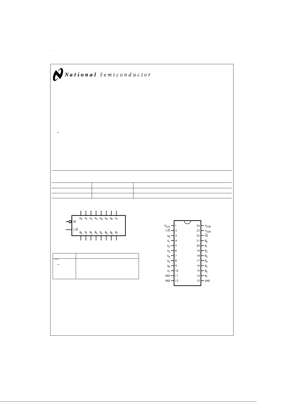
Logic Symbol
Pin Descriptions
Pin Names Description
OE
Output Enable Input
T/R
Transmit/Receive Input
A
0–A7
Side A Inputs or TRI-STATE Outputs
B
0–B7
Side B Inputs or TRI-STATE Outputs
Connection Diagram
TRI-STATE®is a registered trademark of National Semiconductor
DS101021-1
Pin Assignment for
CDIP and Cerpack
DS101021-2
January 1999
54LVX4245 8-Bit Dual Supply Translating Transceiver with TRI-STATE Outputs
© 1999 National Semiconductor Corporation DS101021 www.national.com

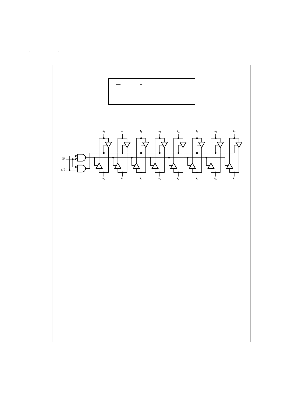
Truth Table
Inputs Outputs
OE
T/R
L L Bus B Data to Bus A
L H Bus A Data to Bus B
H X HIGH-Z State
H=High Voltage Level
L=Low Voltage Level
X=Immaterial
Logic Diagram
DS101021-6
www.national.com 2

Absolute Maximum Ratings (Note 1)
If Military/Aerospace specified devices are required,
please contact the National Semiconductor Sales Office/
Distributors for availability and specifications.
Supply Voltage (V
CCA,VCCB
) −0.5V to +7.0V
DC Input Voltage (V
I
)@OE , T/R −0.5V to V
CCA
+ 0.5V
DC Input/Output Voltage (V
I/O
)
@
A(n) −0.5V to V
CCA
+ 0.5V
@
B(n) −0.5V to V
CCB
+ 0.5V
DC Input Diode Current (I
IN
)
@
OE , T/R
±
20 mA
DC Output Diode Current (I
OK
)
±
50 mA
DC Output Source or Sink Current
(I
O
)
±
50 mA
DC V
CC
or Ground Current
per Output Pin (I
CC
or I
GND
)
±
50 mA
and Max Current
@
I
CCA
±
200 mA
@
I
CCB
±
200 mA
Storage Temperature Range
(T
STG
) −65˚C to +150˚C
Recommended Operating
Conditions
(Note 2)
Supply Voltage
V
CCA
4.5V to 5.5V
V
CCB
2.7V to 3.6V
Input Voltage (V
I
)@OE , T/R 0V to V
CCA
Input/Output Voltage (V
I/O
)
@
A(n) 0V to V
CCA
@
B(n) 0V to V
CCB
Free Air Operating Temperature (TA)
54LVX −55˚C to +125˚C
Minimum Input Edge Rate (∆t/∆V) 8 ns/V
V
IN
from 30%to 70%of V
CC
V
CC
@
3.0V, 4.5V, 5.5V
Note 1: The “Absolute Maximum Ratings” are those values beyond which
the safety of the device cannot be guaranteed. The device should not be operated at these limits. The parametric values defined in the Electrical Characteristics tables are not guaranteed at the absolute maximum ratings. The
“Recommended Operating Conditions” table will define the conditions for actual device operation.
Note 2: Unused inputs must he held HIGH or LOW. They may not float.
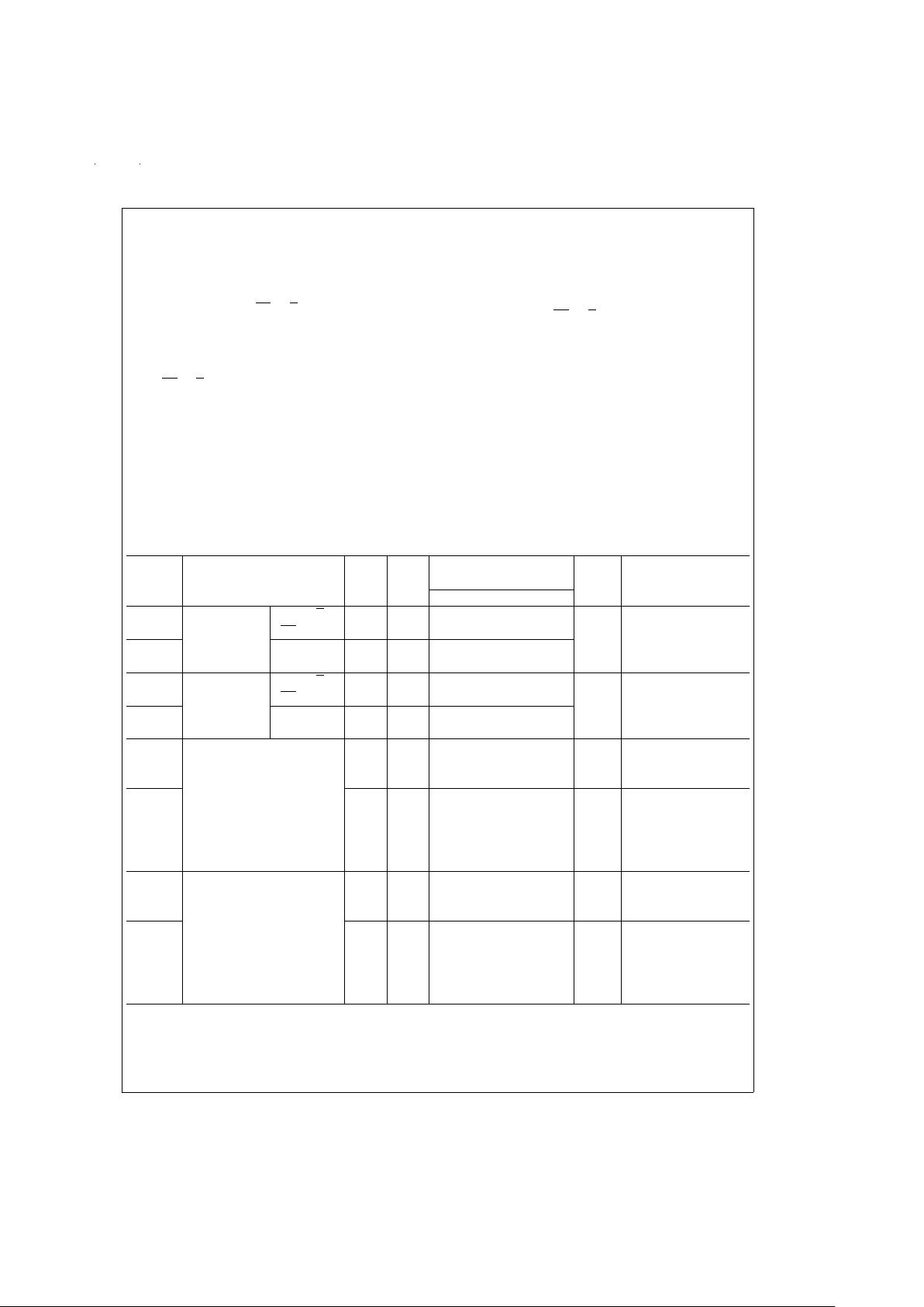
DC Electrical Characteristics
Symbol Parameter V
CCA
(V)
V
CCB
(V)
T
A
=
−55˚C to +125˚C Units Conditions
Guaranteed Limits
V
IHA
Minimum A(n), T/R , 5.5 3.3 2.0 V V
OUT
≤ 0.1V or
High Level OE
4.5 3.3 2.0 ≥ VCC− 0.1V
V
IHB
Input Voltage B(n) 5.0 3.6 2.0
5.0 2.7 2.0
V
ILA
Maximum A(n), T/R , 5.5 3.3 0.8 V V
OUT
≤ 0.1V or
Low Level OE
4.5 3.3 0.8 ≥ VCC−0.1V
V
ILB
Input Voltage B(n) 5.0 2.7 0.8
5.0 3.6 0.8
V
OHA
Minimum High Level 4.5 2.7 4.4 V I
OH
=
−100 µA
Output Voltage 5.5 3.6 5.4 I
OH
=
−100 µA
4.5 3.0 3.7 I
OH
=
−24 mA
V
OHB
4.5 2.7 2.6 V I
OH
=
−100 µA
5.5 3.6 3.5 I
OH
=
−100 µA
4.5 2.7 2.2 I
OH
=
−12 mA
4.5 3.0 2.4 I
OH
=
−12 mA
4.5 3.0 2.2 I
OH
=
−24 mA
V
OLA
Maximum Low Level 4.5 2.7 0.1 V I
OL
=
100 µA
Output Voltage 5.5 3.6 0.1 I
OL
=
100 µA
4.5 3.0 0.4 I
OL
=
24 mA
V
OLB
4.5 2.7 0.1 I
OL
=
100 µA
5.5 3.6 0.1 V I
OL
=
100 µA
4.5 2.7 0.4 I
OL
=
12 mA
4.5 3.0 0.3 I
OL
=
12 mA
4.5 3.0 0.4 I
OL
=
24 mA
www.national.com3
 Loading...