

NSC 5962-9754302QSA, 5962-9754302QRA, 5962-9754302Q2A Datasheet

54LCX245
Low Voltage Bidirectional Transceiver with 5V Tolerant
Inputs and Outputs
General Description
The LCX245 contains eight non-inverting bidirectional buffers with TRI-STATE
™
outputs and is intended for bus oriented applications. The device is designed for low voltage
(3.3V) V
CC
applications with capability of interfacing to a 5V
signal environment. The T/R input determines the direction
of data flow through the device. The OE input disables both
theAandBports by placing them in a high impedance state.
The LCX245 is fabricated with an advanced CMOS technology to achieve high speed operation while maintaining
CMOS low power dissipation.
Features
n 5V tolerant inputs and outputs
n 9ns t
PD
max, 10µA I
CCQ
max
n Power down high impedance inputs and outputs
n Supports live insertion/withdrawal
n 2.0V–3.6V V
CC
supply operation
n
±
24 mA output drive
n Implements patented noise/EMI reduction circuitry
n Functionally compatible with the 54 series 245
n ESD performance:
Human body model
>
2000V
Machine model
>
200V
n Standard Microcircuit Drawing (SMD) 5962-97543
Logic Symbols
Pin Descriptions
Pin Names Description
OE
Output Enable Input
T/R
Transmit/Receive Input
A
0–A7
Side A Inputs or 3-STATE Outputs
B
0–B7
Side B Inputs or 3-STATE Outputs
Connection Diagram
TRI-STATE®is a registered trademark of National Semiconductor Corporation.
DS101022-1
Pin Assignment
for DIP and Cerpack
DS101022-3
Pin Assignment
for LCC
DS101022-6
December 1998
54LCX245 Low Voltage Bidirectional Transceiver with 5V Tolerant Inputs and Outputs
© 1998 National Semiconductor Corporation DS101022 www.national.com
Truth Table
Inputs Outputs
OE
T/R
L L Bus B0–B7Data to Bus A0–A
7
L H Bus A0–A7Data to Bus B0–B
7
H X HIGH Z State on A0–A7,B0–B7(Note 1)
H=High Voltage Level
L=Low Voltage Level
X=Immaterial
Z=High Impedance
Note 1: Unused bus terminals during HIGH Z State must be held HIGH or LOW.
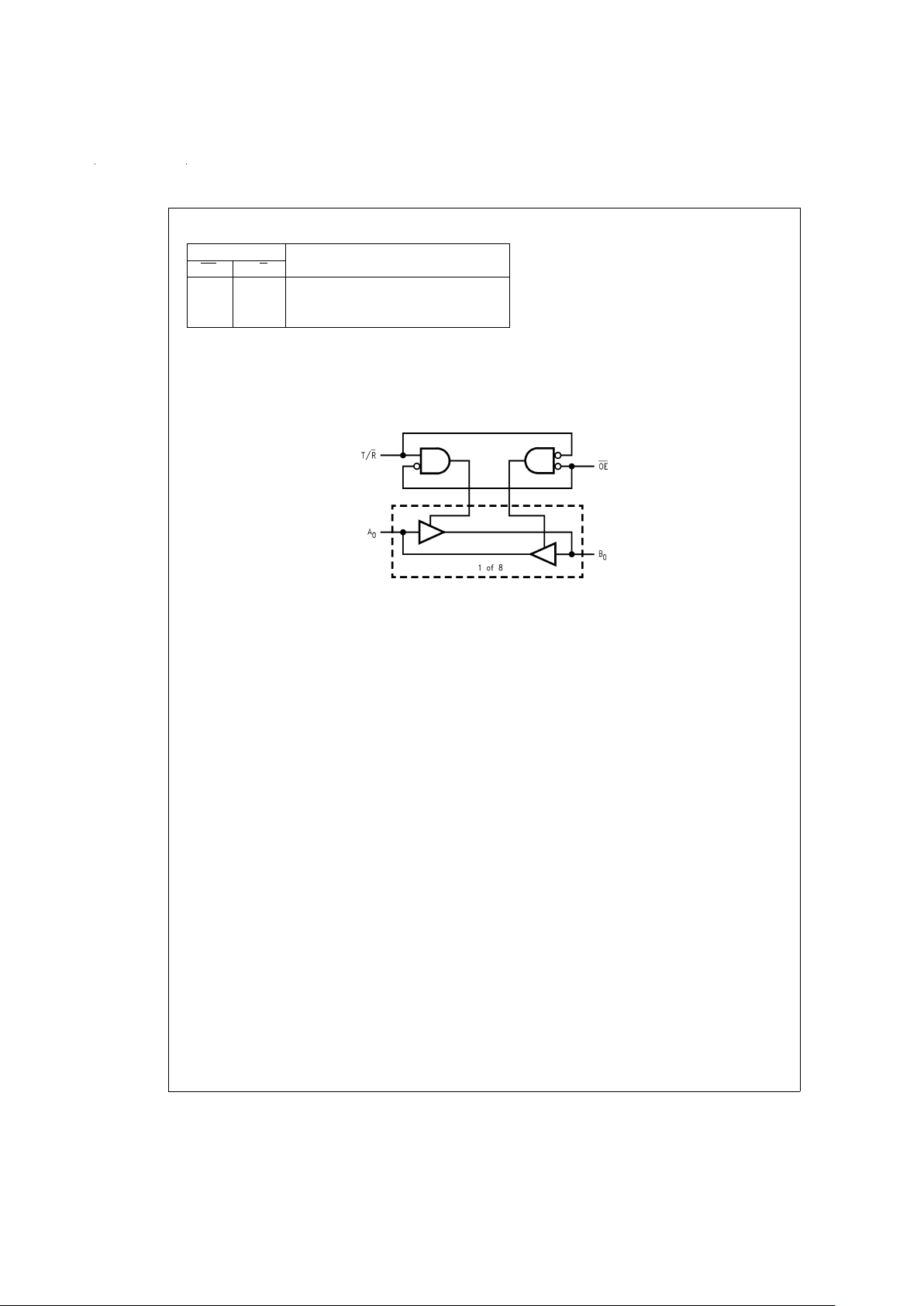
Logic Diagram
DS101022-4
www.national.com 2
 Loading...