NSC 5962-9687001QXA Datasheet

54ABT16500
18-Bit Universal Bus Transceivers with TRI-STATE
®
Outputs
General Description
These 18-bit universal bus transceivers combine D-type
latches and D-type flip-flops to allow data flow in transparent,
latched, and clocked modes.
Data flow in each direction is controlled by output-enable
(OEAB and OEBA), latch-enable (LEAB and LEBA), and
clock (CLKAB and CLKBA) inputs. For A-to-B data flow, the
device operates in the transparent mode when LEAB is high.
When LEAB is low, the A data is latched if CLKAB is held at
a high or low logic level. If LEAB is low, the A bus data is
stored in the latch/flip-flop on the high-to-low transition of
CLKAB. Output-enable OEAB is active-high. When OEAB is
high, the outputs are active. When OEAB is low, the outputs
are in the high-impedance state.
Data flow for B to AissimilartothatofAto B but uses OEBA,
LEBA, and CLKBA. The output enables are complementary
(OEAB is active high and OEBA is active low).
To ensure the high-impedance state during power up or
power down, OE should be tied to GND through a pulldown
resistor; the minimum value of the resistor is determined by
the current-sourcing capability of the driver.
Features
n Combines D-Type latches and D-Type flip-flops for
operation in transparent, latched, or clocked mode
n Flow-through architecture optimizes PCB layout
n Guaranteed latch-up protection
n High impedance glitch free bus loading during entire
power up and power down cycle
n Non-destructive hot insertion capability
n Standard Microcircuit Drawing (SMD) 5962-9687001
Ordering Code
Military Package Package Description
Number
54ABT16500W-QML WA56A 56-Lead Cerpack
TRI-STATE®is a registered trademark of National Semiconductor Corporation.
July 1998
54ABT16500 18-Bit Universal Bus Transceivers with TRI-STATE Outputs
54ABT16500
© 1998 National Semiconductor Corporation DS100225 www.national.com
1
PrintDate=1998/07/14 PrintTime=11:08:55 43605 ds100225 Rev. No. 1 cmserv
Proof 1

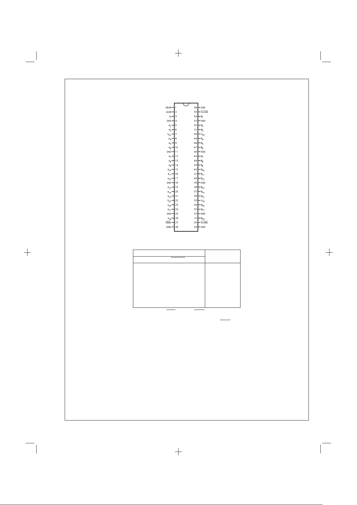
Connection Diagram
Function Table
(Note 1)
Inputs Output
B
OEAB LEAB CLKAB
A
LX X X Z
HH X L L
HH X H H
HL
↓
LL
HL
↓
HH
HL HXB
0
(Note 2)
HL L XB
0
(Note 3)
Note 1: A-to-B data flow is shown: B-to-A flow is similar but uses OEBA, LEBA, and CLKBA.
Note 2: Output level before the indicated steady-state input conditions were established.
Note 3: Output level before the indicated steady-state input conditions were established, provided that CLKAB was low before LEAB went low.
Pin Assignment for Cerpack
DS100225-1
PrintDate=1998/07/14 PrintTime=11:08:55 43605 ds100225 Rev. No. 1 cmserv Proof 2
www.national.com 2

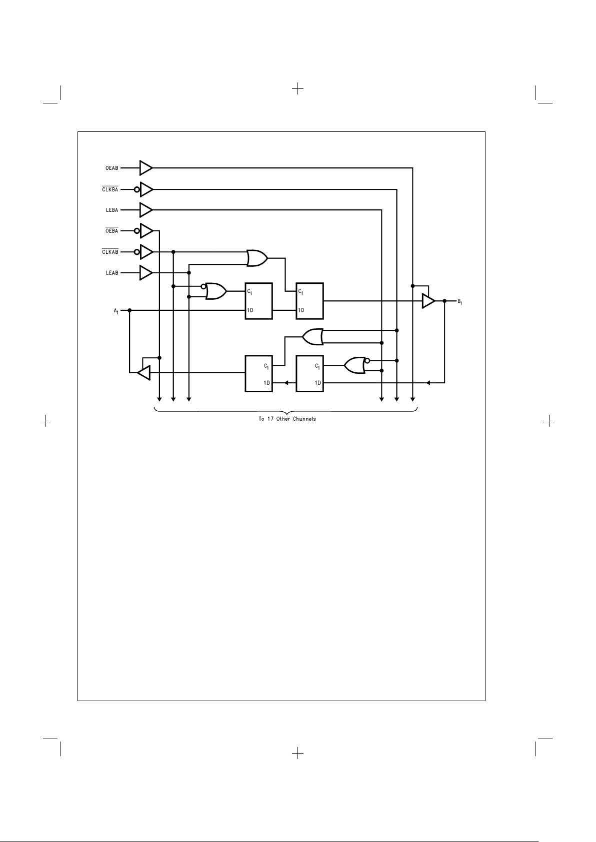
Logic Diagram
DS100225-2
3 www.national.com
PrintDate=1998/07/14 PrintTime=11:08:55 43605 ds100225 Rev. No. 1 cmserv Proof 3
 Loading...