NSC 5962-9684302VXA, 5962-9684301VZA, 5962-9684301VXA Datasheet

TL/H/5713
LM113/LM313 Reference Diode
December 1994
LM113/LM313 Reference Diode
General Description
The LM113/LM313 are temperature compensated, low voltage reference diodes. They feature extremely-tight regulation over a wide range of operating currents in addition to an
unusually-low breakdown voltage and good temperature
stability.
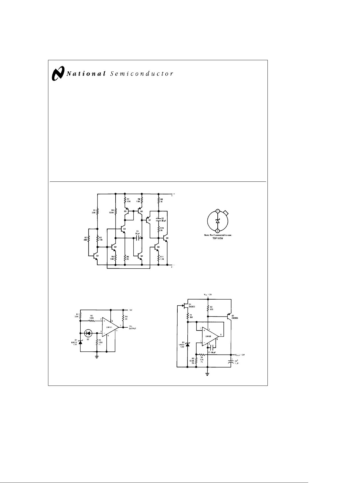
The diodes are synthesized using transistors and resistors
in a monolithic integrated circuit. As such, they have the
same low noise and long term stability as modern IC op
amps. Further, output voltage of the reference depends only
on highly-predictable properties of components in the IC; so
they can be manufactured and supplied to tight tolerances.
Features
Y
Low breakdown voltage: 1.220V
Y
Dynamic impedance of 0.3X from 500 mAto20mA
Y
Temperature stability typically 1% overb55§Cto125§C
range (LM113), 0
§
Cto70§C (LM313)
Y
Tight tolerance:g5%,g2% org1%
The characteristics of this reference recommend it for use in
bias-regulation circuitry, in low-voltage power supplies or in
battery powered equipment. The fact that the breakdown
voltage is equal to a physical property of siliconÐthe energy-band gap voltageÐmakes it useful for many temperature-compensation and temperature-measurement functions.
Schematic and Connection Diagrams
Metal Can Package
Order Number
LM113H, LM113H/883,
LM113-1H, LM113-1H/883,
LM113-2H, LM113-2H/883,
or LM313H
See NS Package Number H02A
TL/H/5713– 1
Typical Applications
Level Detector for Photodiode
Low Voltage Regulator
²
Solid tantalum.
TL/H/5713– 2
C
1995 National Semiconductor Corporation RRD-B30M115/Printed in U. S. A.

Absolute Maximum Ratings
If Military/Aerospace specified devices are required,
please contact the National Semiconductor Sales
Office/Distributors for availability and specifications.
(Note 3)
Power Dissipation (Note 1) 100 mW
Reverse Current 50 mA
Forward Current 50 mA
Storage Temperature Range
b
65§Ctoa150§C
Lead Temperature
(Soldering, 10 seconds) 300
§
C
Operating Temperature Range
LM113
b
55§Ctoa125§C
LM313 0
§
Ctoa70§C
Electrical Characteristics (Note 2)
Parameter Conditions Min Typ Max Units
Reverse Breakdown Voltage
LM113/LM313
I
R
e
1mA
1.160 1.220 1.280 V
LM113-1 1.210 1.22 1.232 V
LM113-2 1.195 1.22 1.245 V
Reverse Breakdown Voltage
0.5 mA
s
I
R
s
20 mA 6.0 15 mV
Change
Reverse Dynamic Impedance
I
R
e
1 mA 0.2 1.0 X
I
R
e
10 mA 0.25 0.8 X
Forward Voltage Drop I
F
e
1.0 mA 0.67 1.0 V
RMS Noise Voltage
10 Hz
sfs
10 kHz
5 mV
I
R
e
1mA
Reverse Breakdown Voltage 0.5 mAsI
R
s
10 mA
15 mV
Change with Current T
MIN
s
T
A
s
T
MAX
Breakdown Voltage Temperature 1.0 mAsI
R
s
10 mA
0.01 %/
§
C
Coefficient T
MIN
s
T
A
s
T
MAX
Note 1: For operating at elevated temperatures, the device must be derated based on a 150§C maximum junction and a thermal resistance of 80
§
C/W junction to
case or 440
§
C/W junction to ambient.
Note 2: These specifications apply for T
A
e
25§C, unless stated otherwise. At high currents, breakdown voltage should be measured with lead lengths less than (/4
inch. Kelvin contact sockets are also recommended. The diode should not be operated with shunt capacitances between 200 pF and 0.1 mF, unless isolated by at
least a 100X resistor, as it may oscillate at some currents.
Note 3: Refer to the following RETS drawings for military specifications: RETS113-1X for LM113-1, RETS113-2X for LM113-2 or RETS113X for LM113.
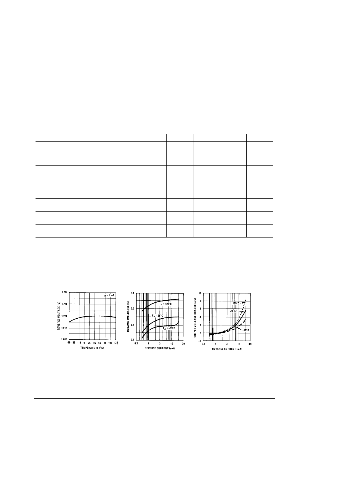
Typical Performance Characteristics
Temperature Drift Reverse Dynamic Impedance Reverse Characteristics
TL/H/5713– 3
2
 Loading...