

Page 1

Programmes After Market Services
Technical Documentation
[NMP Part No.0275514]
NPC-1 Cellular Phones
NPC-1 Issue 1: 10/2001
Issue 1 10/01
Copyrightã 2001 Nokia Corporation All Rights Reserved
Page 2

Programmes After Market Services
Technical Documentation
Amendment Record Sheet
Amendment No Date Inserted By Comments
First Issue 10/2001 JoM
Issue 1 10/01
Copyrightã 2001 Nokia Corporation All Rights Reserved
Page 3

Contents:
Programmes After Market Services
Technical Documentation
NPW-1 Overall Manual Contents
Section 1: Foreword
Section 2: General Information
Section 3: System Module
Section 4: Parts List
Section 5: Product Variants
Section 6: Service Software Instructions
Section 7: Service Tools
Section 8: Assembly & Disassembly Instructions
Section 9: Troubleshooting Instructions
Section 10: Accessories
Section 11: Schematics
Issue 1 10/01
Copyrightã 2001 Nokia Corporation All Rights Reserved
Page 4

Programmes After Market Services
This document is intended for use by qualified service personnel only.
Company Policy
Our policy is of continuous development; details of all technical modifications will be
included with service bulletins.
While every endeavour has been m ade to ensure the accuracy of this document, some
errors may exist. If any errors are found by the reader, NOKIA MOBILE PHONES Ltd.
should be notified in writing.
Please state:
Technical Documentation
IMPORTANT
Title of the Document + Issue Number/Date of publication
Latest Amendment Number (if applicable)
Page(s) and/or Figure(s) in error
Please send to: Nokia Mobile Phones Ltd.
PAMS Technical Documentation
PO Box 86
FIN-24101 SALO
Finland
Issue 1 10/01
Copyrightã 2001 Nokia Corporation All Rights Reserved
Page 5

Programmes After Market Services
Technical Documentation
Warnings and Cautions
Please refer to the phone's user guide f or instructions relating to operation, care and
maintenance including important safety information. Note also the following:
Warnings:
1. CARE MUST BE TAKEN ON INSTALLATION IN VEHICLES FITTED WITH ELECTRONIC ENGINE MANAGEMENT SYSTEMS AND ANTI-SKID BRAKING SYSTEMS. UNDER CERTAIN FAULT CONDITIONS, EMITTED RF ENERGY CAN
AFFECT THEIR OPERATION. IF NECESSARY, CONSULT THE VEHICLE DEALER/
MANUFACTURER TO DETERMINE TH E IMMUNITY OF VEHICLE ELECTRONIC
SYSTEMS TO RF ENERGY.
2. THE HANDPORTABLE TELEPHONE MUST NOT BE OPERATED IN AREAS LIKELY
TO CONTAIN POTENTIALLY EXPLOSIVE ATMOSPHERES EG PETROL STATIONS
(SERVICE STATIONS), BLASTING AREAS ETC.
3. OPERATION OF ANY RADIO TRANSMITTING EQUIPMENT, INCLUDING CELLU-
Cautions:
1. Servicing and alignment must be undertaken by qualified personnel only.
2. Ensure all work is carried out at an anti-static workstation and that an anti-
3. Ensure solder, wire, or foreign matter does not ent er the te lephone as dam-
4. Use only approved components as specified in the parts list.
5. Ensure all components, modules screws and insulators are corre ctly re-fit-
LAR TELEPHONES, MAY INTERFERE WITH THE FUNCTIONALITY OF INADEQUATELY PROTECTED MEDICAL DEVICES. CONSULT A PHYSICIAN OR THE
MANUFACTURER OF THE MED ICAL DEVICE IF YOU HAVE ANY QUESTIONS.
OTHER ELECTRONIC EQUIPMENT MAY ALSO BE SUBJECT TO INTERFERENCE.
static wrist strap is worn.
age may result.
ted after servicing and alignmen t. Ensure all cables a nd wires are repositioned correctly.
Issue 1 10/01
Copyrightã 2001 Nokia Corporation All Rights Reserved
Page 6

Programmes After Market Services
Technical Documentation
This page intentionally left blank.
Issue 1 10/01
Copyrightã 2001 Nokia Corporation All Rights Reserved
Page 7

Programmes After Market Services
NPC-1 Series Transceivers
General Information
Issue 1 10/01 ãNokia Corporation
Page 8

NPC-1
General Information PAMS Technical Documentation
Table of Contents
Page No
NPC-1 Product Selection............................................................................................... 4
Hand portables .............................................................................................................4
Desktop Option ............................................................................................................5
Mobile Holder (MBC-6) Option ..................................................................................6
Product and Module List................................................................................................ 7
Technical Specifications ................................................................................................ 8
General Specifications of Transceiver NPC-1 .............................................................8
Page 2 ãNokia Corporation Issue 1 10/01
Page 9

NPC-1
PAMS Tec hnical Documentation General Information
List of Figures
Page No
Fig 1 Hand portables, Nokia Design and Gradiente Design................................................4
Fig 2 Desktop option............................................................................................................5
Fig 3 Mobile Holder ...........................................................................................................6
Issue 1 10/01 ãNokia Corporation Page 3
Page 10
NPC-1
General Information PAMS Technical Documentation
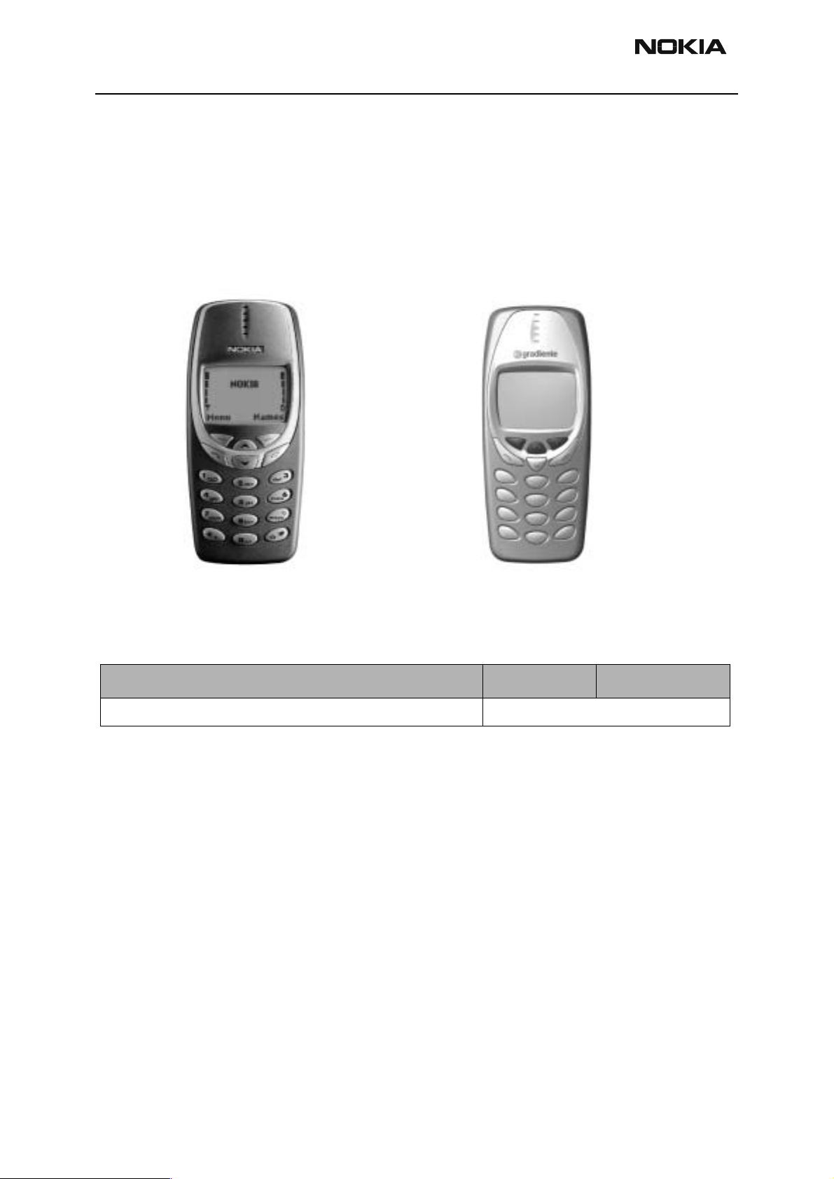
NPC-1 Product Selection
Hand portables
The Nokia 3320 is a TDMA single band (SB), 800MHz + AMPS hand portable telephone.
This document describes the main characteristics of this phone.
Figure 1: Hand portables, Nokia Design and Gradiente Design
Table 1: Transceiver NPC-1
Name: Type Code: Material Code:
Transceiver (See Product Variants)
Page 4 ãNokia Corporation Issue 1 10/01
Page 11
NPC-1
PAMS Tec hnical Documentation General Information
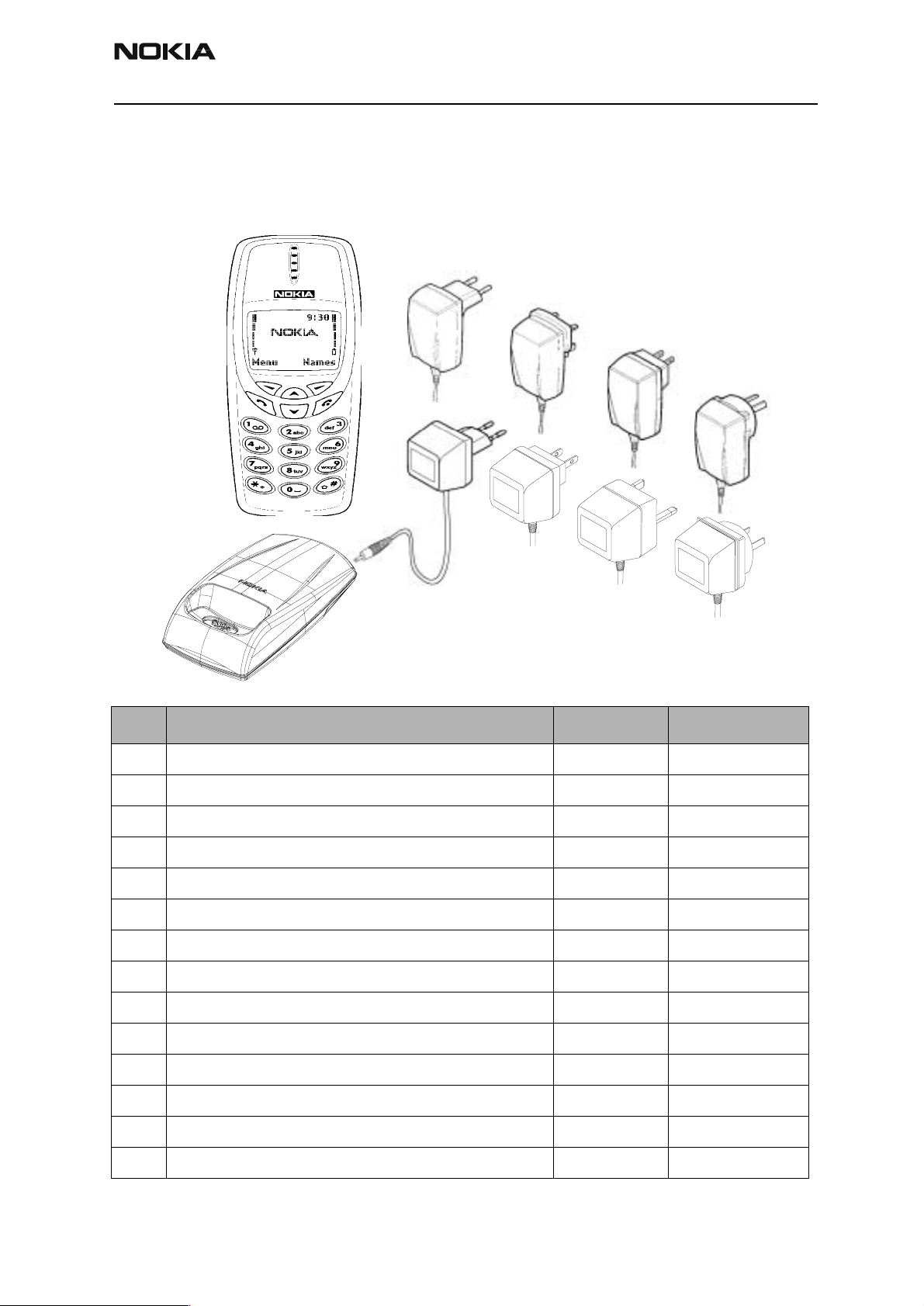
Desktop Option
The desktop option allows the user to charge the phone from the mains.
Figure 2: Desktop option
1.
3.
ACP-7E
2.
ACP-8E
ACP-8K
7.
ACP-8X
8.
ACP-8U
ACP-8C
9.
ACP-8A
10.
4.
ACP-7C
ACP-7U
5.
ACP-7H
ACP-7X
6.
ACP-7A
Item Name: Type Code: Material Code:
1. Transceiver (See Product Variants)
2 Desk stand DCV-10 0675229
3. AC Travel Charger (Euro plug) 207-253 Vac ACP-7E 0675144
4. AC Travel Charger (US plug) 108-132 Vac ACP-7U 0675143
AC Travel Charger (US plug ) 198-242 Vac ACP-7C 0675158
5. AC Travel Charger (UK plug) 207-253 Vac ACP-7X 0675145
AC Travel Charger (UK plug ) 18 0-220 Vac ACP-7H 0675146
6. AC Travel Charger (Australia plug) 216-264 Vac ACP-7A 0675148
7. Performance Travel Charger Euro plug 90-264 Vac ACP-8E 0675195
Performance Travel Charger Korea plug 90-264 Vac ACP-8K 0675199
8. Performance Travel Charger UK plug 90-264 Vac ACP-8X 0675197
9. Performance Travel Charger US plug 90-264 Vac ACP-8U 0675196
Performance Travel Charger China plug 90-264 Vac ACP-8C 0675211
10. Performance Travel Charger Australia plug 90-264 V a c AC P -8A 0675214
Issue 1 10/01 ãNokia Corporation Page 5
Page 12
NPC-1
General Information PAMS Technical Documentation
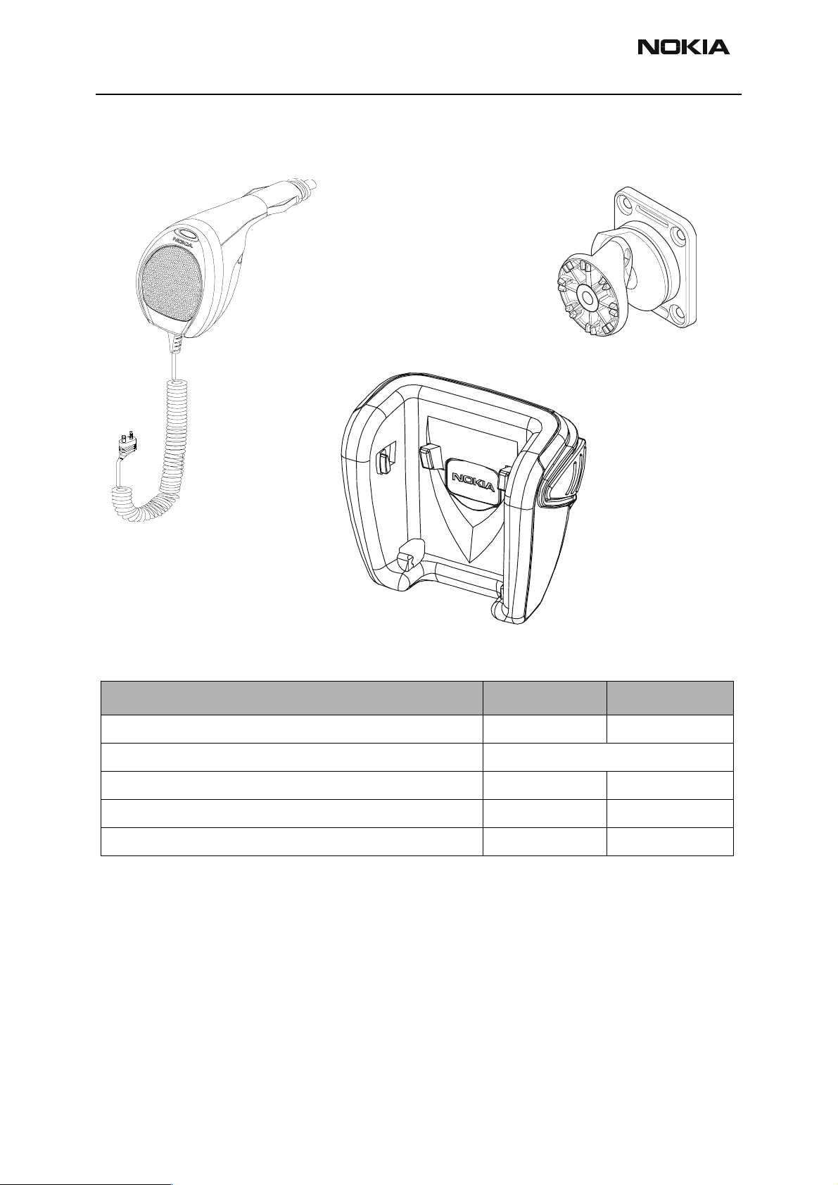
Mobile Holder (MBC-6) Option
Figure 3: Mobile Holder
Item Name: Type Code: Material Code:
Mobile Holder MBC-6 0650026
Transceiver (Not included) (See Product Variants)
Swivel Mount HHS-9 0620037
Hands Free Microphone HFM-8 0690016
Hands Free Cigarette Lighter Charger PPH-1 0675182
Page 6 ãNokia Corporation Issue 1 10/01
Page 13
NPC-1
PAMS Tec hnical Documentation General Information
Product and Module List
Unit/Type: Product Code:
Transceiver NPC-1 See Product Variants
Standard Battery BLC-2 (Li-ION ) 850 mAh) 0670343
Standard Battery BMC-2 (NiMh) 900 mAh) 0670323
Standard Battery BMC-3(NiMh ) 850 mAh 0670324
AC Travel Charger ACP-7E (EURO) 207-253 Vac 0675144
AC Travel Charger ACP-7U (US) 108-132 Vac 0675143
AC Travel Charger ACP-7C (US) 198-242 Vac 0675158
AC Travel Charger ACP-7X (UK) 2 07-253 Vac 0675145
AC Travel Charger AC P - 7H ( UK) 180-220 Vac 0675146
AC Travel Charger ACP-7A (AUS) 216-264 Vac 0675148
Performance Travel Charger ACP-8E (EURO) 90-264 Vac 0675195
Performance Travel Charger ACP-8K (KOREA) 90-264 Vac 0675199
Performance Travel Charge r AC P - 8X (UK) 90-264 Vac 0675197
Performance Travel Charg e r AC P - 8U (US) 90-264 Vac 0675196
Performance Travel Charger ACP-8C (CHINA) 90-264 Vac 0675211
Performance Travel Charger ACP-8A (AUS) 90-264 Vac 0675214
Headset HDE-2 0694075
Headset HDC-5 0694059
Loopset LPS-3 0630244
Battery Charging Stand DDC-1 0675243
Desk Stand DCV-10 0675229
Swivel Mount HHS-12 0620054
HF Microphone HFM-8 0690016
Plug & Play HF Cigarette Lighter Charger PPH-1 0675182
Cigarette Lighter Charger LCH-8 0675231
Cigarette Lighter Charger LCH-9 0675120
Issue 1 10/01 ãNokia Corporation Page 7
Page 14
NPC-1
General Information PAMS Technical Documentation
Technical Specifications
General Specifications of Transceiver NPC-1
Parameter Unit
Cellular System TDMA800 + AMPS
RX frequency band 869.01... 893.97 MHz
TX frequency band 824.01... 848.97MHz
Output power -5...+28 dBm / 0.3 mW... 630mW
Number of RF channels 832
Channel spacing 30 kHz
Page 8 ãNokia Corporation Issue 1 10/01
Page 15

Programmes After Market Services
NPC-1 Series Transceivers
System Module
Issue 1 10/01 ãNokia Corporation
Page 16

NPC-1
System Module PAMS Technical Documentation
Table of Contents
Page No
System Module ...............................................................................................................1
Abbreviations................................................................................................................. 6
Transceiver NPC-1......................................................................................................... 8
Introduction ..................................................................................................................8
Operational Modes.................................................................................................... 9
Environmental Specifications ......................................................................................9
Normal and extreme voltages.................................................................................... 9
Temperature Conditions............................................................................................ 9
Engine Module............................................................................................................. 11
Baseband Module ......................................................................................................11
UEM ..........................................................................................................................11
Introduction to UEM............................................................................................... 11
Regulators................................................................................................................ 12
RF Interface............................................................................................................. 13
Charging Control..................................................................................................... 13
Digital Interface....................................................................................................... 13
Audio Codec............................................................................................................ 14
UI Drivers................................................................................................................ 14
IR interface.............................................................................................................. 14
AD Converters......................................................................................................... 14
UPP ............................................................................................................................14
Introduction............................................................................................................. 14
Blocks...................................................................................................................... 14
Flash Memory ............................................................................................................15
Introduction............................................................................................................. 15
User Interface Hardware .............................................................................................. 15
LCD ...........................................................................................................................15
Introduction............................................................................................................. 15
Interface................................................................................................................... 15
Keyboard ....................................................................................................................15
Introduction............................................................................................................. 15
Power Key............................................................................................................... 16
Keys......................................................................................................................... 16
Lights .........................................................................................................................16
Introduction............................................................................................................. 16
Interfaces................................................................................................................. 17
Technical Information............................................................................................. 17
Vibra ..........................................................................................................................17
Introduction............................................................................................................. 17
Interfaces................................................................................................................. 17
Audio HW.................................................................................................................... 18
Earpiece .....................................................................................................................18
Introduction............................................................................................................. 18
Microphone ................................................................................................................18
Introduction............................................................................................................. 18
Buzzer ........................................................................................................................18
Introduction............................................................................................................. 18
Page 2 ãNokia Corporation Issue 1 10/01
Page 17

NPC-1
PAMS Technical Documentation System Module
Battery.......................................................................................................................... 18
Phone Battery .............................................................................................................18
Introduction............................................................................................................. 18
Interface................................................................................................................... 18
Battery Connector ......................................................................................................19
Accessories Interface ................................................................................................... 20
System connector .......................................................................................................20
Introduction............................................................................................................. 20
Interface................................................................................................................... 20
Technical Information............................................................................................. 21
PPH-1 Handsfree .......................................................................................................21
Introduction............................................................................................................. 21
Interface................................................................................................................... 22
IR module ..................................................................................................................22
Introduction............................................................................................................. 22
Interface................................................................................................................... 22
Technical Information............................................................................................. 22
Charger IF ..................................................................................................................22
Introduction............................................................................................................. 22
Interface................................................................................................................... 23
Test Interfaces.............................................................................................................. 23
Production Test Pattern ..............................................................................................23
Other Test Points .......................................................................................................23
EMC............................................................................................................................. 24
General .......................................................................................................................24
BB Component and Control IO Line Protection .......................................................24
Keyboard lines......................................................................................................... 24
C-Cover................................................................................................................... 24
PWB........................................................................................................................ 24
LCD......................................................................................................................... 25
Microphone ............................................................................................................. 25
EARP....................................................................................................................... 25
Buzzer...................................................................................................................... 25
IRDA....................................................................................................................... 25
System Connector Lines.......................................................................................... 25
Battery Connector Lines.......................................................................................... 25
MBUS and FBUS.................................................................................................... 25
Transceiver Interfaces.................................................................................................. 26
BB - RF Interface Connections .................................................................................26
BB Internal Connections ............................................................................................28
UEM Block Signal Description............................................................................... 28
UPP Block signals................................................................................................... 33
MEMORY Block Interfaces.................................................................................... 36
IR Block Interfaces.................................................................................................. 37
Audio Interfaces...................................................................................................... 37
Key/Display blocks................................................................................................. 39
Baseband External Connections.............................................................................. 40
Test Pattern for Production Tests............................................................................ 41
Issue 1 10/01 ãNokia Corporation Page 3
Page 18

NPC-1
System Module PAMS Technical Documentation
RF Module ................................................................................................................... 42
Requirements .............................................................................................................42
Design ........................................................................................................................42
Software Compensations ...........................................................................................42
Main Technical Characteristics .................................................................................43
RF Frequency Plan.................................................................................................. 43
DC Characteristics .....................................................................................................43
Power Distribution Diagram ................................................................................... 43
Regulators................................................................................................................ 45
Receiver .....................................................................................................................45
AMPS/TDMA 800 MHz Front End........................................................................ 47
Frequency Synthesizers .............................................................................................48
Transmitter .................................................................................................................49
Common IF ............................................................................................................. 49
Cellular Band........................................................................................................... 49
Power Control ......................................................................................................... 49
Antenna Circuit....................................................................................................... 50
RF Performance....................................................................................................... 50
Antenna ........................................................................................................................50
Page 4 ãNokia Corporation Issue 1 10/01
Page 19

NPC-1
PAMS Technical Documentation System Module
List of Figures
Page No
Fig 1 Interconnecting Diagram............................................................................................8
Fig 2 System Block Diagram (simple) ................................................................................11
Fig 3 Placement of keys.......................................................................................................16
Fig 4 Battery Connection Diagram......................................................................................19
Fig 5 BMC-2 Battery contacts (BMC-3, BLC-2 have same interface). ..............................19
Fig 6 System Connector.......................................................................................................20
Fig 7 Accessory Detection / External Audio .......................................................................21
Fig 8 4-wire, fully differential headset connector pin layout...............................................22
Fig 9 Top View of Production Test Pattern.........................................................................23
Fig 10 Test points Located Between UEM and UPP...........................................................24
Fig 11 RF Frequency Block Plan.........................................................................................43
Fig 12 Power distribution ....................................................................................................44
Issue 1 10/01 ãNokia Corporation Page 5
Page 20

NPC-1
System Module PAMS Technical Documentation
Abbreviations
ACCH Analog Control Channel
A/D Analog to Digital conversion
AMPS Advanced Mobile Phone System
ANSI American National Standards Institute
ASIC Application Specific Integrated Circuit
AVCH Analog V oice Channel
BB Base Band
CSD Circuit Switched Data
CSP Chipped Scale Package. The same as uBGA.
CTIA Cellular Telecommunications Industry Association
D/A Digital to Analog conversion
DCCH Di gi tal Control Channel
DSP Digital Signal Processing
DTCH Digital Traffic Channel
EDMS El ectronic Data Management System
EFR Enhanced Full Rate (codec)
FCC Federal Communications Commission
IR Infrared
IrDA Infrared Data Association
IrMC Infrared Mobile Communications
IrOBEX IrDA Object Exchange Protocol
IS Interim Standard
ISA Intelligent Software Architecture
LED Light Emitting Diode
MCU Micro Control Unit / Master Control Unit
MO/MT Mobile Originated/Mobile Terminated (SMS)
OOR Out Of Range (mode)
OTA Over The Air (+ service like Programming etc.)
PC Personal Computer (PC Suite = PC program for phone memory function support)
PWB Printed Wired Board
PWM Pulse Width Modulation
RF Radio Frequency
SAR Specific Absorption Rate
SCF Software Component Factory
SMD Surface Mount Device
SMS Short Message Service
SPR Standard Product Requirement
TDD Text Device for the Deaf
Page 6 ãNokia Corporation Issue 1 10/01
Page 21

NPC-1
PAMS Technical Documentation System Module
TDMA Time Division Multiple Access. Here: US digital cellular system.
TIA Telecommunications Industry Association
TTY Teletype
UEM Universal Energy Management, a Baseband ASIC.
UPP Universal Phone Processor, a Baseband ASIC.
VCTCXO Vol tage Controlled temperature Compensated Crystal Oscill ator
WAP Wireless Application Protocol (Browser)
Issue 1 10/01 ãNokia Corporation Page 7
Page 22
NPC-1
1
2
3
4
5
7
8
System Module PAMS Technical Documentation
Transceiver NPC-1
Introduction
The NPC-1 is a single band transceiver unit designed for TDMA800 networks. The transceiver consists of the engine module (WS8) and the various assembly parts.
The transceiver has a full graphic display and the user interface is based o n a jack style
UI with two soft keys. An internal antenna is used in the phone, and there is no connection to an external antenna. The transceiver also has a low leakage tolerant earpiece and
an omnidirectional microphone that provides excellent audio quality.
An integrated infrared (IR) link provides connec tion between two NPC-1 transcei vers or
between a transceiver and a PC (internal da ta), or a transceiver and a printer.
Figure 1: Interconnect ing Diagram
TRANSCEIVER
ANT
EXT
RF
Ostrich
LCD DRIVER
B & W
display
BACKLIGHT
BACKLIGHT
✉
RF
☎
6
9
0#
ENGINE
BB
USER INTERFACE
EARPIECE
AUDIO
(discr)
BUZZER
VIBRA
RTC
BACK-UP
BSI
BTemp
MIC
Ext. Aud io
Accessories
BATTER Y
JTAG
Prod.TEST I/F
INF R A R E D
Module
CHARGER
Page 8 ãNokia Corporation Issue 1 10/01
Page 23

NPC-1
PAMS Technical Documentation System Module
Operational Modes
Below is a list of the phone’s different ope rational modes:
1 Power Off mode
2 Normal Mode (include various Active and Idle states):
• Analog Modes (800 MHz only):
•Analog Control Channel, ACCH
•Analog Voice Channel, AVCH
• Digital Modes (800 MHz):
•Control Channel, DCCH
•Digital Voice Channel, S-DTCH
•Digital Data Channel, D-DTCH
3 Sleep and OOR modes (both Analog and Digital)
4Local mode
5 Test mode
Environmental Specifications
Normal and extreme voltages
Voltage range:
• nominal battery voltage: 3.6 V
• maximum battery voltage: 5.0 V
• minimum battery voltage: 3.1 V
Temperature Conditions
Temperature range:
• ambient temperature: -30 - + 60 ×C
• PWB temperature: -30 - +85 ×C
• storage temperature range: -40 - + 85 ×C
All of the EIA/TIA-136-270A requirements are not exactly specified over the temperature
Issue 1 10/01 ãNokia Corporation Page 9
Page 24

NPC-1
System Module PAMS Technical Documentation
range. For example, the RX sensitivity requirement is 3dB lower over the –30 - +60 °C
range.
Page 10 ãNokia Corporation Issue 1 10/01
Page 25
NPC-1
V
A
y
UI
T
T
A
X
X
PAMS Technical Documentation System Module
Engine Module
Baseband Module
The core part of the transceiver’s baseband (figure 1) consists of 2 ASICs, the UEM and
UPP, and flash memory. The following sections illustrate and explain these parts in detail.
Figure 2: System Block Diagram (simple)
PA suppl
SAFARI
RFIC CTRL
RFCLK
19.44MHz
UPP
MEMADDA
MEMCON
FLASH
RF Supplies
RF RX/T
PURX
RF RX/T
SLEEPCLOCK
32kHz
CBUS/DBUS
UDIO
BB Supplies
KLIGHT/ DLIGH
PWR ON
BASEBAND
UEM
EXTERNAL AUDIO
CHARGER CONNECTION
IR
EAR
MIC
BUZZER
IBR
BATTERY
System Connector
UEM
Introduction to UEM
UEM is the Universal Energy Management IC for digital hand portable phones. In addition to energy management, it performs all the base band’s mixed-signal functions.
Most UEM pins have 2kV ESD protection, and those signals considered to be more easily
exposed to ESD, have 8kV protection within the UEM. These kinds of signals are (1) all
audio signals, (2) headset signals, (3) BSI, (4) Btemp, (5) Fbus and (6) Mbus signals.
Issue 1 10/01 ãNokia Corporation Page 11
Page 26
NPC-1
System Module PAMS Technical Documentation
Regulators
The UEM has six regulators for baseband power supplies and seven regulators for RF
power supplies. The VR1 regulator has two outputs: (1) VR1a and (2) VR1b. In addition to
these, there are two current generators - IPA1 and IPA2 - for biasing purposes.
A bypass capacitor (1uF) is required for each regulator output to ensure stability.
Reference voltages for regulat ors require exter nal 1uF capacitors. Vref25RF is the refer-
ence voltage for the VR2 regulator, Vref25BB is the reference voltage for the VANA,
VFLASH1, VFLASH2, VR1 regulators, Vref278 is the re ference voltage for the VR3, VR4,
VR5, VR6, VR7 regulators, and VrefRF01 is the reference voltage for the VIO, VCORE regulators and for the radio frequency (RF).
Table 1: UEM Regulators
BB RF Current
VANA: 2.78Vtyp 80mAmax VR1a:4.75V 10mAmax
VR1b:4.75V
Vflash1: 2.78Vtyp 70mAmax IPA2: 0-5mA
Vflash2: 2.78Vtyp
40mAmax
VSim: 1.8/3.0V 25mAmax VR3:2.7 8V 20m A
VIO: 1.8Vtyp
150mAmax
Vcore: 1.0-1.8V
200mAmax
VR2:2.78V 100mAmax
VR4: 2.78V 50mAmax
VR5: 2.78V 50mAmax
VR6: 2.78V 50mAmax
VR7: 2.78V 45mAmax
IPA1: 0-5mA
The VANA regulator supplies the baseband’s (BB) internal and ex ternal analog circuitry.
It is disabled in the Sleep mode.
The Vflash1 regulator supplie s the LCD, the IR-module and the digital parts of th e UEM
and Safari asic. It is enabled during startup an d goes into the low Iq-mode when in the
Sleep mode.
The VIO regulator supplies both the external and internal l ogic circuitries. It is used by
the LCD, flash, bluetooth and UPP. The regulator goes into the low Iq-mode when in the
Sleep mode.
The VCORE regulator supplies the D SP and the core part of the U PP. The voltage is programmable and the startup default is 1.5V. The regulator goes into the low Iq-mode
when in the Sleep mode.
The VSIM regulator supplies the SIM card. NOT USED IN NPC-1.
Page 12 ãNokia Corporation Issue 1 10/01
Page 27

NPC-1
PAMS Technical Documentation System Module
The VR1 regulator uses two LDO s and a charge pump. The charge pump requires one
external 1uF capacitor in the Vpump pin and a 220nF flying capacitor between the CCP
and CCN pins. In practice, the 220nF flying capacitor is f ormed by 2 x 100nF capacitors
that are parallel to each other. The VR1 regulator is used by the Safari RF ASIC.
The VR2 regulator is used to supply the (1) external RF parts, (2) lower band up converter, (3) TX power detector module and (4) Safari. In light load situatio ns, the VR2 regulator can be set to the low Iq-mode.
The VR3 regulator supplies the VCTCXO and Safari in the RF. It is always enabled when
the UEM is active. When the UEM is in the Sleep mode, the VR3 is disabled.
The VR4 regulator supplies the RX frontends (LNA and RX mixers).
The VR5 regulator supplies the lower band PA. In light load situations, the VR5 regulator
can be set to the low Iq-mode.
The VR6 regulator supplies the higher band PA and TX amplifier. In light load situations,
the VR6 regulator can be set to the low Iq-mode.
The VR7 regulator supplies the VCO and Safari. In light load situations, the VR7 regulator
can be set to the low Iq-mode.
The IPA1 and IPA2 are programmable current gener ators. A 27kW/1%/100ppm external
resistor is used to improve the accuracy of the output current. The IPA1 is used by the
lower PA band and IPA2 is used by the higher PA band.
RF Interface
The interface between the baseband and the RF section is also handled by the UEM. It
provides A/D and D/A conversion of the in-pha se and quadrature receive and transmit
signal paths. It also provides A/D and D/ A conve rsions of receiv ed and transmitte d audio
signals to and from the UI section. The UEM supplies the analog AFC signal to the RF section, according to the UPP DSP digital control.
Charging Control
The CHACON block of the UEM asics controls charging. The needed functions for the
charging controls are the (1) pwm-controlled battery charging switch, (2) charger-monitoring circuitry, (3) battery voltage monitori ng circuitry and (4) RTC supply circuitry for
backup battery charging (Not used in NPC-1). In addition to these, external component s
are needed for EMC protection of the charger input to the baseband module.
Digital Interface
Data transmission between the U EM and the UPP is impleme nted using two seri al connections, DBUS (programmable clock) for DSP and CBUS (1.0MHz GSM and 1.08MHz
TDMA) for MCU. The UEM is a dual voltage circuit: the digital parts are run from 1.8V
and the analog parts are run from 2.78V. The Vbat (3,6V) voltage regulators's input is
also used.
Issue 1 10/01 ãNokia Corporation Page 13
Page 28

NPC-1
System Module PAMS Technical Documentation
Audio Codec
The baseband supports two external microphone input ar eas and one external ea rphone
output. The input can be taken from an internal microphone, a headset microphone or
from an external microphone signal source through a headset connector. The output for
the internal earpiece is a dual-ended type output, and the dif ferential output is capable
of driving 4Vpp to the earpiece with a 60 dB minimum signal as the total distortion ratio.
The input and output signal source se lection and gain control is performed inside the
UEM Asic, according to the c ontrol messages from the UPP. A buzzer a nd an external
vibra alert control signal are gener ated by the UEM with separate PWM outputs.
UI Drivers
There is a single output driver for the buzzer, vibra, display and keyboard l eds an d the IR
in the side of the UEM. These generate PWM square wave for the various devices.
IR interface
The IR interface is designed and implemented into th e UEM. The low frequency mode of
the IR module covers speeds up to 115.2 kbit/s. The device (Vis hay) transceivers integrate
a sensitive receiver and a built-in power driver. The combination of a thin, long resistive
and inductive wiring should be avoided. The input (Txd, SD/M ode) and the output Rxd
should be directly coupled to the I/O circuit. The VBAT regulator supplies the power to
transmit the led and serial resistor limits’ current. Upon rece ivi ng infra red data to IR led,
it goes straight to the UEM via the RXD line . The Vflash1 is the power supply f or the IR
module, except for transmission.The IR module has one control pin to control the shut
down. The control lever shifter is used to change the proper voltage for shutdown to the
IR module from the UPP.
AD Converters
The UEM is equipped with a 11-channel analog to digital converter. Some AD converter
channels (LS, KEYB1-2) are not used in NPC-1. The AD converters are calibrated in the
production line.
UPP
Introduction
NPC-1 uses the UPPv4M ASIC. The RAM size is 4M. The processor architecture consists of
both the DSP and the MCU processors.
Blocks
The UPP is internally partitioned into two main parts: (1) the Brain and (2) the Body.
1 The Processor and Memory System (that is, the Processor cores, Mega-cells,
internal memories, perip herals and external memory inter face) is known as the
Brain.
The Brain consists of the following blocks: (1) the DSP Subsystem (DSPSS), (2) the
MCU Subsystem (MCUSS), (3) the emulation control EMUCtl, (4) the program/
data RAM PDRAM and (5) the Brain Peripherals–subsystem (BrainPer).
Page 14 ãNokia Corporation Issue 1 10/01
Page 29

NPC-1
PAMS Technical Documentation System Module
2 The NMP custom cellular logic functions are known as the Body.
The Body contains interfaces and functions needed fo r interfacing other baseband and RF parts. The body consists of, fo r example, the following sub-blocks:
(1) MFI, (2) SCU, (3) CTSI , (4) RxModem, ( 5) Acc IF, (6) UIF, (7) C oder, (8) BodyIF, (9)
PUP.
Flash Memory
Introduction
The NPC-1 transceiver uses a 32 Mbit f lash as its external memory. The VIO regulator is
used as a power supply for normal in-system op eration. An accelerated program/erase
operation can be obtained by supplying Vpp of 12 volt to the flash device.
The device has two read modes: asynchronous and burst. The Burst read mode is utilized
in NPC-1, except for the start-up, when the asynchronous read mode is used for a short
time.
User Interface Hardware
LCD
Introduction
NPC-1 uses a black & white GD46 84x48 full dot matrix graphical display. There are two
suppliers for this LCD: Seiko Epson and P hilips. The LCD module includes the LCD glass,
the LCD COG-driver, an elastomer connector and a metal frame. The LCD module is
included in the lightguide assembly module.
Interface
The LCD is controlled by the UI SW and the control signals are from the UPP asic. The VIO
and Vflash1 regulators supply the LCD with power.
The LCD has an internal voltage booster and a booster capacitor is required between
Vout and GND.
Pin 3 (Vss9) is the LCD driver’s ground and Pin 9 (GND) is used to ground the metal
frame.
Keyboard
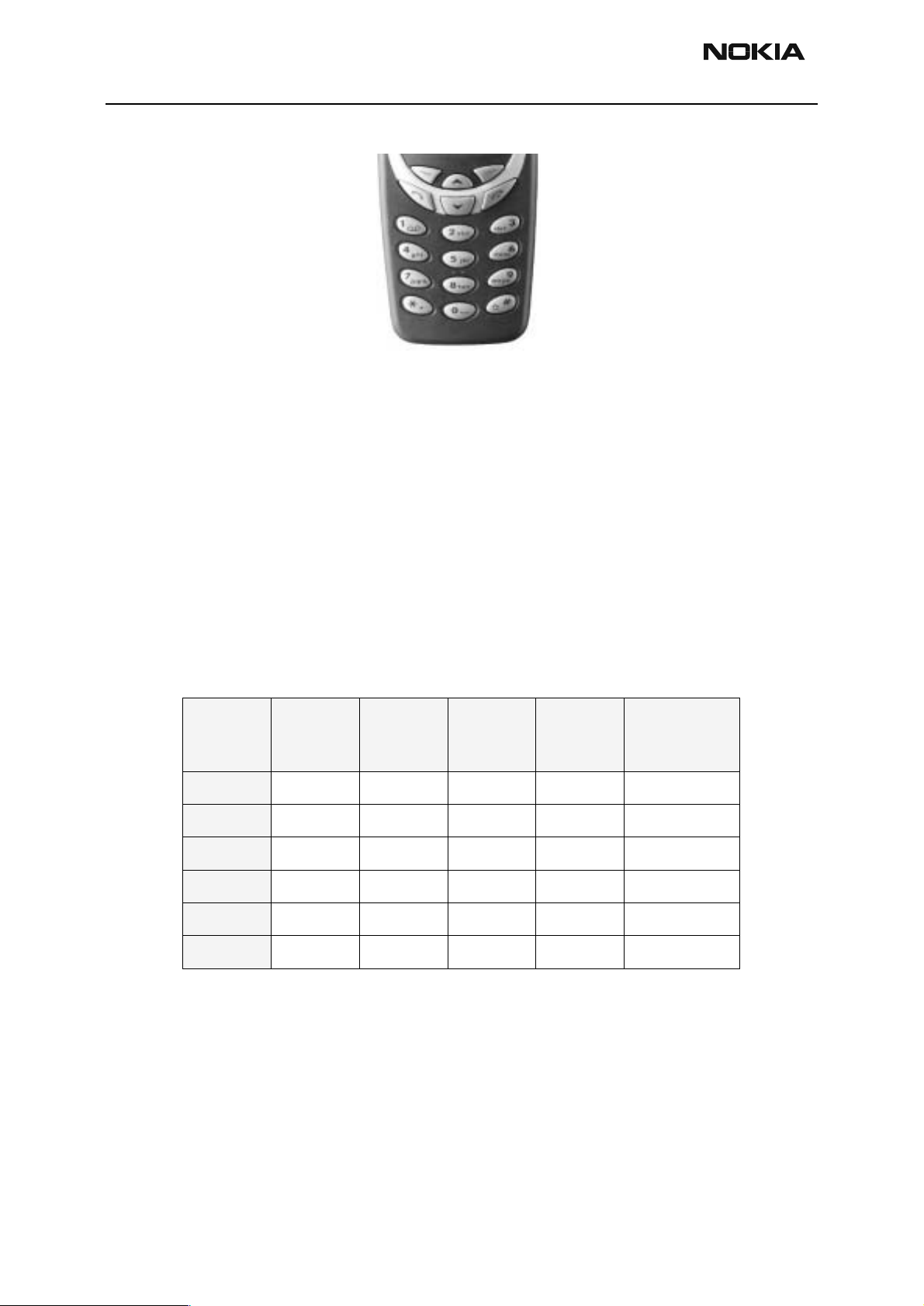
Introduction
The NPC-1 keyboar d styl e fol lows the Nokia Jack style , withou t side keys for vol ume co ntrol. The PWR key is integrated so that it is part of the IR window an d located on top of
the phone.
Issue 1 10/01 ãNokia Corporation Page 15
Page 30
NPC-1
System Module PAMS Technical Documentation
Figure 3: Placement of keys.
Power Key
All signals for the keyboard come from the UPP asic, except PWRONX line for the power
key signal which is connect ed dir ectly to t he U EM. The pr essing o f the PWR k ey gro und s
the PWRONX line and the UEM generate s an inter rupt to U OO, which is then re cognized
as a PWR key press.
Keys
Other keys are detected so that w hen a key is pressed down, the metal dome connects
one S-line and one R-line of the UPP to the GND and creat es an interrupt for the SW.
This kind of detection is also known as metaldome detection. The matrix of how lines are
connected and which lines are used for differen t keys is described in the Table 1. The Sline S0 and R-line R5 are not used at all.
Table 2: Matrix of Key Detection Lines
S0 S1 S2 S3 S4
Returns /
Scans
R0 NC NC Send End NC
R1 NC Soft left Up Down Soft right
R2 NC 1 4 7 *
R3 NC 2 5 8 0
R4 NC 3 6 9 #
R5 NC NC NC NC NC
where NC = Not Connected
Lights
Introduction
NPC-1 has 10 LEDs for lighting purposes. Six of them are for the keyboard and four for
the display. The LED type is Osram LGM470, green light emitting and SMD through hole
mounted.
Page 16 ãNokia Corporation Issue 1 10/01
Page 31

NPC-1
PAMS Technical Documentation System Module
Interfaces
The display lights are controlled by a Dlight signal from the UEM. The Dlight output is the
PWM signal, which is used to control the average current going through the LEDs. When
the battery voltage changes, the new PWM v alue is written onto the PWM register. In
this way, the brightness of the lights remains the same with all battery voltages within
range. The frequency of the signal is fixed at 128Hz.
The keyboard lights are controlled by the Klight signal from the UEM. The Klight output is
also a PWM signal and is used in the same way as Dlight.
Technical Information
Each LED requires a hole in t he PWB, in which the body of the LED locates in hole and
terminals are soldered on the component side of the module PWB. The LEDs have a white
plastic body around the diode, and this directs the emitted light better to the UI-side.
The current for the LCD lights is limited by the resistor between the Vbatt and LEDs. For
the keyboard lights there are resistors in parallel.
Vibra
Introduction
The vibra is located on the D-cover and is connected by spring connectors on the bottom
left-hand side of the engine. The vibra motor is supplied by Namiki.
Interfaces
The vibra is controlled by the PWM signal VIBRA from the UEM. With this signal, it is
possible to control both the frequency and pulse width of the signal. The pulse widt h is
used to control the current when the bat tery vol tage changes. Wit h the freque ncy control, it is possible to search for the optimum frequency to have silent and efficient vibrating.
Table 3: Electrical Parameters
Parameter Requirement Unit
Rated DC Voltage 1.3 V
Rated speed
Rated current
9500 ±3000
115 ±20
rpm
mA
Starting current
Armature resist ant 8.6 ohm
Rated DC voltage being able to use 1.2 to 1.7 V
Starting DC voltage min. 1.2 V
150 ±20
mA
Issue 1 10/01 ãNokia Corporation Page 17
Page 32

NPC-1
System Module PAMS Technical Documentation
Audio HW
Earpiece
Introduction
The Philips Speaker System 13mm speaker capsule is used in NPC-1.
The speaker is a dynamic one. It is very sensitive and capable of producing relatively high
sound pressure also at low frequencies. The speaker capsule and the mechanics around it
together make the earpiece.
Microphone
Introduction
The microphone is an electret microphone with an omnidirec tional polar pattern. It consists of an electrically polarized membrane and a metal electrode which form a capacitor.
Air pressure changes (for example, sound) moves the membrane, which causes voltage
changes across the capacitor. Because the capacitance is t ypically 2 pF, a FET buffer is
needed inside the microphone capsule for the signal generated by the capacitor. Because
of the FET, the microphone needs a bias voltage.
The microphone manufacturers for the NPC-1 transceiver are Matsushita and Hosi den.
Buzzer
Introduction
The operating principle of the buzzer is magnetic. The diaphragm of the buzzer is made
of magnetic material and it is located in a magnetic f ield created by a perm anent magnet. The winding is not attached to the diaphragm, as is the case with the speaker. The
winding is located in the magnetic circuit so tha t it can alter the magnetic field o f the
permanent magnet, thus changing the magnetic force affecting the diaphragm. The
buzzer's useful frequency range is approximately from 2 kHz to 5kHz.
The Buzzer manufacturer for the NPC-1 transceiver is Star.
Battery
Phone Battery
Introduction
The BMC-2 battery (Ni-MH 640mAh) is be used in the NPC-1 transceiver by default. It is
also possible to use the BMC-3 (Ni-MH 900mAh) and BLC-2 (Li-ion 850mA) batteries.
Interface
The battery block contains NTC and BSI resistors for tempe rature measur emen t and battery identification. The BSI fixed resistor value indicates the chemistry and default
Page 18 ãNokia Corporation Issue 1 10/01
Page 33

NPC-1
UEM
Ni-MH
VBATT
GND
BTEMP
Battery
1 (+)
2(BSI)
3(BTEMP)
4(GND)
PAMS Technical Documentation System Module
capacity of a battery. The NTC-resistor measures the battery temperature. Temperature
and capacity information is needed for charge control. These resistors are connected to
BSI and BTEMP pins of the battery connector. The phone has pull-up resistors for these
lines so that they can be re ad by A/D inputs in the phone (see the figure below). Serial
resistors in the BSI and BTEMP lines are f or ESD protection. Both lines also have spark
caps to prevent ESD.
Figure 4: Battery Connection Di agram
C220
1n
C217
1n
R202/1
100k
R205/1
10k
R205/2
10k
VFLASH1VANA VBAT
R202/4
100k
C100
10p
connector
BSI
OVERCHARGE/
OVERDISCHARGE
PROTECTION
The batteries have a specific red line, which indicates if the battery has been subjected to
excess humidity. The batteries are delivered in the protection mode, which gives longer
storage time. The voltage seen in the outer terminals is zero (or floating), and the battery
is activated by connecting the charge r. The battery has internal protection for overvoltage and overcurrent.
Figure 5: BMC-2 Battery contacts (BMC-3, BLC-2 have same interface).
Battery Connector
NPC-1 uses the spring type battery connector. This makes the phone easier to assemble
Issue 1 10/01 ãNokia Corporation Page 19
Page 34

NPC-1
PWMOUT(GND)
System Module PAMS Technical Documentation
in production and the connection between the battery and the PWB is more reliable. The
battery connector is manufactured by Molex.
Table 4: Battery Connector Interface
# Signal
name
1 VBAT (+)
2 BSI BSI
3 BTEMP BTEMP
4 GND GND GND GND
Connected from - to Batt.
(batt.)
(batt.)
(batt.)
VBAT I/O Vbat 3.0-5.1V Battery
UEM Out Ana Battery size
UEM Out Ana 40mA/
Accessories Interface
System connector
Introduction
NPC-1 uses accessories via a system connector.
I/O
Signal properties
A/D--levels--freq./timing
Gns
Switch
400mA
Description /
Notes
voltage
indicator
Battery
temperature
indicator
Ground
Interface
The interface is supported by fully differential 4-wire (XMICN, XMICP, XEARN and
XEARP) accessories. NPC-1 supports the HDC-5 headset, LPS-3 loopset and the PPH-1
car kit.
Figure 6: System Connector
GND
VIN
XMICN
XEARN
MICP
XMICP
XEARP
HEADINT
MICN
Page 20 ãNokia Corporation Issue 1 10/01
Page 35

NPC-1
MicGnd
PAMS Technical Documentation System Module
An accessory is de tecte d by t he Head Int-lin e, whi ch is connect ed to the XEARP inside the
system connector. When an accessory is connected, it disconnects XEARP from HEADINT,
and the UEM detects it and generates an interrupt ( UEMINT) to the MC U. After that, the
HOOKINT line is used to determine which accessory is connected. This is done by the
voltage divider, which consists of the phone's internal pull-up and accessory-specific
pull-down. The voltage generated by this divider is then read by the ad- converter of
UEM. The HOOKINT- interrupt is generated by the button in the headset or by the accessory external audio input.
Figure 7: Accessory Detection / External Audio
2.7V
Hookint
/MBUS
EAD
HeadintHeadint
MIC1&3 Bias
MIC1P
MIC1N
HF
HFCM
3...25k
UEM
Technical Information
ESD protection is made up by (1) spark caps, (2) a buried capacitor (Z152 and Z154-157)
and (3) ±8kV inside the UEM. The RF and BB noises are prevented by inductors.
PPH-1 Handsfree
Introduction
2.1V
33N
0.8V
33N
1k2
1.8V
0.3V
1k2
The PPH-1 handsfree device
• provides the charging and handsfree functionality
• has a built-in speaker
• and uses a phone microphone, but also has a connector for t he HFM-8 optional
external microphone (using HFM-8 mutes phone microphone)
Issue 1 10/01 ãNokia Corporation Page 21
Page 36

NPC-1
System Module PAMS Technical Documentation
Interface
A 4-wire interface is implemented with 2.5mm diame ter round plug/jack which is otherwise like a so-called standard stereo plug, but th e innermost contact is split into two.
Figure 8: 4-wire, fully differential headset connector pi n layo ut
2. XEAR N
4. XEAR P
5. H EADINT
3. XM IC P
1. XM IC N
IR module
Introduction
The IR module integrates a sensitive receiver and a built-in power driver complaint to the
IrDA 1.2 standard. The IR module is located at the top of the engine side, next to the
Power switch.
The IR module manufacturer for the NPC-1 transcei ver is Vishay.
Interface
The Vflash1 regulator supplies the IR module, except for the transmit LED. The transmit
LED is supplied by the VBAT regulator and the maximum current is limited by a se rial
resistor. The bypass capacitor is needed in the VBAT line for proper voltage. TXD and RXD
lines are connected to the UEM and shutdown is controlled by the UPP (GENIO(10))
through a level-shifter V350.
Technical Information
The IR interface is located in the UEM. The IR link supports speeds fr om 9600 bit/s to
1.152 MBit/s, up to 1m.
Charger IF
Introduction
The charger connection is implemente d through the system connector. The system connector supports charging with both plug chargers and desktop stand chargers.
There are three signals for charging. The cha rger GND pin is used for both desktop and
plug chargers as well as for charger voltage. The PWM cont rol line, which is needed for
Page 22 ãNokia Corporation Issue 1 10/01
Page 37

NPC-1
VPP
FBUS_TX
PAMS Technical Documentation System Module
3-wire chargers, is connected directly to the GND in the PWB module, so the NPC-1
engine does not provide any PWM control for chargers. Charging controlling is done
inside the UEM by switching the UEM’s intern al charger switch on and off.
Interface
The fuse F100 protects the phone from too high currents, for example, when broken or
pirate chargers are used. L100 protects the engine from RF noises, which may occur in
the charging cable. V100 protects the UEM ASIC from reverse polarity charging voltage
and from too high charging voltages. C106 is also used for ESD and EMC protection.
Spark gaps right after the charger plug are used for ESD protection.
Test Interfaces
Production Test Pattern
The interface for NPC-1 production testing is a 5pin pad layout in the BB area (see the
figure below). The production tester conne cts to these pads by using spring connectors.
The interface includes the MBUS, FBUSRX, FBUSTX, VPP and GND signals. The pad size i s
1.7mm. The same pads are used also for AS test e quipment, such as the module jig and
the service cable.
Other Test Points
As BB asics and flash memory are CSP components, the visibility of BB signals is very
poor. This makes the measuring of most of the BB signals impossible. In order to debug
the BB, at least to some level, the most important signals can be accessed from the
0.6mm test points. The figure below shows the test points located between the UEM and
the UPP. There is an opening in the baseband shield to provide access to these pads.
Figure 9: Top View of Production Test Pattern
2.
3. FBUS_RX
7.
MBUS
8.
G ND
6.
Issue 1 10/01 ãNokia Corporation Page 23
Page 38

NPC-1
X
System Module PAMS Technical Documentation
Figure 10: Test points Located Between UEM and UPP
UE M (D 200)
J414
EMC
General
The EMC performance of NPC-1’s baseband is improve d by using a shield to cover the
main components of the BB, such as the UEM, UPP and Flash. The UEM has internal protection against a ±8kV ESD pulse. The BB-shield is soldered to the PWB and it also
increases the rigidity of the PWB in the BB area, thus improving the phone’s reliability.
The shield also improves the thermal dissipation by spreading the heat more widely.
DBUSCLKDBUSDA
J403
J413
J402
PURXSLEEPX
SLEEPCLK
J404
J405
UEMINT
CBUSDA
J407
J415
DBUSEN1X
UPP (D400)
CBUSENX
J408
J412
FBUS RX
CBUSCLK
J406
J409
MBUSTX MBUSR
FBUS TX
J411
J410
The BB and RF shield are connected together on the PWB and the protective metal deck
underneath the battery is grounded to RF shield.
BB Component and Control IO Line Protection
Keyboard lines
ESD protection for keyboard signals is implemented by using metaldome detection.
Grounded keydomes are very eff ective for ESD protectio n and do not require additional
components for ESD protection. The distance from the A-cover to the PWB is made
longer using spikes in the key mat. The C-cover metalliza tion also protects th e keyboard
lines.
C-Cover
The C-cover on the UI-side is metallized on the inne r sur face (partl y) and is gro unded to
the GND module. All areas in which the plated C-cover touches the PWB surface are
grounded and the solder masks are opened.
PWB
All edges are grounded on both sides of the PWB and the solder mask is opened in these
areas. The aim is that any ESD pulse faces the ground area when enter ing the phone, for
example, between the mechanics covers.
Page 24 ãNokia Corporation Issue 1 10/01
Page 39

NPC-1
PAMS Technical Documentation System Module
All holes in the PWB are grounded and plated through holes. The only exception i s the
LED holes, which cannot be grounded.
LCD
ESD protection for LCD is implemented by connecting the metal fr ame of the LCD into
ground. The connection is only on one side, at the top of the LCD, which is not the best
solution. The software takes care of the LCD's crashing in case of an ESD pulse.
Microphone
The microphone’s metal cover is connected to the GND and ther e are spark gaps on the
PWB. The microphone is an asymmetrical circuit, which makes it w ell protected against
EMC.
EARP
The EARP is protected with C-cover metallization and with a plastic-fronted earpiece.
Buzzer
PWB openings with the C-cover metallization protect the buzzer from ESD.
IRDA
PWB openings with C-cover metallization protect IRDA lines fr om ESD.
System Connector Lines
Table 5: System Connector lines
System Connector signals that have EMC protection
Protection type VIN XMIXP XMICN XEARP XEARN HEADINT MICP
ferrite bead (600
/199MHz)
ferrite bead (420
/100MHz)
spark gaps XXXXXX
PWB capacitors XXXXXX
RC-circuit X X X X X
capacitor to
ground
X
XXXXX
XXXX X
Battery Connector Lines
BSI and BTEMP lines are protected by spark gaps and the RC-circuit (10k & 1n), in which
the resistors are size 0603.
MBUS and FBUS
The opening in the protective met al deck, underneath the battery, is so small that ESD
does not get into the MBUS and FBUS lines in the producti on test pattern.
Issue 1 10/01 ãNokia Corporation Page 25
Page 40

NPC-1
System Module PAMS Technical Documentation
Transceiver Interfaces
The tables in the following sections illustrate the signals between the various transceiver
blocks.
BB - RF Interface Connections
All the signal descriptions and prope rt ies in th e following table s ar e valid only f or act ive
signals, and the signals are not necessarily present all the time .
Table 6: BB - RF Interface Signal Description
RIP Signal name Connected
from - to
RFICCNTRL(2:0) RF IC Control Bus from UPP to RF IC (SAFARI)
0 RFBUSCLK UPP RFIC In Dig 0/1.8V
1 RFBUSDA UPP/
RFIC
2 RFBUSEN1X UPP RFIC In Dig RFIC Chip Set X
PUL (2:0) Power Up Reset from UEM to RF IC (SAFARI)
0 PURX UEM RFIC Out Dig 0/1.8V 10us Power Up Reset for RFIC
GEN (28.0) General I/= Bus connected to RF, see also separate col lective GEN(28.0)
5TXP1 RFIC,
Loband
mixer
6 TXP2 R FIC UPP Out Dig 0/1.8V High band Tx enabled
RFIC
UPP
UPP Out Dig 0/1.8V 10 us Low Band Tx enabled
BB I/O Signal Properties
A/D Levels-F re q. /
Timing resolut ion
9.72
(0: <0.4V
1: >1.4V
I/O Dig Bi-directional RF Control serial
table
Control lines from UPP G E NIOs to RF
MHz
Description / Notes
RF Control serial bus bit clock
bus data.
SLCLK & SLEEPX not used in RF
RFCLK (not BUS -> no rip #) System Clock from RF to BB, original source VCTCXO, buffered (and fre-
quency shifted, WAM only) in RF IC (SAFARI)
RFCLK VCTCX
O ->
RFIC
RFClk
GND
SLOWAD(6:0) Slow Speed ADC Lines from RF block
5PDMID RF
RF UPP In Ana 0 System Clock slicer Ref GND, not
Power
detection
module
UPP In ANA 800mVpp typ
(FET probed)
Bias DC
blocked at
UPP input
UEM In Ana 0/2.7V dig 0/VR2 Power detection module identifi-
19.44
MHz
System Clk from RF to BB
separated from pwb GND layer
cation to slow ADC (ch 5, previous VCTCXO Temp) signal to
UEM
Page 26 ãNokia Corporation Issue 1 10/01
Page 41

NPC-1
PAMS Technical Documentation System Module
Table 6: BB - RF Interface Signal Description
RIP Signal name Connected
from - to
6PATEMP RF
Power
detection
module
RFCONV(9:0) RF-BB differential Anal og Signals: Tx I&Q, Rx I&Q and reference volt-
0 RXIP RFIC UEM In Ana 1.4Vpp max.
1RXIN
2 RXQP Diff. positive/negative quadra3RXQN
4 TXIP UEM RFIC Out Ana 2.2Vpp max.
5TXIN
6 TXQP Diff. positive/negative quadra7TXQN
9 VREFRFO1 UEM RFIC Out Vref 1.35 V RF IC Reference voltage from
UEM In Ana 0.1-2.7V - Tx PA T emperature to UEM, NTC
BB I/O Signal Properties
A/D Levels-F re q. /
Timing resolut ion
ages
diff. 0.5Vpp
typ bias
1.30V
diff. 0.6Vpp
typ bias
1.30V
Description / Notes
in Power Detection Module
Differential positive/negative inphase Rx Signal
ture phase Rx Signal
Differential positive/negative inphase Tx Signal
ture phase Tx Signal
UEM
RFAUXCON(2:9) RF-BB Analog Control Signals to/from UEM
1 TXPWRDET TXP
Det.
2AFC UEMVCTCXOOut Ana 0.1-2.4V Automatic Freq uency Cont rol for
VRF Globals instead of Bus Regulated RF Supply Voltages from UEM to RF. Current values are of the
VR1 A UEM RFIC Out Vreg 4.75 V
VR1 B UEM RFIC Out Vreg 4.75 V
VR2 UEM RFDiscr
VR3 UEM VCTCXOOut Vreg 2.78 V
VR4 U EM RFIC Out Vreg 2.78 V
UEM In Ana 0.1-2.4V 50 us Tx PW R D etector Signal to UEM
VCTCXO
regulator specifications, not the measured values of RF
./RFIC
+- 3%
+- 3%
Out Vreg 2.78 V
+- 3%
+- 3%
+- 3%
10mA
max.
10mA
max.
100
mA
max.
20mA
max.
50mA
max.
UEM, charge pump + linear regulator output. Supply for UHF
synth phase det...
UEM, charge pump + linear regulator output. Supply for Tx VHF
VCO.
UEM linear regulator. Supply
voltage for Tx IQ filter and IQ to
Tx IF mixer.
UEM linear regulator. P ower supply to VCTCXO + RFCLK Buffer in
RF IC.
UEM linear regulator. P ower supply for LNA/RFIC Rx chain.
VR5 U EM RFIC Out Vreg 2.78 V
+- 3%
50mA
max.
UEM linear regulator. P ower supply for RF low band PA driver
section.
Issue 1 10/01 ãNokia Corporation Page 27
Page 42

NPC-1
System Module PAMS Technical Documentation
Table 6: BB - RF Interface Signal Description
RIP Signal name Connected
from - to
VR6 U EM RFIC Out Vreg 2.78 V
VR7 UEM RFIC,
UHF
VCO
IPA1 UEM RF PA Out Iout 0-5 mA Settable Bias current for RF PA
IPA2 UEM RF PA Out Iout 0-5 mA Settable Bias current for RF PA
VFLASH1 UEM RFIC Out Iout 2.78V 12mA UEM linear regulator common
VBATT, Global
VBATTRF Batt
Conn
RFPA Out Vbatt3...5V 0...1A
BB I/O Signal Properties
A/D Levels-F re q. /
Timing resolut ion
+- 3%
Out Vreg 2.78 V
+- 3%
Description / Notes
50mA
max.
45mA UEM linear regulator. Power sup-
2A
peak
UEM linear regulator. P ower supply for RF high band PA driver
section.
ply for RF Synthes.
L-Band
H-Band
for BB. RFIC digital parts and F
to BB digl. IF.
Raw Vbatt for RF PA
BB Internal Connections
UEM Block Signal Description
Table 7: UEM Block Signals to UPP
RIP Signal name Connected
from - to
RFCONVDA(5:0)* 1.8V digital interface between UPP and UEM. R F conv erter CLK. Rx and Tx
0RFCONVCLKUPP UEMInDig0/1.8V 4.86
1 RXID UEM UPP Out (PDM) RxI Data
2RXQD
3 TXID UPP UEM In (PDM) TxI Data
4TXQD
5 AUXDA UPP U EM In Auxiliary DAC Data
RFCONVCTRL(2:0)* 1.8V digital interface be tween UP P (DSP ) and UEM. RF c onverte r UEM RF
UEM I/O Signal Properties
A/D Levels-Freq./
Timing resolution
I&Q data (bit stream signals).
MHz/ Digi
3.24 MHz
/ Ana
IF bidirectional serial Control Bus, “DBUS”.
Description / Notes
RF Converter Clock
(PDM) RxQ Data
(PDM) TxQ Data
Page 28 ãNokia Corporation Issue 1 10/01
Page 43

NPC-1
PAMS Technical Documentation System Module
RIP Signal name Connected
from - to
0DBUSCLK UPP UEMInDig0/1.8V 9.72MHz Clock for Fast Control to UEM
1DBUSDA In/
2 DBUSENX In Fast Control Data Load / Enable
AUDUEMCTRL(3.0)* 1.8V digi tal interfac e betwee n UP P (M CU) and UEM . Bid ire ctio nal Contro l
0 UEMINT UEM UPP Out Dig 0/1.8V UEM Interrupt
1 CBUSCLK UPP UEM In 1.08MHz Clock for control/Audio Con-
2CBUSDA In/
3 CBUSENX In Control Data Load Signal
AUDIODA T A(1:0)* 1.8V digital au dio interfac e between UPP and UEM audio co dec. PDM data
0 EARDATA UPP UEM In Dig 0/1.8V 1.08Mbit/sPDM Data for Downlink Audio,
UEM I/O Signal Properties
A/D Levels-Freq./
Timing resolution
Out
Bus “CBUS”
Out
clocked by CBUSCLK
Description / Notes
Fast Control Data to/from UEM
to UEM
vertors in UEM
1.08Mbit/sControl data
clocked by CBUSCLK
1 MICDATA UEM UPP Out PDM Data forUplink Audio,
clocked bu CBUSCLK
PUSL(2:0)* P ower-Up & Sleep Control lines
0 PURX UEM UPP
RFIC
1 SLEEPX UPP UEM In Power Save Functions, 0 at
2 SLEEPCLK UEM UPP Out 32 KHz 32 KHz Sleep Clock
IACCDIF(5:0)* BB Internal 1.8V Digital Accessory Buses between UPP and 2.7V level
0IRTX
IRRX
1
2MBUSTX
MBUSRX
3
4FBUSTXI
FBUSRXI
5
UPP
UEM
UPP
UEM
UPP
UEM
UEM
UPP
UEM
UPP
UEM
UPP
Out Dig 0/1.8V Power Up Reset, 0 at reset
sleep
shifter UEM
OutInDig 0/1.8V 1.152
Mbit/s
max
In
Dig 0/1.8V 9k6 b/s
Out
In
Dig 0/1.8 V <115kb/s
Out
9k6 b/s
< 7 Mb/s
<1Mb/s
<115kb/s
<7Mb/s
Infrared Transmit
Infrared Receive
MBUS Transmit
MBUS Receive / FDL Clk
FBUS Transmit / FDL Tx
FBUS Receive / FDL Rx
Issue 1 10/01 ãNokia Corporation Page 29
Page 44

NPC-1
System Module PAMS Technical Documentation
Table 8: UEM Block Signals to BB and RF
RIP Signal name Connected
from - to
SLOWAD(6:0)* SLow Speed ADC Lines, UEM extern al
0BSI BAT1BTEMP
5PDMid RF
6PATEMP RF,
RFCONV(9:0)* RF - BB Analog Signals: Tx I&Q, Rx I&Q and ref
0 RXIP RFIC UEM In Ana 1.4Vpp max
1RXIN
2 RXQP Diff. positive/negative quadra3RXQN
4 TXIP UEM RFIC Out Ana 2.2Vpp max
5TXIN
6 TXQP Differential positive/negative
7TXQN
TERY
PDMod
PDMod
NTC
UEM In Ana 0-2.7V Battery Size Indicator/FDL init
UEM In Ana 0-2.7V Power detect i on module identi-
UEM I/O Signal Properties
A/D Levels-Freq./
Timing resolution
diff.
0.5Vpp typ
bias 1.30V
diff.
0.6VppTyp
Bias 1.30V
Description / Notes
Battery Temperature
fication to slow ADC (ch, previous VCTCXO Temp) signal to
UEM.
Differential positive/negative
in-phase Rx Signal
ture phase Rx Signal
Differential positive/negative
in-phase Tx Signal
quadrature phase Tx Signal
9 VREFRFO1 UEM RFIC Out Vref 1.35V RF IC Reference voltage from
UEM
HP INTERNAL AUDIO
AUDIO(4:0) HP Internal analog ear & microph one IF between UEM and Mic/Ear circuitry
0 EARP UEM Ear1EARN
2 MIC1N Mic UEM In Ana 100mVpp
3MIC1P
4MICB1 Mic UEMOutV
EXTERNAL AUDIO INTERFACE
XAUDIO(9:0)* External Au dio IF between UEM and X-audio circuitry
0 HEADINT SysCon
/HSet
1 HF UEM SysCon
2 HFCM Ana 0.8 Vdc
piece
UEM In Dig 0/2.7V Input for Headset Connector
/HSet
Out Ana 1.25V Audio Differential s i g nal t o HP inter-
nal Earpiece.
Load resistance 32 ohm.
Audio Differential signal from HP
max diff.
2.1V typ./
bias
<600 uA
Out Ana 1.0Vpp
bias 0.8V
DC Bias Bias voltage for internal MIC
Audio External Earpiece Audio Signal
internal MIC, 2mV nominal
HeadInt Switch
Reference output for DC coupled external Earpiece
Page 30 ãNokia Corporation Issue 1 10/01
Page 45

NPC-1
PAMS Technical Documentation System Module
RIP Signal name Connected
from - to
3 MICB2 UEM SysCon
/HSet
4MIC2P
MIC2N
5
6HOOKINT Sys
CHARGER INTERFACE
CHARGER lines, no bus*
VCHARGIN ChargerUEM In Vchr < 16 V
GND GND GND from/to Charger connec-
PWRONX * Power On Signal, see also the UI/keyboard
SysCon
/Headset
Con
UEM In Ana 200mVpp
UEM In Ana/
UEM I/O Signal Properties
A/D Levels-Freq./
Timing resolution
Out V
2.1V typ/ 600
bias
uA
max diff
0...2.7V DC HS Button interrupt, External
Dig
<1.2 V
Description / Notes
Bias voltage for external MIC
Audio Differential signal from exter-
nal MIC
Audio Accessory Detect (EAD)
DC Vch from Charger Connector,
max. 20 V
tor
PWRONX UI UEM In Dig 0/Vbatt Power button
GND GND GND from/to Charger connec-
tor
RFAUXCONV(2:0) RF-BB auxilliary analog signals
0
1TXPWRDET TXPow.
Det.
Mod.
2 AFC UEM VCTCXOOut Ana 0.1-2.4V 11bits AFC control voltage to VCTCXO,
IRIF, no bus no rips UEM 2.7V signals to IR Module
IRLEDC UEM IR Out Dig 0/2.7V 9k6 -
IRRXN IR UEM In Dig 0/2.7V 9k6 -
UIDRV lines, no bus UEM drivers: sinking outputs to Buzzer, Vibra, KLED, DLED
BUZZO UEM Buzzer Out Dig 350mA max. /
UEM In Ana 0.1-2.7V Tx PWR Detector Output to
UEM
default about 1.3V
IR Tx signal to IR Module
1Mbit/s
IR Receiver signal from IR Mod-
Vbatt
1Mbit/s
1-5 kHz,
PWM vol
ule
Open collector sink switch output for Buzzer. Frequency controlled pitch, PWM for volume.
VIBRA UEM Vibra Out Dig 135mA max /
Vbatt
DLIGHT UEM UI Out Dig 100mA /
Vbatt
64/128/
256/512
Hz
Switch/
100Hz
pwm
Open collector sink switch/Frequency/ pwm output for buzzer
Open drain switch/pwm output
for display light
Issue 1 10/01 ãNokia Corporation Page 31
Page 46

NPC-1
System Module PAMS Technical Documentation
RIP Signal name Connected
from - to
KLIGHT UEM UI Out Dig 100mA /
ACCDIF lines, no bus * Wired Digital Accessory Interface, only to test pattern
MBUS UEM Test
Pad 7
FBUSTXO UEM Test
Pad 2
FBUSRXO Test
Pad 3
RTCBATT lines, no bus * Connector pads for Real Ti me Clock back up battery
VBACK UEM RTC-
GND Global GND 0
VBB, Globals instead of Bus * Regulated BB Supply Voltages
UEM In Dig 0/2.7 V 9k6-
BATT
UEM I/O Signal Properties
A/D Levels-Freq./
Timing resolution
Switch/
Vbatt
In/
Dig 0/2.7 V 9k6bit/s Mbus bidirectional asynchro-
Out
Out Dig 0/2.7 V 9k6-
In/
Vsu
+2-3.3V For back up battery Li 6.8x1.4
Out
pply
/
Chrg
100Hz
pwm
115kbit/s
115kbit/s
Description / Notes
Open drain switch/pwm output
for key light
nous serial data bus/FDL clock,
0-8MHz depends on project
Fbus asynchronous serial data
output / FDL data out <1Mbit/s
Fbus asynchronous serial data
input/FDL in, 0-8Mbit/s
depends on project
2.3mAh@3.3V
VANA UEM Out Vreg 2.78V
+-3%
VFLASH1 UEM Out Vreg 2.78V
+-3%
VFLASH2 UEM Out Vreg 2.78V
+-3%
VIO UEM Out Vreg 1.8V
+-4.5%
VCORE UEM Out Vreg 1.0-1.8V
+-5%
VBACK UEM In/
Vreg 3.0 V No external use, only for RTC
Out
80mA
max.
70mA
max
40mA
max.
150mA
max.
200mA
max.
Disable in sleep mode
1.5mA max. in sleep mode.
VFLASH1 is always enabled
after power on.
VFLASH2 is disabled by default
1.5mA max. in sleep mode. VIO
is always enabled after power
on.
200 uA max. in sleep mode
battery charging/discharging.
Page 32 ãNokia Corporation Issue 1 10/01
Page 47
NPC-1
PAMS Technical Documentation System Module
UPP Block signals
Table 9: UPP to UEM Interfaces
RFCCONVDA(5:0) See Table 8. UEM Block Signals to UPP / RFCCONVDA(5:0)
RFCONVCTRL(2:0) See Table 8. UEM Block Signals to UPP / RFCONVCTRL(2:0)
AUDUEMCTRL(3:0) See Table 8. UEM Block Signals to UPP / AUDUEMCTRL(3:0)
AUDIODATA(1:0) See Table 8. UEM Block Signals to UPP / AUDIODATA(1:0)
ISIMIF(2:0) See Table 8. UEM Block Signals to UPP / ISIMIF(2:0)
PUSL(2:0) See Table 8. UEM Block Signals to UPP / PUSL(2:0)
IACCDIF(5:0) See Table 8. UEM Block Signals to UPP / IACCDIF(5:0)
Table 1 0 : UPP - RF In ter f ace s
RFICCNTRL(2:0) See Table 7. BB - RF Interface Signal Description / RFICCNTRL(2:0)
GENIO(28:0)/rips 5 and 6 See Table 7. BB - RF Interface Signal Description / GENIO(28:0)
RFCLK & GND See Table 7. BB - RF Interface Signal Description / RFCLK (not BUS...)
Table 11: UPP Globals
RIP Signal name Connected
from - to
UPP Globals, no bus, no rip Power supplies and GND
VIO UPP UEM In Vreg 1.8V
VCORE UPP UEM In Vreg 1.0-1.8V
GND UPP VSSXX
X
UPP
I/O
Signal Properties
A/D Levels-Freq./
Timing resolution
20mA
+- 4.5%
+- 5%
0 Global GND
max.
100mA
max.
Description / Notes
UPP I/O power supply
UPP logics and processors’
power supply, settable to reach
the speed for various clock frequencies
Table 12: UPP to Memory Interfaces
MEMADDA(23:0)* See Table 16. Memory Interface Signals / MEMADDA(23:0)*
MEMCONT(9:0) See Table 16. Memory Interface Signals / MEMCONT(8:0)
GENIO(28:0) See Table 16. Memory Interface Signals / GENIO(28:0)
Table 13: UPP GENIOs. Collected,
RIP Signal name Connected
from - to
GENIO(28:0) General I/O Pins. Bolded lines are only valid for one product
although may be described also in other tables
UPP
I/O
Signal Properties
A/D Levels-Freq./
Timing resolution
Description / Notes
Issue 1 10/01 ãNokia Corporation Page 33
Page 48

NPC-1
System Module PAMS Technical Documentation
RIP Signal name Connected
from - to
2 Not Used UP P In /
3 Not Used UPP Out Dig 0-1.8 V I n / Pull
4 LCDRstX UPP Dis-
play
5TXP1 UPP RF Out Dig 0-1.8 V Out / 0 Tx Power Enable (low Band)
6TXP2 UPP RF Out Dig 0-1.8 V Out / 0 Tx Power Enable (High Band)
7 Not Used UPP Out Dig 0-1.8 V I n / Pull
8 Not Used UPP Out Dig 0-1.8 V I n / Pull
9 Not Used UPP Out Dig 0-1.8 V I n / Pull
10 IRModSD UPP IR
Module
UPP
I/O
Dig 0-1.8 V In / Pull
Out
Out Dig 0-1.8 V Out / 0 Display reset
Out Dig 0-1.8 V I n / Pull
Signal Properties
A/D Levels-Freq./
Timing resolution
Up
Down
Down
Down
Down
Down
Description / Notes
IR Module Shut Down
11 Bandset UPP RF /
FMR
12 AData UPP In/
13 IR ModuleFIR UPP IR / RF Out Dig 0-1.8 V In / Pull UpFast IR
14 Not Us ed UPP In Dig 0-1.8 V In / Pull
15 Not Us ed UPP Out Dig 0-1.8 V In / Pull
16 Not Us ed UPP In Dig 0-1.8 V In / Pull
17 Not Us ed UPP In Dig 0-1.8 V In / Pull
18 Not Us ed UPP Out Dig 0-1.8 V In / Pull
19 Not Us ed UPP LPRF/RFIn/
20 Not Us ed UPP LPRF Out Dig 0-1.8 V O ut / 0 LPRF Data Out
21 Not Us ed UPP LPRF Out Dig 0-1.8 V I n / Pull UpLPRF Sync / Accessory Mute
Out Dig 0-1.8 V In / Pull UpLo/Hi Band Selection (DAMPS) /
Extended Band Selection (PDC)
Dig 0-1.8 V In / Pull
Out
Dig 0-1.8 V In / Pull
Out
Down
Down
Down
Up
Up
Down
Down
LPFR Data In / Accessory Buffer
Enable / PAGain
22 Not Us ed UPP LPRF Out Dig 0-1.8 V In / Pull
Down
23 FLSWRPX UPP FLASH Out Dig 0-1.8 V Out / 1 Write Protect, 0-active w h en
LPRF Interrupt/Accessory P ower
Up
protected
Page 34 ãNokia Corporation Issue 1 10/01
Page 49

NPC-1
PAMS Technical Documentation System Module
RIP Signal name Connected
from - to
24 Not Us ed UPP Out Dig 0-1.8 V In / Pull
25 Not Us ed UPP In/
26 Not Us ed UPP Out Dig 0-1.8 V In / Pull
27 Not Us ed UPP In/
28 Not Us ed UPP Out Dig 0-1.8 V Out / 1
UPP
I/O
Dig 0-1.8 V In / Pull
Out
Dig 0-1.8 V In / Pull
Out
Signal Properties
A/D Levels-Freq./
Timing resolution
Up
Up
Down
Up
Table 14: UPP to Key/Display Interfaces
RIP Signal name Connected
from - to
KEYB(10:0)* Keyboard matrix
0P00 UPP KEY-
BOARD
UPP
I/O
In Dig 0-1.8 V Keyboard Matrix Line S0. Not
Signal Properties
A/D Levels-Freq./
Timing resolution
Description / Notes
Description / Notes
used.
1P01 UPP KEY2P02 Keyboard Matrix Line S2
3P03 Keyboard Matrix Line S3
4P04 Keyboard Matrix Line S4
5P010 UPP KEY6P011 Keyboard Matrix Line R1
7P012 Keyboard Matrix Line R2
8P013 Keyboard Matrix Line R3
9P014 Keyboard Matrix Line R4
10 P015 UPP KEY-
LCDUI lines, no bus * Display & UI Serial Interface
LCDCamClk UPP DIS-
LCDCamTxDa I/
BOAR
D
BOAR
D
BOARD
PLAY
In Dig 0-1.8 V Keyboard Matrix Line S1
In Dig 0-1.8 V Keyboard Matrix Line R0
In Dig 0-1.8 V Keyboard Matrix Line R5. Not
used.
Out Dig 0-1.8 V 4.86
MHz/
2.43 MHz
Dig 4.86
Out
MHz/
2.43
Mbit/s
Data clock for LCD serial bus,
the speed may vary according
to the display and direction
requirements.
Serial Data to/from LCD
LCDCSX Out Dig LCD Chip Select
GENIO(4) Out Dig LCD Reset, 0-active
Issue 1 10/01 ãNokia Corporation Page 35
Page 50

NPC-1
System Module PAMS Technical Documentation
MEMORY Block Interfaces
Table 15: Memory Interface Signals
RIP Signal name Connected
from - to
MEMADDA(23:0)* External Memory Access / Data Bus
0-15EXTADDA
0:15
16-23EXTAD
16:23
MEMCONT(9:0) External Memory Control Bus
0ExtWrX Memor
1 ExtRdX Memor
2
3(FlsBAAX)
VPPCTRL
4FlsPS Mem-
Memory
Memory
y_WE
y_OE
Memory
(VPP)
ory PS
UPP In/
UPP In Dig 0/1.8V 25 / 150 nsBurst Flash Address (16:23)
UPP In Dig 0-1.8V Write Strobe
UPP In Read Strobe
UPP In VPP = 1.8V, => VIO used inter-
UPP In/
I/O Signal Properties
A/D Levels-Freq./
Timing resolution
Dig 0/1.8V 25 / 150 nsBurst Flash Address (0:15) &
Out
Out
Description / Notes
Data (0:15)
Direct Mode Address (0:7)
Direct mode Data (8:15)
nally for VPP
VPP = 5/12V, VPP used
25 ns Burst Mode Fl ash Data Invert
Direct Mode Address (17)
5FlsAVDX Memor
y_AVD
6FlsCLK Mem-
nory
CLK
7FlsCSX Memor
y_CE
8FlsRDY Mem-
ory
RDY
9FlsRSTX Memor
y_RP
GENIO(28:0) General I/ O Pin used for extra control
23 FLSWRPX Memor
y_WP
Globals Pow er supplies and production test pad
VIO UEM FLASH In PWR 1.8V FLASH power supply
VPP Prod
TP 6
UPP In Flash Addr Data Valid/ Latch
Burst Addr
Direct Mode Address (18)
UPP In 50 MHz Burst Mode Flash Clock
Direct Mode Address (19)
UPP In Flash Chip Select
UPP Out Ready Signal for Flash
UPP Out Flash reset, 0 acti v e (FLSRPX)
UPP Out Dig 0/1.8V 0 Write Protect, 0-active pro-
tected.
FLASH In Vpp 0/(1.8)
/5/12V
FLASH programming/erasing
voltage control . 5 o r 12 external voltage for high speed programming
GND Global GND
Page 36 ãNokia Corporation Issue 1 10/01
Page 51

NPC-1
PAMS Technical Documentation System Module
IR Block Interfaces
Table 16: IR Block Sign al Description
RIP Signal name Connected
from - to
IRIF, no bus, no rips * Module IR Interface
IRLEDC UEM IR In Dig 0/2.7V 9k6 -
IRRXN IR UEM Out DIg 0/2.7V 9k6 -
GENIO(28:0) General I/O Bus
10 GENIO10 UPP IR In Dig 0/1.8V IR Module Shutdown, discrete
Globals
VBAT Bat-
tery
VFLASH1 UEM IR In Vreg 2.78V
GND
IR In Vbat 3.6V 1 =
IR-Module
I/O
Signal Properties
A/D Levels-Freq./
Timing resolution
+- 3%
1Mbit/s
1Mbit/s
500mA
peak @Tx
1=99uA
max.
@Rx
Description / Notes
IR Tx signal to IR Module
IR Receiver signal from IR Module
inverting level shifter to 2.7V
Transmitter IR LED pow e r supply from battery 3.6V nominal,
3...5.1V total range
IR Receiver and Transmitter
power supply
Audio Interfaces
Table 17: Internal A udio
RIP Signal name Connected
from - to
HP INTERNAL AUDIO
AUDIO(4:0) HP Internal microphone and earpiece IF between UEM and Mic/Ear cir cui ty
0 EARP UEM Ear-
piece
1 EARN
2 MIC1N Mic UEM In Ana 100mVpp
3 MIC1P
4MICB1 Mic UEMOutV
System Connector HP Internal microphone IF between System Connector and Mic/ear circuitry
MIC+ Mic Audio
- UEM
AUDIO
I/O
Out Ana 1.25V Audio Differential s i g nal t o HP inter-
bias
In
Ana
Out
Bias
Signal Properties
A/D Levels-Freq./
Timing resolution
max diff.
2.1V typ./
<600 uA
2mV nom
2V2kohm
Audio, AC
coupled
to UEM
Audio
DC bias
Description / Notes
nal Earpiece.
Load resistance 32 ohm.
Differential signal from HP
internal MIC
Bias voltage for internal MIC
Mic bias and audio signal.
Microphone mounted into system connector
MIC In GND 0 (GND) AGND coupled to GND at UEM
Earpiece Connector Pads HP Internal IF between Earpiece and Mic/Ear circuitry
Issue 1 10/01 ãNokia Corporation Page 37
Page 52

NPC-1
System Module PAMS Technical Documentation
RIP Signal name Connected
from - to
“1”-EARP EAR Audio
UEMEAR
P/N
AUDIO
I/O
Out Ana 1.25V Diff DC
Signal Properties
A/D Levels-Freq./
Timing resolution
coupled
Audio
Table 18: External Audio
RIP Signal name Connected
from - to
EXTERNAL AUDIO INTERFACE
XAUDIO(9:0)* External Au dio IF between UEM and X-audio circuitry
0 HEADINT SysCon
/HSet
1 HF UEM SysCon
2 HFCM Ana 0.8 Vdc
UEM Out Dig 0/2.7V Output to UEM for Headset
/HSet
AUDIO
I/O
In Ana 1.0Vpp
Signal Properties
A/D Levels-Freq./
Timing resolution
bias 0.8V
Audio ExternalEarpiece Audio Signal
Description / Notes
Differential audio signal to earpiece 32 ohm
Description / Notes
Connector “HeadInt” Switch
Reference for DC coupled
external Earpiece
3MICB2 UEMSysCon
/HSet
4MIC2P
MIC2N
5
6HOOKINT Sys
7 Not used
8 Not used
9 Not used
System Connector HP Internal microphone IF between system connector and Mic/Ear circuitry
XMICP HS/HF
XMICN In Ana 2/60mV nom
SysCon
/HeadSet
Con
Mic
UEM Out Ana 200mVpp
UEM Out Ana/
Audio
- UEM
Out V
In
Out
2.1V tvp/ 600
bias
uA
Audio Differential signal from exter-
max diff
0...2.7 V DC HS Button interrupt, External
Dig
Ana
Bias
2/60mV nom
diff
2.1V bias
1kohm
diff
GND/1kohm
Audio
DC bias
Audio
Bias voltage for external MIC
nal MIC
Audio Accessory Detect (EAD)
Headset Mic bias and audio
signal 2mV nomi nal. HF Mic
signal 60mV nominal. Differential symmetric input.
Accessory detection by bias
loadind (EAD channel of slow
ADC of UEM)
Hook interrupt by heavy bias
loading
Mic - connecting to GND
through lower part of split
symmetric lo ad resistor (2 x 1
kohm)
Page 38 ãNokia Corporation Issue 1 10/01
Page 53

NPC-1
PAMS Technical Documentation System Module
RIP Signal name Connected
from - to
XEARP HS/HF
XEARN
INT Switch Audio
EAR/
Amp.
Audio
- UEM
- UEM
AUDIO
I/O
In Ana 100 mV nom
In Dig 0/2.7V HS interrupt from system con-
Signal Properties
A/D Levels-Freq./
Timing resolution
diff
Key/Display blocks
Table 19: KEY Block Interface Signal Description
RIP Signal name Connected
from - to
KEYB(10:0) Keyboard matrix, Roller key
0 P00 Not used UPP Out Dig 0/1.8V
KEY
I/O
Audio Quasi differential DC-coupled
Signal Propertie s
A/D Levels-Freq./
Timing resolut ion
Description / Notes
earpiece/HF amplifier signal to
accessory. DC biased to 0.8V;
XEARN a quiet refe ren c e
although have signal when
loaded due to internal series
resistor.
nector switch when plug
inserted.
Description / Notes
1 P01 Keyboard Keyboard Matrix Line
2 P02 Keyboard Keyboard Matrix Line
3 P03 Keyboard Keyboard Matrix Line
4 P04 Keyboard Keyboard Matrix Line
5 P10 Keyboard Keyboard Matrix Line
6 P11 Keyboard Keyboard Matrix Line
7 P12 Keyboard Keyboard Matrix Line
8 P13 Keyboard Keyboard Matrix Line
9 P14 Keyboard Keyboard Matrix Line
10 P15 Not Used
PWR_KEY P ower Key, not a member of the keyboard matrix
PWR_KEY Power key UEM Out Dig 0/Vbatt Power key, not a member of
the keyboard matrix
Table 20: Display block Signal Description
RIP Signal name Connected
from - to
Display
I/O
Signal Properties
A/D Levels-Freq./
Timing resolution
Description / Notes
LCDUI(2:0) Display & UI Serial Interface
0 LCDCAMCLK UPP Displ In Dig 0/1.8V 1 MHz Clock to LCD
Issue 1 10/01 ãNokia Corporation Page 39
Page 54

NPC-1
System Module PAMS Technical Documentation
RIP Signal name Connected
from - to
1 LCDCAMTXD UPP Displ In/
2 LCDCSX UPP Displ In Dig 0/1.8V LCD Chip Select
GENIO(28:0) General I/O Pins
4 LCDRstX UPP Displ Out Dig 0/1.8V Out / 0 Display Reset, 0-active
Display
I/O
Dig 0/1.8V 1 MHz Data to/from LCD
Out
Signal Properties
A/D Levels-Freq./
Timing resolution
Description / Notes
Baseband External Connections
Table 2 1: System Connector Interface
RIP Signal name Connected
from - to
System Connector HP Internal microphone IF between System Connector and Mic/Ear circuitr y
XMICP HS/HF
Mic
XMICN In Ana 2/60mV
Audio
- UEMInOut
Sys Conn
I/O
Ana
Bias
Signal Properties
A/D Levels-F re q. /
Timing resolution
2/60mV
nom diff
2V2koh
m
nom diff
Audio
DC bias
Audio
Description / Notes
Headset Mic bias and audio signal 2mV nominal. H f Mi c sig nal
60mV nominal. Di ff erential symmetric output.
Accessory detection by bias loadind.
Hook interrupt by heavy bias
loading.
XEARP HS/HF
XEARN
INT Switch Audio
CHARGER INTERFACE
CHARGER lines, no bus *
VCHARIN ChargerUEM I n V chr < 16V
GND GND GND from/to Charger connector
EAR/
Amp.
AudioUEM
- UEM
In Ana 100mV
nom diff
In Dig 0/2.7V HS interrupt from system connec-
<1.2A
Audio Quasi differential DC-coupled
earpiece/HF amplifier signal to
accessory. DC biased to 0.8V;
XEARN a quiet referen c e
although have signal when
loaded due to internal series
resistor.
tor switch when plug inserted
DC Vch from Charger Connector, max
20V
Table 22: Battery Connector Interface
RIP Signal name Connected
from - to
GND Glo-
bally
VBAT Batt + Vbatt3.0-5.1V D C Batt e ry Voltage
Batt - Global GND
Batt Conn
I/O
Signal Properties
A/D Levels-Freq./
Timing resolution
Description / Notes
Page 40 ãNokia Corporation Issue 1 10/01
Page 55

NPC-1
PAMS Technical Documentation System Module
RIP Signal name Connected
from - to
BSI UEM Ana
BTEMP UEM Btemp NTC Resistor, 100 kohm
Test Pattern for Production Tests
Table 23: Test Pattern Interface Signal Description
RIP Signal name Connected from
- to
2FBUSTX /
FDLTX
3FBUSRX /
FDLRX
6VPP Test
Test
Point
Test
Point
Point
UEM Out Dig 0/2.7V Fbus asynchronous serial data
UEM In Dig 0/2.7V Fbus asynchronous serial data
Memory
Batt Conn
I/O
Ana
UI
I/O
Out Ana 0/5/12V Exte rnal Flash Programming
Signal Properties
A/D Levels-Freq./
Timing resolution
0-2.7V Pull down
res
Signal Properties
A/D Levels-Freq./
Timing resolution
Description / Notes
Battery Size Indicator Resistor,
100 kohm pull up to
2.78V(VFLASH)
pull up to 2.78V(VANA)
Description / Notes
output / FDL
input / FDL RxData
Voltage fo r Flash Memory
7MBUS / FDL-
CLK
8GND Test
Test
Point
Point
UEM In/
BB Ground
Dig 0/2.7V 9k6bit/s Mbus bidirectional asynchro-
Out
nous serial data bus/FDL Clock
Issue 1 10/01 ãNokia Corporation Page 41
Page 56

NPC-1
System Module PAMS Technical Documentation
RF Module
Requirements
The NPC-1 RF module supports the following systems:
•AMPS
• TDMA800
Hence, the minimum transceiver performance requirements are described in TIA/EIA136-270. The NPC-1 RF must follow the requirements in the revision A. The EMC requirements are set by FCC 47CFR 15.107 (conducted emissions), 15.109 (radiated emissions,
idle mode) and 22.917 (radiated emissions, call mode).
Design
The RF design is centered around the SAFARI RF-IC. The SAFARI consists of receivers,
transmitter IF parts and all PLL's. RF filtering, 2G LNA, powe r amplifiers, TX upconverter
and TX power detection circuitry are left outside SAFARI.
The phone comprises of one single-sided 8 –layer PWB. A single multiwall RF shield i s
used and this sets the maximum component height to 2.0mm. An internal antenna is
located on the top of t he phone and there is room f or a 4.0mm high ceramic duplexer
under the antenna assembly.
Software Compensations
The following software compensations are required:
• Power levels temperature compensation
• Power levels channel compensation
• Power level reduction due to low battery Voltage
• TX Power Up/Down Ramps
• PA's bias reference currents vs. power, temp and operation mode
• RX IQ DC offsets
• RSSI channel compensation
• RSSI temperature compensation
Page 42 ãNokia Corporation Issue 1 10/01
Page 57

NPC-1
2
F 2
F 2
BaseBand
PAMS Technical Documentation System Module
Main Technical Characteristics
RF Frequency Plan
The NPC-1 frequency plan is shown in the figure below. A 19.44 MHz VCTCXO is used for
UHF and VHF PLLs and as a baseband clock signal. All RF locals are generated in PLLs.
Figure 11: RF Freq uency Block Plan
Rx IF
0 MHz
RX IQ
Rx Channel Centre F requencies
TDMA800 869.04...893.97
Rx IF
135.54 MHz
F
Rx VHF
271.08 MHz
PLL
UHF
TDMA800 2009.16 MHz 2059.02 MHz
VCTCXO
19.44 MHz
PLL
PLL
Tx VHF
TDMA800: 361.08 MHz
Tx channel centre frequencies
TDMA800 824.04...848.97 MHz
Tx IF
180.54 MHz
TX IQ
Due to the AMPS mode, simultaneous reception and transmission, TX and RX IF frequencies are exactly 45MHz apart from each other. RXIF is 135.54 MHz and TXIF 180.54MHz.
The RXIF frequency is set so that it is not a multipl e of either of VHF's comparison fre quency (120k).
DC Characteristics
Power Distribution Diagram
Note: The current values in the figure below are not absolute values and cannot be
measured. These values represent maximum/typical currents drawn by the corresponding RF or SAFARI blocks in use, and are, therefore, dependent on the phone’s
operating mode and state.
Issue 1 10/01 ãNokia Corporation Page 43
Page 58

NPC-1
System Module PAMS Technical Documentation
Figure 12: Power distribution
Page 44 ãNokia Corporation Issue 1 10/01
Page 59

NPC-1
PAMS Technical Documentation System Module
Regulators
The regulator circuit is the UEM and the specifications can be found in the table below:
Table 24: Regu la tor specifications
Regulator name Output voltage (V) Regulator Max. cur-
Receiver
The receiver shows a superheterodyne structure with zero 2nd IF. Most of the receiver
functions are integrated in the RF ASIC. The only funct ions out of the c hip are duplex ers
and SAW filters.
RF total
rent (mA)
VR1 a/b 4.75 ± 3% 10 4
VR2 2.78 ± 3% 100 100
VR3 2.78 ± 3% 20 2
VR4 2.78 ± 3% 50 23
VR5 2.78 ± 3% 50 5
VR6 2.78 ± 3% 50 5
VR7 2.78 ± 3% 45 40
IPA1, IPA2 2.7 max. 1 ± 10%
3 ± 4%
3.5 ± 4%
5 ± 3%
VREFRF01 1.35 ± 0.5% 0.12 0.05
VFLASH1 2.78 ± 3% 70 1
1.3 – 5.0
An active 1st downconverter sets naturally high gain requi rements f or preceding sta ges.
Hence, losses in very select ive frontend filters are minimized dow n to the limits set by
filter technologies used and component sizes. LNA gain is set up to 16dB, which is close
to the maximum available stable gain from a single stage amplifier. LNAs are not exactly
noise matched in order to keep passband gain rippl e in minimum. Filters have relative
tight stopband requirements, which are not all set by the system requirements but the
interference free operation in t he fie ld. In this re ceive r stru cture, linear ity lies heavily on
mixer design. The 2nd order distortion re quirements of t he mixer are set by the 'half IF'
suppression. A fully balanced mix er topology is required. Additionally, the receiver 3rd
order IIP tends to depend on active mixer IIP3 linearity due to pretty high LNA gain.
IF stages include a narrowband SAW filter on the 1st IF and a integrated lowpass filtering on zero IF. SAW filter guarantee s 14dBc attenuation at alternating channels, which
gives acceptable receiver IMD performance wit h only moderate VHF local phase noise
performance. The local signal's partition to receiver selectivity and IMD depends then
mainly on the spectral purity of the 1st local. Zero 2nd IF stages inc lude most of receiv-
Issue 1 10/01 ãNokia Corporation Page 45
Page 60

NPC-1
System Module PAMS Technical Documentation
ers signal gain, AGC control range and channel filtering.
Table 25: RF Characteristics
ITEM NMP Requirement TDMA, AMPS 800
RX frequency range, DAMPS 800 869.01...
893.97
LO frequency range 2009.1...
2059.2
1st IF frequency 135.54
Channel NBW, RF 28.6
IF 1 3dB roll off min. frequency (+-?f) 13
2nd IF min. 3dB bandwidth 16 / IQ-branch
Max total group delay at 3dB bandwidth
C/N for sensitivity, digital
analog
C/I for selectivity, digital
analog
Sensitivity, digital mode static ch (BER < 3%)
ANALOG MODE (sinad >12Db)
Adjacent channel selectivity, digital
analog
Alternate channel selectivity, digital
analog
IMD attentuation selectivity, digital
analog close spaced (60/120)
analog wide spaced (330/660)
Cascaded NF, digital
analog
Cascaded IIP 3, digital 120/240, 240/48 0 k Hz
analog 60/120 kHz
analog 330/660 kHz
Available receiver gain digital/analog 85 (min.)
RF front end gain control range, A G C 1 step 20
7
3.5
8
4
-110 (min.)
-116 (min.)
13
16*
45
65*
65
65*
70*
< 9.5
< 9.5
> -7.7
> -17*
> -8*
1st IF gain co nt rol range, A G C 2 step 30
R X 2nd IF gain control range, 8x6dB steps 42
Min signal level at RX-ADC input @ sensitivity
digital
analog
Input dynamic range -116... -2.0
Gain relative accuracy in receiving band ** 2
Gain absolute accuracy in receiving band ** 4
* referenced to the sensitivity level
** After production alignment
-31
-25
Page 46 ãNokia Corporation Issue 1 10/01
Page 61

NPC-1
PAMS Technical Documentation System Module
AMPS/TDMA 800 MHz Front End
Default vendor for 881.5MHz bandfilter is Murata, type 4146
Table 26: RX800 Front End Characteristics Ant to 1st Mixer
Parameter MIN TYP MAX Unit/Notes
Diplexer input loss 0.35 0.4 0.45 dB
Duplexer input loss 2.5 3 4.1 dB
LNA gain: High gain mode
Low gain mode
LNA noise figu re* 1.4 1.7 2.3 dB
LNA 3rd order intercept (IIP3)* -4 -3 -1.5 dBm
Bandfilter input loss 1.5 2 2.5 dB
Mixer gain* 6 7.5 8 dB
Mixer NF* 8 9 10.5 dB
Mixer IIP3* 4 4.5 5 dBm
Total:
Gain 18.2 18.6 20 dB
Noise Figure 4.6 5.5 7 dB
3rd order intercept (IIP3) -8.9 -7.5 -6.8 dBm
*see Safari spec/measurements
16
-4.5
16.5
-4
17.3
-3.8
dB
dB
Table 27: RF - IX Spe c ification
Parameter Minimum
Typical/
Nominal
Maximum Unit/Notes
Total
Pow er up time 0. 1 ms
Noise figure, total 9.5 dB
3rd order input intercept point -25 dBm
Max voltage gain,
Mixer + 2nd IF (IF+2nd AGC max)
Min voltage gain,
Mixer + 2nd IF (IF+2nd AGC min.)
Gain charge,
Mixer+2nd IF
IQ mixers + AMP2
RF input impedence differential 1.2 kohm/pF
RF input frequency range 135.54 MHz
78.5 dB
6dB
1.4 0.9 dB, temp
-30...+85 C
Issue 1 10/01 ãNokia Corporation Page 47
Page 62

NPC-1
System Module PAMS Technical Documentation
Parameter Minimum
Conversion gain @ RI=1kohm 23 .5 24 24.5 dB
IF AGC gain range (5x6 dB) 30 dB
IF AGC gain step (5 steps) 6 dB
IF AGC gain error relative to max gain -0.5 +0.5 dB
AMP2 gain 18 dB
-3dB frequency 21 25 29 kHz
LPF: 4th order Chebysev
LPF gain 0 dB
Corner frequency tuning range 14 17 kHz
Corner frequency tuning step 1 kHz
Attentuation @ 30 kHz * 24 dB
Attentuation @ 60 kHz * 55 dB
Attentuation @ 120 kHz * 80 dB
Attentuation @ 240 kHz * 60 dB
Typical/
Nominal
Maximum Unit/Notes
Attentuation @ >480 kHz * 40 dB
AGC
AGC gain range -6 36** dB
AGC gain range step
7 steps
AGC gain error relative to max gain -0.5 +0.5 dB
Max IF/2nd IF buffer output level 3 V pp (differential)
6dB
Frequency Synthesizers
NPC-1 synthesizer consists of three synthesizers, one UHF synthesizer and two VHF synthesizers. UHF synthesizer is based on integrated PLL and external UHF VCO, loop filter
and VCTCXO. Its main goal is to achieve the channel select ion f or the dual mode. Due to
the RX and TX architecture this UHF synthesizer is used for down conversion of the
received signal and for f inal up conversion in transmitter. Frequency divider by two is
integrated in Safari.
Two VHF synthesizers consists of: RX VHF Synthesizer includes integrated PLL and VCO
and external loop filter a nd r esonator. The output of RX-VHF PLL is used a s L O signal for
the second mixer in receiver. TX VHF Synthesizer includes integrated PLL and external
amplifier, loop filter and resonator. The output of TX-VHF PLL is used as a LO signal for
the IQ-modulator of the transmitter. See depicted block diagrams and synthesizer characteristics from synthesizer specification document [6].
Page 48 ãNokia Corporation Issue 1 10/01
Page 63

NPC-1
PAMS Technical Documentation System Module
Transmitter
The transmitter RF architecture is up-conversion type (desired RF spectrum is low side
injection) whit (RF-) modulation and gain control at IF. The IF frequency is 180.54MHz.
The cellular band is 824.01-848.97MHz.
Common IF
The RF-modulator is integrated with PGA (Programma ble Gain Amplifier) and IF output
buffer inside SAFARI_T RFIC-chip (later as Safari) . I- and Q-signals, t hat are output signals from BB-side SW IQ-modulator, have some filtering inside Safari before RF-modulation is performed. The required LO-signal from TXVCO is buffered with phase sifting in
Safari. After modulation (π/4 DQPSK or FM) the modulated IF signal is amplified in PGA.
Cellular Band
The maximum linear (balanced) IF signal level to 50Ω load is about –8 dBm.
For proper AMPS-mode receiver (duplex)sensitivity IF signal is filtered in strip-filter
before up-conversion. The upconverter mixer is actually a mixer with LO and output
driver being able to deliver about +6dBm linear output power. Note, that in this point,
term linear means –33dB ACP. The required LO power is about –6dBm. The LO signal is
fed from Safari.
Before power amplifier RF signal is filter in band filter. The typical insertion loss is about
–2.7dB, and maximum less than –3.5dB. The input and outp ut return losses are about –
10dB.
Power amplifier is 50Ω/50Ω module. It does not have own enable/disable control signal,
but it can be enabled by bias voltage and reference bias current signals. The gain window
is +27 to +31dB and linear output power is +30dBm (typical condition) with –28dB ACP.
The nominal efficiency is 50%.
Power Control
For power monitoring there is a power detector module (PDM) build up from a coupler, a
biased diode detector and an NTC resistor. RF signals are routed via this PDM. The RF isolation between couplers is sufficient not to loose filtering performance given by duplex
filters.
The diode output voltage and NTC voltage are routed to BB A/D converters for power
control purpose. The TX AGC SW takes samples from diode output volt age a nd compa res
that value to target value, and adjust BB I-and Q-signal amplitude and/or Safari PGA
settings to keep power control in balance.
NTC voltage is used for diode temperature compensation and for thermal shut down
when radio board’s temperature exceeds +85°C.
False TX indication is based on detected power measurement when carrier is not on.
The insertion loss of coupler is –0.42dB (max). Typical values for inser tion l oss is about -
Issue 1 10/01 ãNokia Corporation Page 49
Page 64

NPC-1
System Module PAMS Technical Documentation
0.2dB. The filtering performance of diplexer is taken in account in system calculations.
Signal levels
Table 28: Typical Sign al Le vels
Power Level PGA Pout
2 3 25.5/27.3
35-4dB
46-4dB
57-4dB
68-4dB
79-4dB
810-4dB
911-4dB
(For AMPS mode PL2 25.5 dBm, PL2 27.3 dBm for digital mode both bands)
Antenna Circuit
Here the antenna circuit stands for duplex filters and the diplexer. The cellular band
duplex filter is band pass type SAW filter with typical insertion loss about –2.0dB. The
insertion loss of the diplexer is-0.2 (max) and the typical value is about –0.1dB.
RF Performance
The outpu t po wer tu nin g ta rge t fo r po wer le vel 2 a fte r d iple xer (or aft er swit ch for exte rnal RF) is +27.3dBm for π/4 DQPSK type of modulation and +25. 5dBm for FM type of
modulation. Power levels downwards from PL2 are –4dB below next to highest power
level, PL10 being –4.7dBm (and PL7 +6.5dBm with FM type of modulation). Modulation
accuracy and ACP shall be within limits specified in IS-136/137.
Antenna
The NPC-1 antenna solution is an internal single r esonance PIFA-antenna. In a single
band transceiver, a SMD compatible through chip can be used.
10 12 -4dB
Page 50 ãNokia Corporation Issue 1 10/01
Page 65

Programmes After Market Services
NPC-1 Series Transceivers
P arts List
Issue 1 10/01 ãNokia Corporation
Page 66

NPC-1
Parts List PAMS Technical Documentation
Table of contents
Page No
Parts List of WS8 (EDMS Issue 2.14)........................................................................... 3
Page 2 ãNokia Corporation Issue 1 10/01
Page 67

NPC-1
PAMS Technical Documentation Parts List
P arts List of WS8 (EDMS Issue 2.14)
ITEM CODE DESCRIPTION VALUE TYPE
___________________________________________________________________________________
R150 1620031 Res network 0w06 2x1k0 j 04040404
R151 1430778 Chip resistor 10 k 5 % 0.063 W 3.000
R152 1430788 Chip resistor 22 k 5 % 0.063 W 1.000
R156 1430762 Chip resistor 2.2 k 5 % 0.063 W 1.000
R157 1430710 Chip resistor 22 5 % 0.063 W 1.000
R200 1419003 Chip resist o r 0.22 5 % 1210
R201 162010 3 Res network 0w06 2x22r j 04040404
R202 1430804 Chip resist o r 100 k 5 % 0.063 W 4.000
R203 1430087 Chip resist o r 100 k 5 % 0.063 W 2.000
R204 1430087 Chip resist o r 100 k 5 % 0.063 W 2.000
R205 1620077 Res network 0w06 2x10k j 06060606
R206 1430804 Chip resist o r 100 k 5 % 0.063 W 4.000
R207 1430804 Chip resist o r 100 k 5 % 0.063 W 4.000
R300 1412173 Chip resistor 33 5 % 0.1 W 1.000
R301 1411669 Chip resistor 22 5 % 0.1 W 1.000
R350 1419009 Chip resistor 4.7 5 % 1210
R356 1430804 Chip resist o r 100 k 5 % 0.063 W 4.000
R420 1430268 Chip resistor 27 k 1 % 0.063 W 0603
R427 1430778 Chip resistor 10 k 5 % 0.063 W 3.000
R450 1430770 Chip resistor 4.7 k 5 % 0.063 W 2.000
R709 1430700 Chip resistor 10 5 % 0.063 W 6.000
R712 1430700 Chip resistor 10 5 % 0.063 W 6.000
R721 1430774 Chip resistor 6.8 k 5 % 0.063 W 1.000
R722 1430772 Chip resistor 5.6 k 5 % 0.063 W 2.000
R723 1430764 Chip resistor 3.3 k 5 % 0.063 W 2.000
R724 1430691 Chip resistor 2.2 5 % 0.063 W 1.000
R741 1430770 Chip resistor 4.7 k 5 % 0.063 W 2.000
R742 1430772 Chip resistor 5.6 k 5 % 0.063 W 2.000
R743 1430764 Chip resistor 3.3 k 5 % 0.063 W 2.000
R744 1430742 Chip resist o r 390 5 % 0.063 W 1.000
R745 1430700 Chip resistor 10 5 % 0.063 W 6.000
R771 1430786 Chip resistor 18 k 5 % 0.063 W 1.000
R772 1430726 Chip resist o r 100 5 % 0.063 W 1.000
R773 1430700 Chip resistor 10 5 % 0.063 W 6.000
R774 1430700 Chip resistor 10 5 % 0.063 W 6.000
R791 1430778 Chip resistor 10 k 5 % 0.063 W 3.000
R792 1430700 Chip resistor 10 5 % 0.063 W 6.000
R818 1430268 Chip resistor 27 k 1 % 0.063 W 0603
R830 1430832 Chip resistor 2.7 k 5 % 0.063 W 1.000
R831 1430734 Chip resist o r 220 5 % 0.063 W 1.000
R900 1430718 Chip resistor 47 5 % 0.063 W 1.000
C101 2320536 Ceramic cap. 10 p 5 % 50 V 0402
C102 2320744 Ceramic cap. 1.0 n 10 % 50 V 0402
C103 2320744 Ceramic cap. 1.0 n 10 % 50 V 0402
C104 2320744 Ceramic cap. 1.0 n 10 % 50 V 0402
C105 2320744 Ceramic cap. 1.0 n 10 % 50 V 0402
C106 2320744 Ceramic cap. 1.0 n 10 % 50 V 0402
C150 2312243 Ceramic cap. 4.7 u 10 % 0805
C151 2320783 Ceramic cap. 33 n 10 % 10 V 0402
C152 2320783 Ceramic cap. 33 n 10 % 10 V 0402
C155 2320783 Ceramic cap. 33 n 10 % 10 V 0402
C156 2320783 Ceramic cap. 33 n 10 % 10 V 0402
C157 2320560 Ceramic cap. 100 p 5 % 50 V 0402
C159 2320560 Ceramic cap. 100 p 5 % 50 V 0402
C160 2320744 Ceramic cap. 1.0 n 10 % 50 V 0402
C161 2320481 Ceramic cap. 5R 1 u 10 % 0603
Issue 1 10/01 ãNokia Corporation Page 3
Page 68

NPC-1
Parts List PAMS Technical Documentation
C201 2320481 Ceramic cap. 5R 1 u 10 % 0603
C202 2320548 Ceramic cap. 33 p 5 % 50 V 0402
C203 2320536 Ceramic cap. 10 p 5 % 50 V 0402
C204 2320536 Ceramic cap. 10 p 5 % 50 V 0402
C205 2320481 Ceramic cap. 5R 1 u 10 % 0603
C206 2320481 Ceramic cap. 5R 1 u 10 % 0603
C207 2320481 Ceramic cap. 5R 1 u 10 % 0603
C208 2320481 Ceramic cap. 5R 1 u 10 % 0603
C211 2320481 Ceramic cap. 5R 1 u 10 % 0603
C212 2320481 Ceramic cap. 5R 1 u 10 % 0603
C213 2320481 Ceramic cap. 5R 1 u 10 % 0603
C215 2320481 Ceramic cap. 5R 1 u 10 % 0603
C217 2320744 Ceramic cap. 1.0 n 10 % 50 V 0402
C218 2320805 Ceramic cap. 100 n 10 % 10 V 0402
C219 2320481 Ceramic cap. 5R 1 u 10 % 0603
C220 2320744 Ceramic cap. 1.0 n 10 % 50 V 0402
C221 2320481 Ceramic cap. 5R 1 u 10 % 0603
C222 2320481 Ceramic cap. 5R 1 u 10 % 0603
C223 2320481 Ceramic cap. 5R 1 u 10 % 0603
C224 2320481 Ceramic cap. 5R 1 u 10 % 0603
C225 2320481 Ceramic cap. 5R 1 u 10 % 0603
C226 2320481 Ceramic cap. 5R 1 u 10 % 0603
C228 2320481 Ceramic cap. 5R 1 u 10 % 0603
C229 2320481 Ceramic cap. 5R 1 u 10 % 0603
C230 2320778 Ceramic cap. 10 n 10 % 16 V 0402
C231 2320481 Ceramic cap. 5R 1 u 10 % 0603
C232 2320481 Ceramic cap. 5R 1 u 10 % 0603
C233 2320481 Ceramic cap. 5R 1 u 10 % 0603
C234 2320481 Ceramic cap. 5R 1 u 10 % 0603
C235 2320805 Ceramic cap. 100 n 10 % 10 V 0402
C236 2320805 Ceramic cap. 100 n 10 % 10 V 0402
C237 2320805 Ceramic cap. 100 n 10 % 10 V 0402
C238 2320491 Ceramic cap. 220 n 10 % 10 V 0603
C239 2320805 Ceramic cap. 100 n 10 % 10 V 0402
C241 2320544 Ceramic cap. 22 p 5 % 50 V 0402
C242 2320544 Ceramic cap. 22 p 5 % 50 V 0402
C245 2320481 Ceramic cap. 5R 1 u 10 % 0603
C261 2312243 Ceramic cap. 4.7 u 10 % 0805
C262 2312243 Ceramic cap. 4.7 u 10 % 0805
C264 2320481 Ceramic cap. 5R 1 u 10 % 0603
C302 2320779 Ceramic cap. 100 n 10 % 16 V 0603
C303 2320805 Ceramic cap. 100 n 10 % 10 V 0402
C304 2320805 Ceramic cap. 100 n 10 % 10 V 0402
C306 2320560 Ceramic cap. 100 p 5 % 50 V 0402
C307 2320548 Ceramic cap. 33 p 5 % 50 V 0402
C308 2320560 Ceramic cap. 100 p 5 % 50 V 0402
C350 2320805 Ceramic cap. 100 n 10 % 10 V 0402
C351 2312243 Ceramic cap. 4.7 u 10 % 0805
C400 2320778 Ceramic cap. 10 n 10 % 16 V 0402
C401 2320805 Ceramic cap. 100 n 10 % 10 V 0402
C402 2320778 Ceramic cap. 10 n 10 % 16 V 0402
C403 2320778 Ceramic cap. 10 n 10 % 16 V 0402
C404 2320778 Ceramic cap. 10 n 10 % 16 V 0402
C405 2320778 Ceramic cap. 10 n 10 % 16 V 0402
C420 2320744 Ceramic cap. 1.0 n 10 % 50 V 0402
C450 2320778 Ceramic cap. 10 n 10 % 16 V 0402
C451 2320805 Ceramic cap. 100 n 10 % 10 V 0402
C454 2320779 Ceramic cap. 100 n 10 % 16 V 0603
C700 2320552 Ceramic cap. 47 p 5 % 50 V 0402
C701 2320536 Ceramic cap. 10 p 5 % 50 V 0402
C702 2320805 Ceramic cap. 100 n 10 % 10 V 0402
C703 2320536 Ceramic cap. 10 p 5 % 50 V 0402
Page 4 ãNokia Corporation Issue 1 10/01
Page 69

NPC-1
PAMS Technical Documentation Parts List
C704 2320805 Ceramic cap. 100 n 10 % 10 V 0402
C706 2320552 Ceramic cap. 47 p 5 % 50 V 0402
C707 2320744 Ceramic cap. 1.0 n 10 % 50 V 0402
C708 2320481 Ceramic cap. 5R 1 u 10 % 0603
C710 2320740 Ceramic cap. 680 p 10 % 50 V 0402
C711 2320481 Ceramic cap. 5R 1 u 10 % 0603
C712 2320552 Ceramic cap. 47 p 5 % 50 V 0402
C720 2320588 Ceramic cap. 1.5 n 5 % 50 V 0402
C721 2320783 Ceramic cap. 33 n 10 % 10 V 0402
C722 2320588 Ceramic cap. 1.5 n 5 % 50 V 0402
C723 2320522 Ceramic cap. 2.7 p 0.25 % 50 V 0402
C724 2320548 Ceramic cap. 33 p 5 % 50 V 0402
C725 2320520 Ceramic cap. 2.2 p 0.25 % 50 V 0402
C726 2320744 Ceramic cap. 1.0 n 10 % 50 V 0402
C740 2320590 Ceramic cap. 1.8 n 5 % 50 V 0402
C741 2320783 Ceramic cap. 33 n 10 % 10 V 0402
C742 2320588 Ceramic cap. 1.5 n 5 % 50 V 0402
C745 2320544 Ceramic cap. 22 p 5 % 50 V 0402
C747 2320536 Ceramic cap. 10 p 5 % 50 V 0402
C748 2320538 Ceramic cap. 12 p 5 % 50 V 0402
C749 2320744 Ceramic cap. 1.0 n 10 % 50 V 0402
C750 2320514 Ceramic cap. 1.2 p 0.25 % 50 V 0402
C751 2320520 Ceramic cap. 2.2 p 0.25 % 50 V 0402
C752 2320740 Ceramic cap. 680 p 10 % 50 V 0402
C753 2320481 Ceramic cap. 5R 1 u 10 % 0603
C770 2320580 Ceramic cap. 680 p 5 % 50 V 0402
C771 2480003 Ceramic cap. 1.000 1.000
C772 2320495 Ceramic cap. 1.0 n 5 % 50 V 0603
C773 2320466 Ceramic cap. 220 p 5 % 50 V 0603
C774 2320536 Ceramic cap. 10 p 5 % 50 V 0402
C775 2320481 Ceramic cap. 5R 1 u 10 % 0603
C776 2320778 Ceramic cap. 10 n 10 % 16 V 0402
C791 2320805 Ceramic cap. 100 n 10 % 10 V 0402
C792 2320778 Ceramic cap. 10 n 10 % 16 V 0402
C793 2320481 Ceramic cap. 5R 1 u 10 % 0603
C801 2320552 Ceramic cap. 47 p 5 % 50 V 0402
C802 2320778 Ceramic cap. 10 n 10 % 16 V 0402
C803 2320536 Ceramic cap. 10 p 5 % 50 V 0402
C806 2320552 Ceramic cap. 47 p 5 % 50 V 0402
C807 2320536 Ceramic cap. 10 p 5 % 50 V 0402
C808 2320805 Ceramic cap. 100 n 10 % 10 V 0402
C820 2320552 Ceramic cap. 47 p 5 % 50 V 0402
C821 2320552 Ceramic cap. 47 p 5 % 50 V 0402
C822 2320805 Ceramic cap. 100 n 10 % 10 V 0402
C830 2320778 Ceramic cap. 10 n 10 % 16 V 0402
C831 2320602 Ceramic cap. 4.7 p 0.25 % 50 V0402
C832 2320602 Ceramic cap. 4.7 p 0.25 % 50 V 0402
C833 2320536 Ceramic cap. 10 p 5 % 50 V 0402
C834 2320536 Ceramic cap. 10 p 5 % 50 V 0402
C900 2320744 Ceramic cap. 1.0 n 10 % 50 V 0402
C901 2320631 Ceramic cap. 180 p 5 % 25 V 0402
C902 2320744 Ceramic cap. 1.0 n 10 % 50 V 0402
C903 2320631 Ceramic cap. 180 p 5 % 25 V 0402
C904 2320005 Ceramic cap. 82 p 5 % 25 V 0603
C905 2320546 Ceramic cap. 27 p 5 % 50 V 0402
C906 2320546 Ceramic cap. 27 p 5 % 50 V 0402
C907 2320536 Ceramic cap. 10 p 5 % 50 V 0402
C908 2320744 Ceramic cap. 1.0 n 10 % 50 V 0402
C910 2320744 Ceramic cap. 1.0 n 10 % 50 V 0402
C912 2320481 Ceramic cap. 5R 1 u 10 % 0603
C913 2320560 Ceramic cap. 100 p 5 % 50 V 0402
C914 2320481 Ceramic cap. 5R 1 u 10 % 0603
Issue 1 10/01 ãNokia Corporation Page 5
Page 70

NPC-1
Parts List PAMS Technical Documentation
C915 2320536 Ceramic cap. 10 p 5 % 50 V 0402
C916 2320805 Ceramic cap. 100 n 10 % 10 V 0402
C918 2320744 Ceramic cap. 1.0 n 10 % 50 V 0402
C919 2320635 Ceramic cap. 0.5 p 0.25 % 50 V0402
C921 2320744 Ceramic cap. 1.0 n 10 % 50 V 0402
C930 2320536 Ceramic cap. 10 p 5 % 50 V 0402
C931 2320744 Ceramic cap. 1.0 n 10 % 50 V 0402
L100 3203743 Ferr.b ead 0r03 42r/100mh z 3a 0805 0805
L160 3203741 Ferrite bead 0r5 600r/100mhz 0603 0603
L161 3203741 Ferrite bead 0r5 600r/100mhz 0603 0603
L162 3203741 Ferrite bead 0r5 600r/100mhz 0603 0603
L163 3203741 Ferrite bead 0r5 600r/100mhz 0603 0603
L164 3203741 Ferrite bead 0r5 600r/100mhz 0603 0603
L730 3645333 Chip coil 27 n 2 % Q=40/250 MHz 0603
L746 3645331 Chip coil 47 n 2 % Q=38/200 MHz 0603
L750 3645145 Chip coil 39 n 5 % Q=12/100 MHz 0603
L751 3645145 Chip coil 39 n 5 % Q=12/100 MHz 0603
L820 3645211 Chip coil 6 n
L821 3646069 Chip coil 33 n 5 % Q=23/800 MHz 0402
L822 3646063 Chip coil 22 n 5 % Q=28/800 MHz 0402
L823 3646007 Chip coil 27 n 5 % Q=27/800 MHz 0402
L830 3643087 Chip coil 180 n 5 % Q=13/50 MHz 0805
L831 3643087 Chip coil 180 n 5 % Q=13/50 MHz 0805
L832 3645 067 Chip coi l 330 n 5 % Q=48/250 MHz 0805
L900 3646065 Chip coil 12 n 5 % Q=31/800 MHz 0402
L901 3646 083 Chip coi l 100 n 5 % Q=16/300 MHz 0402
L902 3646061 Chip coil 15 n 5 % Q=30/800 MHz 0402
L903 3643085 Chip coi l 5 n 1.5 A Q=35 0805
B200 4510219 Crystal 32.768 k +-30PPM 9PF
G780 4350279 Vco 2ghz 2.78v 10.5ma tdma
G790 4510307 VCTCXO 19.44 M 2.5PPM 2.78V
F100 5119019 SM, fuse f 1.5a 32v 0603 1.0 1.000
Z820 4511217 Saw filter 881.5+-12.5 M /3.5DB 3X3
Z830 4511209 Saw filter 135.54+-0.013 M /5.3DB
Z905 4511151 Saw filter 824-849 M /3.8DB 3X3 3X3
Z906 4512143 Dupl 824-849/869-894mhz 9.5x7.5 9.5x7.5
Z907 4550151 Thr c hi p 90 0+ - 100mhz/0. 1DB1.6X1.
T775 4550 153 Trans f b alun 2060 +-70mhz 2.0x1.252. 0x1 . 2 5
V100 4110028 Trans. supr. 16V 23 A 600 W DO214AA
V300 4860231 Led Green 0’SMD2
V301 4860231 Led Green 0’SMD2
V302 4860231 Led Green 0’SMD2
V303 4860231 Led Green 0’SMD2
V304 4860231 Led Green 0’SMD2
V305 4860231 Led Green 0’SMD2
V306 4860231 Led Green 0’SMD2
V307 4860231 Led Green 0’SMD2
V308 4860231 Led Green 0’SMD2
V309 4860231 Led Green 0’SMD2
V350 4210043 Transistor DTC143ZE npn RB V RBE+AD0V351 4860101 Irm1020 2.7-5.5v 9.6kb-1.152mb/s 9.6KB-1.152MB/S
V725 4110953 Cap. diode 1SV280 SO
V744 4110911 Cap. diode MA2SV01 1/3 V SOD523
D200 4370805 Uem v4.4 w-dog ena to09h tfbga168 TFBGA168
D400 4370811 IC, v2.3 f741809c c05 ubga144 uPP
D450 4341209 IC, flash mem.
N750 4340233 Mrfic0916 rf amp 2500mhz sot143 SOT143
N801 4370777 IC, a807eegt bicmos6mSAFARI+AF8-T2 L
N900 4341179 IC, 900mhz (om5968) tssop10uPCONV
N901 4350311 IC, pow.amp. 3.5 V
N930 4350293 Pwr detector module 800/1900mhz 800/1900MHZ
S300 5209001 SM, sw tact spst 12v 50ma side k KEY
10 % Q=27/250 MHz 0603
Page 6 ãNokia Corporation Issue 1 10/01
Page 71

NPC-1
PAMS Technical Documentation Parts List
X900 5429 021 SM, conn rf 100v 1w 50r 2.2ghz
A100 9510612 Baseband shield dmd06548 hda62+afHDA62+AF
A900 9517071 RF shield assy dmc02311 hda62+aHDA62+AF
9854507 PWB WS8 108X40.84X 1.15 M8 4/PA
9854507 Pwb ws8 108x40.84x1.15 m8 4/pa
Issue 1 10/01 ãNokia Corporation Page 7
Page 72

NPC-1
Parts List PAMS Technical Documentation
Page 8 ãNokia Corporation Issue 1 10/01
Page 73

Programmes After Market Services
NPC-1 Series Transceivers
Product Variants
Issue 1 10/01 ãNokia Corporation
Page 74

NPC-1
Product Variants PAMS Technical Documentation
Table of Contents
Page No
Transceiver NPC-1......................................................................................................... 4
Modules and Transceiver Structure .............................................................................4
Assembly Parts of the Basic Transceiver NPC-1 ........................................................6
Assembly Parts of NPC-1NB Product Variants (Nokia Design) .................................8
Assembly Parts of NPC-1NG Product Variants (Gradiente Design) ........................10
Product Variants ........................................................................................................11
Page No
Page 2 ãNokia Corporation Issue 1 10/01
Page 75

NPC-1
PAMS Technical Documentation Product Variants
List of Figures
Page No
Fig 1 Exploded view of Basic Transceiver NPC-1..............................................................5
Fig 2 Exploded view of NPC-1NB product variants (Nokia Design) .................................7
Fig 3 Exploded view of NPC-1NG product variants (Gradiente design)............................9
Issue 1 10/01 ãNokia Corporation Page 3
Page 76

NPC-1
Product Variants PAMS Technical Documentation
Transceiver NPC-1
The NPC-1 transceiver is a TDMA single band (SB), 800 MHz + AMPS hand portable.
NOTE: The Service Manual is intended for use by qualified service pe rsonnel only.
Modules and Transceiver Structure
Custom Transceiver
ATO Transceiver
1A-cover
2Keymat
3 Co-label, if needed
4Type label
5 Software settings
• CSF-file
• SW Language package (PPM)
Basic Transceiver NPC-1 0506131
• RF/System Module 0201800
• Mechanics MNPC1 0262389
• Software SW NPC-1 0242181
The Basic Transceiver NPC-1 consists of the System, Mechanics and Software -modules.
After FINUI testing, the Basic Transceiver is a tested engine. All NPC-1 product variants
are based on the Basic Transceiver.
Note: This is the basic structure of the phone. The Basic Transceiver codes vary
according to the manufacturing site.
Page 4 ãNokia Corporation Issue 1 10/01
Page 77

NPC-1
PAMS Technical Documentation Product Variants
Figure 1: Explod ed view of Basic Transc eiver NPC-1
Issue 1 10/01 ãNokia Corporation Page 5
Page 78

NPC-1
Product Variants PAMS Technical Documentation
Assembly Parts of the Basic Transceiver NPC-1
EDMS
CIRCUIT REF./
ITEM Q’TY CODE DESCRIPTION VALUE, TYPE
I001 9480128 C-cover assy (Perlos/Intesys) DMC02910-EN
I002 5140067 Speaker (Philips)
I003 9480570 Speaker gasket (Intesys) DMD06256-EN
I004 4850139 LCD module assy (Seiko) DMC02760-EN
I004 4850139 LCD module assy (Philips) DMC02877-EN
I005 5407797 MG elastomer (Seiko, ShinEtsu) DMD05452-EN
I005 5407803 MG elastomer (Philips, ShinEtsu) DMD06217-EN
I006 9854439 PWB DMD05311-EN
I007 5460043 System connector assy (Molex) SD-91343-003
SD-91343-004
I008 5140201 Microphone assy (Matsuhita/Hoseiden)
DMC02719 &
DMC02720-EN
I009 9490264 D-cover assy SB (Eloteq / Yoo Sung DMC02594-EN
I010 9451702 D-cover (Perlos/Intesys) DMD05560-EN
I011 5140203 Buzzer assy (Star) DMC04025-EN
I012 5409143 Battery connector (Molex) SD-91360-001
I013 6800053 Vibra assy (Namiki) DMC02420-EN
I014 9510566 Release spring (AK Stamping) DMD05608-EN
I015 9451703 IR-window/PWR key (Perlos / Intesys) DMD05562-EN
I016 9510561 Metal Deck (AK Stamping) DMD05244-EN
I017 0660221 Antenna assy SB (Allgon) S39700.1
I018 9451706 Battery latch (Perlos / Intesys) DMD05561-EN
I019 6 6290093 Screws (Camcar/SFS) DMD05615-EN
Page 6 ãNokia Corporation Issue 1 10/01
Page 79

NPC-1
PAMS Technical Documentation Product Variants
Figure 2: Exploded view of NPC-1N B pr odu ct vari ants (Nokia Design)
Issue 1 10/01 ãNokia Corporation Page 7
Page 80

NPC-1
Product Variants PAMS Technical Documentation
Assembly Parts of NPC-1NB Product Variants (Nokia Design)
EDMS
CIRCUIT REF./
ITEM Q’TY CODE DESCRIPTION VALUE, TYPE
I020 A-cover assy DMC03110-EN
9456940 Navy Blue Not painted
9458147 Cingular Techno Blue Not painted
I021 9790444 Keymat assy (Nokia) (ShinEtsu) DMC03128-EN
1021 9790515 Keymat assy (Hebrew) (ShinEtsu) DMC03854-EN
1022 0506165 Basic Transceiver NPW-1(Nokia TMC)
1022 0504959 Basic Transceiver NPW-1(NMP/Alliance)
1022 0506166 Basic Transceiver NPW-1(NMP/Reynosa)
10 23 9370583 T ypelabel (General) DMP04504-EN
1024 0670323 Battery BMC-2 (Americas) DMD05235-EN
1024 0670335 Battery BMC-2 (Brazil) DMD05235-EN
1024 0670324 Battery BMC-3 DMD05236-EN
1024 0670343 Battery BLC-2 DMD05559-EN
I025 9456825 B-cover assy DMC03011-EN
9458148 Cingular Techno Blue Not painted
9456946 Navy Blue Not painted
Page 8 ãNokia Corporation Issue 1 10/01
Page 81

NPC-1
PAMS Technical Documentation Product Variants
Figure 3: Exploded view of NPC-1NG product variants (Gradiente design)
Issue 1 10/01 ãNokia Corporation Page 9
Page 82

NPC-1
Product Variants PAMS Technical Documentation
Assembly Parts of NPC-1NG Product Variants (Gradiente Design)
EDMS
CIRCUIT REF./
ITEM Q’TY CODE DESCRIPTION VALUE, TYPE
I026 A-cover assy (Intesys-Metagal) DMC03110-EN
9497128 Paradise G. Orange Painted
9497129 Orchid G. Purple Painted
9490369 Mica G. Purple Painted
9490370 S erpent G. Green Painted
9490371 Thunder G. Grey Painted
9490396 Waterfall G. Blue Painted
9490260 Navy Blue Not painted
I027 9790474 Keymat (Gradiente) (ShinEtsu) DMC03231-EN
I022 0506065 Basic Transceiver NPC-1(NMP/Manaus)
I023 9370583 Typelabel (Gradiente) DMP05083-EN
I024 0670335 Battery BMC-2 (Brazil) DMD05235-EN
I024 0620285 Battery BMC-3 DMD05236-EN
I024 0670279 Battery BLC-2 DMD05559-EN
I028 9456825 B-cover assy (Intesys-Metagal) DMC03472-EN
9490373 Paradise G. Orange Painted
9490374 Orchid G. Purple Painted
9490375 Mica G. Purple Painted
9490376 Serpent G. Green Painted
9490377 Thunder G. Grey Painted
9490395 Waterfall G. Blue Painted
9496959 Navy Blue Not painted
Page 10 ãNokia Corporation Issue 1 10/01
Page 83

NPC-1
PAMS Technical Documentation Product Variants
Product Variants
Some of the existing custom 3320 transceiver variants are listed below:
1 0503270 Nokia default english transceiver
2 0506315 Nokia default spanish transceiver
3 0505859 Bellsouth Chile transceiver
4 0505860 Bellsouth peru Subsidy lock transceiver
5 0506325 Central America and Caribbean Spanish LTA with subsidy lock trans-
ceiver
6 0506304 Russia transceiver
7 0505858 Telcel Mexico transceiver
8 0505861 Chile Telefonica transceiver
Some of the existing customer 3320 Brazilian transceiver variants are listed below:
1 0505802 Nokia do Brasil default transceiver
2 0503269 Gradiente transceiver
3 0506179 Telemig (Telesystem wireless) transceiver
4 0506180 Amazonia (Telesystem wireless) transceiver
5 0506181 ATL (Algar) transceiver
6 0506182 TESS (Telia) transceiver
7 0506183 BCP (Bellsouth) transceiver
8 0506185 Maxitel (Telecom Italia) transceiver
Issue 1 10/01 ãNokia Corporation Page 11
Page 84

NPC-1
Product Variants PAMS Technical Documentation
Page 12 ãNokia Corporation Issue 1 10/01
Page 85

Programmes After Market Services
NPC-1 Series Transceivers
Service Software Instructions
Issue 1 10/01 ãNokia Corporation
Page 86

NPC-1
Service Software Instructions PAMS Technical Documentation
Table of Contents
Page No
Phoenix........................................................................................................................... 3
Introduction ..................................................................................................................3
Setting up Phoenix .......................................................................................................3
HW requirements for using Phoenix ...........................................................................3
Installing Phoenix ........................................................................................................4
Uninstalling Phoenix ...................................................................................................4
Data Packages ..............................................................................................................5
Starting a session .........................................................................................................5
Concepts.................................................................................................................... 5
Selecting a connection............................................................................................... 5
Selecting a product.................................................................................................... 5
Phoenix environment................................................................................................. 6
Using components..................................................................................................... 6
Page 2 ãNokia Corporation Issue 1 10/01
Page 87

NPC-1
PAMS Technical Documentation Service Software Instructions
Phoenix
Introduction
This section briefly describes how to install the Phoenix software and includes some
basic information on how to use the program. For more detailed information, please refer
to the Phoenix’s Help -files. Each feature in Phoenix has its own Help function, which
can be activated while running the program.
Press the F1 key or the feature's Help-button to activate a Help -file.
Setting up Phoenix
1 Download the latest release. Please contact your regiona l After Market Services
point for information on where to download the latest release.
Download and read the release notes, whic h will have useful information on the
software version you are using.
2 Install Phoenix by executing the phoenix installation package and follow the
instructions on the screen.
Note: In some products the setup may require you to reboot the computer. In
either case, the setup will register Phoenix components. This process
can take several minutes.
3 Download the latest data packages for the products you will be using.
By default, the program files are stored under C:\Program Files\Nokia\Phoenix
The Phoenix program has been built using component architecture. This mea ns
that the actual program is very small and most of the program’s f unctionality i s
divided into dynamically loaded modules (DLLs).
The data packages will create product spe cific directories under the insta llation
directory.
HW requirements for using Phoenix
Table 1: HW requirements for AMS
Minimum HW requirements for AMS
Processor 233 Mhz
RAM 64 MB
Needed disk space 50 - 100 MB
Issue 1 10/01 ãNokia Corporation Page 3
Page 88

NPC-1
Service Software Instructions PAMS Technical Documentation
Table 2: Recommended HW for Windows 2000
Recommended HW for Windows 2000
Processor 700 Mhz
RAM 512 MB
Needed disk space 50 - 100 MB
Table 3: Supported Operating Systems
Supported Operating Systems
Windows 95
Windows 98
Windows NT 4.0
Windows 2000
Installing Phoenix
1 Before you start installing the program, check that
• the dongle is attache d to the parallel port. Contact your supervisor in order to
obtain a suitable dongle.
• you have administrator rights (Windows NT or Windows 2000). This is required
in order to be able to install Phoenix.
2 The installation checks that the latest supported dongle driver version is
installed. The dongle driver is installed if there is no previous installa tion of the
dongle driver or if the installed dongle driver is older than the latest supported
version.
3 Reboot your PC before using Phoenix, if you are requested to do so.
Uninstalling Phoenix
Uninstalling another Phoenix version
1 Make sure that the dongle is attached.
2 Go to the Control Panel and select Add/Remove Programs.
3Select TSS4 Phoenix Release xx.yy .zzz for uninstallation and click Add/Remove.
4Click OK to remove the application
You may be required to reboot your PC after uninstallation.
Page 4 ãNokia Corporation Issue 1 10/01
Page 89

NPC-1
PAMS Technical Documentation Service Software Instructions
Note: If you have different product packages installed, the components are unin-
stalled only if they are not included in other product packages.
Data Packages
Data Packages (DP) is a name for a helpful feature in the Phoenix software. This type of
feature provides a flexible way of distributing and installing Phoenix and its data files.
All product-specific data is separated from the pr ogram code and installed separately.
This means that the installation is performed in at least two steps.
Each product will have its own DP. The FPS-8 flashing equipment also has its own package.
Starting a session
Concepts
In the Phoenix context, Product means the cellular phone attached to a PC. More specifically, it is a particular type of phone.
Connection means the type of cable used to attach the phone to the port to which the
other end of the cable is attached.
Selecting a connection
The connection defines the cable and the comm unications port that will be used when
connecting to the phone.
1 Active connections are l isted in the toolbar’s Connection pull-down menu. You
should make sure that the connection is correct before using the software.
Change it, if necessary.
In case the connection is the wrong one, you need to create a new one.
2Select Settings from the pull-down menu.
3Select Add in the Connection List Dialog and in fill the relevant fields in the Con-
nection setup dialog.
Selecting a product
Many of Phoenix’s features are product-specific. It is, therefore, mandatory to choose the
product you will be working on at the beginning of the session.
1Select File - Scan Product (or hold the Ctrl key down and press R). Phoenix will
scan the connected product and load additional menus which ar e designed for
the product. If the product is not supported then an error message will be displayed and a different Phoenix data package may be required.
2 If you want to manually choose the product or if the phone is dead , select File -
Issue 1 10/01 ãNokia Corporation Page 5
Page 90

NPC-1
Service Software Instructions PAMS Technical Documentation
Choose Product. You will be presented with a list of available products.
After the product selection, you will see an addit ional menu item on the main
menu. If you take a look at the available menu items, you will see that their number has increased.
Phoenix environment
You can configure the program’s main toolbar and the product or t ool -specific options
to your liking.
You can control which toolbars are visible by selecting View and Toolbars from the pulldown menu. The visible toolbars are marked with a check.
The rest of the options are product or tool -specific. The tool-specific options are set
using the associated toolbar.
Using components
When working with Phoenix, each task gene rally has its own component that will per form the task. The first thing, therefore, is to open the desired component.
Opening a component means that you open a tool window within Phoenix.
Page 6 ãNokia Corporation Issue 1 10/01
Page 91

Programmes After Market Services
NPC-1 Series Transceivers
Service T ools
Issue 1 10/01 ãNokia Corporation
Page 92

NPC-1
Service Tools PAMS Technical Documentation
Table of Contents
Page No
Module Jig (MJS-18, 0770299) ...................................................................................5
Product Code............................................................................................................. 5
POS Dongle (FLS-4, 0774263) ...................................................................................6
Product Code............................................................................................................. 6
FPS-8 Flash Prommer for heavy flash (0080321, sales pack) .....................................7
Product Code............................................................................................................. 7
FPS-8C Flash Prommer for heavy parallel flash (0080396) .......................................8
Product Code............................................................................................................. 8
Docking Station (JBV-1, 0770298) and Docking Station Adapter (MJF-2, 0770300) 9
Product Code............................................................................................................. 9
Galvanic Contact (GAC-1, 0770301) ........................................................................10
Product Code........................................................................................................... 10
Coupler (CPL-1, 0770287) ........................................................................................11
Product Code........................................................................................................... 11
Audio box (JBA-8, 0770320) ....................................................................................12
Product Code........................................................................................................... 12
Audio Cable (ADS-4, 0730222) ................................................................................13
Product Code........................................................................................................... 13
Mbus/Fbus Cable (XCS-4, 0730178) ........................................................................14
Product Code........................................................................................................... 14
Flash Adapter (FLA-13, 0770297).......................................................................... 15
Product Code........................................................................................................... 15
Soldering Jig (MJS-27, 0775287) ..............................................................................16
Product Code........................................................................................................... 16
Printer Cable (AXP-8, 073F000) ...............................................................................17
Product Code........................................................................................................... 17
D9-D9 Cable (AXS-4, 0730090) ...............................................................................18
Product Code........................................................................................................... 18
Audio Cable (ADS-3, 0730197) ................................................................................19
Product Code........................................................................................................... 19
DC Cable (SCB-3, 0730114) .....................................................................................20
Product Code........................................................................................................... 20
MBUS Cable (DAU-9S, 0730108) ............................................................................21
Product Code........................................................................................................... 21
Power Cable (PCS-1, 0730012) .................................................................................22
Product Code........................................................................................................... 22
RF Cable (XRF-1, 0730085) .....................................................................................23
Product Code........................................................................................................... 23
Service Cable (XCS-4, 0730178) ..............................................................................24
Product Code........................................................................................................... 24
Power Pack, (DDC-10, 0670405) ..............................................................................25
SW Security Device (PKD-1, 0750018) ....................................................................26
Product Code........................................................................................................... 26
Flashing and Testing Setups ........................................................................................ 27
POS flash (FLS-4, 0081482 - Setup 1) ......................................................................27
Product Code........................................................................................................... 27
Flashing, testing and tuning with covers on (Setups 2a, 2b and 2c) ..........................28
Page 2 ãNokia Corporation Issue 1 10/01
Page 93

NPC-1
PAMS Technical Documentation Service Tools
Service tool setup 2a ............................................................................................... 29
Service tool setup 2b............................................................................................... 29
Service tool setup 2c ............................................................................................... 30
Flashing and testing with covers off (Setup 3) ..........................................................31
Parallel Flash (Setup 4) ..............................................................................................32
Service tool setup 4................................................................................................. 32
Warranty and user data transfer (Setup 5) .................................................................33
Service tool setup 5:................................................................................................ 33
Page No
Issue 1 10/01 ãNokia Corporation Page 3
Page 94

NPC-1
Service Tools PAMS Technical Documentation
List of Figures
Page No
Fig 1 View of Module Jig MJS-18 ......................................................................................5
Fig 2 View of POS Dongle, FLS-4......................................................................................6
Fig 3 View of Flash Prommer for heavy flash, FPS-8.........................................................7
Fig 4 View of Flash Prommer for heavy parallel flashing ..................................................8
Fig 5 View of Docking Station, JBV-1................................................................................9
Fig 6 Docking station and docking station adapter..............................................................9
Fig 7 View of Galvanic Contact, GAC-1 ............................................................................10
Fig 8 View of Coupler, CPL-1.............................................................................................11
Fig 9 View of Audio Box, JBA-8........................................................................................12
Fig 10 View of Audio Cable, ADS-4).................................................................................13
Fig 11 View of Mbus/Fbus Cable, XCS-4...........................................................................14
Fig 12 View of Flash Adapter, FLA-13...............................................................................15
Fig 13 View of Soldering Jig, MJS-27................................................................................16
Fig 14 View of Printer Cable, AXP-8..................................................................................17
Fig 15 View of D9-D9 Cable AXS-4 ..................................................................................18
Fig 16 View of Audio Cable ADS-3 ..................................................................................19
Fig 17 View of DC Cable SCB-3 ........................................................................................20
Fig 18 View of MBUS Cable DAU-9S ...............................................................................21
Fig 19 View of Power Cable PCS-1....................................................................................22
Fig 20 View of RF Cable XRF-1.........................................................................................23
Fig 21 View of Service Cable XMS-3.................................................................................24
Fig 22 DDC-10 Power Pack ................................................................................................25
Fig 23 View of Power Pack, DDC-10 .................................................................................25
Fig 24 View of SW Security Device PKD-1.......................................................................26
Fig 25 View of POS flash....................................................................................................27
Fig 26 Service tool setup 2a.................................................................................................29
Fig 27 Service tool setup 2b ................................................................................................29
Fig 28 Service tool setup 2c.................................................................................................30
Fig 29 Service tool setup 3 ..................................................................................................31
Fig 30 Service tool setup 4 ..................................................................................................32
Fig 31 Service tool setup 5 .................................................................................................33
Page 4 ãNokia Corporation Issue 1 10/01
Page 95

NPC-1
PAMS Technical Documentation Service Tools
Module Jig (MJS-18, 0770299)
This jig allows phone PWB -level service and troubleshooting.
Electric circuits have to be protected against over-voltage and over-current.
Product Code
MJS-18: 0770299
Figure 1: View of Module Jig MJS-18
Table 1: Spare parts for MJS-18
Item Description Type Designation Code Supplier
1 Fuse T2A 5x20
2 Test prope GSS-19-3.9-G 540A007 IDI
3 Test probe GKS079 301050A1300 54OY001 INGUN
4 RF probe HRC2901-0 2100 2 978F005 SMK
5 System Connector
Assembly
5460043 Molex
Issue 1 10/01 ãNokia Corporation Page 5
Page 96

NPC-1
Service Tools PAMS Technical Documentation
POS Dongle (FLS-4, 0774263)
The POS flash concept needs the Flash Adapter and cable between the phone and the
FLS-4.
Product Code
FLS-4: 0774263
Figure 2: View of POS Dongle, FLS-4
Page 6 ãNokia Corporation Issue 1 10/01
Page 97

NPC-1
PAMS Technical Documentation Service Tools
FPS-8 Flash Prommer for heavy flash (0080321, sales pack)
The FPS-8 flash prommer is used for heavy flashing.
Product Code
FPS-8: 0080321
Figure 3: View of Flash Prommer for heavy flash, FPS-8
Issue 1 10/01 ãNokia Corporation Page 7
Page 98

NPC-1
Service Tools PAMS Technical Documentation
FPS-8C Flash Prommer for heavy parallel flash (0080396)
The FPS-8C Flash Prommer is used for heavy parallel flashing.
Product Code
FPS-8C: 0080396
Figure 4: View of Flash Prommer for heavy parallel flashing
Page 8 ãNokia Corporation Issue 1 10/01
Page 99

NPC-1
PAMS Technical Documentation Service Tools
Docking Station (JBV-1, 0770298) and Docking Station Adapter (MJF-2,
0770300)
The Docking Station and Docking Station Adapter are needed for Mbus, Fbus, RF and
Audio connections. This setup allows a connection be tween flash prommers. When the
audio box is connected, it has to be connected to the phone’s audio connector. The Docking Station can be powered by the FPS-8 or an external power supply.
Product Code
JBV-1: 0770298
MJF-2: 0770300
Spare parts for MJF-2 test pin: 540Y207 (test probe code)
Figure 5: View of Docking Station, JBV-1
Figure 6: Docking station and docking station adapter
Issue 1 10/01 ãNokia Corporation Page 9
Page 100

NPC-1
Service Tools PAMS Technical Documentation
Galvanic Contact (GAC-1, 0770301)
The GAC-1 adapter is needed for the RF conne ction. The GAC-1 adapter makes galvanic
connections to assembled handset RF-switches p ossible. Via this ad apter, the handset is
connected to the RF measuring and test equipment.
Note: Unnecessary usage of the handset’s RF-switch must be avoided.
Product Code
GAC-1: 0770301
Figure 7: View of Galvan ic Contact, GAC-1
Page 10 ãNokia Corporation Issue 1 10/01
 Loading...