Service Schematics
Introduction
IMPORTANT:
This document is intended for use by authorized NOKIA service centers only.
“Service Schematics” was created with focus on customer care.
The purpose of this document is to provide further technical repair information for
NOKIA mobile phones on Level 3/4 service activities.
It contains additional information such as e.g. “Component finder”,
“Frequency band table” or “Antenna switch table”.
The “Signal overview” page gives a good and fast overview about the most
important signals and voltages on board.
Saving process time and improving the repair quality is the aim of this document.
It is to be used additionally to the service manual and other training
or service information such as Service Bulletins.
All measurements were made using following equipment:
Nokia repair SW : Phoenix version 2005.12.5.90
Oscilloscope : Fluke PM 3380A/B
Spectrum Analyzer : Advantest R3162 with an analog probe
RF-Generator / GSM Tester : Rhode & Schwarz CMU 200
Multimeter : Fluke 73 Series II
While every endeavour has been made to ensure the accuracy of this document, some
errors may exist. If the reader finds any errors, NOKIA should be notified in writing.
Please send E-Mail to: training.sace@nokia.com
RM-38
Table of Contents Page
t page
Fron
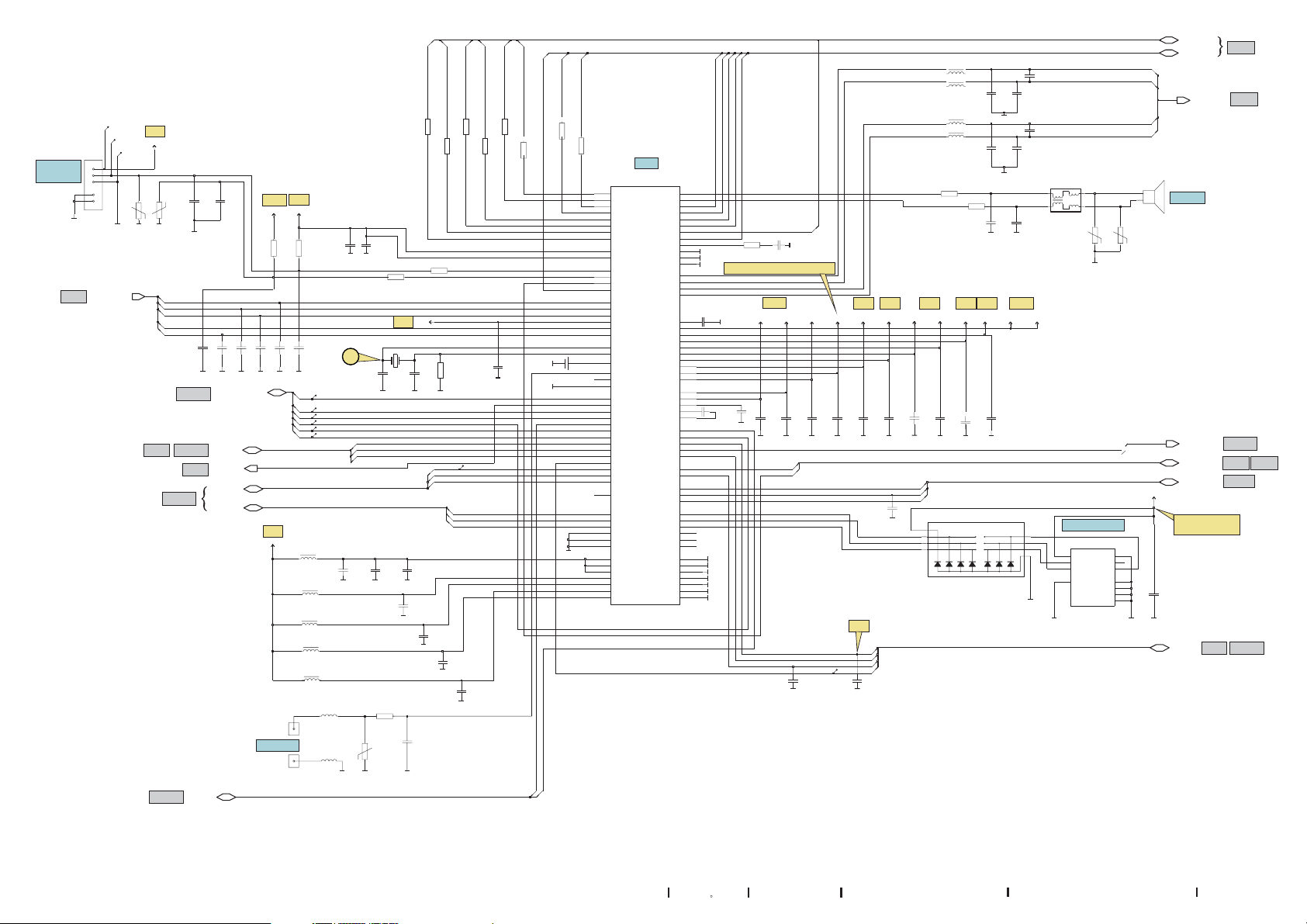
RAPGSM, memory & micro SD card
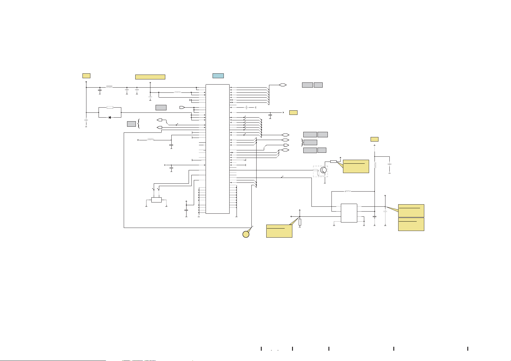
RET
U
TAHVO
Front UI, display & B2B connectors
FM radio & Bluetooth
RF-part
Signal overview
Component finder
Exploded view and component disposal
1
2
3
4
5
6
7
8
9
Copyright © NOKIA
This material, including documentation and any related computer programs is protected
by copyright, controlled by NOKIA. All rights are reserved. Copying, including reproducing,
modifying, storing, adapting or translating any or all of this material requires the prior
written consent of NOKIA. This material also contains confidential information, which may
not be disclosed to others without the prior written consent of NOKIA.
Customer Care / Service & Support Readiness / Content Creation Management
Copyright © 2005 NOKIA Only for training and service purposes
Version: 1.0 11.
11.2005 3250 RM-38
Board version: 1hx_13a
Front page
Page 1(9)

Battery
connector
GND
TAHVO
X2070
VBATT
BSI
GND
GND
J2070
BGND
SLOWAD(6:0)
J2071
J2072
71
R20
3,7V
VBAT
14V/50V
GNDGND
TAHVO
RAPGSM
BSI
BTEMP
R2070
47k
5
6
1
4
0
RAPGSM
GND
LS
LST
RFTEMP
VCHAR
WTXDET
C2202
1n0
RAPGSM
RAPGSM
TAHVO
ACI(1:0)
C2071
GND
27p
C2203
1n0
INT_SIM(5:0)
C2072
C2204
GND
DIG_AUDIO(5:0)
CBUS(3:0)
CHSWSTAT
TXC(2:0)
0
1
2
3
VSIM1
B2100
GND
C2700
100n
AUDIO(8:0)
XAUDIO(7:0)
H_BRIDGE(3:0)
Earpiece
EMINT(1:0)
USB_ACI(7:0)
TXC_CONV(2:0)
1.8V/3V depends
on SIM card
PUSL(7:0)
TAHVO
X2400
X1000
RAPGSM
TAHVO X2400
RF-Part
RAPGSM
8
67
R2204
R2202
1k0
1k0
R2203
1k0
2.5V
1.35V
27p
C2205
1n0
VREF_INT
R2200
100k
C2206
1n0
GND
3,7V
Power key
VANA
R2201
120k
C2207
1n0
1n0
GNDGND
GND
0
J2200
J2201
1
2
J2202
J2203
3
4
J2204
5
J2205
VBAT
L2202
220R/100MHz
L2204
600R/100MHz
L2203
600R/100MHz
L2205
22 0R /10 0M Hz
L2206
60 0R/1 00 MH z
L2411
X2403
X2404
15nH
L2410
15nH
C2223
C2224
10n
10n
GND
GND
32.768kHz
1
0
1
2
C2226
C2225
1u0 1u0
1u0
GND
GND
R2408
4k7
14V/ 50V
R2409
GND
GND
R2214
B2200
C2208
C2408
27p
R2213
4k7
4k7
VBAT
3,7V
R2216
2M2
C2209
22p
27p
GNDGND
GND
J2210
0
2
1
0
2
1
C2227
GND
C2230
1u0
GND
C2228
1u0
GND
C2231
10U
GND
C2232
1u0
GND
GND
1k0
R2205
34
0
R2207
1k0
R2208
1k0
R2209
1k0
RETU
D2200
RETU_3.02
K1
Mic1P
J3
Mic1N
J1
Mic2P
J2
Mic2N
E1
Mic3P
E2
Mic3N
E3
Mic3PR
D2
Mic3NR
C3
VDARx
K2
VDATx
M12
BSI
L3
BTemp
L11
HeadDet
L12
HookDet
M2
LS
L2
LST
M1
RFTemp
G10
VBat6
F10
VChar VRef
M3
WTxDet
L9
CrI
K9
CrO
G2200
L8
GND
GND
VBack
E12
PwrOnX
L1
SIMDetX
J11
WDDis
M4
AudClk
K10
ChSwS
A4
EarDaL
B4
EarDaR
L4
MBusTx
A3
PMARP
C4
PMARN
M5
SerClk
L5
SerData
K5
SerSelX
J10
SleepX
M6
TxCClk
L7
TxCCtrl
L6
TxCDa
M10
HV
C5
SIMClk1
C6
SIMDa1
A5
SIMIOC1
B6
SIMClk2
A6
SIMDa2
B7
SIMIOC2
GND
C12
VBat1
K11
VBat2
A8
VBat3
H12
VBat4
F12
VBat5
B12
VBatCP
B3
XEarL
XEarLC
XEarR
XEarRC
MicB1
MicB2
MicBCap
VSARx
VSATx
MicSub
HFSpP
HFSpN
VibraP
VibraN
VDRAM
VRFC
VSIM1
VSIM2
VRCP1
VRCP2
FlyHigh
FlyLow
MBusRx
MicData
PURX
RetuInt
SIMClkC1
SIMDaC1
SIMRstC1
SIMClkC2
SIMDaC2
SIMRstC2
GndCP
GndHVBatH
D3
EarP
D1
EarN
F3
F1
G1
G3
H1
H2
G2
C1
H3
F2
B1
C2
A2
A1
H10
VBG
F11
J12
VAna
E11
VAux
M11
D12
VIO
G11
VR1
G12
A7
C9
A10
C10
B10
VCP
B11
A12
K4
B5
K3
K8
M9
SlClk
H11
MBus
E10
RstX
M8
AFC
K7
TxC1
M7
TxC2
C7
C8
C11
B9
A9
D10
L10
TM
D11
Gnd1
K12
Gnd2
B8
Gnd3
K6
Gnd4
A11
B2
R2206
1k0
C2281
1u0
GND
132
4567
R2212
470R
GND
GND
GND
1.8V/3V depends on SIM card
C2201
1u0
GND
1u0
C2210
C2211
4u7
1u0
GND
GND
GND
GND
GND
GND
GND
GND
GND
4.75V
{
C2221
C2200
1u0
VRCP1VRCP2
C2222
1u0
GND
3
7
2
GND
VSIM2 VRFC
C2220
1u5
1u5
GND GND
1.8V
S
2.5V
C2212
VR1 FERVUV1
C2213
C2214
1u5
1u5
GND
GND
C2233
27p
GND
I
1.8V
0
1
2
J2219
3
C2218
1n0
GND
PWRONX
C2229
1n0
GND
051
L2270
HFSPP
220R/100MHz C2270 1n0
HFSPN
L2271
22 0R/ 100 M Hz
L2272
VIBRAP
220R/100MHz
VIBRAN
L2273
220R/100MHz
R2102
10R
1.8V{2.8V 2.5V
C2219
C2215
1u5
1u5
1u5
GND
GND
0
1
2
EMIF03-SIM02F2
CLK
R2103
10R
XMV
A
C2216
GND
R2700
C2271
C2272
1n0
GND
C2274 C2275
GND
C2103
1n 0 1 n0
GND
N
AVOIV
VREF_INTVDRAM
A
C2217
1u5
GND
SIM Reader
R1
R2
R3
1n0
1n01n0
C2273
{
GND
1n0
GND
1.35V
Side
CLK
C2104
L2100
EXC24CB102U
2
14
SIM card reader
2
1
7
GND
GND
3
21 04
R
GND
X2700
SF7W006S4C
C13C5
C2
C3
SW8GND
/50V
14 V
14 V/50 V
R2105
0
4
5
C6
6
C7
9
GND
10
GND
11
GND
GND
Customer Care / Service & Support Readiness / Content Creation Management
Copyright © 2005 NOKIA Only for training and service purposes
Version: 1.0 11.11.
2005 3250 RM-38
Board version: 1hx_13a
RETU
Page 2(9)

C2306
3,7V
VBAT
1u0
GND
C2309
22u
GND
RSX101VA-30TR
L2301
220R/100MHz
R2307
100R
V2302
C2300
10n
GND
1.35V in local mode
C2301
22u
GND
C2302
SLOWAD(6:0)
RETU
CHSWSTAT
VBAT
VCORE
22u
GND
L2306
VBAT_N2300-G9
600R/100MHz
23
1
CURRENT_SEN_30um
R2300
GND
X2400
VOUT
J2306J2307
L2 30 2
10uH
GND
CHARGER
4
J2300
GND
GND
C2307
1u0
GND
GND
C2312
1u0
GND
SENSE+
SENSE-
4
BGND
VBUS
GND
C2313
1u0
TAHVO
N230 0
TAHVO_V5.2_LF
A7
VBAT1
A6
VBAT1
A5
VCoreCoil
B6
VCoreCoil
B4
VCore
B5
GND1
A4
GND1
D10
VCharIn1
E10
VCharIn2
E9
VCharInK
F10
VCharOut1
G10
VCharOut2
F9
VCharOutK
D9
VCharADC
J1
ChSwS
F1
SMPSClk
F2
GND4
G9
VBAT3
J8
GND3
A10
NC
B10
NC
A8
NC
C10
NC
B8
NC
A9
GND5
H10
Vout
G2
SENSE+
H2
SENSE-
K10
VCC
H3
NC
H4
NC
H5
NC
H6
NC
H7
NC
H8
NC
G3
NC
G8
NC
F3
NC
F8
NC
NG
Slave_PU
Master_PD1
Master_PD2
D+_RXD
D-_TXD
VPP_VIO
VCCint
RCV_FRX2
VP_FRX
VM_CLK
SLAVESWSET
PURX
SLEEPX
TahvoInt
CbusData
CbusSelX
CbusClk
VcoreDef
FlashM
TestMode
TestOut
GenOut1
GenOut2
GenOut3
PWM300
Clk600
SleepClk
RXD2
FSE0
RSTX
J10
H9
J9
J6
CLK
K7
J7
K8
A1
C2303 1u0
K9
A3
VIO
OEX
VO
FTX
NC
NC
NC
NC
NC
NC
NC
NC
NC
NC
J2309
J4
J2314
K4
J2310
J5
K2
J2311
J2312
J3
K3
J2313
K5
J2315
K6
B3
D2
D1
C2
C1
B1
B2
C9
A2
B7
B9
J2
K1
H1
G1
E1
E2
E3
E8
D3
D8
C3
C4
C5
C6
C7
C8
DNGD
2
4
5
6
3
2
1
0
GND
5
4
GND
3
2
1
0
6
7
2
0
3
1
GND
GND
7
1
5
J2308
Display LEDs
on: 0.5V
off: 0V
C2304
10n
1
2
0
SETCURR1
VIO
J2316
USB_ACI(7:0)
1.8V
INTUSB(8:0)
PUSL(7:0)
EMINT(1:0)
CBUS(3:0)
SETCURR2
X2400 RETU
RAPGSM
RAPGSM
RAPGSM
0
4
2
R
3
7
R
2
GND
TAHVO
V2300
DTC143ZM-T2L
R1
IN
4k7
R2
PWMTAHVO
RETU
47k
3,7V
VBAT
SETCURR3
R2305
Keyboard LEDs
1k2
OUT
on: 10V
off: 0V
GND
GND
4W_LED_DRIVER
A2
EN
C2
IND
B3
FB
A3
NC
L2304
22 uH
N2301
C1
VOUT
B1
VDD
A1
AGND
C3
PGND
GN D
C2314
C2305
L2305
1u0
600R/100MHz
GND
VBAT_N2301-B1
VLEDOUT1
Keyboard LEDs
C2315
4u7
4u7
GND
on: 15V
off: 0V
Display LEDs
on: 15V
GND
off: 0V
Customer Care / Service & Support Readiness / Content Creation Management
Copyright © 2005 NOKIA Only for training and service purposes
Version: 1.0 11.
11.2005 3250 RM-38
Board version: 1hx_13a
TAHVO
Page 3(9)
 Loading...