

Page 1

CC Technical Documentation
RM-11 Series Transceivers
Troubleshooting - Baseband
Issue 1 02/2004 Confidential ©2004 Nokia Corporation
Page 2

RM-11
Troubleshooting - Baseband CC Technical Documentation
Contents Page
Troubleshooting Overview ............................................................................................ 4
Power Up and Reset .....................................................................................................6
Power Up - Power Key.............................................................................................. 8
Power Up - Charger................................................................................................... 8
Power Up - RTC Alarm ............................................................................................ 9
Power Off .....................................................................................................................9
Power Consumption and Operation Modes .................................................................9
Power .........................................................................................................................10
Clock Distribution .....................................................................................................11
RFClk (19.2 MHz Analog)...................................................................................... 11
RFConvClk (19.2 MHz Digital).............................................................................. 12
CBUSClk Interface ................................................................................................. 13
DBUS Clk Interface ................................................................................................ 13
SleepCLK (Digital)................................................................................................. 14
SleepCLK (Analog)................................................................................................. 15
Flash Programming ....................................................................................................15
Connections to Baseband........................................................................................ 15
Baseband Power Up ................................................................................................ 15
Flash Programming Indication................................................................................ 15
Flashing................................................................................................................... 16
Flash Programming Error Codes............................................................................. 18
Charging Operation ...................................................................................................19
Battery..................................................................................................................... 19
Charging Circuitry................................................................................................... 20
Charger Detection ......................................................................................................21
Charge Control........................................................................................................ 22
Audio .........................................................................................................................22
Display and Keyboard ...............................................................................................23
Flashlight................................................................................................................. 23
Camera .......................................................................................................................24
DC Measurements................................................................................................... 25
AC Measurements................................................................................................... 26
Timing Measurements............................................................................................. 26
Power-up Timing..................................................................................................... 27
UIF Interface Timing Measurements...................................................................... 28
FM Radio ...................................................................................................................30
FM Radio Test......................................................................................................... 31
Accessories ................................................................................................................33
Charging.................................................................................................................. 33
Tomahawk Headset Detection ................................................................................ 34
FBus Detection........................................................................................................ 35
Accessory Detection Though ACI .......................................................................... 36
RUIM (SIM CAR) .....................................................................................................37
Test Points .................................................................................................................39
Camera Test Points.................................................................................................. 41
Top Troubleshooting Map .........................................................................................42
Phone is Totally Dead ................................................................................................44
Page 2 ©2004 Nokia Corporation Confidential Issue 1 02/2004
Page 3

RM-11
CC Technical Documentation Troubleshooting - Baseband
Flash Programming Does Not Work .........................................................................45
Phone is Jammed .......................................................................................................47
Power Does Not Stay on or the Phone is Jammed .....................................................48
Charger Faults ............................................................................................................49
Audio Faults ...............................................................................................................50
Earpiece................................................................................................................... 50
Microphone ............................................................................................................. 51
Vibra........................................................................................................................ 52
Display Faults ............................................................................................................53
Keypad Faults ............................................................................................................55
Power Key............................................................................................................... 55
UI Modules.............................................................................................................. 56
FM Radio................................................................................................................. 57
Camera .................................................................................................................... 59
Flashlight................................................................................................................. 60
GPS Module ...............................................................................................................60
Overview................................................................................................................. 60
Issue 1 02/2004 ©2004 Nokia Corporation Confidential Page 3
Page 4

RM-11
Troubleshooting - Baseband CC Technical Documentation
Troubleshooting Overview
The baseband module of the RM-11 transceiver is a trimode, CDMA, dual-band engine
and consists of three main Application Specific Integrated Circuits (ASICs):
• Universal Energy Management (UEM)
• Universal Phone Processor (UPP)
• A 128-Megabit FLASH
The baseband architecture is based on the DCT4 Apollo engine and supports a
power-saving function called sleep mode. Sleep mode shuts off the VCTCXO, which is
used as a system clock source for both the RF and the baseband. The phone awakens by a
timer running from this 32 kHz clock. The sleep time is determined by network
parameters. During the sleep mode, the system runs from a 32 kHz crystal. Sleep mode is
entered when both the MCU and the DSP are in standby mode, and the 19.2 MHz Clk
(VCTCXO) is switched off.
The RM-11 supports both two and three DCT3 type wire chargers. However, the 3-wire
chargers are treated as two-type wire chargers. Charging is controlled by the UEM ASIC
and EM SW.
A BLD-3 Li-ion battery is used as the main power source. The BLD-3 has a nominal
capacity of 780 mAh.
Page 4 ©2004 Nokia Corporation Confidential Issue 1 02/2004
Page 5
RM-11
CC Technical Documentation Troubleshooting - Baseband
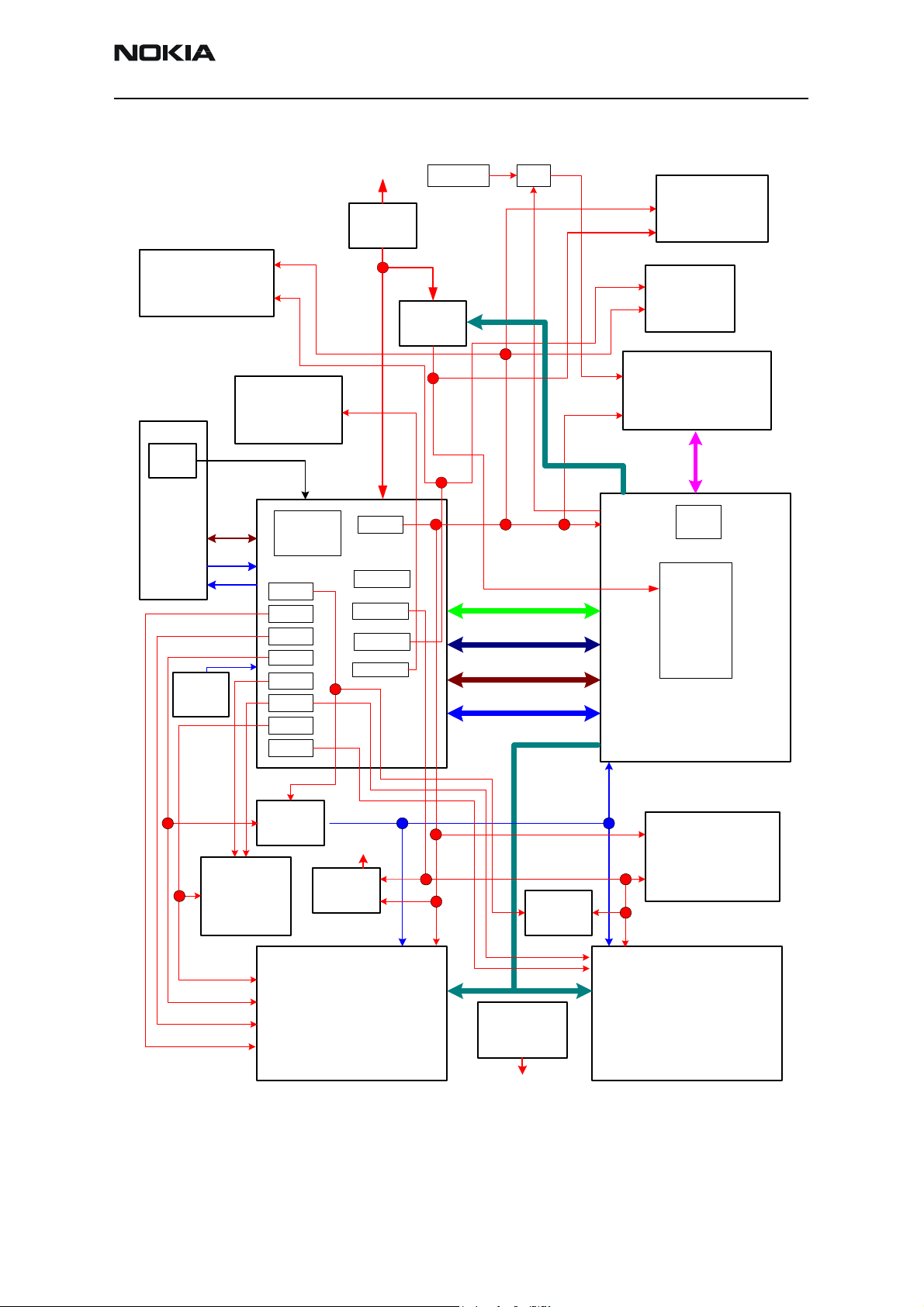
FM Radio
Charger
Bottom
Conn.
Sleep Clk
32 KHz
SIM Reader
MBus
FBusRx
FBusT
x
UEM
VR1A
VR1B
VR2
VR3
VR4
VR5
VR6
VR7
VBatt
Battery
VIO
VANA
Vflash1
Vflash2
VSIM
DC/DC
VPPPRODTP
GenIO
Control
CBus
DBus
MBus
FBus
GPS
BB_RF
Camera
Flash
ExtBusC
UPP
Core
VCTCXO
19.2 MHz
Front
End
VBatt
IR
RF
Bus
UHF
SYNTH
LCD/Key
Flashlight
Robin Batman
PA
VBatt
Figure 1: RM-11 power distribution
Issue 1 02/2004 ©2004 Nokia Corporation Confidential Page 5
Page 6

RM-11
Troubleshooting - Baseband CC Technical Documentation
Power Up and Reset
Power up and reset are controlled by the UEM ASIC. The RM-11 baseband can be
powered up in the following ways:
• By the Power button, which means grounding the PWRONX pin of the UEM
• By connecting the charger to the charger input
• By the RTC alarm, when the RTC logic has been programmed to give an alarm
After receiving one of the above signals, the UEM counts a 20ms delay and enters into
reset mode. The watchdog starts up, and if the battery voltage is greater than Vcoff+,
a 200ms delay starts to allow references (etc.) to settle. After this delay elapses, the
VFLASH1 regulator is enabled. Then, 500us later the VR3, VANA, VIO, and VCORE are
enabled. Finally, the power-up reset (PURX) line is held low for 20 ms. The PURX reset is
fed to the baseband UPP ASIC. Resets are generated for the MCU and the DSP. During
this reset phase, the UEM forces the VCTCXO regulator on — regardless of the status of
the sleep control input signal — to the UEM. The FLSRSTx from the ASIC is used to reset
the flash during power up and to put the flash in power down during sleep. All baseband
regulators are switched on when the UEM powers on. The UEM internal watchdogs are
running during the UEM reset state, with the longest watchdog time selected. If the
watchdog expires, the UEM returns to the power-off state. The UEM watchdogs are
internally acknowledged at the rising edge of the PURX signal in order to always give the
same watchdog response time to the MCU.
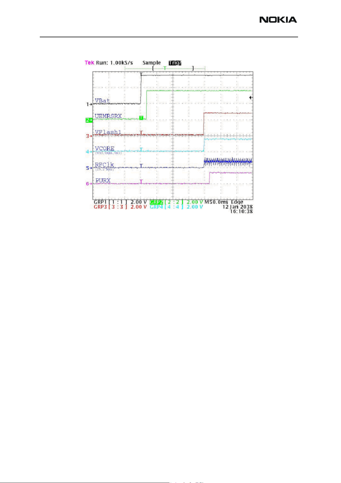
Figure 2 represents the UEM start-up sequence from reset to power-on modes.
Page 6 ©2004 Nokia Corporation Confidential Issue 1 02/2004
Page 7

RM-11
CC Technical Documentation Troubleshooting - Baseband
Reference signal
PwrOnX
Charger Detection
RTC
UEMRSTX
VFlash1
VIO
VCORE
VANA
VR3
19.2MHz Clk
PURX
32kHz XTAL
Figure 2: UEM start-up sequence from reset to power-on mode
t1 t2 t4t3
t1 = 20ms
t2 = 200ms
t3 = 500us
t4 = 20ms
Issue 1 02/2004 ©2004 Nokia Corporation Confidential Page 7
Page 8
RM-11
Troubleshooting - Baseband CC Technical Documentation
Power Up - Power Key
When the Power key is pressed, the UEM enters the power up sequence. Pressing the
Power key causes the PWRONX pin on the UEM to be grounded. The UEM PWRONX
signal is not part of the keypad matrix. The Power key is only connected to the UEM. This
means that when pressing the power key, an interrupt is generated to the UPP that starts
the MCU. The MCU then reads the UEM interrupt register and notices that it is a
PWRONX interrupt. Then the MCU reads the status of the PWRONX signal using the UEM
control bus (CBUS). If the PWRONX signal stays low for a specific duration, the MCU
accepts this as a valid power on state and continues with the SW initialization of the
baseband. If the power on key does not indicate a valid power on situation, the MCU
powers off the baseband.
Power Up - Charger
In order to be able to detect and start charging in the case where the main battery is
fully discharged (empty) and hence the UEM has no supply (NO_SUPPLY or BACKUP
mode of UEM), charging is controlled by START-UP CHARGING circuitry.
Whenever a VBAT level is detected to be below the master reset threshold (VMSTR-),
charging starts and is controlled by START_UP charge circuitry. Connecting a charger
forces the VCHAR input to rise above the charger detection threshold (VCHDET+) and by
detection charging is started. The UEM generates 100 mA constant output current from
the connected charger's output voltage. The battery’s voltage rises as it charges, and
when the VBAT voltage level is detected to be higher than the master reset threshold
limit (VMSTR+), the START_UP charge is terminated.
Figure 3: Power up
Page 8 ©2004 Nokia Corporation Confidential Issue 1 02/2004
Page 9

RM-11
CC Technical Documentation Troubleshooting - Baseband
Monitoring the VBAT voltage level is done by the charge control block (CHACON). A
MSTRX='1' output reset signal (internal to the UEM) is given to the UEM's RESET block
when the VBAT>VMSTR+ and UEM enter into the reset sequence.
If VBAT is detected to fall below VMSTR- during start-up charging, charging is cancelled.
It will restart if new rising edge on the VCHAR input is detected (VCHAR rising above
VCH-ET+).
Power Up - RTC Alarm
If phone is in POWER_OFF mode when an RTC alarm occurs, a wake-up procedure begins.
After the baseband is powered ON, an interrupt is given to the MCU. When an RTC alarm
occurs during ACTIVE mode, an interrupt is generated to the MCU.
Power Off
The baseband switches into power off mode if any of following occurs:
• Power key is pressed
• Battery voltage is too low (VBATT < 3.2 V)
• Watchdog timer register expires
The UEM controls the power down procedure.
Power Consumption and Operation Modes
During power off mode, power (VBAT) is supplied to the UEM, BUZZER, VIBRA, LED, PA,
and PA drivers (Tomcat and Hornet). During this mode, the current consumption is
approximately 35 uA, which is the UEM leakage current.
In sleep mode, both processors (MCU and DSP) are in stand-by mode. The phone enters
sleep mode only when both processors make this request. When the SLEEPX signal is
detected low by the UEM, the phone enters SLEEP mode. The VIO and VFLASH1
regulators are put into low quiescent current mode, VCORE enters LDO mode, and the
VANA and VFLASH2 regulators are disabled. All RF regulators are disabled during SLEEP
mode. When the UEM detects a high SLEEPX signal, the phone enters ACTIVE mode and
all functions are activated.
The sleep mode is exited either by the expiration of a sleep clock counter in the UEM or
by some external interrupt (a charger connection, key press, headset connection, etc.).
In sleep mode, the VCTCXO (19.2 MHz Clk) is shut down and the 32 kHz sleep clock
oscillator is used as a reference clock for the baseband.
The average current consumption of the phone can vary depending mainly on the SW
state (e.g., slot cycle 0, 1, or 2) and if the phone is working on IS95 or IS2000 for CDMA.
However, the average consumption is about 6 mA in slot cycle 0 on IS95.
Issue 1 02/2004 ©2004 Nokia Corporation Confidential Page 9
Page 10

RM-11
Troubleshooting - Baseband CC Technical Documentation
In the ACTIVE mode, the phone is in normal operation; scanning for channels, listening to
a base station, and transmitting and processing information. There are several sub-states
in the active mode depending on the phone’s present state, such as burst reception, burst
transmission, if DSP is working, etc.
In active mode, SW controls the UEM RF regulators: VR1A and VR1B can be enabled or
disabled. These regulators work of the UEM charge pump. VSIM can be enabled or
disabled and its output voltage can be programmed to be 1.8 V or 3.3 V. VR2 and
VR4–VR7 can be enabled, disabled, or forced into low quiescent current mode. VR3 is
always enabled in active mode and disabled during sleep mode and cannot be controlled
by SW in the same way as the other regulators. VR3 will only turn off if both processors
(DSP and MCU) request to be in sleep mode.
CHARGING mode can be performed in parallel with any other operating mode. A BSI
resistor inside the battery indicates the battery type/size. The resistor value corresponds
to a specific battery type and capacity. This capacity value is related to the battery
technology.
Power
The battery voltage, temperature, size and charging current are measured by the UEM,
and the EM charging algorithm controls it.
The charging control circuitry (CHACON) inside the UEM controls the charging current
delivered from the charger to the battery. The battery voltage rise is limited by turning
the UEM switch off when the battery voltage reaches 4.2 V. The charging current is
monitored by measuring the voltage drop across a 220 mOhm resistor.
In normal operation, the baseband is powered from the phone's battery. The battery
consists of one Lithium-Ion cell. In the case of RM-11, the battery capacity is 780 mAh.
The UEM ASIC controls the power distribution to the whole phone through the BB and RF
regulators excluding the power amplifier (PA) and the DC/DC, which have a continuous
power rail directly from the battery. The battery feeds power directly to the following
parts of the system:
•UEM
•PA
•DC/DC
• Buzzer
•Vibra
• Display and keyboard lights
The UEM is the heart of the power distribution to the phone, which includes all the
voltage regulators. The UEM handles power-up hardware functions so the regulators are
not powered and the power-up reset (PURX) is not released if the battery voltage is less
than 2.8 V.
Page 10 ©2004 Nokia Corporation Confidential Issue 1 02/2004
Page 11
RM-11
CC Technical Documentation Troubleshooting - Baseband
The RM-11 baseband is powered from five different UEM regulators:
Table 1: RM-11 Baseband Regulators
Regulator
VCORE
DD/DC
VIO 150 1.8 Enabled always except during power-off mode
VFLASH1 70 2.78 Enabled always except during power-off mode
VFLASH2 40 2.78 Enabled only when data cable is connected
VANA 80 2.78 Enabled only when the system is awake (off during sleep
VSIM 25 3.0 Not used
Maximum
current (mA)
300 1.5 Output voltage selectable 1.0V/1.3V/1.5V/1.8V
Vout (V) Notes
Default power at power-up is 1.5V
and power-off modes)
Table 2 includes the UEM voltage regulators used by the RF.
Table 2: RM-11 RF Regulators
Regulator
VR1A 10 4.75 Enabled when the receiver is on
Maximum
current (mA)
Vout (V) Notes
VR1B 10 4.75 Enabled when the transmitter is on
VR2 100 2.78 Enabled when the transmitter is on
VR3 20 2.78 Enabled when SleepX is high
VR4 50 2.78 Enabled when the receiver is on
VR5 50 2.78 Enabled when the receiver is on
VR6 50 2.78 Enabled when the transmitter is on
VR7 45 2.78 Enabled when the receiver is on
A charge pump used by VR1A is constructed around the UEM. The charge pump works
with Cbus (1.2 MHz Clk) and gives a 4.75 V regulated output voltage to the RF.
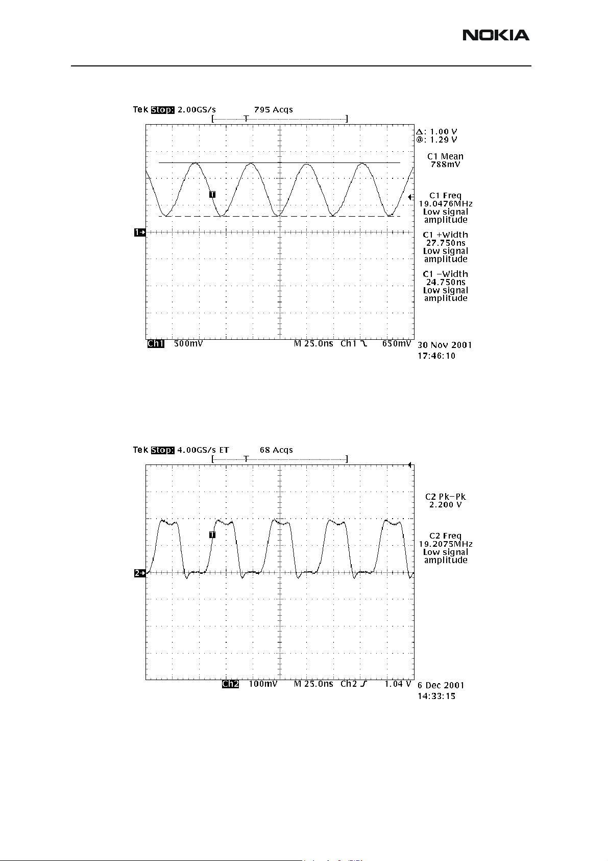
Clock Distribution
RFClk (19.2 MHz Analog)
The baseband’s main clock signal is generated from the VCTCXO (G503). This 19.2 MHz
clock signal is generated at the RF and fed to the UPP’s RFCLK pin.
Issue 1 02/2004 ©2004 Nokia Corporation Confidential Page 11
Page 12
RM-11
Troubleshooting - Baseband CC Technical Documentation
RFConvClk (19.2 MHz Digital)
The UPP distributes the 19.2 MHz Clk to the internal processors, DSP, and MCU, where
SW multiplies this clock by seven for the DSP and by two for the MCU.
Figure 4: 19.2 MHz analog
Figure 5: 19.2 MHz digital
Page 12 ©2004 Nokia Corporation Confidential Issue 1 02/2004
Page 13
RM-11
CC Technical Documentation Troubleshooting - Baseband
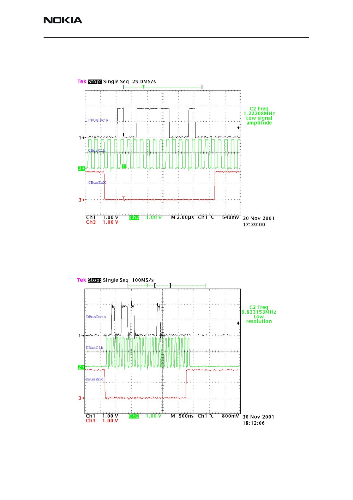
CBUSClk Interface
A 1.2 MHz clock signal is used for CBUS, which is used by the MCU to transfer data
between the UEM and UPP.
DBUS Clk Interface
A 9.6 MHz clock signal is used for DBUS, which is used by the DSP to transfer data
between the UEM and the UPP.
Figure 6: 1.2 MHz CBUS clock signal
Figure 7: 9.6 MHz clock signal
Issue 1 02/2004 ©2004 Nokia Corporation Confidential Page 13
Page 14
RM-11
Troubleshooting - Baseband CC Technical Documentation
The system clock can be stopped during sleep mode by disabling the VCTCXO power
supply from the UEM regulator output (VR3) by turning off the controlled output signal
SLEEPX from the UPP.
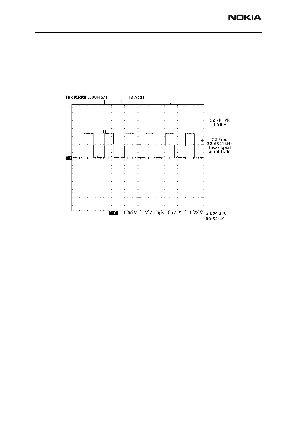
SleepCLK (Digital)
The UEM provides a 32 kHz sleep clock for internal use and to the UPP, where it is used
for the sleep mode timing.
Figure 8: 32 kHz digital sleep clock signal
Page 14 ©2004 Nokia Corporation Confidential Issue 1 02/2004
Page 15
RM-11
CC Technical Documentation Troubleshooting - Baseband
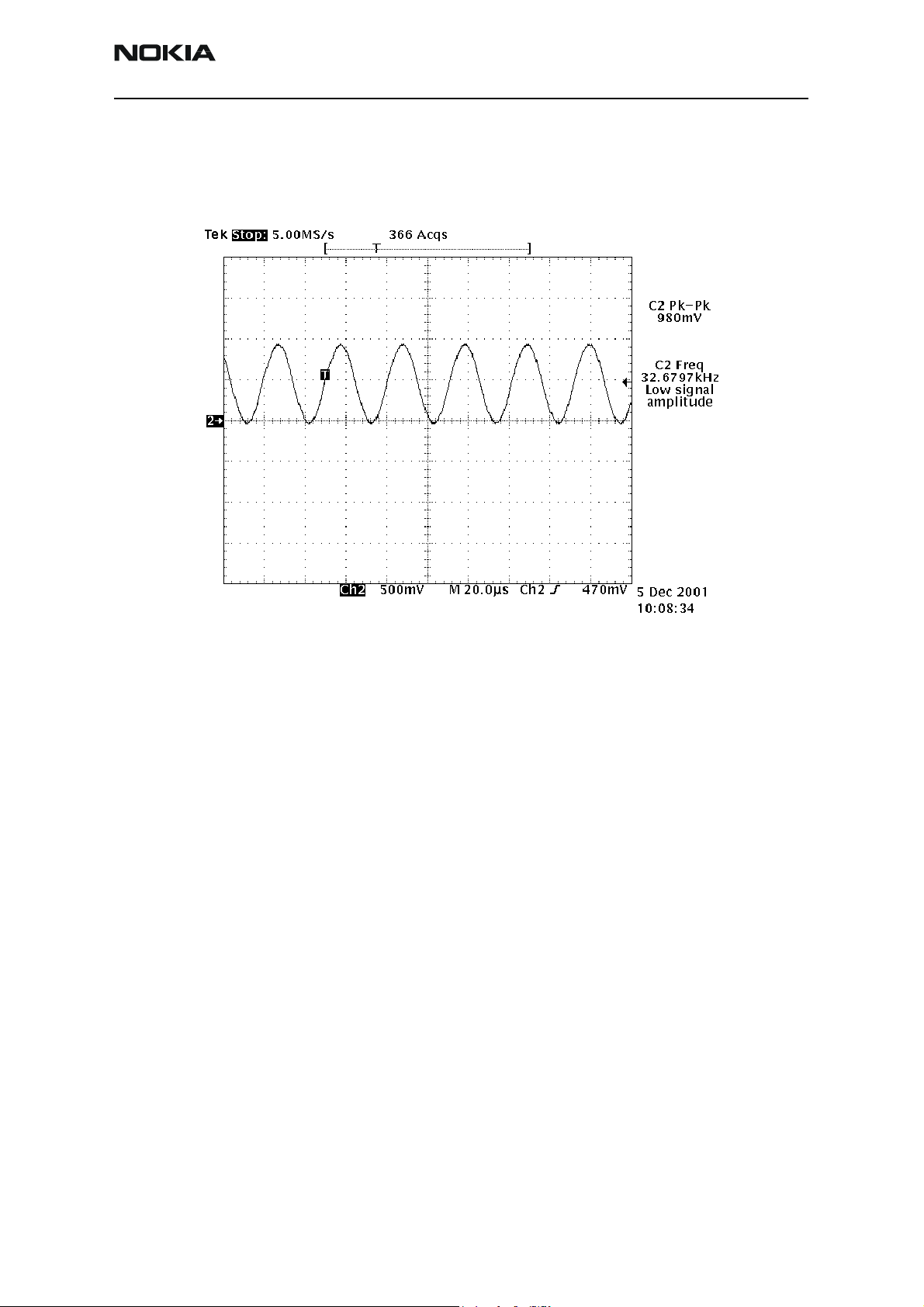
SleepCLK (Analog)
When the system enters sleep mode or power off mode, the external 32 KHz crystal
provides a reference to the UEM RTC circuit to turn on the phone during power off or
sleep mode.
Figure 9: 32 KHz analog sleep clock signal
Flash Programming
Connections to Baseband
The flash programming equipment is connected to the baseband using test pads for
galvanic connection. The test pads are allocated in such a way that they can be accessed
when the phone is assembled. The flash programming interface consists of the VPP,
FBUSTX, FBUSRX, MBUS, and BSI signals and is used by the FPS-8 to flash. The
connection is through the UEM, which means that the logic voltage levels correspond to
2.78 V. Power is supplied to the phone using the battery contacts.
Baseband Power Up
The baseband power is controlled by the flash prommer in production and in
re-programming situations. Applying supply voltage to the battery terminals causes the
baseband to power up. Once the baseband is powered, flash programming indication
begins (see the following "Flash Programming Indication" section).
Flash Programming Indication
Flash programming is indicated to the UPP using the MBUSRX signal between the UPP
and UEM. The MBUS signal from the baseband to the flash prommer is used as a clock
for the synchronous communication. The flash prommer keeps the MBUS line low during
UPP boot to indicate that the flash prommer is connected. If the UPP MBUSRX signal is
low on the UPP, the MCU enters flash-programming mode. In order to avoid accidental
entry to the flash-programming mode, the MCU only waits for a specified time to get
Issue 1 02/2004 ©2004 Nokia Corporation Confidential Page 15
Page 16

RM-11
Troubleshooting - Baseband CC Technical Documentation
input data from the flash prommer. If the timer expires without any data being received,
the MCU continues the boot sequence. The MBUS signal from the UEM to the external
connection is used as a clock during flash programming. This means that the
flash-programming clock is supplied to the UPP on the MBUSRX signal.
The flash prommer indicates flash programming/reprogramming to the UEM by writing
an 8-bit password to the UEM. The data is transmitted on the FBUSRX line and the UEM
clocks the data on the FBUSRX line into a shift register. When the 8 bits have been
shifted in the register, the flash prommer generates a falling edge on the BSI line. This
loads the shift register content in the UEM into a compare register. Programming starts if
the 8-bits in the compare register match with the default value preset in the UEM. At
this point the flash prommer pulls the MBUS signal to UEM low in order to indicate to
the MCU that the flash prommer is connected. The UEM reset state machine performs a
reset to the system, PURX low for 20 ms. The UEM flash programming mode is valid until
the MCU sets a bit in the UEM register that indicates the end of flash programming.
Setting this bit also clears the compare register in the UEM, which was loaded at the
falling edge of the BSI signal. The UEM watchdogs are disabled during the flash
programming mode. Setting the bit indicating the end of flash programming enables and
resets the UEM watchdog timer to its default value. Clearing the flash programming bit
also causes the UEM to generate a reset to the UPP.
Flashing
The BSI signal is used to load the value into the compare register. In order to avoid
spurious loading of the register, the BSI signal is gated during the UEM master reset and
during power on when PURX is active. The BSI signal should not change states during
normal operation unless the battery is extracted. In this case the BSI signal will be pulled
high. Note that a falling edge is required to load the compare register.
Flash programming is done through the VPP, FBUSTX, FBUSRX, MBUS, and BSI signals.
When the phone enters flash programming mode, the prommer indicates to the UEM
that flash programming will take place by writing an 8-bit password to the UEM. A
prommer first sets the BSI to "1", uses FBUSRX for writing, and uses the MBUS for
clocking. The BSI is then set back to "0".
The MCU uses the FBUSTX signal to indicate to the prommer that it has been noticed.
Then the MCU reports the UPP type ID and is ready to receive the secondary boot code in
its internal SRAM.
Page 16 ©2004 Nokia Corporation Confidential Issue 1 02/2004
Page 17
RM-11
CC Technical Documentation Troubleshooting - Baseband
FLASH_1
CH1 = BSI
CH2 = MBUS
CH3 = FBUSTX
CH4 = FBUSRX
Measure points
Production test pattern
(J396)
Figure 10: Flashing start
This boot code asks the MCU to report the prommer phone’s configuration information,
including the flash device type. Now the prommer can select and send the algorithm
code to the MCU SRAM (and SRAM/Flash self-tests can be executed).
FLASH_2
CH1 = PURX
CH2 = MBUS
CH3 = FBUSTX
CH4 = FBUSRX
Measure points
Production test pattern
(J396)
Figure 11: Flashing, continued 1
• Ch1-> PURX
• Ch2-> MBUS toggled three times for MCU initialization
• Ch3-> FBUS_TX low, MCU indicates that prommer has been noticed
• Ch4-> FBUS_RX
Issue 1 02/2004 ©2004 Nokia Corporation Confidential Page 17
Page 18
RM-11
Troubleshooting - Baseband CC Technical Documentation
FLASH_3
CH1 = PURX
CH2 = MBUS
CH3 = FBUSTX
CH4 = FBUSRX
Measure points
Produ c tio n te s t pattern
(J396)
Data transfer has
started (Fbus_Rx)
Figure 12: Flashing, continued 2
Flash Programming Error Codes
The following characteristics apply to the information in Table 3.
• Error codes can be seen from the test results or from Phoenix's flash-tool.
• Underlined information means that the connection under consideration is being
used for the first time.
Table 3: Flash programming error codes
Error Description Not Working Properly
C101 "The Phone does not set FbusTx line high after
the startup."
C102 "The Phone does not set FbusTx line low after
the line has been high. The Prommer generates
this error also when the Phone is not connected to the Prommer."
C103 " Boot serial line fail." Mbus from Prommer->UEM->UPP(MbusRx)(SA1)
Vflash1
VBatt
BSI and FbusRX from prommer to UEM.
FbusTx from UPP->UEM->Prommer(SA0)
PURX(also to Safari)
VR3
Rfclock(VCTCXO->Safari->UPP)
Mbus from Prommer->UEM->UPP(MbusRx)(SA0)
FbusTx from UPP->UEM->Prommer(SA1)
BSI and FbusRX from prommer to UEM.
FbusRx from Prommer->UEM->UPP
FbusTx from UPP->UEM->Prommer
C104 "MCU ID message sending failed in the Phone." FbusTx from UPP->UEM->Prommer
C105 "The Phone has not received Secondary boot
codes length bytes correctly."
Mbus from Prommer->UEM->UPP(MbusRx)
FbusRx from Prommer->UEM->UPP
FbusTx from UPP->UEM->Prommer
Page 18 ©2004 Nokia Corporation Confidential Issue 1 02/2004
Page 19
RM-11
CC Technical Documentation Troubleshooting - Baseband
Table 3: Flash programming error codes (Continued)
Error Description Not Working Properly
C106 "The Phone has not received Secondary code
bytes correctly."
C107 "The Phone MCU can not start Secondary code
correctly."
C586 "The erasing status response from the Phone
informs about fail."
C686 "The programming status response from the
Phone informs about fail."
Cx81 "The Prommer has detected a checksum error
in the message, which it has received from the
Phone."
Cx82 "The Prommer has detected a wrong ID byte in
the message, which it has received from the
Phone."
A204
Cx83
Cx84
"The flash manufacturer and device IDs in the
existing algorithm files do not match with the
IDs received from the target phone."
"The Prommer has not received phone
acknowledge to the message."
"The phone has generated NAK signal during
data block transfer."
Mbus from Prommer->UEM->UPP(MbusRx)
FbusRx from Prommer->UEM->UPP
FbusTx from UPP->UEM->Prommer
UPP
Flash
Flash
FbusTx from UPP->UEM->Prommer
FbusTx from UPP->UEM->Prommer
Flash
UPP
VIO/VANA
Signals between UPP-Flash
Mbus from Prommer->UEM->UPP(MbusRx)
FbusRx from Prommer->UEM->UPP
FbusTx from UPP->UEM->Prommer
Cx85
Cx87 "Wrong MCU ID." RFClock
Startup
for
flashing
"Data block handling timeout"
UPP(Vcore)
Required startup for flashing Vflash1
VBatt
Charging Operation
Battery
The RM-11 uses a Lithium-Ion cell battery (BLD-3) with a capacity of 780 mAh. Reading
a resistor inside the battery pack on the BSI line indicates the battery size. An NTC
resistor inside the battery measures the battery temperature on the BTEMP line.
Issue 1 02/2004 ©2004 Nokia Corporation Confidential Page 19
Page 20

RM-11
Troubleshooting - Baseband CC Technical Documentation
Temperature and capacity information are needed for charge control. These resistors are
connected to BSI and BTEMP pins of the battery connector. The phone has 100 kW
pull-up resistors for these lines so that they can be read by A/D inputs in the phone.
1 (+) 2(BSI) 3(BTEMP) 4(GND)
Figure 13: BLD-3 battery pack pin order
Charging Circuitry
The UEM ASIC controls charging depending on the charger being used and the battery
size. External components are needed for EMC, reverse polarity and transient protection
of the input to the baseband module. The charger connection is through the system
connector interface. The RM-11 baseband is designed to support DCT3 chargers from an
electrical point of view. Both two-wire and three-wire type chargers are supported.
However, 3-wire chargers are treated as 2-wire chargers.
Figure 14: Interconnection diagram inside the battery pack
Page 20 ©2004 Nokia Corporation Confidential Issue 1 02/2004
Page 21

RM-11
CC Technical Documentation Troubleshooting - Baseband
Charger Detection
Connecting a charger creates voltage on the VCHAR input of the UEM. Charging starts
when the UEM detects that the VCHAR input voltage level is above 2 V
(VCHdet+ threshold). The VCHARDET signal is generated to indicate the presence of the
charger for the SW. The charger identification/acceptance is controlled by EM SW.
The charger recognition is initiated when the EM SW receives a "charger connected"
interrupt. The algorithm basically consists of the following three steps:
1. Check that the charger output (voltage and current) is within safety limits.
2. Identify the charger as a two-wire or three-wire charger.
3. Check that the charger is within the charger window (voltage and current).
If the charger is accepted and identified, the appropriate charging algorithm is initiated.
X102
1
F100
1.5A
Figure 15: Charging circuitry
L1002
________
42R/100MHz
V100
"VCHARIN"
1n0
C110C106
0
2
22p
CHARGER(4:0)
Figure 16: Charging circuit
Issue 1 02/2004 ©2004 Nokia Corporation Confidential Page 21
Page 22

RM-11
Troubleshooting - Baseband CC Technical Documentation
Charge Control
In active mode, charging is controlled by the UEM's digital part. Charging voltage and
current monitoring is used to limit charging into a safe area. For that reason, the UEM
has the following programmable, charging cut-off limits:
• VBATLim1=3.6 V (Default)
• VBATLim2L=5.0 V
• VBATLim2H=5.25 V
VBATLim1, 2L, 2H are designed with hystereses. When the voltage rises above VBATLim1,
2L, 2H+ charging is stopped by turning the charging switch off. There is no change in the
operational mode. Charging restarts after the voltage decreases below VBATLim-.
There are two PWM frequencies in use depending on the type of the charger. A two-wire
charger uses a 1 Hz, and a three-wire charger uses a 32 Hz. The duty cycle range is 0% to
100%, and the maximum charging current is limited to 1.2 A.
UEM Pins
N10
M10
Audio
R200
VBAT
.22 Ohms
C237
1uF
Figure 17: Charging circuit at battery
C202
10nF
The audio control and processing in RM-11 is supported by the UEM and the UPP. The
UEM contains the audio codec. The UPP contains the MCU and DSP blocks, handling and
processing the audio data signals.
The baseband supports three microphone inputs and two earpiece outputs. The microphone inputs are:
• MIC1 = Used for the phone's internal microphone
• MIC2 = Used for headsets (HDB-4)
• MIC3 = Used for the Universal Headset
Every microphone input can have either a differential or single-ended AC connection to
the UEM circuit. In RM-11, the internal microphone (MIC1) and external microphone
(MIC2) are both differential for Tomahawk accessory detection. However, the Universal
Headset interface is single-ended. The microphone signals from different sources are
connected to separate inputs at the UEM. Inputs for the microphone signals are
differential types. Also, the MICB1 is used for MIC1, and MICB2 is used for both MIC2
and MIC3 (Universal Headset).
Page 22 ©2004 Nokia Corporation Confidential Issue 1 02/2004
Page 23

RM-11
CC Technical Documentation Troubleshooting - Baseband
Display and Keyboard
The RM-11 uses LEDs for LCD and keypad illumination. There are three LEDs for the LCD
and eight LEDs for the keypad. The KLIGHT signal is used to drive the LED driver for the
LCD and keyboard.
The RM-11 also uses a color LCD. The interface utilizes a 9-bit data transfer and is similar
to the DCT3-type interface, except the Command/Data information is transferred
together with the data.
Figure 18: D/C bit set during each transmitted byte
Flashlight
The flashlight feature on C-Rio is driven by the White LED Driver and controlled by the
UEM. The circuit for the flashlight is driven by TK11851TL. In this situation, the driver is
used as a boost DC/DC. Vout is set using three precision resistors in R300, R316, and 317.
Vout = Vfb * (1+ (R316+R317)/ R300). The TK11851L is an active-high enable device,
whose enable signal is tied to Klight/Dlight signals from the UEM. When Klight goes high
it turns on the TK11851TL driver and the V301 transistor, which allows a path to GND.
Issue 1 02/2004 ©2004 Nokia Corporation Confidential Page 23
Page 24

RM-11
Troubleshooting - Baseband CC Technical Documentation
Camera
Figure 19: Circuit for the flashlight being driven by TK11851TL
This section describes the tests of the camera module part of baseband. All the other
tests are described in the C-Rio BaseBand Test Specification document.
Page 24 ©2004 Nokia Corporation Confidential Issue 1 02/2004
Page 25

RM-11
CC Technical Documentation Troubleshooting - Baseband
CamClk 9.6MHz
Vctrl
EXTCLK
Camel Dune
Camera Module
2.8V 1.8V GND 2.8V 1.8V GND
DC Measurements
Signal name
XSHUTDOWN
Image data
Accelerator
Control
CECLK
TXDA
DACLK
Hardware
RXDA
CSX
Figure 20: Camera and HWA connections to the baseband
Table 4: Power supply characteristics
Measured
value (V)
Min Typical Max Unit Description
CamRxDa
LCDCamClk
BaseBand
LCDCamTxDa
CamCSX
GND
GND
1.8V
2.8V
VIO 1.8 1.7 1.8 1.9 V Control line
VANA (Vflash2) 2.79 2.7 2.78 2.9 V Analog supply
VDIG 1.79 1.7 1.8 1.9 V Digital supply
GND 0 0 V System GND
Table 5: DC characteristics
Signal
name
CSX H = 1.80
Measured
value (V)
Min Typical Max Unit Description
H: 0.7xVIO
H: VIO
V Camera chip-select
(active low)
L = 2.0m
DaClk H = 1.77
L = -18m
TxDa H = 1.75
L: 0
H: 0.7xVIO
L: 0
H: 0.8xVIO
L: 0.3xVIO
H: VIO
L: 0.3xVIO
H: VIO
V Voltage levels
V Data to transmit, camera
interrupt (active low)
L = -18m
L: 0
L: 0.2xVIO
Issue 1 02/2004 ©2004 Nokia Corporation Confidential Page 25
Page 26

RM-11
Troubleshooting - Baseband CC Technical Documentation
Table 5: DC characteristics (Continued)
Signal
name
RxDa H = 1.76
ExtClk H = 1.75
VCtrl N/A H: 0.7xVIO
Measured
value (V)
L = -11m
L = -12m
Note: H indicates high signal level and L indicates low signal level.
Min Typical Max Unit Description
H: 0.7xVIO
L: 0
0.5Vp-p 1Vp-p VIOp-p V All modes
L: 0
AC Measurements
Signal
name
DaCLK F = 4.799
Measured
value (V)
H: VIO
L: 0.3xVIO
H: VIO
L: 0.3xVIO
Table 6: AC characteristics
VData to receive
V Logic O: shutdown
Min Typical Max Unit Description
4.69
4.8
4.81
MHz
Frequency
D = 49.4
ExtClk F = 9.6
D = 49.3
Note: DaClk frequency will not exceed ExtClk/2.
Timing Measurements
Signal Descriptions
The chip-select CSX enables and disables the camera serial bus. The CSX is active low. An
additional function of CSX during the power-up sequence is to determine the communication mode of the HWA (UIF or CCI/CCP).
DaClk is a serial data clock and is typically set to ExtClk/2. The clock can be driven low
when data is not transmitted, but may be running when the CSX is inactive as well.
RxDa data length is 8 bits + D/C-bit. The first bit to be received is a D/C-bit, which
indicates to the camera the status of the following 8 bit data. The D/C-bit is low ('0') in
the case of command data to the camera. The camera must not react to the received
data if the D/C-bit is high ('1').
45/55
9.59
45/55
50/50
9.6
50/50
55/45
9.69
45/55
%
MHz
%
Duty cycle
External system clock
(mode 4)
TxDa data length is 8 bits + TxEnd-bit. The first bit to be transmitted is the TxEnd-bit,
which indicates if the data is the last byte from the image frame. When a byte is the last
byte of an image frame from the camera, the TxEnd-bit is set high ('1'). Otherwise the
Page 26 ©2004 Nokia Corporation Confidential Issue 1 02/2004
Page 27

RM-11
CC Technical Documentation Troubleshooting - Baseband
TxEnd-bit is set low ('0') by the camera. The camera can interrupt the baseband by
driving TxDa low for at least one ExtClk cycle when not transferring an image. The
interrupt is initiated by the falling edge of the signal.
ExtClk is the external system clock for the camera module. The clock may be AC or DC
coupled. Four fixed frequencies are available (8.4, 9.6, 9.72,13, and 16.8 MHz, each
within +/-100kHz).
VIO is a regulated 1.8 V nominal I/O logic supply for the camera module.
VCtrl is a control signal to place the camera and HWA in their lowest power consumption
modes. It must be permissible to pull this signal up if this functionality is not required.
VANA is a regulated 2.78 V nominal voltage from the engine to the camera module.
GND is system GND for the camera module.
Power-up Timing
The purpose of this test is to measure the power-up timing.
Table 7 includes the test parameters for power-up timing
Figure 21: Power-up timing
Table 7: Power-up timing
Parameter Measured value Limit Notes
t1 N/A >0
t2 68us >0
t3 134us@1.3v >120us Determined by external RC
t4 119.5us@1.3v >100us
Issue 1 02/2004 ©2004 Nokia Corporation Confidential Page 27
Page 28

RM-11
Troubleshooting - Baseband CC Technical Documentation
Table 7: Power-up timing (Continued)
Parameter Measured value Limit Notes
t5 3.75ms >5ms Software dependent
t6 N/A >0 SSDA and SSCL signals not used
t7 N/A >8ms SSDA and SSCL signals not used
UIF Interface Timing Measurements
The purpose of this test is to measure the timing of UIF serial interface. The rise and fall
times are also measured.
DaClk
RxDa
DaClk
TxDa
50%
dis Tdih
T
Figure 22: Timing diagram of DaClk and RxDa signals
50%
50%
Tod
Figure 23: Timing diagram of DaClk and TxDa signals
50%
50%
Tod
CSX
Tcss
T/2
(min)
T
T
Tcsh
(min)
T
(min)
DaClk
Figure 24: Timing diagram of CSX and DaClk signals
Page 28 ©2004 Nokia Corporation Confidential Issue 1 02/2004
Page 29

RM-11
CC Technical Documentation Troubleshooting - Baseband
Table 8: Timing margins of serial interface for camera module
Parameter Measured Value Min Time Max Time
RxDa data set-up time (Tdis) 100ns 25ns
RxDa data hold time (Tdih) 103.6ns 25ns
CSX valid to DaClk high (Tcss) 106ns (DaClk cycle time)/2
DaClk high to CSX invalid (Tcsh) 209ns DaClk cycle time
Camera interrupt (TxDa pin) (Tint) 204ns 1 x ExtClk cycle
Output delay time (C=30pF) (Tod) 8.3ns 20ns
Figure 25 shows the rise and fall times of the serial interface and limits shown in Table 9.
90%
10%
t
r
Figure 25: Rise and fall times
90%
t
f
10%
Table 9 shows the rise and fall times for each parameter.
Table 9: Rise and fall times of serial interface for camera module
Parameter Measured Value Min Time Max Time
RxDa rise time 8.63ns 20ns
RxDa fall time 4.79ns 20ns
CSX rise time 8.41ns 20ns
CSX fall time 4.76ns 20ns
TxDa rise time 3.21ns 10ns 30ns
TxDa fall time 2.84ns 10ns 30ns
DaClk rise time 6.31ns 20ns
DaClk fall time 4.47ns 20ns
Issue 1 02/2004 ©2004 Nokia Corporation Confidential Page 29
Page 30

RM-11
Troubleshooting - Baseband CC Technical Documentation
FM Radio
FM radio circuitry is implemented using a highly integrated radio IC (TEA5767HN). The
MCU SW controls FM radio circuitry through a serial bus (GenlOS) interface.
TOMAHAWK
System Connector
HSEARN
HSEARP
HSEARRN
HSEARRP
Stereo
audio
Amplifier
40pF
68nH
FM Radio
Audio R
Audio L
Rfin1
100P
Antenna signal
Xtal1
Data
Clock
W/R
FMClk
FMCtrlDa
FMCtrlClk
FMWrEn
Genio(24)
Genio(12)
Genio(18)
Genio(6)
Figure 26: FM Radio (N356) Audio (N150)-, antenna- and digital interface connections
Table 10 shows the FM radio interface timing for the FMWrEn, FMCtrlClk, and FMCtrlDa
radio signals.
Table 10: FM radio interface timing
FM
Radio
Min Nom Max Condition Notes
Signal
UPP
FMWrEn 20µst
wd
FMWrEn high before rising edge of FMCtrlClk
(write operation)
FMCtrlClk
50ms
FMCtrlDa
10 µs
1.5 µs
20 µs
1 µst
14 µst
r/tf
t
start
da
t
shift
t
hold
t
setup
Rise/fall time
FMCtrlClk delay after switching on the VFLASH2
Shift register available after “search ready”
Data available after FMCtrlClk rising edge
(read operation)
FMCtrlDa stable after FMCtrlClk rising edge
(write operation)
FMCtrlDa set before FMCtrlClk rising edge (write
operation)
While the WRITE/READ is HIGH, the microcontroller can transmit data to the TEA5767.
At the rising edge of the Bus clock, the register shifts and accepts the stable bit. At clock
LOW the micro controller writes the following bit. A tuning function is started when the
WRITE/READ signal changes from HIGH to LOW. If a search tuning request was sent, the
IC autonomously starts searching the FM band. The search direction and search stop
level can be chosen. If a station with a field strength equal to or higher than this stop
Page 30 ©2004 Nokia Corporation Confidential Issue 1 02/2004
Page 31

RM-11
CC Technical Documentation Troubleshooting - Baseband
level is found, the tuning system stops and the Found Flag bit is set to HIGH. If a band
limit was reached during the search, the tuning system stops at the band limit, the Band
Limit flag bit is set to HIGH, and the Found Flag is set to HIGH.
While the WRITE/READ is LOW, data can be read by the UPP. At the rising edge of the
BUS Clock, data will be shifted out of the register. This data is available from the point
where the bus clock is HIGH until the next rising edge of the clock occurs.
The stereo audio output signal is fed to the stereo amplifier. Volume control of the FM
audio signal is made by circuitry inside the amplifier. An amplified audio signal is fed to
the headset or IHF speaker. The headset is also used as an antenna input for the radio.
FM Radio Test
To hear the FM radio, first connect a headset to the Tomahawk or UHJ ports because the
headset will be an FM radio antenna. Then, connect the headset to a UHJ port to control
the FM radio by using Phoenix. If you connect a headset (such as HDS-3) to the Tomahawk connector, you can not control the phone because you have already occupied the
connection port (Tomahawk). In this case you have to have jumper wires on production
test points (Fbus Tx/RX,GND).
Input Signals to FM Radio
After connecting a headset to the UHJ port to control the phone through Phoenix, you
can see signals by turning on the FM radio in Phoenix. The FM radio menu is under the RF
menu in Phoenix.
• FMClk — Test Point (FM04) : 32 KHz/1.8 V
• FMWrEn — Test Point (FM03) : Write enable at 1.8 V
• FMCtrlClk — Test Point (FM02) : Control clock at 1.8 V
• FMCtrlDa — Test Point (FM01) : Control data at 1.8 V
Issue 1 02/2004 ©2004 Nokia Corporation Confidential Page 31
Page 32

RM-11
Troubleshooting - Baseband CC Technical Documentation
FM Radio Signals Before Radio On
Figure 27: Ch1 : FMClk(32.768KHz) , Ch2 : FMWrEn, Ch3 : FMctrlClk, Ch4 : FMctrlDA
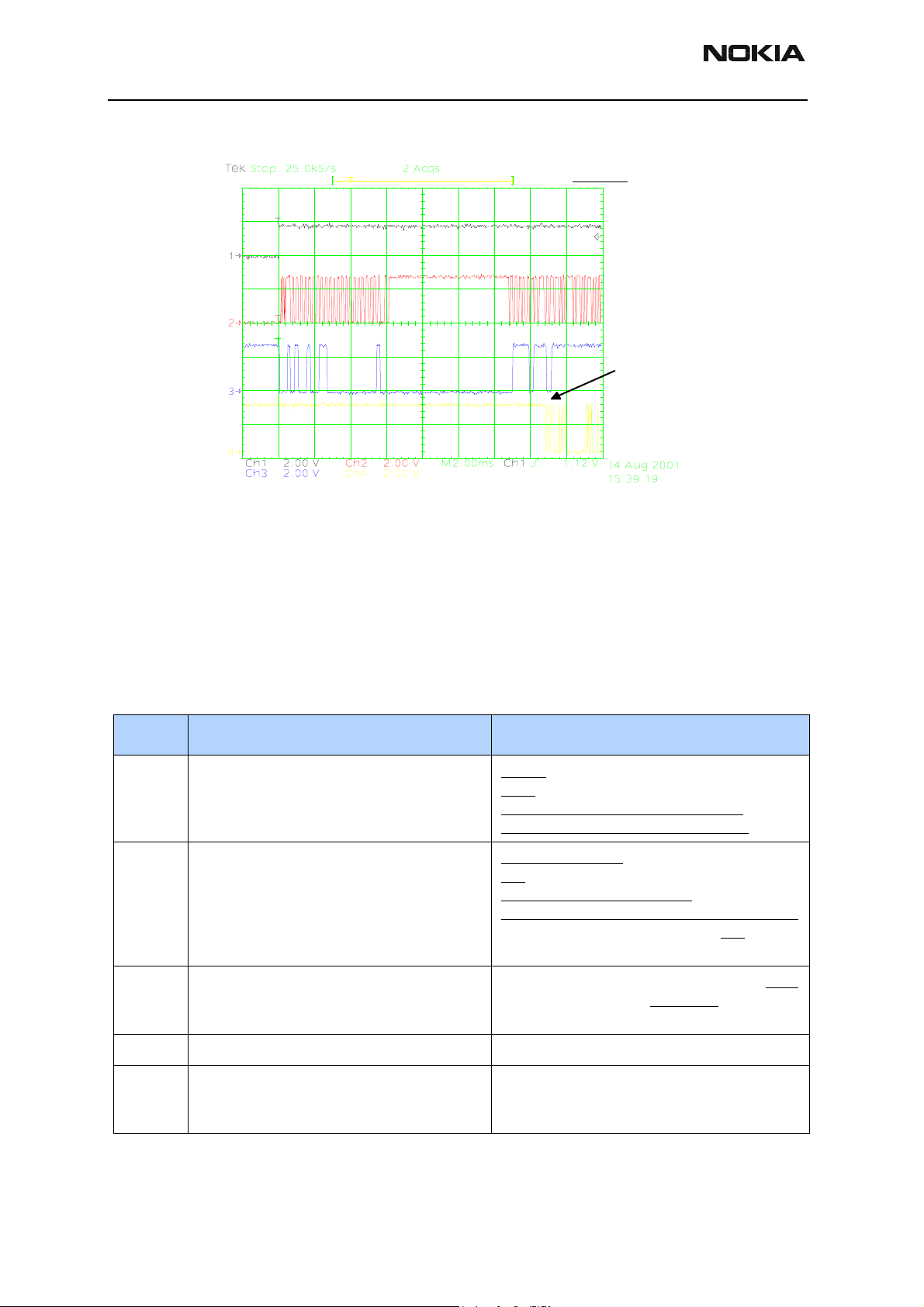
FM Radio Signals After Radio On
Figure 28: Radio signals after radio on
Page 32 ©2004 Nokia Corporation Confidential Issue 1 02/2004
Page 33

RM-11
CC Technical Documentation Troubleshooting - Baseband
Accessories
The RM-11 is designed to support Tomahawk and Universal Headset accessories,
differential and single-ended, respectively. Detection of Tomahawk accessories is done
through the ACI signal where the Universal Headset is detected on GenIO (21).
You can perform the following functions in Tomahawk accessories:
These modes are explained in the following sections.
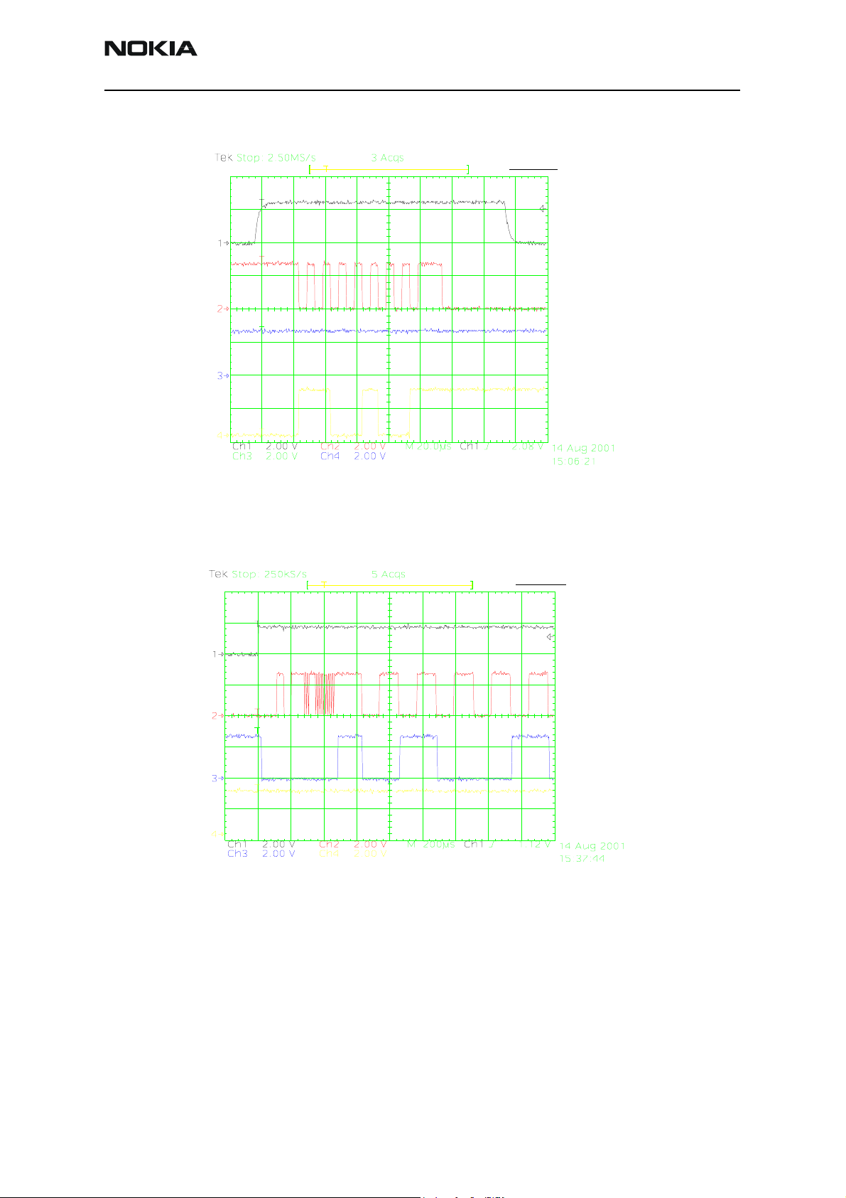
Charging
Charging through Tomahawk is done the same way as through the charger connector.
Pin 1 of the Tomahawk is physically connected the charger connector. When the phone is
connected to the desktop charger (e.g., DCV-15) it is charged the same way as is done on
the charger connector.
The actual charging sequence can be seen in Figure 30. The channels in the figure are as
follows:
Figure 29: Pin out of the Tomahawk connector
• Charging
• Accessory detection
• FBUS communication
• USB communication
• Fully differential audio interface for mono and stereo outputs
• CH1 = Charging current across the .22 Ohm (R200) resistor on UEMK
• CH2 = Charger voltage measure at V100
• CH3 = Battery voltage measure at R200
•CH4 = PURX
Issue 1 02/2004 ©2004 Nokia Corporation Confidential Page 33
Page 34

RM-11
Troubleshooting - Baseband CC Technical Documentation
Notice in Channel 4 that PURX is released. This is when the phone operation goes from
RESET mode to POWER_ON mode.
Tomahawk Headset Detection
Accessory detection in Tomahawk is done digitally. The pins used for accessory detection
are as follows:
• Pin 2 (Charge GND)
• Pin 3 (ACI)
•Pin 4 (Vout)
Figure 30: Charging sequence
Page 34 ©2004 Nokia Corporation Confidential Issue 1 02/2004
Page 35

RM-11
CC Technical Documentation Troubleshooting - Baseband
FBus Detection
FBus communication in Tomahawk is done through the following lines:
• Pin 2 (Charge GND)
• Pin 3 (ACI)
•Pin 4 (Vout)
• Pin 6 (FBus Rx)
• Pin 7 (FBus Tx)
Figure 31: A waveform of digital accessory detection
Issue 1 02/2004 ©2004 Nokia Corporation Confidential Page 35
Page 36

RM-11
Troubleshooting - Baseband CC Technical Documentation
Figure 32: FBus communication in Tomahawk
Accessory Detection Though ACI
USB and Audio on (mono or stereo) and FM radio communication in Tomahawk are done
through the following signals:
Table 11: Accessory detection signals
USB Audio/FM
Pin 5 (USB Vbus) Pin 9 (XMic N)
Pin 6 (USB +) Pin 10 (SMIC P)
Pin 7 (USB -) Pin 11 (HSEAR N)
Pin 8 (Data GND) Pin 12 (HSEAR P)
Pin 13 (HSEAR R N)
Pin 14 (HSEAR R P)
Page 36 ©2004 Nokia Corporation Confidential Issue 1 02/2004
Page 37

RM-11
CC Technical Documentation Troubleshooting - Baseband
Figure 33: USB and Audio on (mono or stereo) and FM radio communication in Tomahawk
RUIM (SIM CAR)
RM-11 supports RUIM for China products. The following waveform can be used to verify
that sim_vcc; sim_i/o, sim_clk, and sim_rst signals are activated in the correct sequence
at power up. This picture can be taken when the RUIM is installed on the phone and
measures the signals when the phone is turned on. Figure 34 shows the proper waveforms when the interface is working. See Figure 36 on page 40 for the test point
locations.
Issue 1 02/2004 ©2004 Nokia Corporation Confidential Page 37
Page 38

RM-11
Troubleshooting - Baseband CC Technical Documentation
Figure 34: RUIM signal waveform
Page 38 ©2004 Nokia Corporation Confidential Issue 1 02/2004
Page 39

RM-11
CC Technical Documentation Troubleshooting - Baseband
Test Points
RM-11 BB test points, regulators, and BB ASICs.
Top View
Figure 35: Top view
Issue 1 02/2004 ©2004 Nokia Corporation Confidential Page 39
Page 40

RM-11
Troubleshooting - Baseband CC Technical Documentation
Bottom View
Figure 36: Bottom view
Page 40 ©2004 Nokia Corporation Confidential Issue 1 02/2004
Page 41

RM-11
CC Technical Documentation Troubleshooting - Baseband
Camera Test Points
Figure 37: Camera test points; top side under LCD module
Issue 1 02/2004 ©2004 Nokia Corporation Confidential Page 41
Page 42

RM-11
Troubleshooting - Baseband CC Technical Documentation
Top Troubleshooting Map
Top
P hone totally dead
NO
Flas h programming
does n't work
NO
P hone does n't start
up or phone is
jammed
NO
YES
YES
YES
Phone
dead
Flash
faults
Phone is
jammed
C harging does n't
work
NO
YES
Top page 2
Charger
faults
Page 42 ©2004 Nokia Corporation Confidential Issue 1 02/2004
Page 43

RM-11
CC Technical Documentation Troubleshooting - Baseband
Top 2
Audio faults
NO
Dis play o r L E Ds no t
working
NO
Keypad doesn't work
YES
YES
YES
Audio
faults
Dis play
faults
Keypad
faults
END
Issue 1 02/2004 ©2004 Nokia Corporation Confidential Page 43
Page 44

RM-11
Troubleshooting - Baseband CC Technical Documentation
Phone is Totally Dead
¾ If current is zero, check X100 solder and make
Phone is
dead
sure Vbatt connector makes contact.
¾ If current is too high, check for shorts.
¾ Make sure all BB regulators are at their
respective voltage levels (VANA, VIO, VCORE,
VFlash1, and VR3). See phone's top view
diagram for test points.
Phone current is
zero or too high?
NO
Phone current is
<=30 mA
NO
Phone current is
35 mA
YES
YES
YES
NO
¾ Make sure the System Clk is 19.2MHz and that
the Sleep Clk is 32KHz
¾ Make sure PURX and SleepX signals are high
(1.8V)
Is phone flash
programming OK?
NO
YES
Phone is
jammed
Flash
faults
Is phone in Local
Mode?
YES
Check BSI line X100,
NO YES
R202, R203, C230.
Are they OK?
NO
Change UEM
Repair
OK restart
Page 44 ©2004 Nokia Corporation Confidential Issue 1 02/2004
Page 45

RM-11
CC Technical Documentation Troubleshooting - Baseband
Flash Programming Does Not Work
Flash
faults
Phone does not set
Flashbus TXD line
high after startup
NO
Change UEM
Does the phone set
Flashbus TXD line
low after the line has
been high?
YES
Flash
faults,
page 2
Measure BSI pulse
YES NO
during Flash
programming. Is it
OK?
YES
Measure FBusRx
(2.78V) signal during
flash programming
from production
pattern and test
point TP03 (1.8V). Is
it the same?
YES NO
Measure test point
FBusTx (TP05) (1.8V)
and production
pattern signal
FBusTxO (2.78V)
during flash
programming. Are
NO
they the same?
Measure MBusRx
YES
(2.78V) and test
point TP01 (1.8V).
Are they the same?
YES
NO
NO
NO
Check BSI line X100,
C230, R203, R202
Reflow or change
UEM
Reflow or change
UPP
Is there a pulse on
TP05?
YES
Is there a pulse on
FBusTx?
NO
Reflow or change
UEM
Reflow or change
UEM
Issue 1 02/2004 ©2004 Nokia Corporation Confidential Page 45
Page 46

RM-11
Troubleshooting - Baseband CC Technical Documentation
Flash
faults,
page 2
Reflow the flash. Is it
OK?
NO
Can you read
manufacturer ID and
device ID?
NO
Reflow or
change flash.
YES
Is phone totally
dead?
NO
Phone doesn't start
up or phone is
jammed?
NO
Reflow the UPP. Is it
OK?
YES
YES
Phone is
Phone is
jammed
NO
dead
Retest
Page 46 ©2004 Nokia Corporation Confidential Issue 1 02/2004
Page 47

RM-11
CC Technical Documentation Troubleshooting - Baseband
Phone is Jammed
Phone is
jammed
Measure VIO,
VCORE, VFlash1,
VANA, and VR3
voltages. Are they
OK?
YES
Measure 32kHz
Sleep Clk from test
point J974 and J975.
Is it OK?
Check VBATT, VIO,
VCORE, VFlash1,
VANA , VR3
capacitors. Are they
NO
OK? (See phone top
view diagram for
capacitor locations)
NO
NO NO
Measure 32kHz Clk
crystal. Is it OK?
YESYES
YES
Check BSI/BTEMP
lines and VBATT
lines. If OK, change
UEM
Repair
Change B200
Reflow or change
UEM
Measure 19.2MHz RF
Clk at test point
C524. Is it OK?
YES
Measure PURX
(TP16) and SleepX
(TP10). Are they high
(1.8V)?
YES
Phone is
jammed,
page 2
YES
NO
NO
Is PURX
OK?
YES
Is SleepX
OK?
Measure 19.2MHz
Clk coming from
VCTCXO at C502. Is
it OK?
YES
Check R517, R521,
and D527. Is it OK?
NO
NO
NO
NO
YES
Check G503, C505,
C520, C503, R511,
R512, R518, R553. If
OK, change G501.
Change UPP
Repair
Change UEM
Change UPP
Issue 1 02/2004 ©2004 Nokia Corporation Confidential Page 47
Page 48

RM-11
Troubleshooting - Baseband CC Technical Documentation
Power Does Not Stay on or the Phone is Jammed
Phone is
jammed,
page 2
Phone shutdown
after 32 seconds
NO
Measure DBusClk
(9.6MHz), Data, and
EnX signals at TP13,
TP11, TP09. Is it OK?
YES
Read phone info. Is
it OK?
YES
Retest
YES NO
Has the phone been
flashed?
YES
Measure watchdog
signal Cbus from
test points TP15,
NO
TP08, TP05. Is it OK?
Reflow or
change
UPP
NO
Measure FBusRx
signal during phone
info read from test
point TP03. Is it OK?
YES
Measure FBusTx
signal during phone
info read from test
point TP05. Is it OK?
YES
NO
NO
Flash the phone
Reflow or change
UPP and re-flash
Reflow or change
UEM and re-flash
Reflow or change
UEM
Reflow or change
UPP
NO
Reflow or change
UEM
YES
Page 48 ©2004 Nokia Corporation Confidential Issue 1 02/2004
Page 49

RM-11
CC Technical Documentation Troubleshooting - Baseband
Charger Faults
Charger
faults
Connect charger.
Make sure battery is
connected.
Battery bar doesn't
work (scroll)
YES
Measure voltage
over V100. Is it > 3.0
Vdc?
YES
Read BTEMP value.
Is it ~25C (0319)?
YES
Remove (fuse) F100
and measure
current.
Is it ~850mA? Make
sure to use an ACP9
charger
NO
NO
NO
NO
Retest
Check X102, F100,
L100, V100, C106,
C110
Change UEM
Change UEM
YES
Retest
Issue 1 02/2004 ©2004 Nokia Corporation Confidential Page 49
Page 50

RM-11
Troubleshooting - Baseband CC Technical Documentation
Audio Faults
Earpiece
Audio
faults
Is the earpiece
working?
YES
NO YES
Change earpiece. Is
it working now?
NO
Set phone in Local Mode. Use
Phoenix "Baseband Audio
Control" and set the following:
Enable Tx, Enable Rx, Select
MIC2 (0dB), Enable earpiece,
and enable digital loopback
only. Inject a 1KHz sine signal
20mVp-p on XMIC.
Is the signal coming
out of the UEM on
EARP and EARN?
NO
Retest
Check L102, C152, C156,
C151, C154, C153, C170,
R151, R155, R152, R150,
and R153. If OK, change
the UEM.
Audio
faults,
page 2
YES
Check R177, R178,
and R179. If OK,
then change the
earpiece.
Page 50 ©2004 Nokia Corporation Confidential Issue 1 02/2004
Page 51

RM-11
CC Technical Documentation Troubleshooting - Baseband
Microphone
Audio
faults,
page 2
Is the microphone
working?
YES
Audio
faults,
page 3
Change the
NO YES
microphone. Is it
working now?
NO
Set phone in Local Mode. Use
Phoenix "Baseband Audio
Control" and set the following:
Enable Tx, Enable Rx, Select
MIC1, Enable HF only
(differential). Talk through the
microphone.
Measure MICB1
voltage from MICP
NO
pads on bottom
connector.
Is it ~2.1V?
YES
NO
Is the signal going to
the UEM at MIC1P
and MIC1N at R172?
YES
Is the signal going
NO
out of the UEM at
XEAR, pin 11, 12, 13,
and 14 on the
bottom connector
(X101)?
YES
Retest
Check connections
at C175 and R170. If
OK, change UEM.
Check connections
at R171, R172, R170,
R173, C173, C174,
C175, C170, C171,
C172. If OK, change
microphone.
Check L103, L104,
N150, C160, C161,
C169, C166, C168,
C164, C180, C181,
C183, C184, C185,
C112, C113, C114,
C115, R163, R976,
R977, R165, R164,
R112, R113. If OK,
change UEM.
Retest
Issue 1 02/2004 ©2004 Nokia Corporation Confidential Page 51
Page 52

RM-11
Troubleshooting - Baseband CC Technical Documentation
Vibra
Audio
faults,
page 3
Measure VBATT
Is Vibra working?
NO NO
Set phone in Local Mode. Use Phoenix
"Message Sender" and navigate as
follows: DEV_HOST-->DEV_PC-->
ACC_VIBRA_CTRL_REQ. Select
voltage pin 1 of
M300. Is it OK?
YES
PN_ACCESSORY-->
PN_OBJ_ROUTING_REQ-->
PN_OBJ_PC->UTID_100-->
"ACC_ON" and click "Send"
Check VBATT line
YES
END
Measure the UEM
signal on pin 2 of
M300. Is the signal
OK?
YES
NO
Change the UEM
Change Vibra
Page 52 ©2004 Nokia Corporation Confidential Issue 1 02/2004
Page 53

RM-11
CC Technical Documentation Troubleshooting - Baseband
Display Faults
Display
faults
Are the Keyboard
and LCD LEDs
turned on when
phone is turned on
or when making a
phone call?
NO NO
Set phone to Local Mode. Use
Phoenix "Message Sender" and
navigate as follows: DEV_HOST-->
OBJ_ROUTING_REQ-->OBJ_PC-->
UTID-->LIGHT_CONTROL_REQ-->
LIGHT_CONTROL_TARGER_KBD.
Select "LIGHT_STATE_BLINK" and
Measure VBATT
voltage at R315.
Is it OK?
YES
DEV_PC-->PN_LIGHT-->
click "Send"
Check VBATT line at
X100 connector and
C109
YES
Display
faults,
page 2
Measure the driver
signal KLIGHT at
R304.
Is signal OK?
YES
NO
Change UEM
Check N300, L300,
V300, C302, C303,
C304, R300, R307,
R315, R316, R317,
and X301 connector
Issue 1 02/2004 ©2004 Nokia Corporation Confidential Page 53
Page 54

RM-11
Troubleshooting - Baseband CC Technical Documentation
Display
faults,
page 2
Does the Display
start?
YES
Try changing display
NO YES
module. Does it
work?
NO
Set phone in Local Mode. Use Phoenix
"Message Sender" and navigate as
follows: DEV_HOST-->DEV_PC-->
PN_TEST-->OBJ_ROUTING_REQ-->
OBJ_PC-->UTID-->
TEST_UI_TEST_REQ-->
TEST_DISPLAY_SET-->NUM_SB-->
TEST_SB_UI_DISPLAY_PATTERN-->
SB_LENGTH. Select
"TEST_PATTERN_ALTPIXELS" and
click "Send"
Check VIO and VFlash1 at X302.
Also, check LCD signals LCDCSX
(pin5), LCDCLK (pin4), LCDSDA
(pin3), and LCDRESX (pin2) at
X302. Is signal OK? (Refer to
Display section)
NO
Retest
Change UPP
END
YES
Change
Display
Page 54 ©2004 Nokia Corporation Confidential Issue 1 02/2004
Page 55

RM-11
CC Technical Documentation Troubleshooting - Baseband
Keypad Faults
Power Key
Keypad
faults
Is the power key
working?
YES
Keypad
faults,
page 2
NO NO
Measure voltage at
R306. Is it high?
YES
Measure voltage at
R306 when power
key is pressed. Is it
low?
NO
YES
Check S302, C310,
and R306. If OK,
change UEM
Retest
Change S302
Issue 1 02/2004 ©2004 Nokia Corporation Confidential Page 55
Page 56

RM-11
Troubleshooting - Baseband CC Technical Documentation
UI Modules
Keypad
faults,
page 2
Are UI modules keys
working?
YES
NO
Change keypads
module. Is it
working?
NO
Measure ROW0-4
(P10-P15) signals
between UPP and
X301. Are they
~1.8V?
YES
Measure COL1-4
(P01-P04) signals
between UPP and
X302. Are they
~1.8V?
YES
NO
NO
Retest
Make sure there are
no shorts on Z300. If
OK, change UPP
Change Z300
Make sure there are
END
YES
no shorts on Z300. If
OK, change UPP
Page 56 ©2004 Nokia Corporation Confidential Issue 1 02/2004
Page 57

RM-11
CC Technical Documentation Troubleshooting - Baseband
FM Radio
FM Radio
faults
Is the FM radio
working?
YES
Does the FM radio
produce a "Bong"
sound when
changing channels
(frequencies)?
YES
Check soldering
under C358/R359/
R360/C362. If not
working, then
change FM radio
chip (N356)
NO
NO
END
Power on the phone
and turn FM radio on
by Phoenix
YES
Measure VFlash2
(VCCD/VCCA/
VCCVCO) at C359/
C372/L357. Is it
2.8V?
YES
Measure FM1=1.8V,
FM2=11 Khz,
FM3=1.8V, and
FM4=32 Khz. Is it
OK?
YES
Measure FMANT at
L358. Is it 1.0V?
YES
FM
Radio
faults 2
NO
NO
Check solder on
NO
N356, X101, and
replace N356 if not
working.
NO
Check VFlash2 line
Change UPP (D400)
Check L351, L358,
C367, C378, C379,
C112, C113, C114,
C115. If OK, check
Tomahawk
connector (X101) on
pin 11, 12, 13, 14
NO
(From
Radio
Faults 2)
NO
Issue 1 02/2004 ©2004 Nokia Corporation Confidential Page 57
Page 58

RM-11
Troubleshooting - Baseband CC Technical Documentation
FM Radio
faults 2
Measure VREF at
C365. Is it 1.6V?
YES
Measure VAFL/VAFR
at C164/C168. Does
it have an audio
signal?
Retest
YES
Is FM Radio
working?
NO
NO
Check C365
Change FM Radio
chip (N356)
NO
YES
END
Page 58 ©2004 Nokia Corporation Confidential Issue 1 02/2004
Page 59

RM-11
CC Technical Documentation Troubleshooting - Baseband
Camera
Camera
faults
Power on the phone
and turn camera on
by Phoenix or UI
menu
YES
NO
Make sure soldering
on X970 and D970 is
OK and check
PUSL(1) on R997. Is
it high?
YES
Check VDIG voltage
at C983
YES
Check VFlash2
voltage at C981,
C971, C970
YES
Check whether CE is
high
NO
Check D200 and
NO
replace it when D200
keeps low
NO
Replace N970
regulator
Check D200 and
replace it if no
output from UEM
Check D400 and
NO
replace it if this
GenIO 5 is low all
the time
Try test again
Issue 1 02/2004 ©2004 Nokia Corporation Confidential Page 59
Page 60

RM-11
Troubleshooting - Baseband CC Technical Documentation
Flashlight
Flashlight
faults
Are the flashlight
LEDs turned on
when the phone is
turned and when
pressing the * key?
YES
NO
Measure VBATT
voltage at R315. Is it
OK?
YES
Measure the driver
signal DLIGHT at
V317 an dV301. Is
the signal OK?
Check VBATT line at
NO
NO
X100 connector and
Change the UEM
C109
Flashlight
OK
GPS Module
Overview
The GPS circuitry utilizes RF signals from satellites stationed in geosynchronous orbit to
determine longitude and latitude of the handset. The GPS circuitry is completely separate
from the CE circuitry and is located almost exclusively on the secondary side of the PWB
underneath the display module (see Figure 38).
YES
Check N300, V301,
L300, C302, C303,
C304, R300, R307,
R315, R316, R317
YES
Check solder joints
at V304 and V303. If
bad, replace LEDs
Page 60 ©2004 Nokia Corporation Confidential Issue 1 02/2004
Page 61

RM-11
CC Technical Documentation Troubleshooting - Baseband
Figure 38: GPS block diagram
The basic GPS BB troubleshooting method is to put the GE and CE in the proper mode
and check to make sure that necessary inputs from the CE are good (power, clock, etc.).
Then, ensure that these inputs produce the proper outputs. Because of the large level of
integration (most functionality is contained in the two ASIC chips), the amount of diagnostics one is able to do is limited.
Prior to performing diagnostics, perform a visual inspection on the GPS circuitry to see if
the problem is physical (dislodged parts, corrosion, poor solder joints, etc.)
Issue 1 02/2004 ©2004 Nokia Corporation Confidential Page 61
Page 62

RM-11
Troubleshooting - Baseband CC Technical Documentation
Vcore at 1.5V? Troubleshoot CE power supply
Vio at 1.8V?
GPS_RF_CLK
(19.2MHz) OK?
GPS_EN_RESET is
held high?
GPS_SLEEPCLK
(32.768KHz) OK?
VRF_GPS OK?
NO NO
GPS_CLK (16.368MHz) OK? Replace TXCO or GPS RF ASIC
NO
NO
NO
NO
VRF_GPS regulator
enable line low?
NO
Troubleshoot CE VCTCXO
circuit
BB ASIC being held in reset,
troubleshoot source in the CE
Troubleshoot CE sleep clock
circuit
Replace regulator
(N052)
Test Mode 1 OK? Replace GPS BB ASIC
CE sending code download
signals?
SPI interface active? Replace GPS BB ASIC
NO
NO
NO
NO
Determine why CE not sending
download signals
Replace GPS RF ASICRF Data and clock?
Debug RF front end
Figure 39: GPS troubleshooting flowchart
Page 62 ©2004 Nokia Corporation Confidential Issue 1 02/2004
 Loading...