

Page 1

CC Technical Documentation
RM-11 Series Transceivers
Troubleshooting - RF (Part 2)
Issue 1 02/2004 Confidential ©2004 Nokia Corporation
Page 2

RM-11
Troubleshooting - RF (Part 2) CC Technical Documentation
Contents Page
Synthesizer Troubleshooting.......................................................................................... 3
Synthesizer Setup Using Phoenix ................................................................................4
VCTCXO Troubleshooting .........................................................................................4
UHF Synthesizer Troubleshooting ..............................................................................6
UHF Synthesizer Schematic ........................................................................................6
UHF Synthesizer Layout .............................................................................................7
UHF Frequency is Incorrect...................................................................................... 7
RX VHF (Batman LO) Schematic ...............................................................................7
RX VHF Layout ..........................................................................................................8
Incorrect RX VHF Frequency................................................................................... 9
TX VHF Schematic .....................................................................................................9
TX VHF Layout .........................................................................................................10
Incorrect TX VHF Frequency ................................................................................. 10
TX Troubleshooting..................................................................................................... 11
Transmitter Schematic 1 ............................................................................................11
Transmitter Schematic 2 ............................................................................................12
TX Troubleshooting Using Phoenix ..........................................................................13
PCS Band TX Probe Points .......................................................................................15
Cell and AMPS Band TX Probe Points .....................................................................16
TX AMPS Troubleshooting Using Phoenix ..............................................................17
RX Troubleshooting..................................................................................................... 18
Receiver Schematic ...................................................................................................18
Turning on Rx Path Using Phoenix ...........................................................................19
Switching Rx Gain States Using Phoenix .................................................................20
Receiver IF Troubleshooting Layout .........................................................................21
Receiver RF Troubleshooting Layout .......................................................................22
Receiver DC Troubleshooting Layout .......................................................................23
Receiver DC Troubleshooting Layout .......................................................................24
Alfred Receiver Troubleshooting ..............................................................................25
Receiver DC Troubleshooting Alfred ........................................................................26
Control Signals at RF-BB Interface ...........................................................................26
Back Panel Control Signals RF-BB Interface ...........................................................27
Page 2 ©2004 Nokia Corporation Confidential Issue 1 02/2004
Page 3
RM-11
CC Technical Documentation Troubleshooting - RF (Par t 2)
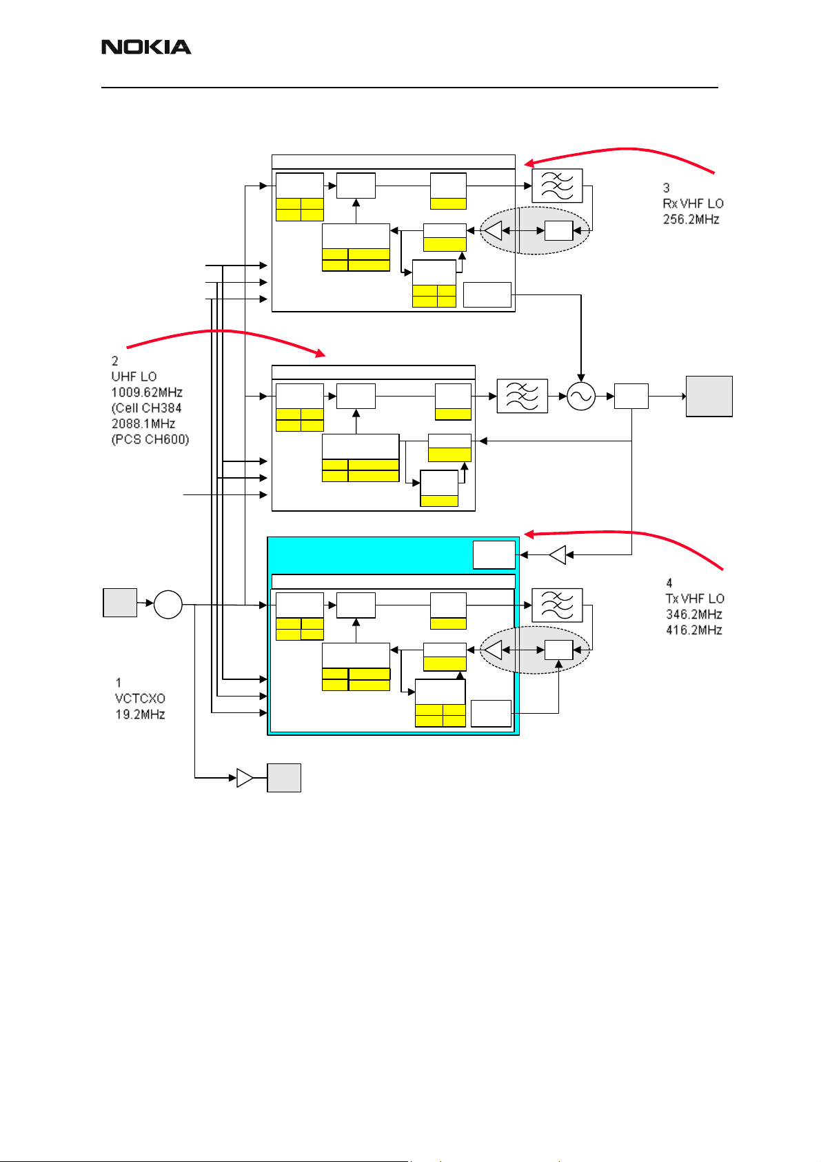
Synthesizer Troubleshooting
RX VHF Synthesizer
128
128PCS
Phase
Detector
9-Bit B
Counter
Charge
Pump
2 mA
Prescaler
53Cell
53PCS
32/33
5-Bit A
Counter
VCO Band
12Cell
Control
12PCS
RX VHF VCO
Tank
RF_BUS_CLK
RF_BUS_DATA
RF_BUS_EN1X
Reference
Divider
Cell
SYNTH_LE
AFC
UEM
VCTCXO
19.2 MHz
Reference
Divider
Cell
Reference
Divider
Cell
PCS
UHF Synthesi zer
384PCS
640
384
Cell
PCS
Phase
Detector
13-Bit B
Counter
1038 - 1064Cell
1286 - 1323PCS
TX VHF Synthesizer
Phase
Detector
9-Bit B
Counter
360
260
5-Bit A
Counter
0 - 31
Prescaler
5-Bit A
Counter
Cell
PCS
Charge
Pump
4 mA640
Prescaler
32/33
Charge
Pump
2 mA
32/33
20
4
SSB
Mixers
VCO
Band
Control
TX VHF VCO
Tank
UHF VCO
Splitter
UHF LO
RX
FRONT
END
UPP
Figure 1: Synthesizer troubleshooting diagram
Issue 1 02/2004 ©2004 Nokia Corporation Confidential Page 3
Page 4
RM-11
Troubleshooting - RF (Part 2) CC Technical Documentation
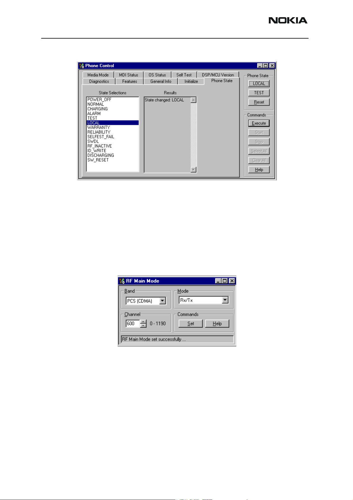
Synthesizer Setup Using Phoenix
Figure 2: Phone Control dialog box
1. Click the LOCAL button on the Phone Control dialog box.
2 Use the following settings for the fields on the RF Main Mode dialog box:
• UHF: Use RX/TX mode in PCS and Cell band. This allows for checking power
to both RX and TX circuits. Typically, use channel 384 in Cell band and 600 in
PCS band.
• RX VHF: Use RX mode; one band is enough.
• TX VHF: Use RX/TX mode in PCS and Cell band.
Figure 3: RF Main Mode dialog box
3. Click the Set button.
Note: Make sure the “RF Main Mode set successfully...” message appears.
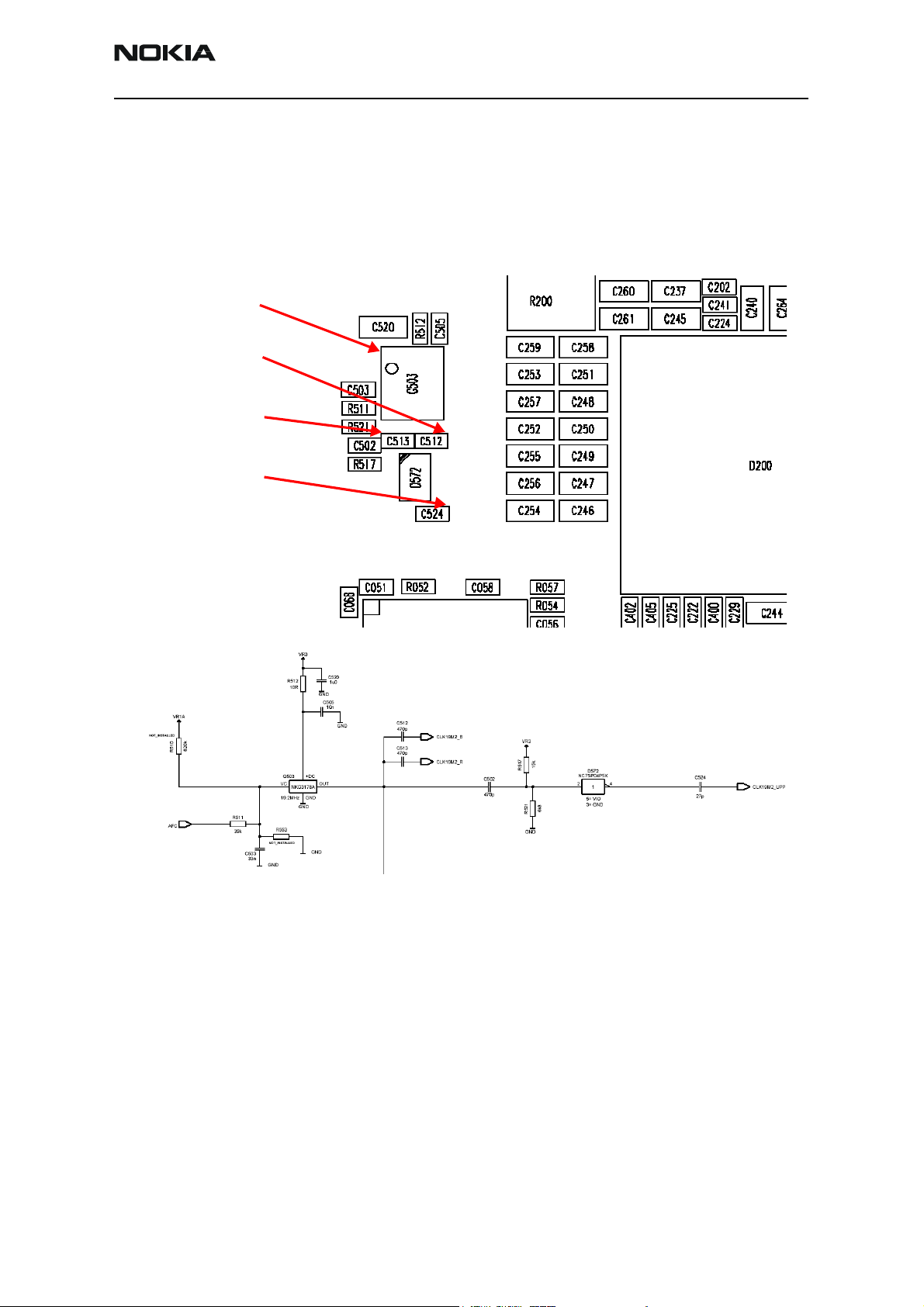
VCTCXO Troubleshooting
The VCTCXO frequency is 19.2MHz, which is the reference signal. Without 19.2MHz, the
phone will not power up. This signal goes to Batman, Robin, UHF PLL, and also to the UPP
via a buffer amplifier (D572).
Page 4 ©2004 Nokia Corporation Confidential Issue 1 02/2004
Page 5
RM-11
CC Technical Documentation Troubleshooting - RF (Par t 2)
Check for the presence of the signal at the following points (use a high-impedance
RF probe):
• CLK19M2_B, clock reference to Batman, should be +4.5dBm
• CLK19M2_R, clock reference to Robin, should be +4.5dBm
• CLK19M2_UPP, clock reference to UPP, should be +7.5dBm
VCTCXO
To Batman PLL
19.2 MHz @ +4.5 dBm
(CLK19M2_B)
To Robin PLL
19.2 MHz @ +4.5 dBm
(CLK19M2_R)
To Baseband UPP
19.2 MHz @ +7.5 dBm
(CLK19M2_UPP)
VR3 = 2.78VDC
VIO = 1.8VDC
Figure 4: Presence of signal test points
If you do not see the VCTCXO signal at any of these points, check the voltages at the
following supply lines:
• VR3, main supply line for VCTCXO circuitry, should be 2.78VDC
• VIO, supply line for buffer amplifier, should be 1.8VDC
Issue 1 02/2004 ©2004 Nokia Corporation Confidential Page 5
Page 6
RM-11
Troubleshooting - RF (Part 2) CC Technical Documentation
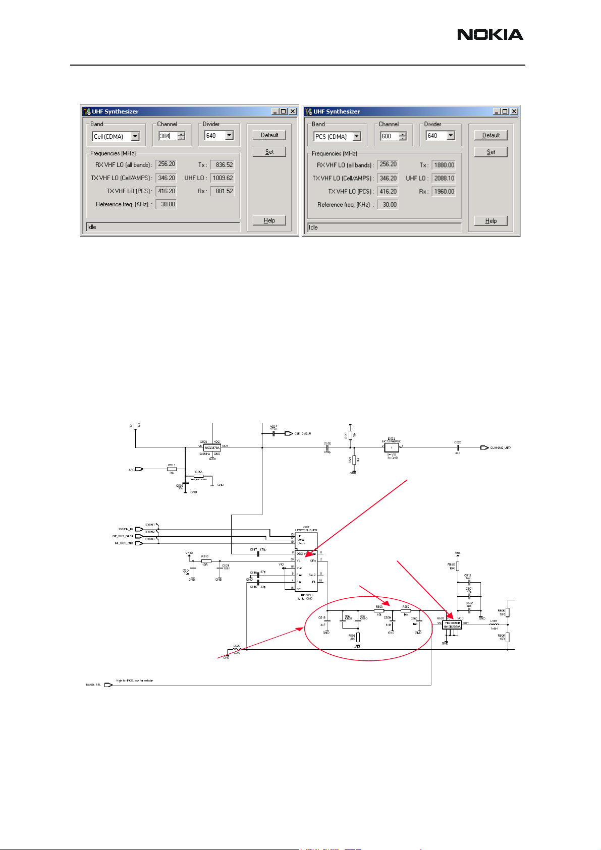
UHF Synthesizer Troubleshooting
Figure 5: UHF Synthesizer dialog box for Cell (left) and PCS (right) bands
UHF LO frequency varies with channel and can be quickly calculated using the
UHF Synthesizer dialog box on the RF menu. Check to see if the LO is actually locked.
Set a channel and check the status of the UHF LO within a very narrow span of 100KHz.
You should see the LO virtually immobile. Nominal UHF LO signal levels are measured
with an RF probe (see the following figures). If you do not see the presence of any LOs,
check DC voltages at the following locations:
• R513, VR1A, supply line for UHF PLL IC. Should be 4.76VDC
• R515, VR4, supply line for VCO IC. Should be 2.76VDC
UHF Synthesizer Schematic
UHF PLL IC
Dual Band VCO
Lock voltage
Loop filter components
Figure 6: UHF synthesizer schematic
Page 6 ©2004 Nokia Corporation Confidential Issue 1 02/2004
Page 7
RM-11
CC Technical Documentation Troubleshooting - RF (Par t 2)
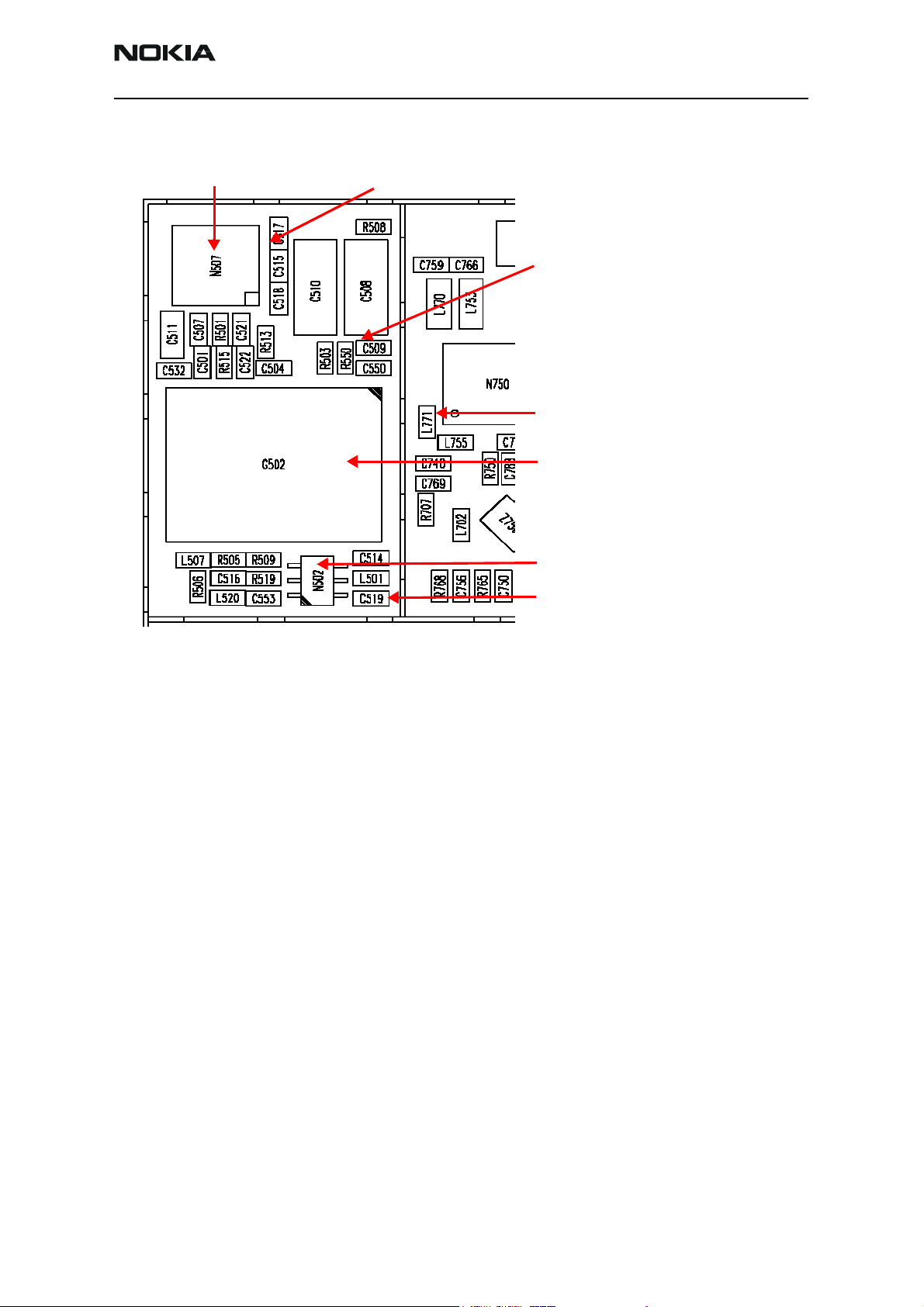
UHF Synthesizer Layout
VCTCXO reference probing point
UHF PLL IC LMX2310
19.2 MHz @ +4.5 dBm
Lock voltage:
DC between 1V and 3V
RX LO Input to Alfred
Cell channel 384: 1009.62 MHz @ -2.5 dBm
PCS channel 600: 2088.10 MHz @ -12 dBm
Dual-band UHF VCO
Figure 7: UHF synthesizer layout
UHF Frequency is Incorrect
Possible causes:
• Power supplies to PLL IC (N507) are missing or low
• Loop filter components missing or incorrectly installed
• 19.2MHz reference clock missing or low
• Programming is incorrect
• Component failure (VCO or PLL IC)
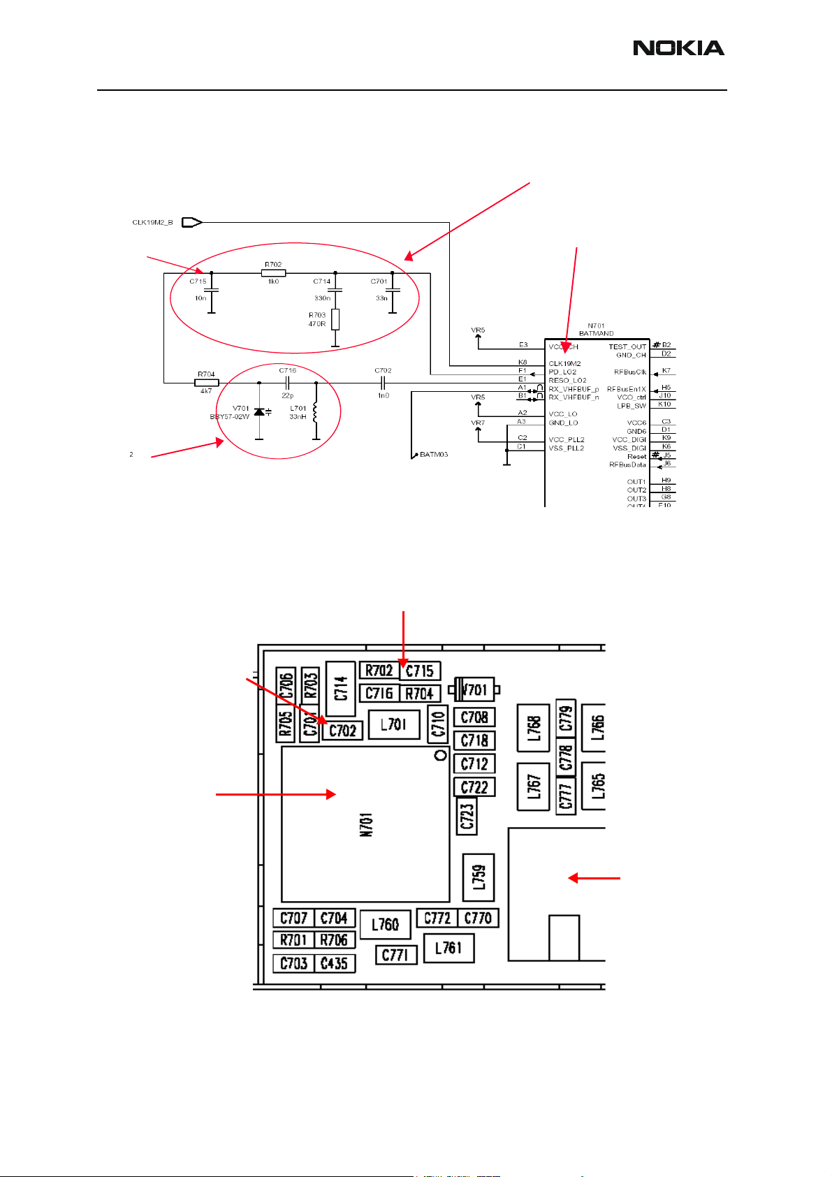
RX VHF (Batman LO) Schematic
• Operates at a fixed frequency of 256.2MHz. It is the second LO for
down-conversion to I and Q for baseband processing. Refer to the frequency
plan.
TX LO Buffer
RF probe point, TX LO output levels:
Cell channel 384: 1009.62 MHz @ -0.5 dBm
PCS channel 600: 2088.10 MHz @ -20 dBm
• Monitor probing point at C702 for Batman LO. A locked and stable 256.2MHz
with an amplitude of ~= -2.5dBm should be observed on the spectrum analyzer.
• Monitor control voltage at C715. The control voltage at locked state should be
between 1.2 and 1.7VDV for the proper operation of Batman LO.
Issue 1 02/2004 ©2004 Nokia Corporation Confidential Page 7
Page 8
RM-11
Troubleshooting - RF (Part 2) CC Technical Documentation
Loop filter components
Lock voltage
Resonator
RX VHF Layout
PLL in Batman
Figure 8: RX VHF (Batman LO) Schematic
Lock Voltage Probing Point:
DC voltage between 1V and 2V
RF probing point
256.2 MHz @ -2.5 dBm:
Batman IC with
Integrated PLL
CDMA IF filter
Figure 9: RX VHF layout
Page 8 ©2004 Nokia Corporation Confidential Issue 1 02/2004
Page 9
RM-11
CC Technical Documentation Troubleshooting - RF (Par t 2)
Incorrect RX VHF Frequency
Possible causes:
• Power supplies to PLL portion of Batman IC (N701) missing or low (VR7)
• Loop filter or resonator components missing or incorrectly installed
• 19.2MHz reference clock missing or low (C512)
• Programming is incorrect
• Component failure (PLL IC)
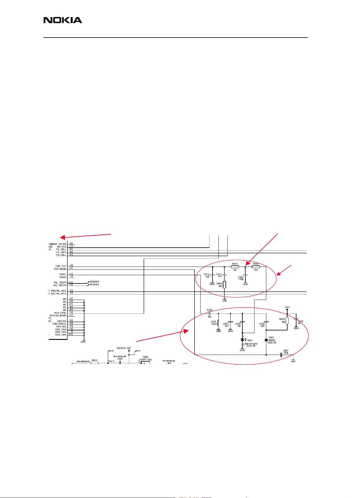
TX VHF Schematic
There are two fixed LOs — 346.2MHz for Cell band and 416.2MHz for PCS band. This is
the first LO for up-conversion. Refer to the frequency plan.
Monitor the probing point at C638 with a high-impedance RF probe for Robin LO.
A sufficiently strong and stable signal should be observed on the spectrum analyzer.
Monitor control voltage at C632. At this control voltage, the Robin LO is locked (it should
be between 1.2 and 1.8VDC).
Lock voltage
Robin
Loop filter
Resonator
Figure 10: TX VHF Schematic
Issue 1 02/2004 ©2004 Nokia Corporation Confidential Page 9
Page 10

RM-11
Troubleshooting - RF (Part 2) CC Technical Documentation
TX VHF Layout
RF Probing Point:
Cell: 346.2 MHz @ -6.5 dBm
PCS: 416.2 MHz @-6.5 dBm
Robin IC with integrated PLL
Lock Voltage Probing Point:
DC voltage between 1V and 2V
Incorrect TX VHF Frequency
Possible causes:
• Power supplies to PLL portion of Robin IC (N601) missing or low (VR3)
• Loop filter or resonator components missing or incorrectly installed
• 19.2MHz reference clock missing or low
• Programming is incorrect
• Component failure (PLL IC)
Figure 11: TX VHF Layout
Page 10 ©2004 Nokia Corporation Confidential Issue 1 02/2004
Page 11

RM-11
CC Technical Documentation Troubleshooting - RF (Par t 2)
TX Troubleshooting
RX
PCS
PCS
Duplexer
Duplexer
WHIP
WHIP
ANT.
ANT.
RF Conn
RF Conn
Internal
Internal
ANT.
ANT.
Cell
Cell
Duplexer
Duplexer
Diplexer
Diplexer
RX
RX
RX
Isolator
Isolator
Isolator
Isolator
PCS PA
PCS PA
Cell PA
Cell PA
Switch
Switch
Split Band
Split Band
Saw Filter
Saw Filter
Hi BAND
Hi BAND
Lo BAND
Lo BAND
CELL
CELL
SAW
SAW
Filter
Filter
PCS Driver
PCS Driver
Detector
Detector
TX_RF_AGC
TX_RF_AGC
( UPP )
( UPP )
Cell Driver
Cell Driver
PCS
PCS
Balun
Balun
Cell
Cell
Balun
Balun
P_DET
P_DET
P_REF
P_REF
PCS
PCS
DVR
DVR
CELL
CELL
DVR
DVR
UP CONV
UP CONV
Current Mirror
Current Mirror
PA_AGC
PA_AGC
Figure 12: RM-11 TX system block diagram
UHF LO
UHF LO
( UPP )
( UPP )
IF AGC
IF AGC
PWROUT
PWROUT
(UEM)
(UEM)
19.2
19.2
CLK
CLK
MHz
MHz
VHF PLL
VHF PLL
TX_ IF_AGC
TX_ IF_AGC
( UPP )
( UPP )
Filter &
Filter &
Resonator
Resonator
CLK
CLK
En CLK
En CLK
DATA
DATA
SIO
SIO
VHF SYNTH
VHF SYNTH
Div By 2
Div By 2
I/Q
I/Q
MODBBFilter
MODBBFilter
Robin TX Upconverter
Robin TX Upconverter
2
2
I
I
inputs
inputs
Q
Q
2
2
(UEM)
(UEM)
Setup the phone in Local Mode with the appropriate band, channel, RHO on, and PDM
settings. An Agilent call box 8960 is recommended to measure TX power at the RF
connector. The numbers in Figure 13 and Figure 14 indicate the general RF signal flow
and probing locations. More details are given in the following sections.
Transmitter Schematic 1
PCS Driver
11
PCS split-band SAW Filter
PCS switch
22
Cell Driver
11
Cell SAW Filter
22
PCS Band
Cell Band
Robin TX Up- converter
Figure 13: Transmitter Schematic 1
Issue 1 02/2004 ©2004 Nokia Corporation Confidential Page 11
Page 12

RM-11
Troubleshooting - RF (Part 2) CC Technical Documentation
Transmitter Schematic 2
5
55
PCS Duplexer
4
3
33
PCS PA
PCS PA
Cell PA
3
33
5
55
Cell PA
44
Power
Power
Detector
Detector
PCS Isolator
PCS Isolator
4
44
Cell Isolator
Cell Isolator
PCS Duplexer
Cell Duplexer
Cell Duplexer
Diplexer
Diplexer
RF
RF
Connector
Connector
Figure 14: Transmitter Schematic 2
Page 12 ©2004 Nokia Corporation Confidential Issue 1 02/2004
Page 13

RM-11
CC Technical Documentation Troubleshooting - RF (Par t 2)
TX Troubleshooting Using Phoenix
1. Use the Phone Control dialog box to turn the phone on.
2Click the Phone State tab.
3. Highlight Local, and click the Execute button. This will put the phone into Local
Mode.
Figure 15: Phone Control dialog box
4. Use the RF Main Mode dialog box to set the following fields:
•Band
• Channel
• Rx/Tx mode
PCS Band
Cell Band
Figure 16: RF Main Mode dialog box with PCS and Cell band values
Issue 1 02/2004 ©2004 Nokia Corporation Confidential Page 13
Page 14

RM-11
Troubleshooting - RF (Part 2) CC Technical Documentation
5. Click the Set button.
Note: Make sure the “RF Main Mode set successfully...” message appears.
6. Open the DSP menu and select the CDMA Control option.
7. Select the Rho ON check box, and click the Execute button.
Figure 17: CDMA Control dialog box
8. At this point you should be able to measure TX Pout at the RF connector using
the 8960 Call Box.
• Cell Band TX Pout = +11dBm
• PCS Band TX Pout = +12dBm
If you do not see these powers, start probing the TX path to find out where the
signal stops.
9. Adjust the PDM values using the RF PDM dialog box.
MAXMIN MIN
MAXMIN MIN
MAX MAX
MINMAX MAX
MIN
Figure 18: RF PDM dialog box
Note: If you do not measure the correct Tx power at the RF connector, then it is time to use
the RF probe and determine where the failure occurs.
Page 14 ©2004 Nokia Corporation Confidential Issue 1 02/2004
Page 15

RM-11
CC Technical Documentation Troubleshooting - RF (Par t 2)
10. Local Mode (either PCS channel 600 or Cell channel 384):
• PA Gain PDM = +220
•RF AGC PDM = -512
• IF AGC PDM = -105 (PCS), -135 (Cell)
With PDMs set to the above values:
• Phone TX Pout ≅ 23dBm (PCS)
Current ≅ 720mA (PCS)
• Phone TX Pout ≅ 25dBm (Cell)
Current ≅ 880mA (Cell)
PCS Band TX Probe Points
3
2
1
Figure 19: PCS band Tx probe points
PCS Duplexer
4
PCS PA
5
Issue 1 02/2004 ©2004 Nokia Corporation Confidential Page 15
Page 16

RM-11
Troubleshooting - RF (Part 2) CC Technical Documentation
Use the PDM settings from the previous section. Following are the approximate power
levels you should expect for the PCS band (Channel 600):
• C660 Output of Robin (N601), input to Hornet (N602)
Probed power ≅-2dBm (If not, then replace Robin)
• C627 Output of split-band filter (Z601)
(Gain ≅10.5dB – (filter loss 2.3dB) ≅ 8.2dB)
Probed power ≅ 7dBm (If not, then replace Hornet)
• C802 Output of the TX Switch (Loss ≅ 1dB)
Probed power ≅ +6dBm (If not, then replace the switch)
• C803 Output of PCS PA (use 10dB pad on probe or just sniff part)
Probed power ≅ +18dBm (If not, then replace the PCS PA)
• C809 IREF into PCS PA should be ≅ 2.7V (If not, trace back to Robin and then
to the BB)
Cell and AMPS Band TX Probe Points
1
2
3
4
5
Figure 20: Cell and AMPS band TX probe points
Page 16 ©2004 Nokia Corporation Confidential Issue 1 02/2004
Page 17

RM-11
CC Technical Documentation Troubleshooting - RF (Par t 2)
Use PDM settings from the previous section. Here are the approximate power levels you
should expect for CELL BAND (Channel 384):
• C677 Output of Robin, Input to the Tomcat Driver
Probed power ≅ -3dBm (If not, then replace Robin)
• Pin 6 of Tomcat Driver is the output (Gain ≅ 14dB)
Probed power ≅ +11dBm (If not, then replace Tomcat)
• C80 Output of the TX Saw filter (Loss ≅ 1dB)
Probed power ≅ +10dBm (If not, then replace the filter)
• R801 Output of Cell PA (use 10dB pad on probe or just sniff part)
Probed power ≅ +21dBm (If not, then replace Cell PA)
• C811 IREF into Cell PA should be ≅ 2.7V (If not, then trace back to Robin and then
to BB)
TX AMPS Troubleshooting Using Phoenix
Use the following steps to troubleshoot the TX AMPS using Phoenix:
1. In Local Mode/Main Mode, select AMPS Band.
2. Use PDM controls to adjust the PA, RF AND IF AGC.
Figure 21: AMPS Control dialog box
3. Local Mode:
• PA Gain PDM = 229
•RF AGC PDM = -416
• IF AGC PDM = -137
With PDMs set to the above values:
• Phone TX Pout ≅ +26dBm
Current ≅ 998mA
Note: If you do not measure the correct TX power at the RF connector, then repeat Cell band
Local Mode troubleshooting to find where the failure occurs. AMPS and Cell band share the
same TX path.
Issue 1 02/2004 ©2004 Nokia Corporation Confidential Page 17
Page 18

RM-11
Troubleshooting - RF (Part 2) CC Technical Documentation
RX Troubleshooting
PCS RF FILTER
AMPS
AMPS
IF
FILTER
IQ
DEMOD
ADC
I
PCS DUPLEX FILTER
PCS
PCS
LNA
RFA
UHF
DIPLEX FILTER
CELL DUPLEX FILTER
VCO
CELL RF FILTER
Receiver Schematic
• An external signal source is injected to the RF input. The signal is then traced
throughout the receiver chains.
• Agilent call box 8960 is recommended. Press the Call Setup button, then the
Active Cell soft button, and then select CW.
• Inject a CW signal for PCS (1960MHz) or Cell/AMPS (881.52MHz) at a fixed
25dBm power level.
The numbers below indicate the general RF signal flow and probing locations. More
details are shown in the following pages.
LOA
Cell
Cell
LNA
RFA
RX IC "ALFRED"
CDMA
CDMA
IF
FILTER
Figure 22: RM-11 RX system block diagram
BBFIL/BBAMP
VGA
Q
Batman RX Down-converter
3
1
2
4
5
6
Figure 23: RF signal flow and probing locations
Page 18 ©2004 Nokia Corporation Confidential Issue 1 02/2004
Page 19

RM-11
CC Technical Documentation Troubleshooting - RF (Par t 2)
Turning on Rx Path Using Phoenix
1. Turn on Receiver Only in CDMA Mode.
2. Set to RX mode, and set the band and channel to the following values:
• PCS CH = 600, RX = 1960MHz
• CELL CH = 384, RX = 881.52MHz
• AMPS CH = 384, RX = 881.52MHz
Figure 24: Phone Control dialog box
Issue 1 02/2004 ©2004 Nokia Corporation Confidential Page 19
Page 20

RM-11
Troubleshooting - RF (Part 2) CC Technical Documentation
Figure 25: RF Main Mode dialog box for PCS, cell, and AMPS settings
Switching Rx Gain States Using Phoenix
Two gain states (Hi and Lo) are available in the receiver for CDMA and AMPS modes. Use
the RF Gen I/O dialog box to change the gain state.
High gain state
Low gain state
Figure 26: High and low gain states on the RF Gen I/O dialog box
Page 20 ©2004 Nokia Corporation Confidential Issue 1 02/2004
Page 21

RM-11
CC Technical Documentation Troubleshooting - RF (Par t 2)
Receiver IF Troubleshooting Layout
1010
99
AMPS IF
Batman
Batman
SAW Filter
SAW Filter
Crystal Filter
Crystal Filter
CDMA IF
CDMA IF
AMPS IF
77
88
Figure 27: Receiver IF troubleshooting layout
Issue 1 02/2004 ©2004 Nokia Corporation Confidential Page 21
Page 22

RM-11
Troubleshooting - RF (Part 2) CC Technical Documentation
Receiver RF Troubleshooting Layout
66
Cell RF SAW Filter
Cell RF SAW Filter
22
11
55
33
44
PCS RF SAW Filter
PCS RF SAW Filter
Figure 28: Receiver RF troubleshooting layout
Page 22 ©2004 Nokia Corporation Confidential Issue 1 02/2004
Page 23

RM-11
CC Technical Documentation Troubleshooting - RF (Par t 2)
Receiver DC Troubleshooting Layout
1
2
3
4
Figure 29: Receiver DC troubleshooting layout
1. LO Vdd = 2.779 VDC LOA Vdd supply lines for cell and PCS
2. RFA Vdd = 2.799 VDC RFA Vdd supply line for cell band
5
3. C_LNA Vdd = 2.779 VDC External Vdd supply line for Cell LNA
4. P_LNA Vdd = 2.779 VDC External Vdd supply line for PCS LNA
5. IFA Vdd = 2.779 VDC IFA Vdd supply line for CDMA and AMPS IFs
Issue 1 02/2004 ©2004 Nokia Corporation Confidential Page 23
Page 24

RM-11
Troubleshooting - RF (Part 2) CC Technical Documentation
Receiver DC Troubleshooting Layout
32
1
Figure 30: Receiver DC troubleshooting layout
Table 1 includes the measure logic levels for the Rx front end.
Table 1: Measure Logic Levels for Rx Front End (N750)
Logic Inputs Voltages
Modes Band (1) Gain_CTU (2) IF_SEU (3)
CELL CDMA HI-GAIN 0.1 V 2.75 V 0 V
CELL CDMA LOW-GAIN 0.1 V 0 V 0 V
PCS CDMA HI-GAIN 2.68 V 2.75 V 0 V
PCS CDMA LOW-GAIN 2.68 V 0 V 0 V
AMPS HI-GAIN 0.1 V 2.76 V 2.76 V
AMPS LOW-GAIN 0.1 V 0 V 2.76 V
Note: If logic levels are significantly off (+/- 0.2V), replace Alfred (N750) and re-measure. If voltages
are still out-of-spec, consult Troubleshooting - Baseband section of this manual.
Page 24 ©2004 Nokia Corporation Confidential Issue 1 02/2004
Page 25

RM-11
CC Technical Documentation Troubleshooting - RF (Par t 2)
Alfred Receiver Troubleshooting
Figure 31: Alfred receiver troubleshooting layout
Things to keep in mind:
• There is a separate LNA for 800MHz (Cell and AMPS) and 1900MHz (PCS).
• Inside Alfred is the RFA again. There is a separate RFA for 800MHz (Cell and
AMPS) and 1900MHz (PCS).
• After RFA, there is a mixer and then the signals are separated by CDM (Cell and
PCS) and AMPS.
For example, if there is no IF frequency (128.1MHz), check both Cell and PCS. If
only one has at 128.1MHz (L753), check IF_Sel is working. If it is, then replace
Alfred (bad RFA).
• If Cell and AMPS are working fine, but PCS is not, look at the band select line and
the PCS LNA before replacing Alfred.
Issue 1 02/2004 ©2004 Nokia Corporation Confidential Page 25
Page 26

RM-11
Troubleshooting - RF (Part 2) CC Technical Documentation
Receiver DC Troubleshooting Alfred
Eventually, you will run into an Alfred failure that has the symptoms of high current in
local mode with just the Rx turned on. There can be two common explanations for this:
(1) No presence of an LO signal, and (2) input impedance drop shorting out one of the DC
supply pins to the chip. IMPORTANT: YOU MUST CHECK FOR BOTH CONDITIONS BEFORE
REPLACING THE CHIP. If you have no LO signal, refer to the section of this chapter on
troubleshooting the UHF LO. If you have a significant supply voltage drop on one of the
supply pins, then change Alfred.
Table 2: Conditions and supply current values
Condition
(Local Mode, Set Rx only
in RF Main Mode)
Good phone 104mA
No UHF LO Signal present 254mA
Pin 13 shorted 255mA
Control Signals at RF-BB Interface
Supply Current
(from power supply)
Figure 32: Control signals at RF-BB interface
Note: These components are located at the back panel. Check from SMD or missing components.
Page 26 ©2004 Nokia Corporation Confidential Issue 1 02/2004
Page 27

RM-11
CC Technical Documentation Troubleshooting - RF (Par t 2)
Back Panel Control Signals RF-BB Interface
Figure 33: Back panel control signals RF-BB interface
Issue 1 02/2004 ©2004 Nokia Corporation Confidential Page 27
Page 28

RM-11
Troubleshooting - RF (Part 2) CC Technical Documentation
Page 28 ©2004 Nokia Corporation Confidential Issue 1 02/2004
 Loading...