

Page 1

Nokia Customer Care
SERVICE
MANUAL
[NMP Part No. 9231858]
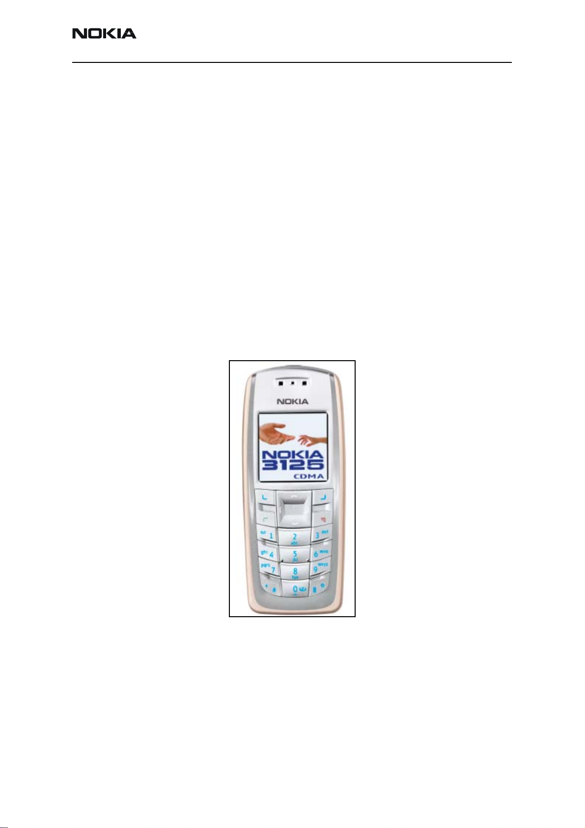
3125 (RH-61)
Series Mobile Phones
Issue 1
COMPANY CONFIDENTIAL
ISSUE 1 08/2004
Copyright © 2004 Nokia. All Rights Reserved.
Page 2

Nokia Customer Care
Amendment Record Sheet
Amendment No Date Inserted By Comments
08/2004 N. Cheshier Issue 1
ISSUE 1 08/2004 COMPANY CONFIDENTIAL 2
Copyright © 2004 Nokia. All Rights Reserved.
Page 3

Nokia Customer Care
Copyright © 2004 Nokia. All rights reserved.
Reproduction, transfer, dist ribut io n or st orage of par t o r all of t he con tents i n
this document in any form withou t the prior written permis sion of Nokia is prohibited.
Nokia, Nokia Connecting People, X and Y are trademarks or reg istered trademarks of Nokia Corporation. Other product and company names mentioned
herein may be trademarks or tradenames of their respective owners.
Nokia operates a policy of continuous development. Noki a reserves the right
to make changes and improvements t o any of the pro duct s descri bed in thi s
document without prior notice.
Under no circumstances shall Nokia be responsible for any loss of data or income or any special, inc idental, consequenti al or indirect d amages howsoever caused.
The contents of this doc ument are provided "as is". Except as required by applicable law, no warranties of any kind, either express or implied, including,
but not limited to, the implied warr anties of merchantability and fitness for a
particular purpose, ar e made in relation to the accura cy, reliability or conten ts
of this document. Nokia reserves the right to revise this document or withdraw it at any time without prior notice.
The availability of particular products may vary by region.
IMPORTANT
This document is intended for use by qualified service personne l
only.
ISSUE 1 08/2004 COMPANY CONFIDENTIAL 3
Copyright © 2004 Nokia. All Rights Reserved.
Page 4

Please refer to the product’s user guide for instructions re l ating
to operation, care and maintenance including important safety
information. Note also the following:
Warnings:
1. IF THE DEVICE CAN BE INSTALLED IN A VEHICLE, CARE
MUST BE TAKEN ON INSTALLATION IN VEHICLES FITTED
WITH ELECTRONIC ENGINE MANAGEMENT SYSTEMS AND
ANTI-SKID BRAKING SYSTEMS. UNDER CERTAIN FAULT
CONDITIONS, EMITTED RF ENERGY CAN AFFECT THEIR
OPERATION. IF NECESS ARY, CONSULT THE VE HICLE
DEALER/MANUFACTURER TO DETERMINE THE IMMUNITY
OF VEHICLE ELECTRONIC SYSTEMS TO RF ENERGY.
Nokia Customer Care
Warnings and Cautions
2. THE product MUST NOT BE OPERATED IN AREAS LIKE LY TO
CONTAIN POTENTIALLY EXPLOSIVE ATMOSPHERES EG
PETROL STATIONS (SERVICE STATIONS), BLASTING
AREAS ETC.
3. OPERATION OF ANY RADIO TRANSMITTING EQUIPMENT,
INCLUDING CELLULAR TELEPHONES, MAY INTERFERE
WITH THE FUNCTIONALITY OF INADEQUATELY PROTECTED MEDICAL DEVICES. CONSULT A PHYSICIAN OR
THE MANUFACTURER OF THE MEDICAL DEVICE IF YOU
HA VE AN Y QUESTIONS. OTHER ELECTRONIC EQU IPMENT
MAY ALSO BE SUBJEC T TO INTERFERENCE.
Cautions:
1. Servicing and alignment must be undertaken by qualified personnel only.
2. Ensure all work is carried out at an anti-static workstation and
that an anti-static wrist strap is worn.
3. Ensure solder, wire, or foreign matter does not enter the telephone as damage may result.
4. Use only approved components as specified in the parts list.
5. Ensure all components, modules screws and insulators are correctly re-fitted after s ervicing and alignmen t. Ensure all cables
and wires are repositioned correctly.
ISSUE 1 08/2004 COMPANY CONFIDENTIAL 4
Copyright © 2004 Nokia. All Rights Reserved.
Page 5

Nokia Customer Care
For your safety
QUALIFIED SERVICE
Only qualified personnel may install or repair phone equipment.
ACCESSORIES AND BATTERIES
Use only approved accessories and batteries. Do not connect incompatible
products.
CONNECTING TO OTHER DEVICES
When connecting to any other device, read its user’ s guide for detailed safety
instructions. Do not connect incompatible products.
ESD protection
Nokia requires that product ser v ice points have sufficient
ESD protection (against static electricity) when servicing
products.
Any product of which the covers are removed must be han dled with ESD protection. The SIM card can be replaced
without ESD protection if the product is otherwise ready for
use.
To replace the covers ESD protection must be applied.
All electronic parts of the product are susceptible to ESD.
Resistors, too, can be damaged by static electricity discharge.
All ESD sensitive parts must be packed in metallized protective bags during ship ping and handl ing out side any ESD
Protected Area (EPA).
Every repair action involving opening the product or handling the product components must be done under ESD
protection.
ESD protected spare part packages MUST NOT be
opened/closed out of an ESD Protected Area.
For more information and local requirements about ESD
protection and ESD Protected Area, contact your local
Nokia After Market Services representative.
ISSUE 1 08/2004 COMPANY CONFIDENTIAL 5
Copyright © 2004 Nokia. All Rights Reserved.
Page 6

Nokia Customer Care
Battery information
Note that a new battery's full performance is achieved only aft er two or three
complete charge and discharge cycles!
The battery can be charged and discharged hundreds of times but it will
eventually wear out. When th e operatin g ti me (talk- time and s tandby time) i s
noticeably shorter than normal, it is time to buy a new battery.
Use only batteries approved by the phone manufacturer and recharge the
battery only with the chargers approved by the manufacturer. Unplug the
charger when not in use. Do not leave the batte ry connected to a charger for
longer than a week, since overchargi ng may shorten its lifetime. If l eft unused
a fully charged battery will discharge itself over time.
Temperature extremes can affect the ability of your battery to charge.
For good operation times with Ni-Cd/NiMh batteries, discharge the battery
from time to time by leaving the produc t switched on unt il it t urns itsel f off (or
by using the battery discharge facility of any approved accessory available
for the product). Do not atte mpt to discharge t he batt ery by any othe r means.
Use the battery only for its intended purpose.
Never use any charger or battery which is damaged.
Do not short-circuit the ba ttery. Acc idental short-ci rcuiting can occur when a
metallic object (coin, clip or pen) ca uses direct connection of t he + and - terminals of the battery ( metal strips on the battery) fo r example when you c arry
a spare battery in your pocket or purse. Short- circuiting the terminals may
damage the battery or the connecting object.
Leaving the battery in hot or cold places, such as in a closed car in summer
or winter conditions, will reduce the capacity and lifetime of the battery. Always try to keep the battery between 15°C and 25°C (59°F and 77°F). A
phone with a hot or c old battery may temporari ly not work, even when th e battery is fully charged. Batt eries' per formance is par ticular ly limit ed in temperatures well below freezing.
Do not dispose of batteries in a fire!
Dispose of batteries according to l ocal regulations (e.g. recycling). Do not dis-
pose as household waste.
ISSUE 1 08/2004 COMPANY CONFIDENTIAL 6
Copyright © 2004 Nokia. All Rights Reserved.
Page 7

Nokia Customer Care
Care and Maintenance
The product is a product of superior design and cr aftsmanship and should be
treated with care. The suggestions belo w will help you to fulfil any warranty
obligations and to enjoy this product for many years.
Keep the phone and all its parts and accessories out of the reach of small
children.
Keep the phone dry. Precipitation, humidity and all types of liquids or moisture can contain minerals that will corrode electronic circuits.
Do not use or store the phone in dusty, dirty areas. Its moving parts can be
damaged.
Do not store the phone in hot areas. High temperatur es can shorten t he lif e
of electronic devices, damage batteries, and warp or melt certain plastics.
Do not store the phone in cold areas. When it warms up (to its normal temperature), moisture can form inside, which may damage electronic circuit
boards.
Do not drop, knock or shake the phone. Rough handling can break internal
circuit boards.
Do not use harsh chemicals, cl eaning solvents, or strong detergents to clean
the phone.
Do not paint the phone. Paint can clog the moving parts and prevent proper
operation.
Use only the supplied or an approved replacement antenna. Unauthorised
antennas, modifications or att achments could damage the phone and may violate regulations governing radio devices.
All of the above sug gestions apply equal ly to the produc t, battery, ch arger or
any accessory.
ISSUE 1 08/2004 COMPANY CONFIDENTIAL 7
Copyright © 2004 Nokia. All Rights Reserved.
Page 8

Nokia Customer Care
Company Policy
Our policy is of continuous devel opment; details of all technical modifications
will be included with service bulletins.
While every endeavour has been made to ensure the accuracy of this document, some errors may exist. If any errors are found by the reader, NOKIA
MOBILE PHONES Business Group should be notified in writing.
Please state:
Title of the Document + Issue Number/Date of publication
Latest Amendment Number (if applicabl e)
Page(s) and/or Figure(s) in error
Please se nd to :
NOKIA CORPORATION
Nokia Mobile Phones Business Group
Nokia Customer Care
PO Box 86
FIN-24101 SALO
Finland
ISSUE 1 08/2004 COMPANY CONFIDENTIAL 8
Copyright © 2004 Nokia. All Rights Reserved.
Page 9

Nokia Customer Care
Table of Contents
1- General Information
2- Parts Lists and Exploded View
3- Service So ftware Instru ctions
4- Service Tools
5- Disassembly/Reassembly Instr uctions
6- BB Description and Troubleshooting
7- RF Description and Troubleshooting
8- Schematics
ISSUE 1 08/2004 COMPANY CONFIDENTIAL 9
Copyright © 2004 Nokia. All Rights Reserved.
Page 10

Nokia Customer Care
3125 (RH-61) Series Transceivers
General Information
Issue 1 08/2004 Company Confidential ©2004 Nokia Corporation
Page 11

3125 (RH-61)
General Information
Contents Page
Introduction ..................................................................................................................................................... 3
Module List .................................................................................................................................................... 4
Technical Specifications ............................................................................................................................ 5
Supported Accessories ...............................................................................................................................5
Page 2 ©2004 Nokia Corporation Company Confidential Issue 1 08/2004
Page 12
3125 (RH-61)
Nokia Customer Care General Information
Introduction
The 3125 is an 800 MHz CDMA DCT4 transceiver and supports the CDMA IS-95 and
IS-2000 interfaces. Features include the following:
• High-resolution 4,096 color display (128 x 128)
• Keymat support for the visually impaired
• Internal antenna
• Voice tagging
• Internal vibra
• 16 polyphonic ring tones (MIDI)
• Costomizeable covers, ring tones, screensavers, etc.
• Optional, network-dependent features:
• Video and multimedia messaging
• Java and application downloading
• High-speed data (HSD)
Issue 1 08/2004 ©2004 Nokia Corporation Company Confidential Page 3
Page 13
3125 (RH-61)
General Information
Parameter Mode Value and Unit
Dimensions:
Volume
Length
Width
Thickness
Weight
74 cc
102 mm
43 mm
16-22 mm
85 g
Module List
Talk time
Standby time
Description Code
A-cover assembly:
Metallic Blue
Dune Beige
Camellia
Aluminum
Clay Red
Keypad:
Blank
Latin
BoPoMoFo
Hindi (without “i”)
Stroke (China)
Thai (Generic)
Thai (Hutch)
IS-95 up to 4.0 hours
IS-2000 up to 3.0 hours
IS-95 up to 168 hours
IS-2000 up to 312 hours
0266032
0266031
0266030
0266029
0266028
9791414
9791415
9791416
9797092
9797093
9797112
9797111
Screws 9380209
LCD assembly 0211425
PWB module 0202397
B-cover assembly:
Metallic Blue
Dune Beige
Domesheet frame assembly 9481160
Battery (BL-5C) 0670400
0264009
0264008
Page 4 ©2004 Nokia Corporation Company Confidential Issue 1 08/2004
Page 14
3125 (RH-61)
Nokia Customer Care General Information
Description Code
C-cover
Metallic Blue
Dune Beige
Camellia
Aluminum
Clay Red
9453963
9453961
9453959
9453957
9453955
Technical Specifications
Parameter Unit
Cellular system CDMA, IS2000
RX frequency band 869.04 ... 893.91 MHz
TX frequency band 824.04 ... 848.97 MHz
Output power 23 dBm
Duplex spacing 45 MHz
Number of RF channels 832
Channel spacing 30 kHz
Power levels -50 to +25.3 dBm CDMA
Method of frequency synthesis Three digital phase locked loops:
Frequency control 19.2 MHz VCTCXO: AFC used
Receiver type Linear, one IF for CDMA
Modulator type OQPSK
Supported Accessories
Type Name
AC-1 Retractable charger
VHF RX 367.2 MHz
VHF TX 457.2 MHz
UHF 1052.61 - 1077.57 MHz
ACP-7 Standard charger
ACP-12 Travel charger
AD-5B Wireless audio adapter
BHF-1 Headrest handsfree
BHF-3 Headrest handsfree
CARK-126 Car kit (for APAC)
DCV-14 Desk stand with 1-button synchronization
Issue 1 08/2004 ©2004 Nokia Corporation Company Confidential Page 5
Page 15
3125 (RH-61)
General Information
Type Name
DKU-5 USB data cable
HDA-10 TTY adapter (US)
HDB-4 Boom headset
HDW-2 Bluetooth wireless headset
HS-1C Camera headset (US)
HS-2R FM stereo headset (US)
HS-3W Wireless clip-on headset
HS-4W Wireless boom headset
HS-5 Standard earbud headset
HS-10 Retractable headset
LCH-12 Mobile charger
LPS-4 Inductive loopset
MBC-15S Mobile holder
PT-3 Fun camera (US)
SU-5 Image viewer
Page 6 ©2004 Nokia Corporation Company Confidential Issue 1 08/2004
Page 16

Nokia Customer Care
3125 (RH-61) Series Transceivers
Parts Lists and Exploded View
Issue 1 08/2004 Company Confidential ©2004 Nokia Corporation
Page 17

3125 (RH-61)
Parts Lists and Exploded View
Contents Page
Exploded View ................................................................................................................................................. 3
Assembly Parts ............................................................................................................................................. 3
Parts List............................................................................................................................................................ 5
3125 (RH-61) — Build 004 — Engine Code 0202397 ....................................................................... 5
Page 2 ©2004 Nokia Corporation Company Confidential Issue 1 08/2004
Page 18
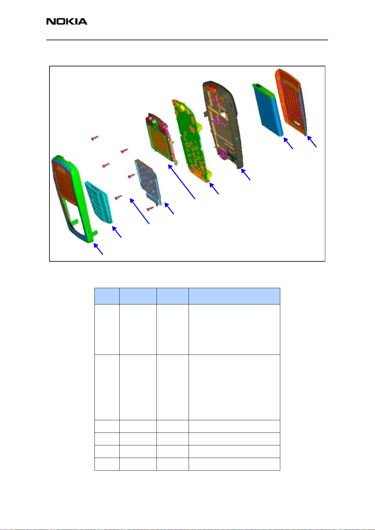
3125 (RH-61)
Nokia Customer Care Parts Lists and Exploded View
Exploded View
Assembly Parts
5
4
3
2
1
6
Item Quantity Code Description
11
0266032
0266031
0266030
0266029
0266028
A-cover assembly:
Metallic Blue
Dune Beige
Camellia
Aluminum
Clay Red
8
7
9
21
9791414
9791415
9791416
9797092
9797093
9797112
9797111
3 6 9380209 Screws 1.8X6 RF T6+BLK
4 1 9481160 Dome sheet frame assembly
5 1 0211425 LCD module assembly
6 1 0202397 PWB
Keymat assembly
Blank
Latin
BoPoMoFo
Hindi (without “i”)
Stroke (China)
Thai (Generic)
Thai (Hutch)
Issue 1 08/2004 ©2004 Nokia Corporation Company Confidential Page 3
Page 19
3125 (RH-61)
Parts Lists and Exploded View
Item Quantity Code Description
71
0264009
0264008
8 1 0670400 Battery (BL-5C)
91
9453963
9453961
9453959
9453957
9453955
1 9453272 C-cover release button
1 9510935 C-cover release spring
1 5140265 Microphone assembly
1 5400243 DC-Jack 3.5mm 3POL SPR 90DEG
1 6800057 Vibra 1.3V 80MA
1 9453374 Power button
1 0660303 Antenna assembly
1 9517328 Shield assembly
B-cover assembly:
Metallic Blue
Dune Beige
C-cover assembly:
Metallic Blue
Dune Beige
Camellia
Aluminum
Clay Red
1 9560199 SIM flap
1 9511259 LCD frame assembly
Page 4 ©2004 Nokia Corporation Company Confidential Issue 1 08/2004
Page 20
3125 (RH-61)
Nokia Customer Care Parts Lists and Exploded View
Parts List
3125 (RH-61) — Build 004 — Engine Code 0202397
Code Item Side X Y Description
1419003 R200 BOTTOM L 7 CHIPRES 0W5 0R22 J 200PPM 1210
1430121 R302 BOTTOM O 9 CHIPRES 0W06 22K F 200PPM 0402
1430191 R156 BOTTOM O 7 CHIPRES 0W06 180K F 200PPM 0402
1430681 R607 BOTTOM G 6 CHIPRES 0W06 4R3 J 0402
1430681 R608 BOTTOM E 5 CHIPRES 0W06 4R3 J 0402
1430681 R617 BOTTOM G 6 CHIPRES 0W06 4R3 J 0402
1430681 R633 BOTTOM E 5 CHIPRES 0W06 4R3 J 0402
1430690 R270 BOTTOM P 6 CHIPRES JUMPER 0R0 0402
1430690 R914 BOTTOM C 5 CHIPRES JUMPER 0R0 0402
1430691 R632 BOTTOM E 7 CHIPRES 0W06 2R2 J 0402
1430693 R167 BOTTOM N 8 CHIPRES 0W06 5R6 J 0402
1430693 R168 BOTTOM N 8 CHIPRES 0W06 5R6 J 0402
1430693 R177 BOTTOM B 6 CHIPRES 0W06 5R6 J 0402
1430693 R178 BOTTOM A 6 CHIPRES 0W06 5R6 J 0402
1430693 R606 BOTTOM G 5 CHIPRES 0W06 5R6 J 0402
1430693 R609 BOTTOM G 5 CHIPRES 0W06 5R6 J 0402
1430693 R629 BOTTOM G 6 CHIPRES 0W06 5R6 J 0402
1430693 R910 BOTTOM D 6 CHIPRES 0W06 5R6 J 0402
1430700 R502 BOTTOM H 5 CHIPRES 0W06 10R J 0402
1430700 R516 BOTTOM J 5 CHIPRES 0W06 10R J 0402
1430700 R614 BOTTOM G 5 CHIPRES 0W06 10R J 0402
1430700 R618 BOTTOM H 7 CHIPRES 0W06 10R J 0402
1430700 R620 BOTTOM G 6 CHIPRES 0W06 10R J 0402
1430700 R701 BOTTOM J 9 CHIPRES 0W06 10R J 0402
1430700 R703 BOTTOM I 10 CHIPRES 0W06 10R J 0402
1430700 R715 BOTTOM J 10 CHIPRES 0W06 10R J 0402
1430708 R911 BOTTOM C 5 CHIPRES 0W06 18R J 0402
1430714 R315 BOTTOM P 4 CHIPRES 0W06 33R J 0402
1430718 R504 BOTTOM K 5 CHIPRES 0W06 47R J 0402
Issue 1 08/2004 ©2004 Nokia Corporation Company Confidential Page 5
Page 21

3125 (RH-61)
Parts Lists and Exploded View
Code Item Side X Y Description
1430722 R301 BOTTOM R 4 CHIPRES 0W06 68R J 0402
1430722 R303 BOTTOM P 4 CHIPRES 0W06 68R J 0402
1430722 R308 BOTTOM F 8 CHIPRES 0W06 68R J 0402
1430722 R316 BOTTOM P 4 CHIPRES 0W06 68R J 0402
1430724 R905 BOTTOM C 5 CHIPRES 0W06 82R J 0402
1430726 R602 BOTTOM H 6 CHIPRES 0W06 100R J 0402
1430726 R603 BOTTOM M 7 CHIPRES 0W06 100R J 0402
1430726 R605 BOTTOM L 6 CHIPRES 0W06 100R J 0402
1430734 R309 BOTTOM F 8 CHIPRES 0W06 220R J 0402
1430734 R310 BOTTOM F 8 CHIPRES 0W06 220R J 0402
1430738 R912 BOTTOM D 5 CHIPRES 0W06 270R J 0402
1430738 R913 BOTTOM C 5 CHIPRES 0W06 270R J 0402
1430744 R154 BOTTOM N 8 CHIPRES 0W06 470R J 0402
1430754 R702 BOTTOM H 8 CHIPRES 0W06 1K0 J 0402
1430758 R616 BOTTOM F 7 CHIPRES 0W06 1K5 J 0402
1430762 R624 BOTTOM G 4 CHIPRES 0W06 2K2 J 0402
1430764 R321 BOTTOM Q 4 CHIPRES 0W06 3K3 J 0402
1430764 R427 BOTTOM M 6 CHIPRES 0W06 3K3 J 0402
1430764 R433 BOTTOM L 6 CHIPRES 0W06 3K3 J 0402
1430764 R435 BOTTOM K 4 CHIPRES 0W06 3K3 J 0402
1430764 R720 BOTTOM I 10 CHIPRES 0W06 3K3 J 0402
1430770 R306 BOTTOM B 7 CHIPRES 0W06 4K7 J 0402
1430770 R450 BOTTOM N 6 CHIPRES 0W06 4K7 J 0402
1430770 R508 BOTTOM H 4 CHIPRES 0W06 4K7 J 0402
1430770 R509 BOTTOM H 4 CHIPRES 0W06 4K7 J 0402
1430772 R157 BOTTOM O 7 CHIPRES 0W06 5K6 J 0402
1430772 R512 BOTTOM H 4 CHIPRES 0W06 5K6 J 0402
1430772 R626 BOTTOM G 5 CHIPRES 0W06 5K6 J 0402
1430772 R630 BOTTOM G 4 CHIPRES 0W06 5K6 J 0402
1430772 R631 BOTTOM G 4 CHIPRES 0W06 5K6 J 0402
1430772 R718 BOTTOM I 10 CHIPRES 0W06 5K6 J 0402
1430778 R207 BOTTOM O 10 CHIPRES 0W06 10K J 0402
Page 6 ©2004 Nokia Corporation Company Confidential Issue 1 08/2004
Page 22

3125 (RH-61)
Nokia Customer Care Parts Lists and Exploded View
Code Item Side X Y Description
1430778 R517 BOTTOM J 5 CHIPRES 0W06 10K J 0402
1430796 R155 BOTTOM O 8 CHIPRES 0W06 47K J 0402
1430796 R173 BOTTOM O 8 CHIPRES 0W06 47K J 0402
1430796 R902 BOTTOM C 7 CHIPRES 0W06 47K J 0402
1430804 R107 BOTTOM O 6 CHIPRES 0W06 100K J 0402
1430804 R109 BOTTOM R 8 CHIPRES 0W06 100K J 0402
1430806 R706 BOTTOM I 8 CHIPRES 0W06 120K J 0402
1430812 R104 BOTTOM R 7 CHIPRES 0W06 220K J 0402
1430832 R814 BOTTOM D 9 CHIPRES 0W06 2K7 J 0402
1430915 R300 BOTTOM O 9 CHIPRES 0W06 1K3 F 250PPM 0402
1620027 R100 BOTTOM R 7 RES NETWORK 0W06 2X47R J 0404
1620027 R101 BOTTOM R 8 RES NETWORK 0W06 2X47R J 0404
1620027 R102 BOTTOM R 8 RES NETWORK 0W06 2X47R J 0404
1620029 R206 BOTTOM M 10 RES NETWORK 0W06 2X4K7 J 0404
1620031 R150 TOP T 8 RES NETWORK 0W06 2X1K0 J 0404
1620031 R151 BOTTOM O 8 RES NETWORK 0W06 2X1K0 J 0404
1620031 R152 TOP T 8 RES NETWORK 0W06 2X1K0 J 0404
1620031 R170 BOTTOM R 5 RES NETWORK 0W06 2X1K0 J 0404
1620031 R171 BOTTOM Q 5 RES NETWORK 0W06 2X1K0 J 0404
1620031 R172 BOTTOM O 8 RES NETWORK 0W06 2X1K0 J 0404
1620067 R202 BOTTOM M 10 RES NETWORK 0W06 4X100K J 0804
1820039 R106 BOTTOM N 7 NTC RES 0W1 47K J B 4050+-3% 0402
1820039 R821 BOTTOM D 9 NTC RES 0W1 47K J B 4050+-3% 0402
1825031 R105 TOP T 9 VARISTOR ARRAY 2XVWM16V VC50 0405
1825031 R110 TOP T 9 VARISTOR ARRAY 2XVWM16V VC50 0405
1825031 R179 BOTTOM B 6 VARISTOR ARRAY 2XVWM16V VC50 0405
2310037 C260 BOTTOM K 7 CHIPCAP X5R 10U M 6V3 0805
2310037 C805 BOTTOM C 9 CHIPCAP X5R 10U M 6V3 0805
2312243 C505 BOTTOM I 5 CHIPCAP X5R 4U7 K 6V3 0805
2312243 C655 BOTTOM E 5 CHIPCAP X5R 4U7 K 6V3 0805
2312255 C806 BOTTOM E 10 CHIPCAP X5R 10U K 10V 1206
2312255 C808 BOTTOM E 9 CHIPCAP X5R 10U K 10V 1206
Issue 1 08/2004 ©2004 Nokia Corporation Company Confidential Page 7
Page 23
3125 (RH-61)
Parts Lists and Exploded View
Code Item Side X Y Description
2312411 C304 BOTTOM N 10 CHIPCAP X5R 1U0 M 25V 1206
2320009 C754 BOTTOM I 9 CHIPCAP NP0 10P J 50V 0402
2320110 C111 BOTTOM F 9 CHIPCAP X7R 10N K 50V 0603
2320143 C238 BOTTOM L 7 CHIPCAP X5R 220N K 6.3V 0402
2320481 C101 BOTTOM O 6 CHIPCAP X5R 1U K 6V3 0603
2320481 C102 BOTTOM O 6 CHIPCAP X5R 1U K 6V3 0603
2320481 C167 BOTTOM O 7 CHIPCAP X5R 1U K 6V3 0603
2320481 C175 BOTTOM N 7 CHIPCAP X5R 1U K 6V3 0603
2320481 C201 BOTTOM L 6 CHIPCAP X5R 1U K 6V3 0603
2320481 C203 BOTTOM N 10 CHIPCAP X5R 1U K 6V3 0603
2320481 C204 BOTTOM L 6 CHIPCAP X5R 1U K 6V3 0603
2320481 C205 BOTTOM L 6 CHIPCAP X5R 1U K 6V3 0603
2320481 C206 BOTTOM M 7 CHIPCAP X5R 1U K 6V3 0603
2320481 C207 BOTTOM M 10 CHIPCAP X5R 1U K 6V3 0603
2320481 C208 BOTTOM K 8 CHIPCAP X5R 1U K 6V3 0603
2320481 C212 BOTTOM M 6 CHIPCAP X5R 1U K 6V3 0603
2320481 C213 BOTTOM M 6 CHIPCAP X5R 1U K 6V3 0603
2320481 C214 BOTTOM N 7 CHIPCAP X5R 1U K 6V3 0603
2320481 C215 BOTTOM N 8 CHIPCAP X5R 1U K 6V3 0603
2320481 C219 BOTTOM K 7 CHIPCAP X5R 1U K 6V3 0603
2320481 C221 BOTTOM K 7 CHIPCAP X5R 1U K 6V3 0603
2320481 C222 BOTTOM K 8 CHIPCAP X5R 1U K 6V3 0603
2320481 C223 BOTTOM K 8 CHIPCAP X5R 1U K 6V3 0603
2320481 C224 BOTTOM K 8 CHIPCAP X5R 1U K 6V3 0603
2320481 C225 BOTTOM K 8 CHIPCAP X5R 1U K 6V3 0603
2320481 C226 BOTTOM K 9 CHIPCAP X5R 1U K 6V3 0603
2320481 C227 BOTTOM K 8 CHIPCAP X5R 1U K 6V3 0603
2320481 C228 BOTTOM K 9 CHIPCAP X5R 1U K 6V3 0603
2320481 C229 BOTTOM K 9 CHIPCAP X5R 1U K 6V3 0603
2320481 C231 BOTTOM K 9 CHIPCAP X5R 1U K 6V3 0603
2320481 C232 BOTTOM K 8 CHIPCAP X5R 1U K 6V3 0603
2320481 C233 BOTTOM K 7 CHIPCAP X5R 1U K 6V3 0603
Page 8 ©2004 Nokia Corporation Company Confidential Issue 1 08/2004
Page 24

3125 (RH-61)
Nokia Customer Care Parts Lists and Exploded View
Code Item Side X Y Description
2320481 C234 BOTTOM K 9 CHIPCAP X5R 1U K 6V3 0603
2320481 C235 BOTTOM N 6 CHIPCAP X5R 1U K 6V3 0603
2320481 C243 BOTTOM N 9 CHIPCAP X5R 1U K 6V3 0603
2320481 C316 BOTTOM O 9 CHIPCAP X5R 1U K 6V3 0603
2320481 C663 BOTTOM E 6 CHIPCAP X5R 1U K 6V3 0603
2320505 C270 BOTTOM Q 6 CHIPCAP X5R 4U7 K 6.3V 0603
2320505 C271 BOTTOM Q 6 CHIPCAP X5R 4U7 K 6.3V 0603
2320505 C274 BOTTOM Q 5 CHIPCAP X5R 4U7 K 6.3V 0603
2320505 C275 BOTTOM Q 5 CHIPCAP X5R 4U7 K 6.3V 0603
2320508 C811 BOTTOM D 9 CHIPCAP NP0 1P0 C 50V 0402
2320516 C619 BOTTOM F 5 CHIPCAP NP0 1P5 C 50V 0402
2320518 C903 BOTTOM D 7 CHIPCAP NP0 1P8 C 50V 0402
2320520 C614 BOTTOM F 5 CHIPCAP NP0 2P2 C 50V 0402
2320520 C623 BOTTOM F 5 CHIPCAP NP0 2P2 C 50V 0402
2320524 C907 BOTTOM D 6 CHIPCAP NP0 3P3 C 50V 0402
2320526 C702 BOTTOM J 8 CHIPCAP NP0 3P9 C 50V 0402
2320526 C707 BOTTOM J 8 CHIPCAP NP0 3P9 C 50V 0402
2320534 C912 BOTTOM C 5 CHIPCAP NP0 8P2 C 50V 0402
2320538 C617 BOTTOM G 5 CHIPCAP NP0 12P J 50V 0402
2320538 C618 BOTTOM G 5 CHIPCAP NP0 12P J 50V 0402
2320538 C711 BOTTOM H 9 CHIPCAP NP0 12P J 50V 0402
2320540 C603 BOTTOM G 7 CHIPCAP NP0 15P J 50V 0402
2320544 C103 BOTTOM R 8 CHIPCAP NP0 22P J 50V 0402
2320544 C104 BOTTOM R 8 CHIPCAP NP0 22P J 50V 0402
2320544 C105 BOTTOM R 7 CHIPCAP NP0 22P J 50V 0402
2320544 C177 BOTTOM O 7 CHIPCAP NP0 22P J 50V 0402
2320544 C630 BOTTOM E 7 CHIPCAP NP0 22P J 50V 0402
2320546 C917 BOTTOM C 6 CHIPCAP NP0 27P J 50V 0402
2320548 C506 BOTTOM I 5 CHIPCAP NP0 33P J 50V 0402
2320550 C152 BOTTOM O 8 CHIPCAP NP0 39P J 50V 0402
2320550 C156 BOTTOM N 8 CHIPCAP NP0 39P J 50V 0402
2320550 C178 BOTTOM N 8 CHIPCAP NP0 39P J 50V 0402
Issue 1 08/2004 ©2004 Nokia Corporation Company Confidential Page 9
Page 25

3125 (RH-61)
Parts Lists and Exploded View
Code Item Side X Y Description
2320550 C179 BOTTOM N 8 CHIPCAP NP0 39P J 50V 0402
2320550 C624 BOTTOM E 6 CHIPCAP NP0 39P J 50V 0402
2320552 C100 BOTTOM F 9 CHIPCAP NP0 47P J 50V 0402
2320552 C115 BOTTOM F 9 CHIPCAP NP0 47P J 50V 0402
2320552 C153 TOP T 8 CHIPCAP NP0 47P J 50V 0402
2320552 C171 BOTTOM Q 5 CHIPCAP NP0 47P J 50V 0402
2320552 C306 TOP A 7 CHIPCAP NP0 47P J 50V 0402
2320552 C309 TOP C 7 CHIPCAP NP0 47P J 50V 0402
2320552 C656 BOTTOM F 5 CHIPCAP NP0 47P J 50V 0402
2320554 C901 BOTTOM D 5 CHIPCAP NP0 56P J 50V 0402
2320560 C644 BOTTOM G 6 CHIPCAP NP0 100P J 50V 0402
2320560 C659 BOTTOM G 7 CHIPCAP NP0 100P J 50V 0402
2320560 C906 BOTTOM D 6 CHIPCAP NP0 100P J 50V 0402
2320560 C909 BOTTOM C 7 CHIPCAP NP0 100P J 50V 0402
2320564 C802 BOTTOM E 9 CHIPCAP NP0 150P J 50V 0402
2320576 C813 BOTTOM E 8 CHIPCAP X7R 470P J 50V 0402
2320584 C106 TOP T 7 CHIPCAP X7R 1N0 J 50V 0402
2320584 C510 BOTTOM J 3 CHIPCAP X7R 1N0 J 50V 0402
2320584 C511 BOTTOM H 4 CHIPCAP X7R 1N0 J 50V 0402
2320584 C522 BOTTOM J 4 CHIPCAP X7R 1N0 J 50V 0402
2320584 C600 BOTTOM G 6 CHIPCAP X7R 1N0 J 50V 0402
2320584 C605 BOTTOM G 6 CHIPCAP X7R 1N0 J 50V 0402
2320584 C606 BOTTOM F 7 CHIPCAP X7R 1N0 J 50V 0402
2320584 C611 BOTTOM E 5 CHIPCAP X7R 1N0 J 50V 0402
2320584 C612 BOTTOM E 6 CHIPCAP X7R 1N0 J 50V 0402
2320584 C633 BOTTOM G 6 CHIPCAP X7R 1N0 J 50V 0402
2320584 C635 BOTTOM G 6 CHIPCAP X7R 1N0 J 50V 0402
2320584 C638 BOTTOM G 5 CHIPCAP X7R 1N0 J 50V 0402
2320584 C643 BOTTOM F 7 CHIPCAP X7R 1N0 J 50V 0402
2320584 C658 BOTTOM G 6 CHIPCAP X7R 1N0 J 50V 0402
2320584 C706 BOTTOM J 10 CHIPCAP X7R 1N0 J 50V 0402
2320584 C712 BOTTOM J 9 CHIPCAP X7R 1N0 J 50V 0402
Page 10 ©2004 Nokia Corporation Company Confidential Issue 1 08/2004
Page 26

3125 (RH-61)
Nokia Customer Care Parts Lists and Exploded View
Code Item Side X Y Description
2320584 C735 BOTTOM H 8 CHIPCAP X7R 1N0 J 50V 0402
2320584 C736 BOTTOM H 8 CHIPCAP X7R 1N0 J 50V 0402
2320584 C814 BOTTOM D 8 CHIPCAP X7R 1N0 J 50V 0402
2320584 C919 BOTTOM C 5 CHIPCAP X7R 1N0 J 50V 0402
2320588 C516 BOTTOM H 4 CHIPCAP X7R 1N5 J 50V 0402
2320592 C164 BOTTOM O 7 CHIPCAP X7R 2N2 J 50V 0402
2320592 C646 BOTTOM G 4 CHIPCAP X7R 2N2 J 50V 0402
2320592 C647 BOTTOM F 5 CHIPCAP X7R 2N2 J 50V 0402
2320596 C601 BOTTOM F 7 CHIPCAP X7R 3N3 J 50V 0402
2320596 C913 BOTTOM C 5 CHIPCAP X7R 3N3 J 50V 0402
2320618 C519 BOTTOM H 4 CHIPCAP X7R 4N7 J 25V 0402
2320620 C713 BOTTOM J 10 CHIPCAP X7R 10N J 16V 0402
2320620 C744 BOTTOM J 9 CHIPCAP X7R 10N J 16V 0402
2320621 C641 BOTTOM F 7 USE 2320635 NP0 0P5 C 50V 0402
2320760 C728 BOTTOM I 9 CHIPCAP X7R 4N7 K 25V 0402
2320771 C648 BOTTOM G 5 CHIPCAP X5R 27N K 10V 0402
2320778 C113 BOTTOM O 7 CHIPCAP X7R 10N K 16V 0402
2320778 C202 BOTTOM K 7 CHIPCAP X7R 10N K 16V 0402
2320778 C220 BOTTOM M 10 CHIPCAP X7R 10N K 16V 0402
2320778 C240 BOTTOM M 10 CHIPCAP X7R 10N K 16V 0402
2320778 C241 BOTTOM L 10 CHIPCAP X7R 10N K 16V 0402
2320778 C310 BOTTOM B 6 CHIPCAP X7R 10N K 16V 0402
2320778 C422 BOTTOM M 6 CHIPCAP X7R 10N K 16V 0402
2320778 C426 BOTTOM L 6 CHIPCAP X7R 10N K 16V 0402
2320778 C428 BOTTOM K 4 CHIPCAP X7R 10N K 16V 0402
2320778 C450 BOTTOM O 6 CHIPCAP X7R 10N K 16V 0402
2320778 C454 BOTTOM O 6 CHIPCAP X7R 10N K 16V 0402
2320778 C650 BOTTOM H 5 CHIPCAP X7R 10N K 16V 0402
2320778 C652 BOTTOM G 5 CHIPCAP X7R 10N K 16V 0402
2320778 C703 BOTTOM I 8 CHIPCAP X7R 10N K 16V 0402
2320778 C704 BOTTOM I 9 CHIPCAP X7R 10N K 16V 0402
2320778 C810 BOTTOM D 9 CHIPCAP X7R 10N K 16V 0402
Issue 1 08/2004 ©2004 Nokia Corporation Company Confidential Page 11
Page 27

3125 (RH-61)
Parts Lists and Exploded View
Code Item Side X Y Description
2320778 C816 BOTTOM E 8 CHIPCAP X7R 10N K 16V 0402
2320783 C807 BOTTOM E 5 CHIPCAP X7R 33N K 10V 0402
2320785 C918 BOTTOM D 7 CHIPCAP X7R 47N K 10V 0402
2320787 C756 BOTTOM I 9 CHIPCAP X7R 15N K 16V 0402
2320805 C151 BOTTOM O 8 CHIPCAP X5R 100N K 10V 0402
2320805 C154 BOTTOM O 8 CHIPCAP X5R 100N K 10V 0402
2320805 C169 BOTTOM O 8 CHIPCAP X5R 100N K 10V 0402
2320805 C172 BOTTOM O 8 CHIPCAP X5R 100N K 10V 0402
2320805 C174 BOTTOM O 7 CHIPCAP X5R 100N K 10V 0402
2320805 C180 BOTTOM R 5 CHIPCAP X5R 100N K 10V 0402
2320805 C181 TOP T 8 CHIPCAP X5R 100N K 10V 0402
2320805 C218 BOTTOM L 10 CHIPCAP X5R 100N K 10V 0402
2320805 C230 BOTTOM K 8 CHIPCAP X5R 100N K 10V 0402
2320805 C236 BOTTOM K 9 CHIPCAP X5R 100N K 10V 0402
2320805 C237 BOTTOM K 9 CHIPCAP X5R 100N K 10V 0402
2320805 C239 BOTTOM L 10 CHIPCAP X5R 100N K 10V 0402
2320805 C273 BOTTOM R 6 CHIPCAP X5R 100N K 10V 0402
2320805 C300 TOP B 7 CHIPCAP X5R 100N K 10V 0402
2320805 C301 TOP C 7 CHIPCAP X5R 100N K 10V 0402
2320805 C303 BOTTOM O 8 CHIPCAP X5R 100N K 10V 0402
2320805 C400 BOTTOM M 3 CHIPCAP X5R 100N K 10V 0402
2320805 C401 BOTTOM K 6 CHIPCAP X5R 100N K 10V 0402
2320805 C402 BOTTOM M 6 CHIPCAP X5R 100N K 10V 0402
2320805 C403 BOTTOM K 5 CHIPCAP X5R 100N K 10V 0402
2320805 C404 BOTTOM N 3 CHIPCAP X5R 100N K 10V 0402
2320805 C405 BOTTOM K 5 CHIPCAP X5R 100N K 10V 0402
2320805 C451 BOTTOM P 5 CHIPCAP X5R 100N K 10V 0402
2320805 C521 BOTTOM J 4 CHIPCAP X5R 100N K 10V 0402
2320805 C636 BOTTOM F 5 CHIPCAP X5R 100N K 10V 0402
2320805 C651 BOTTOM H 6 CHIPCAP X5R 100N K 10V 0402
2320805 C654 BOTTOM G 5 CHIPCAP X5R 100N K 10V 0402
2320805 C710 BOTTOM H 9 CHIPCAP X5R 100N K 10V 0402
Page 12 ©2004 Nokia Corporation Company Confidential Issue 1 08/2004
Page 28
3125 (RH-61)
Nokia Customer Care Parts Lists and Exploded View
Code Item Side X Y Description
2320805 C720 BOTTOM J 9 CHIPCAP X5R 100N K 10V 0402
2320805 C725 BOTTOM I 8 CHIPCAP X5R 100N K 10V 0402
2320805 C730 BOTTOM I 9 CHIPCAP X5R 100N K 10V 0402
2320805 C731 BOTTOM I 8 CHIPCAP X5R 100N K 10V 0402
2320805 C734 BOTTOM H 9 CHIPCAP X5R 100N K 10V 0402
2320805 C742 BOTTOM I 8 CHIPCAP X5R 100N K 10V 0402
2320805 C757 BOTTOM H 10 CHIPCAP X5R 100N K 10V 0402
2320805 C803 BOTTOM E 5 CHIPCAP X5R 100N K 10V 0402
2320805 C914 BOTTOM C 5 CHIPCAP X5R 100N K 10V 0402
2321007 C155 BOTTOM O 7 CHIPCAP X7R 22N K 16V 0402
2321007 C166 BOTTOM O 7 CHIPCAP X7R 22N K 16V 0402
2420029 C520 BOTTOM H 5 CHIPCAP PPS 39N G 16V 1206
3203705 L100 TOP T 6 FERRITE BEAD 0.015R 42R/100M 0805
3203741 L107 TOP T 7 FERRITE BEAD 0R5 600R/100MHZ 0603
3203743 L270 BOTTOM Q 6 FERR.BEAD 0R03 42R/100MHZ 3A 0805
3203743 L301 BOTTOM O 9 FERR.BEAD 0R03 42R/100MHZ 3A 0805
3203755 L106 TOP T 7 FERRITE BEAD 0.6R 600R/100MZ 0402
3203767 L150 BOTTOM E 3 FERR.BEAD 240R/100M 0.4A 0R3 0402
3203767 L151 BOTTOM E 3 FERR.BEAD 240R/100M 0.4A 0R3 0402
3203801 L102 TOP T 8 CHIP BEAD ARRAY 2X1000R 0405
3203801 L103 TOP T 9 CHIP BEAD ARRAY 2X1000R 0405
3640119 L300 BOTTOM N 9 CHOKE 22U M 1R4 0.33A 3.3X3.3X1.5
3640133 L800 BOTTOM D 10 CHIP COIL 2U7 K Q21/1MHZ 3.0X3.4
3640165 L271 BOTTOM P 6 CHOKE 10UH M 0.49A 3.0X2.8X1.2MM
3645011 L910 BOTTOM D 5 CHIP COIL 68NH J Q12/100MHZ 0603
3645161 L909 BOTTOM C 5 CHIP COIL 150N J Q14/100MHZ 0603
3645183 L701 BOTTOM J 8 CHIP COIL 56N J Q12/100MHZ 0603
3645189 L903 BOTTOM D 6 CHIP COIL 100N J Q12/100MHZ 0603
3645363 L708 BOTTOM J 9 CHIP COIL 22N J Q40/250MHZ 0603
3645375 L600 BOTTOM G 7 CHIP COIL 12N G Q35/250MHZ 0603
3645375 L601 BOTTOM G 7 CHIP COIL 12N G Q35/250MHZ 0603
3646047 L606 BOTTOM F 5 CHIP COIL 3N3 +-0N3 Q28/800M 0402
Issue 1 08/2004 ©2004 Nokia Corporation Company Confidential Page 13
Page 29

3125 (RH-61)
Parts Lists and Exploded View
Code Item Side X Y Description
3646059 L607 BOTTOM F 7 CHIP COIL 5N6 +-0N3 Q28/800M 0402
3646059 L608 BOTTOM F 7 CHIP COIL 5N6 +-0N3 Q28/800M 0402
3646059 L609 BOTTOM F 7 CHIP COIL 5N6 +-0N3 Q28/800M 0402
3646061 L907 BOTTOM D 6 CHIP COIL 15N J Q30/800MHZ 0402
3646065 L615 BOTTOM G 5 CHIP COIL 12N J Q31/800MHZ 0402
3646065 L616 BOTTOM G 5 CHIP COIL 12N J Q31/800MHZ 0402
3646065 L901 BOTTOM C 7 CHIP COIL 12N J Q31/800MHZ 0402
3646069 L806 BOTTOM D 9 CHIP COIL 33N J Q23/800MHZ 0402
3646077 L702 BOTTOM I 6 CHIP COIL 82N J Q17/300MHZ 0402
3646081 L802 TOP B 5 CHIP COIL 68N J Q17/300MHZ 0402
3646099 L612 BOTTOM F 5 CHIP COIL 2N7 +-0N3 Q29/800M 0402
3646237 L908 BOTTOM C 6 CHIP COIL 18N J Q7/100MHZ 0402
3646425 L906 BOTTOM C 7 CHIP COIL 19N J Q25/250MHZ 0402
4110921 V701 BOTTOM I 10 CAP.DI BBY57-02W 1/4 16/4P SOD523
4110945 V601 BOTTOM G 4 CAP DIX2 BBY57-05W 4P7/17P SOT323
4113721 V100 TOP T 6 TVS DI 1PMT16AT3 16V 175W PWRMITE
4129011 R103 BOTTOM R 7 ASIP 4XESD *** PB-FREE *** BGA5
4129011 R317 BOTTOM R 9 ASIP 4XESD *** PB-FREE *** BGA5
4129031 Z300 BOTTOM K 6 ASIP KEYBOARD INTERFACE *PB-FREE*
4129071 R388 BOTTOM R 8 ASIP SIM INTERFACE ** PB-FREE **
4129091 N805 BOTTOM C 9 ASIP STPAC01F2 CDMA PWR DET BGA-8
4219935 N804 BOTTOM E 7 TRX2+4X10K PUMD3 N&P 50V SOT363
4219937 V317 BOTTOM Q 4 TRX2 UMT1/PUMT1 P40V100MA SOT363
4219937 V318 BOTTOM Q 4 TRX2 UMT1/PUMT1 P40V100MA SOT363
4219937 V319 BOTTOM Q 4 TRX2 UMT1/PUMT1 P40V100MA SOT363
4341703 N100 BOTTOM O 6 VREG LP3985ITLX-2.8 NOPB USMD5
4342303 N800 BOTTOM D 9 VREG CX20504 4.0X4.0X1.0MM
4342429 N150 BOTTOM O 7 AF AMP 0.4W LM4890/NCP2890 PBFREE
4342981 N302 BOTTOM O 9 DC/DC CONV TK65600 USMD8
4346047 N270 BOTTOM Q 6 DC/DC CONV LM2708H-1.35V/1.05V
4347043 D450 BOTTOM O 5 COMBO 128M NOR + 16M UTRAM FBGA44
4350429 G501 BOTTOM I 4 VCO 1051-1082MHZ 2.78V 10MA CDMA
Page 14 ©2004 Nokia Corporation Company Confidential Issue 1 08/2004
Page 30
3125 (RH-61)
Nokia Customer Care Parts Lists and Exploded View
Code Item Side X Y Description
4359025 N803 BOTTOM E 8 PW AMP CX77145 CDMA800 ORCA
4375161 N901 BOTTOM C 6 LNA/MIXER/DOWNCNTR ALFRED VQFN-24
4377017 D400 BOTTOM M 5 UPP8M V4.1E F761806 C027 144UBGA
4377027 D200 BOTTOM M 8 UEMK LF WDOG ENA TO21 Phoenix TFBGA168
4380003 N601 BOTTOM F 6 JEDI TX RFIC CX74050 7X7 LGA
4380005 N700 BOTTOM I 9 Yoda Dig-V1 MD I.F IC 5x5LGA
4510329 Z802 BOTTOM D 8 ISOLATOR 824-849MHZ .65DB 5X5X2
4510405 B200 BOTTOM M 7 CRYSTAL 32.768KHZ+-20PPM 12.5PF
4510435 G500 BOTTOM J 4 VCTCXO 19.2MHZ +-2PPM 2.78V 2.2MA
4511365 Z601 BOTTOM E 6 SAW FILT 836.5+-12.5MHZ/3DB 2.5X2
4511379 Z901 BOTTOM D 6 SAW FILT 881.5+-12.5MHZ/2.5 2X2.5
4511425 Z701 BOTTOM I 7 SAW FILT 183.6+-0.63MHZ 7X5X1.3
4512179 Z803 BOTTOM B 8 DUPL 824-849/869-894MHZ 5X5X1.8
4550257 L501 BOTTOM J 5 DIR.COUPLER 1066+/-14MHZ 3.2X1.6
4860343 V313 TOP L 5 LED LWL883 WHITE 71MCD?10MA 0603
4860343 V314 TOP L 8 LED LWL883 WHITE 71MCD?10MA 0603
4865391 V307 TOP O 6 LED LBL893 SMARTLED BLUE 14-28mCd @ 10mA
4865391 V308 TOP O 8 LED LBL893 SMARTLED BLUE 14-28mCd @ 10mA
4865391 V309 TOP R 6 LED LBL893 SMARTLED BLUE 14-28mCd @ 10mA
4865391 V312 TOP R 8 LED LBL893 SMARTLED BLUE 14-28mCd @ 10mA
5119029 F100 TOP T 5 SM FUSE F 1.5A 32V ROHS-FREE 0603
5200025 S302 BOTTOM A 7 SM TACT SW SIDE TRAVEL 0.2 MM
5409219 X387 BOTTOM Q 8 SM SIM CONNECTOR 6POL P2.54
5409253 X103 BOTTOM G 9 SM BATTERY CONN 3POL SPR 12V 2A
5420047 X801 TOP B 5 SM COAX CONN+SW F 50R 250V 6GHZ
5460061 X101 BOTTOM T 7 SM SYSTEM CONNECTOR 14POL
5469175 X302 TOP B 8 SM CONN 2X5F P0.5 PWB/PWB
Issue 1 08/2004 ©2004 Nokia Corporation Company Confidential Page 15
Page 31

3125 (RH-61)
Parts Lists and Exploded View Nokia Customer Care
This page intentionally left blank.
Page 16 ©2004 Nokia Corporation Company Confidential Issue 1 08/2004
Page 32

Nokia Customer Care
3125 (RH-61) Series Transceivers
Service Software Instructions
Issue 1 08/2004 Company Confidential ©2004 Nokia Corporation
Page 33

3125 (RH-61)
Service Software Instructions
Contents Page
Phoenix User’s Guide ..................................................................................................................................... 3
Introduction .................................................................................................................................................. 3
General Setup Procedure ........................................................................................................................ 3
Hardware Requirements for Using Phoenix ...................................................................................... 4
Installing Phoenix ........................................................................................................................................4
Installation Instructions.......................................................................................................................... 5
Software Support Bundles ........................................................................................................................ 5
Starting a Phoenix Session ....................................................................................................................... 5
Initial Session with Phoenix .................................................................................................................. 6
Scanning for a Product ........................................................................................................................... 7
Using Components ................................................................................................................................... 7
Using Profiles ............................................................................................................................................. 8
Uninstalling Phoenix ..................................................................................................................................8
Uninstalling a Phoenix Version ............................................................................................................. 8
Diego User’s Guide ......................................................................................................................................... 9
Introduction .................................................................................................................................................. 9
General Setup Procedure ........................................................................................................................ 9
Hardware Requirements ...................................................................................................................... 10
Installing Diego ..........................................................................................................................................10
Installing................................................................................................................................................... 10
Software Support Bundles ......................................................................................................................11
Starting a Diego Session .........................................................................................................................11
Initial Session with Diego and FLS-4S Dongle .............................................................................. 11
Scanning for a Product ........................................................................................................................ 13
Using Components ................................................................................................................................ 13
Uninstalling Diego .....................................................................................................................................14
Uninstalling a Diego Version .............................................................................................................. 14
Page 2 ©2004 Nokia Corporation Company Confidential Issue 1 08/2004
Page 34

3125 (RH-61)
Nokia Customer Care Service Software Instructions
Phoenix User’s Guide
Figure 1: Phoenix introduction screen
Introduction
This section briefly describes how to install Phoenix and includes some basic information
on how to use the program. More detailed information can be found in the Phoenix Help
files. Each feature in Phoenix has its own Help file, which can be activated while running
Phoenix. To activate a Help file while Phoenix is running, press the F1 key or the specific
feature’s Help button.
General Setup Procedure
Initial installation of Phoenix requires the complete Phoenix installation package, which
is around 30 MB. Because of its large size, Phoenix is provided on a CD rather than on a
3.5" floppy or as a download. To install Phoenix, follow the steps as outlined in the
material that comes with the CD.
Note: You MUST have a Nokia dongle installed on the computer prior to beginning the software
installation.
The Phoenix software is packaged into an executable bundle that allows you to doubleclick the executable to access the automatic installation program. Standard installation
(i.e., selecting all of the default choices) is highly recommended. You may do a custom
installation and place Phoenix into a special location on your hard drive, but this is only
recommended for experienced users.
The installation process requires that you reboot the computer after installing the
software. Phoenix is not usable until a reboot is completed. After the reboot, the Phoenix
icon appears on the desktop. Double-click this icon to start the program.
Figure 2: Phoenix desktop icon
Issue 1 08/2004 ©2004 Nokia Corporation Company Confidential Page 3
Page 35

3125 (RH-61)
Service Software Instructions
Hardware Requirements for Using Phoenix
Table 1: Minimum Hardware Requirements
Hardware Minimum Value
Processor 233 MHz
RAM1 64 MB
Disk space needed 50-100 MB
Table 2: Supported Operating System Information
Operating System Notes
Windows 98 SE only
Windows NT 4.0 No USB support
Windows 2000 Professional version
Installing Phoenix
Before installing the software, verify the following:
• The dongle is attached to the parallel port for PKD version dongles, or an FLS-4
version dongle is attached on either the parallel port or the USB port (if the
computer supports USB).
• Ensure that if the computer supports administrator rights (typically on Windows
NT and Windows 2000 installations) that access is enabled for the user
performing the Phoenix installation.
• If a previous version of Phoenix has been installed, it may be necessary to first
properly remove that program prior to installing the new version. If installation is
performed, be sure to reboot the computer prior to continuing. See the
"Uninstalling Phoenix" section for instructions on how to uninstall.
Page 4 ©2004 Nokia Corporation Company Confidential Issue 1 08/2004
Page 36
3125 (RH-61)
Nokia Customer Care Service Software Instructions
Installation Instructions
Use the following steps to install Phoenix:
1. Insert the CD into the computer.
2. Navigate to the CD-ROM drive, and double-click the Phoenix software package.
3. Follow the on-screen prompts.
4. Reboot the computer when the installation is complete.
Software Support Bundles
The Phoenix installation is auto-executable. You must obtain Software Support Bundles
to load software upgrade files to customer-specific phone models. These bundles are
created by Nokia Customer Care and made available by Nokia After Market Services
(AMS) on the Partners Web Page http://americas.partners.nokia.com. This web page is
password-controlled; if you have not registered as a user, contact Nokia Central Service
in Melbourne, Florida.
Similar to the Phoenix installation, these Software Support Bundles are InstallShield
executable packages. Double-click on the package and it will install automatically.
No rebooting of the computer is required.
Starting a Phoenix Session
When referring to Phoenix, Product is the cellular phone attached to the computer. More
specifically, it is the particular type of phone.
Connection is the type of cable used to attach the phone and the port on the computer
where it is attached. Refer to the Service Tools chapter for additional information.
The first time Phoenix is used, certain connection configurations must be made.
Subsequent uses will rely on these selections and they will not need to be made again.
Issue 1 08/2004 ©2004 Nokia Corporation Company Confidential Page 5
Page 37

3125 (RH-61)
Service Software Instructions
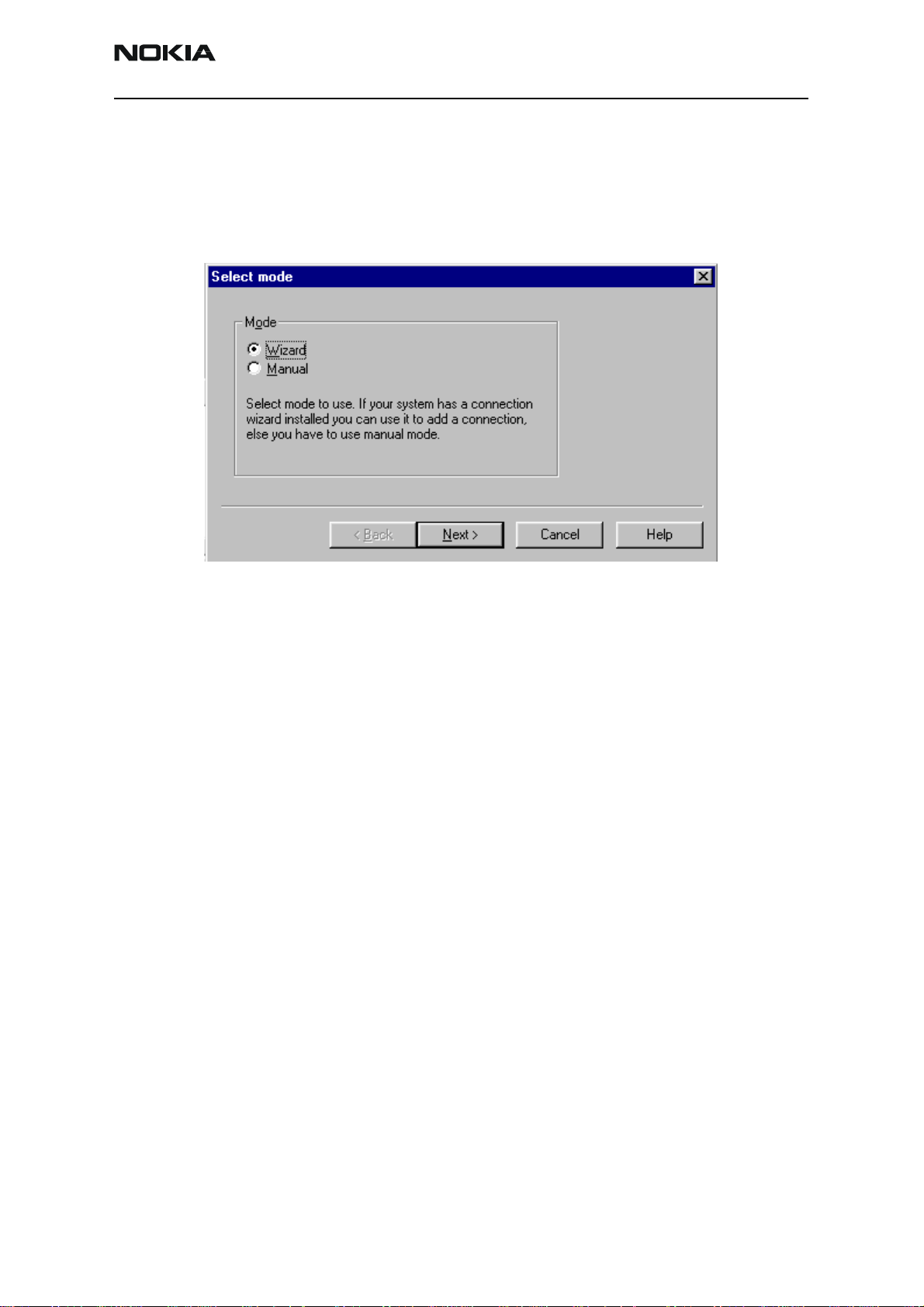
Initial Session with Phoenix
It is necessary to create a connection the first time you use Phoenix. Use the following
steps to create a connection:
1. Open the File menu, and select Manage Connections.
Figure 3: File Menu with the Manage Connections option
2. Click Add to create a new connection.
Figure 4: Manage Connections dialog box
Page 6 ©2004 Nokia Corporation Company Confidential Issue 1 08/2004
Page 38
3125 (RH-61)
Nokia Customer Care Service Software Instructions
3. Choose one of the following on the Select mode dialog box:
• Select Wizard, which allows Phoenix to auto-detect your connection
configuration.
• Select Manual, which allows you to manually select options to create the
connection.
4. Once a connection is defined, make sure that the connection you want to use
appears at the top of the list. If it does not, use the up and down arrows on the
Manage Connections dialog box to move the connection to the top, and click
Apply.
5. Close the window when you are finished.
You can now proceed with the normal initiation of a session by selecting a
product or scanning for a product.
Scanning for a Product
Many features of this program are product-specific. Therefore it is necessary to configure
Phoenix for the product on which you will be working at the beginning of the session.
Choose Scan Product from the drop-down menu list and Phoenix automatically scans
for the product and selects the necessary configurations. The status bar at the bottom
indicates if the product was found and its type.
Using Components
When working with Phoenix, tasks are generally managed by specific software
components. From the menu, select the desired component or task to be performed.
Figure 5: Select Mode dialog box
“Opening a component” is defined as opening a tool window within Phoenix. When this
window is opened, Phoenix also opens a toolbar for it and adds component-specific
menu items in the Window menu.
Issue 1 08/2004 ©2004 Nokia Corporation Company Confidential Page 7
Page 39

3125 (RH-61)
Service Software Instructions
Using Profiles
Phoenix’s Profile feature allows product, connection, and currently open components to
be stored into permanent storage by creating a profile file with a name of your choice
followed by an .nmp file extension for later retrieval.
Saved profiles makes it easy to configure Phoenix into a desired configuration with
favorite windows already opened and ready to go.
Opening and saving profiles is done via the Open Profile and Save Profile options in the
File menu.
Profiles are stored into a disk file with user-defined names. As a result, there can be
multiple profiles for different repeated tasks or user preferences.
Uninstalling Phoenix
As mentioned in the "Installing Phoenix" section, it may be necessary or desirable to
remove Phoenix. Care must be taken to follow this procedure. Failure to remove the
program properly causes misconfiguration of the computer’s registry.
Uninstalling a Phoenix Version
Use the following steps to uninstall a version of Phoenix:
1. Navigate to the computer's Control Panel, which is accessible from the Start
button or by double-clicking the “My Computer” desktop icon.
2. Double-click the “Add/Remove Programs” icon.
3. Select the Phoenix version that you want to remove, and click Add/Remove.
4. Click OK to begin the removal process.
5. Follow the on-screen instructions.
6. When the removal is complete, reboot the computer.
Page 8 ©2004 Nokia Corporation Company Confidential Issue 1 08/2004
Page 40
3125 (RH-61)
Nokia Customer Care Service Software Instructions
Diego User’s Guide
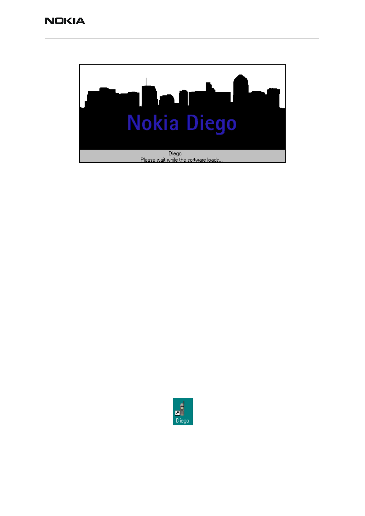
Figure 6: Diego introduction screen
Introduction
Diego was designed as an easy to use, minimal decision-making application for point of
sale locations. This section briefly describes how to install Diego and includes some basic
information about how to use the program. See the Diego Help files for more detailed
information. To activate a Help file while Diego is running, either press the F1 key or click
the specific feature's Help button.
General Setup Procedure
Initial installation of Diego requires the complete Diego installation package, which is
around 18 MB. Because of its large size, Diego is provided on a CD rather than on a 3.5"
floppy or as a download. To install Diego, follow the steps as outlined in the material that
comes with the CD.
Note: You MUST have a Nokia dongle installed on the computer prior to beginning the software
installation.
The Diego software is packaged into an executable bundle that allows you to doubleclick the executable to access the automatic installation program. Standard installation
(i.e., selecting all of the default choices) is highly recommended. You may do a custom
installation and place Diego into a special location on your hard drive, but this is only
recommended for experienced users.
The installation process requires that you reboot the computer after installing the
software. Diego is not usable until a reboot is completed. After the reboot, the Diego icon
appears on the desktop. Double-click this Icon to start the program.
Figure 7: Diego desktop icon
Issue 1 08/2004 ©2004 Nokia Corporation Company Confidential Page 9
Page 41
3125 (RH-61)
Service Software Instructions
Hardware Requirements
Table 3: Minimum Hardware Requirements
Hardware Minimum Value
Processor 233 MHz
RAM1 64 MB
Disk space needed 50-100 MB
Table 4: Supported Operating System Information
Operating System Notes
Windows 98 SE only
Windows NT 4.0 No USB support
Windows 2000 Professional version
Installing Diego
Be sure to check the following items before installing Diego:
• An FLS-4 version dongle is attached to either the parallel port or the USB port
(if the computer supports USB). An FLS-2D may be used; however, the FLS-2D
does not support the new generation DCT-4 version phones.
• If the computer supports administrator rights (typically on NT and Windows 2000
installations), ensure that access is enabled for the user performing the
installation.
• If a previous version of Diego has been installed, remove that program prior to
installing the new version. Once removal is performed, be sure to reboot the
computer prior to continuing. (See the "Uninstalling Diego" section for
instructions on how to uninstall.)
Installing
Use the following steps to install Diego:
1. Insert the CD into the computer.
2. Navigate to the CD-ROM drive, and double-click the Diego software package.
3. Follow the on-screen prompts.
4. Reboot the computer when the installation is complete.
Page 10 ©2004 Nokia Corporation Company Confidential Issue 1 08/2004
Page 42

3125 (RH-61)
Nokia Customer Care Service Software Instructions
Software Support Bundles
The Diego installation program is a generic software load. In order to support specific
custom transceivers (customer-specific phone models), it is necessary to also obtain
Software Support Bundles. These bundles are created by Nokia Customer Care and made
available by Nokia After Market Services (AMS) for the Americas region on the Partners
Web Page (http://americas.partners.nokia.com). This Web page is password-controlled.
Contact Nokia Central Service in Melbourne, Florida, if you have not registered as a user.
Similar to the Diego installation, these bundles are executables. Double-click the
executable file to automatically install the bundle. No re-booting of the computer is
necessary.
Starting a Diego Session
When referring to Diego, product is the cellular phone attached to the computer. More
specifically, product refers to the particular type of phone.
Connection is the type of cable used to attach the phone to the computer, and also
includes the port to which the cable is attached.
The first time Diego is used, certain connection configurations must be made.
Subsequent uses rely on these selections and do not need to be made again.
Initial Session with Diego and FLS-4S Dongle
You must configure the Virtual Port Connection in Diego the first time Diego is launched.
The FLS-4 dongle uses virtual port, which eliminates the need to use the serial port (as
the FLS-2D does). During the installation of the FLS-4 drivers (included in the Diego
installation package), a virtual COM port is set to the next available COM port number.
This port selection must be put into the Diego configuration.
Issue 1 08/2004 ©2004 Nokia Corporation Company Confidential Page 11
Page 43

3125 (RH-61)
Service Software Instructions
Use the following steps to select a port:
1. Select “My Computer” desktop icon, and click the “FLS Virtual Port” icon.
Figure 8: The FLS Virtual Port icon
2. Make note of the value in the Virtual Port Assignment field (COM 2 in this
example).
3. Click Add to create a new connection.
Figure 9: diego - Phone Settings dialog box
Note: COM port settings can only be entered or changed if the auto-connection feature of
Diego is disabled (as indicated in the grey Status box). To disable the auto-connect feature,
click on this icon in the toolbar.
Page 12 ©2004 Nokia Corporation Company Confidential Issue 1 08/2004
Page 44

3125 (RH-61)
Nokia Customer Care Service Software Instructions
4. Select the Virtual COM port setting.
5. Click Apply.
6. Proceed with the normal initiation of a session.
Scanning for a Product
Many features of this program are product specific. Therefore, it is necessary to
configure Diego at the beginning of the session for the product on which you will be
working.
Scanning of the product can be done manually or automatically. The default setting is
automatic scanning. In automatic scan mode, Diego automatically scans for a product at
a periodic rate. The default rate is every 5 seconds, but you can change to a different
frequency in the setup menu.
You can change the scan setting to manual scanning on the General tab on the Settings
dialog box. To manually scan for a product, click the “Connect” icon.
Using Components
When working with Diego, tasks are generally managed by specific software
components. Select the desired component or "task" to be performed from the icons
displayed in the pane on the left side of the window.
Figure 10: Serial Port tab on the Settings dialog box
Opening a component refers to opening a tool window within Diego. When this window
is opened, Diego also opens a task box, which includes component-specific menu items.
Issue 1 08/2004 ©2004 Nokia Corporation Company Confidential Page 13
Page 45

3125 (RH-61)
Service Software Instructions
Uninstalling Diego
As mentioned in the "Installing Diego" section, it may be necessary to remove a previous
version of Diego. Follow the uninstall procedure with care.
Note: Failure to remove the program properly causes a misconfiguration of the computer's registry.
Uninstalling a Diego Version
Use the following steps to uninstall a previous version of Diego:
1. Navigate to the computer's Control Panel, which is accessible from the Start
button or by double-clicking the “My Computer” desktop icon.
2. Double-click the “Add/Remove Programs” icon.
3. Select the Diego version that you want to remove, and click Add/Remove.
4. Click OK to begin the removal process.
5. Follow the on-screen instructions.
6. When the removal is complete, reboot the computer.
Page 14 ©2004 Nokia Corporation Company Confidential Issue 1 08/2004
Page 46

Nokia Customer Care
3125 (RH-61) Series Transceivers
Service Tools
Issue 1 08/2004 Company Confidential ©2004 Nokia Corporation
Page 47

3125 (RH-61)
Service Tools
Contents Page
Model 3125 Service Tools ............................................................................................................................ 3
Flashing, Testing, and Tuning ................................................................................................................... 7
High-volume Flashing and EM Calibration ....................................................................................... 7
Covers-Off Troubleshooting Using Service Jig (MJ-23)................................................................. 8
Automated Tuning and Alignment....................................................................................................... 9
Page 2 ©2004 Nokia Corporation Company Confidential Issue 1 08/2004
Page 48

3125 (RH-61)
Nokia Customer Care Service Tools
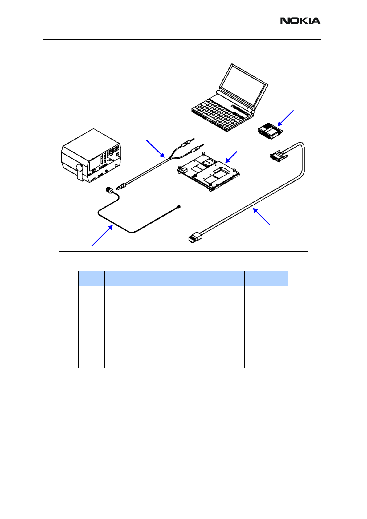
Model 3125 Service Tools
JBV-1 Docking Station MJF-17 Docking Station Adapter
0770298 0774282
The JBV-1 docking station connects flash prommers
and works in conjunction with the MJF-17 for flashing,
testing, an dan EM calibration. The docking station can
be powered by the FPS-8 or an external power supply.
Note: You must update your JBV-1s to the latest
firmware to properly operate Lynx handsets.
Note: Use the PCS-1 DC power and XRS-4 cables when
using the FPS-8 prommer box.
The MJF-17 works in conjunction with the JBV-1 docking station and the FPS-8 prommer to enable tuning,
testing, and flashing. The docking station adapter supports the LYNX batter interface, which does not require
BTEMP, and also has a built-in R-UIM card reader.
FPS-8 Flash Prommer RJ-32 Rework Jig
0080321 0770757
The FPS-8 flash prommer is used for high-volume
flashing at authorized service centers.
Note: You must register the FPS-8 in order to activate it.
(See the sales package for registration information.)
The rework jig is a PWB component that allows
de-soldering and soldering.
Issue 1 08/2004 ©2004 Nokia Corporation Company Confidential Page 3
Page 49
3125 (RH-61)
Service Tools
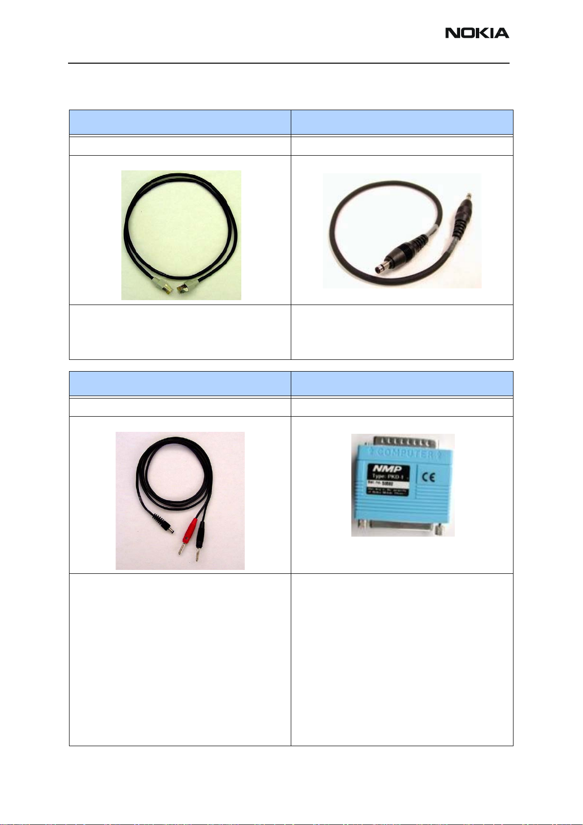
XCS-4 Mbus/Fbus Cable CA-5S DC Service Cable
0730178 0730283
The XCS-4 Service Cable is a general purpose cable for
flashing and communicating with the phone. This is
used to connect the FPS-8 box to the docking station
adapter or the service jig.
CA-5S is used for EM calibration with the JBV-1. This
cable replaces the SCB-3 DC Cable (0730114).
Note: Required by the MJF-28 Docking Station Adapter.
PCS-1 Power Cable PKD-1 SW Security Device
0730012 0750018
The Power Cable PCS-1 is used to connect the service
tools (JBV-1, MJS-82) to an external power supply.
SW security device (PKD-1) is a hardware device that,
when connected to the parallel (LPT) port of the PC,
enables the use of service software. It is not possible to
use the service software without the dongle. Printers
or other peripheral devices can be connected to the PC
through the dongle, if needed.
Caution: Make sure that you have switched off the PC
and the printer before making connections. Also, do not
connect the PKD-1 to the serial port. You may damage
your PKD-1.
Note: PKD-1RD dongles are restricted to Nokai Product
Creation Centers only.
Page 4 ©2004 Nokia Corporation Company Confidential Issue 1 08/2004
Page 50

3125 (RH-61)
Nokia Customer Care Service Tools
FLS-4S POS Flash Adapter DAU-9T MBUS Data Cable
0080543 0730267
The Point of Sale (POS) flash is a low-cost software
upgrade tool. (This requires the XCS-1 cable [0730218],
NOT included.)
FBUS cable DAU-9T provides a connection from the
serial port of the computer to the system connector of
the phone. This cable is used for diagnostic purposes.
Note: This cable does not support M-BUS.
DAU-9S (MBUS) Cable CA-25RS RF Test Cable
0730108 0730316
This is a general-purpose cable to support F / MBUS
communication between a Mod-10 device and a PC.
This cable is used for diagnostic purposes.
The CA-25RS test cable is used for CDMA RF engine
testing and tuning. This cable snaps directly on the
phone’s RF connector and converts the output to an
SMA connector. Removal of the A-cover is required.
Issue 1 08/2004 ©2004 Nokia Corporation Company Confidential Page 5
Page 51

3125 (RH-61)
Service Tools
CA-22DS Service Cable MJ-23 Module Test Jig
0730311 0770650
This cable is used for bottom connector flashing using
FLS-4S or FLC-20.
The MJ-23 secures and allows easy access to critical
areas of the handset’s PWB during troubleshooting. It
supports regulated and unregulated DC input voltages,
Local and Normal mode operations, a R-UIM card
reader, and a second DC input for VCHAR used in EM
tuning. The Jig also supports simultaneous RF connections to the CDMA engine. A completely functional UI
module is also provided on the right side.
Note: The MJ-23 is for use with the CA25RS RF cable.
SS-13 Tuning Docking Station (CDMA) XRS-6 RF Cable
0080852 0730231
SS-13 is used with the MJF-x/DA-x flashing adapters
(shown with MJF-17).
The XRS-6 cable is used to connect service tools to RF
measuring equipment.
Page 6 ©2004 Nokia Corporation Company Confidential Issue 1 08/2004
Page 52
3125 (RH-61)
Nokia Customer Care Service Tools
Flashing, Testing, and Tuning
Tightened performance specifications require more precise equipment and methods for
testing and alignment. Manual tuning can not provide accurate results for the 3125,
which means that this test has to be automated.
These setups are intended to be with the Phoenix Service Software. Both manual testing
and automated tuning are permitted with Phoenix Service Software.
High-volume Flashing and EM Calibration
5
1
3
2
Item Name Type Code
1 Flash prommer box (sales pack)
Included in FPS-8 sales pack:
Service cable
Serial cable
Power supply
2 Docking station JBV-1 0770298
3 Docking adapter MJF-17 0774282
4 DC power cable PCS-1 0730012
5 Modular cable XCS-4 0730178
Software protection key (not shown) PKD-1 0750018
FPS-8
CA-10DS
AXS-4
ACF-8
0080321
0730298
0730090
0680032
4
Service software CDMA Phoenix 8407840
Issue 1 08/2004 ©2004 Nokia Corporation Company Confidential Page 7
Page 53
3125 (RH-61)
Service Tools
Covers-Off Troubleshooting Using Service Jig (MJ-23)
2
5
1
3
Item Name Type Code
1 Module repair jig
includes RF test cable
2 DC power cable PCS-1 0730012
3 RF test cable XRS-6 0730231
4 Service MBUS/FBUS cable DAU-9S 0730108
5 Software protection key PKD-1 0750018
Service software (not shown) Phoenix 8407840
MJ-23
CA-25RS
0770650
0730316
4
Page 8 ©2004 Nokia Corporation Company Confidential Issue 1 08/2004
Page 54
3125 (RH-61)
Nokia Customer Care Service Tools
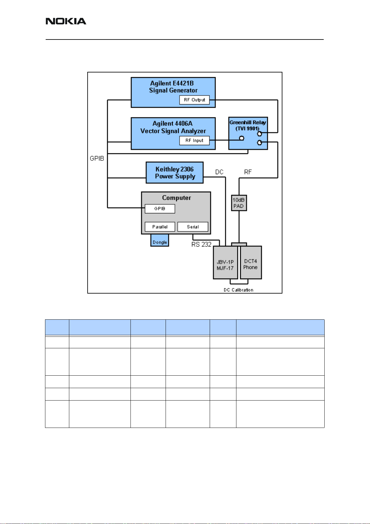
Automated Tuning and Alignment
This setup is used for tuning of the handset at Nokia Authorized Service Centers.
2
1
6
4
3
5
7
Following is the automated tuning and alignment equipment list.
Item Name MFR Model # QTY Comment
1 Vector Signal Analyzer Agilent E4406A 1
2 Signal Generator Agilent E4421B 1 Digital signal generator with
high-stability oscillator and
high-spectral purity
3 RF Series GreenHill TVi9901 1
4 Power Supply Keithly K2306 2 Programmable with sense wire
5 Win2000 PC Dell with Pentium III or above,
network card, 256M RAM, 20GB
HD, CD-ROM, etc.
Issue 1 08/2004 ©2004 Nokia Corporation Company Confidential Page 9
Page 55
3125 (RH-61)
Service Tools
Item Name MFR Model # QTY Comment
6 NI-GPIB Interface NI GPIB-USB-A 2 USB to GPIB adapter
(184983G-01)
7 Docking Station Nokia JBV-1P 1 For RF tuning, a modified JBV-1P
is used. The JBV-1P only supplies
power with sense lines to compensate voltage loss.
Page 10 ©2004 Nokia Corporation Company Confidential Issue 1 08/2004
Page 56

Nokia Customer Care
3125 (RH-61) Series Transceivers
Disassembly/Reassembly
Instructions
Issue 1 08/2004 Company Confidential ©2004 Nokia Corporation
Page 57

3125 (RH-61)
Disassembly/Reassembly Instructions Nokia Customer Care
Introduction
Use the following procedures to disassemble and reassemble the phone.
Reassembly
To reassemble the phone, complete the following disassembly procedures in reverse
order.
Disassembly
1. Press the release button before removing the C-cover.
2. Remove the A-cover.
3. Always protect the window with a protection film to avoid dust and scratches.
4. Unscrew the six T6 screws using the order shown. For assembly, you must use
Page 2 ©2004 Nokia Corporation Company Confidential Issue 1 08/2004
Page 58

3125 (RH-61)
Nokia Customer Care Disassembly/Reassembly Instructions
the reverse order and a Torx T6 PLUS with torque of 20Ncm.
Torque 20Ncm
for assembly
5. Separate the module from the B-cover and unplug the display connector
carefully by removing the UI shield from system module.
6. Separate the UI shield from the system module carefully. The key dome is
attached with adhesive tape, which must not be touched.
7. Separate the LCD from the UI shield by pressing out the LCD using a clean cloth.
Prevent the key dome tape from getting dirty.
8. Always protect the LCD window with a protection foil to avoid dust and
Issue 1 08/2004 ©2004 Nokia Corporation Company Confidential Page 3
Page 59
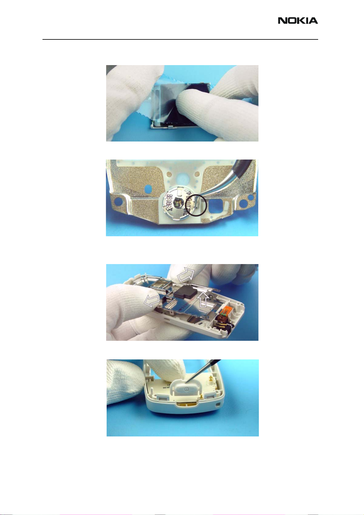
3125 (RH-61)
Disassembly/Reassembly Instructions Nokia Customer Care
scratches.
9. Remove the earpiece. Note the guiding pin when re-assembling.
10. The shielding is attached with hooks at its backside. To remove the shielding from
the B-cover, first expand the B-cover, then push the shielding upwards.
11. Remove the power button key.
Page 4 ©2004 Nokia Corporation Company Confidential Issue 1 08/2004
Page 60

3125 (RH-61)
Nokia Customer Care Disassembly/Reassembly Instructions
12. Use the SRT-6 to lift up the antenna.
13. Remove the antenna.
14. Use tweezers to remove the vibra motor.
15. Use tweezers to pull up the microphone.
16. To remove the DC jack, place tweezers between the spring contacts and under
Issue 1 08/2004 ©2004 Nokia Corporation Company Confidential Page 5
Page 61

3125 (RH-61)
Disassembly/Reassembly Instructions Nokia Customer Care
the jack. You need to use additional force to pull the jack upwards.
17. Use a flathead screwdriver as a lever to remove the release spring.
18. Turn the B-cover as shown to allow the release button to fall out.
19. Open the SIM flap and turn it as shown in the picture.
Page 6 ©2004 Nokia Corporation Company Confidential Issue 1 08/2004
Page 62

3125 (RH-61)
Nokia Customer Care Disassembly/Reassembly Instructions
20. Expand the B-cover carefully and remove the SIM flap.
Exchange of Battery Connector X103
These are the two soldered support angles.
1. Use a side cutter to cut the support angles.
2. Push tweezers into the outside openings of the battery connector and lift up the
plastic cover.
Issue 1 08/2004 ©2004 Nokia Corporation Company Confidential Page 7
Page 63
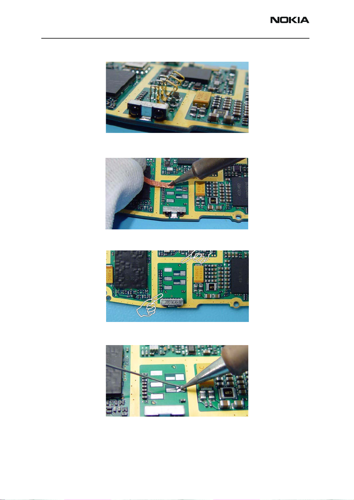
3125 (RH-61)
Disassembly/Reassembly Instructions Nokia Customer Care
3. Desolder all pins and clean the pads.
You need a soldering iron with a higher temperature when cleaning or soldering
the ground pad.
Note the location markings to fit the connector precisely.
4. Tin one of the pads to fix the connector before soldering the following pins.
5. Place the connector between the markings and solder the first support angle. If
Page 8 ©2004 Nokia Corporation Company Confidential Issue 1 08/2004
Page 64

3125 (RH-61)
Nokia Customer Care Disassembly/Reassembly Instructions
the position is exact, solder the other pins.
Issue 1 08/2004 ©2004 Nokia Corporation Company Confidential Page 9
Page 65

3125 (RH-61)
Disassembly/Reassembly Instructions Nokia Customer Care
Page 10 ©2004 Nokia Corporation Company Confidential Issue 1 08/2004
Page 66

Nokia Customer Care
3125 (RH-61) Series Transceivers
Antenna Description and
Troubleshooting
Issue 1 08/2004 Company Confidential ©2004 Nokia Corporation
Page 67

3125 (RH-61)
Antenna Description and Troubleshooting Nokia Customer Care
Contents Page
Introduction ..................................................................................................................................................... 3
Internal Antenna Missing ..........................................................................................................................3
Damaged RF Feed Pin or Ground Pin .....................................................................................................4
Wrong Internal Antenna Installed .......................................................................................................... 4
Obstructed RF Feed or Ground Pads for Internal Antenna, or IHF Speaker Pads ...................... 5
Grounding of Display Frame ..................................................................................................................... 6
Grounding of RUIM Card Flap .................................................................................................................. 7
RF Connector Failure .................................................................................................................................. 7
Page 2 ©2004 Nokia Corporation Company Confidential Issue 1 08/2004
Page 68

3125 (RH-61)
Nokia Customer Care Antenna Description and Troubleshooting
Introduction
This troubleshooting guide addresses potential failures that can affect antenna
performance of the 3125 phone, and discusses methods for correction of these failures.
Internal Antenna Missing
IHF speaker
pins
If no internal antenna is installed, the antenna gain will degrade by more than 25 dB.
Figure 1: Front view of the 3125
RF feed
Figure 2: 3125 chassis assembly
Ground pin
RF shield
• If the internal antenna is missing, install a new one.
• If the radiator looks obviously damaged, replace the internal antenna.
Issue 1 08/2004 ©2004 Nokia Corporation Company Confidential Page 3
Page 69

3125 (RH-61)
Antenna Description and Troubleshooting Nokia Customer Care
Damaged RF Feed Pin or Ground Pin
RF pin Ground pin
Spacer
IHF speaker
pins
Figure 3: Bottom (left) and top (right) views of the 3125 internal antenna
If the RF feed does not touch the PWB, then the antenna gain will degrade by more than
25dB. If the ground pin does not touch the PWB, then the antenna gain may degrade
from 5—10 dB.
Replace the internal antenna if any of the following situations apply:
IHF speaker
port
Ground pin RF pin
Radiator
• Either the RF feed pin or ground pin are broken or bent such that either pin will
not touch the PWB
• The springs for the RF or ground pin appear damaged
• The slot in the radiator has a significantly different shape
• Obvious damage to the radiator (e.g., dents, corrosion)
• The pin is stuck or has excessive friction in the plastic tube/guiding feature
resulting in the spring not working properly
• Either of the IHF speaker pins is damaged or if the IHF speaker is not functioning
Wrong Internal Antenna Installed
Figure 4: Top views of the 3100 (RH-19) (left) and 3125 (RH-61) (right) antennas
The 3100 and 3125 antennas are similar in appearance. The important visual difference
in the antennas is the slot pattern. Also, the 3125 antenna is thicker than the 3100
antenna and has a spacer on its back side.
• If the wrong antenna is installed, install the correct one.
Page 4 ©2004 Nokia Corporation Company Confidential Issue 1 08/2004
Page 70

3125 (RH-61)
Nokia Customer Care Antenna Description and Troubleshooting
Figure 5: Bottom views of the 3100 (RH-19) (left) and 3125 (RH-61) (right) antennas
Obstructed RF Feed or Ground Pads for Internal Antenna, or IHF Speaker Pads
Pad for ground pin Pad for RF pin
IHF speaker pads
Figure 6: PWB layout of RF feed and ground pads and IHF speaker pads
If the RF feed pad is obstructed, removed, or covered, the RF feed pin will not touch the
PWB and the antenna gain will degrade by more than 25 dB. If the ground pad is
obstructed, removed, or covered, the ground pin will not touch the PWB and the antenna
gain may degrade by about 5—10 dB.
• If corrosion is present or the pad is missing, replace the PWB and the phone.
• If either pad is obstructed or covered, clear or clean the pad.
If the Internal Hands Free (IHF) speaker pads are obstructed, removed, or covered, the IHF
speaker will not produce sound.
• If corrosion is present or the pad is missing, replace the PWB and the phone.
• If either pad is obstructed or covered, clear or clean the pad.
Issue 1 08/2004 ©2004 Nokia Corporation Company Confidential Page 5
Page 71

3125 (RH-61)
Antenna Description and Troubleshooting Nokia Customer Care
Grounding of Display Frame
Ungrounded screw
Grounded screw
RF connector
Grounded screw
Figure 7: Display assembly
Ungrounded screw
Note that the display frame is grounded to the PWB through the two top screws. The
grounding of the display frame impacts the radiation performance of the phone.
• If the screws are loose, then tighten them.
• If the screw bosses are stripped, replace the chassis.
• If the screws are missing, install new ones.
The middle screws should not touch the metal in the LCD frame, the metal shield over
the keypad, the PWB, or the RF shield. When driving in these screws, be sure to drive
them in straight. If the screws are driven in at an angle, it is much more likely that the
screws will touch the PWB or the RF shield. If the screws touch, the antenna
performance could change by about 1dB.
Page 6 ©2004 Nokia Corporation Company Confidential Issue 1 08/2004
Page 72

3125 (RH-61)
Nokia Customer Care Antenna Description and Troubleshooting
Grounding of RUIM Card Flap
RF shield
Conductive sticker
RUIM card flap
Figure 8: Conductive sticker grounding RUIM card flap to RF shield
The RUIM card flap needs to be grounded to the RF shield with a conductive sticker. The
shape and location of the conductive sticker is shown in Figure 8. If the sticker is
damaged or missing, then the radiated sensitivity could be reduced by 4—8 dB.
• If the conductive sticker is missing or ripped, replace the sticker.
RF Connector Failure
The RF connector could fail by not connecting the RF input to the RF output of the RF
connector. If this happens, then the antenna gain will degrade by about 25 dB. Check for
this by testing for DC conductivity between the RF input and RF output of the RF
connector. Note the DC conductivity test must be done without any cable attached to
the RF connector. Because the RF connector is also a switch, the RF output will be
disconnected from the RF input when a cable is inserted into the RF connector. When a
cable is inserted, the RF input is connected to the RF connector.
• RF input — connector to duplexer
• RF output — connects to antenna pad through vias
• RF connector — connects to coaxial cable
If the RF input is not connected properly to the RF output, replace the RF connector.
Issue 1 08/2004 ©2004 Nokia Corporation Company Confidential Page 7
Page 73

3125 (RH-61)
Antenna Description and Troubleshooting Nokia Customer Care
This page intentionally left blank.
Page 8 ©2004 Nokia Corporation Company Confidential Issue 1 08/2004
Page 74

Nokia Customer Care
3125 (RH-61) Series Transceivers
BB Description and
Troubleshooting
Issue 1 08/2004 Company Confidential ©2004 Nokia Corporation
Page 75

3125 (RH-61)
BB Description and Troubleshooting
Contents Page
Baseband Overview ........................................................................................................................................ 3
Baseband and RF Architecture ................................................................................................................ 4
Power Up and Reset ....................................................................................................................................4
Power Up - Power Key............................................................................................................................. 7
Power Up - Charger ................................................................................................................................. 7
Power Up - RTC Alarm............................................................................................................................. 8
Power Off ....................................................................................................................................................... 8
Power Consumption and Operation Modes ......................................................................................... 8
Power Distribution ...................................................................................................................................... 9
Clock Distribution ......................................................................................................................................11
RFClk (19.2 MHz Analog)..................................................................................................................... 11
RFConvClk (19.2 MHz digital) ............................................................................................................ 13
CBUSClk Interface ................................................................................................................................. 14
DBUS Clk Interface ................................................................................................................................ 14
SleepCLK (Digital) .................................................................................................................................. 15
SleepCLK (Analog).................................................................................................................................. 16
Flash Programming ...................................................................................................................................16
Connections to Baseband.................................................................................................................... 16
Baseband Power Up .............................................................................................................................. 16
Flash Programming Indication ........................................................................................................... 16
Flashing..................................................................................................................................................... 17
Flash Programming Error Codes ........................................................................................................ 19
Charging Operation ...................................................................................................................................21
Battery ...................................................................................................................................................... 21
Charging Circuitry ................................................................................................................................. 21
Charger Detection.................................................................................................................................. 22
Charge Control ....................................................................................................................................... 22
Audio .............................................................................................................................................................23
Display and Keyboard ...............................................................................................................................23
Accessories ..................................................................................................................................................24
Charging ................................................................................................................................................... 25
Pop-Port Headset Detection............................................................................................................... 26
FBus Detection........................................................................................................................................ 27
Accessory Detection Through ACI..................................................................................................... 27
SIM CAR .......................................................................................................................................................29
Test Points ...................................................................................................................................................30
Troubleshooting .........................................................................................................................................33
Top Troubleshooting Map ........................................................................................................................34
Phone is Totally Dead ........................................................................................................................... 36
Flash Programming Does Not Work ................................................................................................. 37
Power Does Not Stay on or the Phone is Jammed ....................................................................... 39
Charger ..................................................................................................................................................... 41
Audio Faults............................................................................................................................................. 42
Display Faults.......................................................................................................................................... 46
Keypad Faults.......................................................................................................................................... 48
Page 2 ©2004 Nokia Corporation Company Confidential Issue 1 08/2004
Page 76

3125 (RH-61)
Nokia Customer Care BB Description and Troubleshooting
Baseband Overview
The baseband module of the 3125 transceiver is a CDMA single-band engine.
The cellular baseband consists of three ASICs: Universal Energy Management (UEM),
Universal Phone Processor (UPP), and a 128/16 megabit combo FLASH.
The baseband architecture supports a power-saving function called sleep mode. This
sleep mode shuts off the VCTCXO, which is used as system clock source for both RF and
baseband. During the sleep mode, the system runs from a 32 kHz crystal and all the RF
regulators (VR1A, VR1B, VR2, … VR7) are off. The sleep time is determined by network
parameters. Sleep mode is entered when both the MCU and the DSP are in standby mode
and the normal VCTCXO clock is switched off. The phone is waken up by a timer running
from this 32 kHz clock supply. The period of the sleep/wake up cycle (slotted cycle) is
1.28N seconds, where N= 0, 1, 2, depending on the slot cycle index.
The 3125 supports standard Nokia 2-wire and 3-wire chargers (ACP-x and LCH-x).
However, the 3-wire chargers are treated as 2-wire chargers. The PWM control signal for
controlling the 3-wire charger is ignored. The UEM ASIC and the EM SW control
charging.
A BL-5C Li-ion battery is used as main power source, which has nominal capacity
of 850 mAh.
Issue 1 08/2004 ©2004 Nokia Corporation Company Confidential Page 3
Page 77

3125 (RH-61)
BB Description and Troubleshooting
Baseband and RF Architecture
Charger
Bottom
Conn.
Sleep Clk
32 KHz
Audio
MBus
FBusRx
FBusT
x
SIM Reader
UEM
VR1A
VR1B
VR2
VR3
VR4
VR5
VR6
VR7
VBatt
Battery
VIO
VANA
V SIM
Vflash1
Vflash2
JTAG
DC/DC
VPPPRODTP
CBus
u
B
D
MBus
FBus
GenIO
Control
s
Flash
C
ExtBus
UPP
Core
VCTCXO
19.2 MHz
Front
End
Alfred
Power Up and Reset
Power up and reset are controlled by the UEM ASIC. The baseband can be powered up in
the following ways:
RF
System
Connector
V Bat
Bus
UHF
SYNTH
Yoda
PA
VBatt
Figure 1: 3125 power distribution diagram
V Bat
LCD/Key
Jedi
• Pressing the Power button, which means grounding the PWRONX pin of the UEM
• Connecting the charger to the charger input
• Initiating the RTC Alarm, when the RTC logic has been programmed to give an
alarm
Page 4 ©2004 Nokia Corporation Company Confidential Issue 1 08/2004
Page 78

3125 (RH-61)
Nokia Customer Care BB Description and Troubleshooting
After receiving one of the above signals, the UEM counts a 20 ms delay and then enters
reset mode. The watchdog starts, and if the battery voltage is greater than Vcoff+, a
200 ms delay is started to allow references (etc.) to settle. After this delay elapses, the
VFLASH1 regulator is enabled. Then, 500 us later, the VR3, VANA, VIO, and VCORE are
enabled. Finally, the Power Up Reset (PURX) line is held low for 20 ms. This reset (PURX)
is sent to the UPP. Resets are generated for the MCU and the DSP.
During this reset phase, the UEM forces the VCTCXO regulator on regardless of the status
of the sleep control input signal to the UEM. The FLSRSTx from the UPP is used to reset
the flash during power up and to put the flash in power down during sleep. All baseband
regulators are switched on at the UEM power on, except for the SIM regulator and the
Vflash2. The Vsim and Vflash2 are not used. The UEM internal watchdogs are running
during the UEM reset state with the longest watchdog time selected. If the watchdog
expires, the UEM returns to the power-off state. The UEM watchdogs are internally
acknowledged at the rising edge of the PURX signal to always give the same watchdog
response time to the MCU.
The following timing diagram represents the UEM start-up sequence from reset to
power-on mode.
Issue 1 08/2004 ©2004 Nokia Corporation Company Confidential Page 5
Page 79

3125 (RH-61)
BB Description and Troubleshooting
Reference signal
PwrOnX
Charger Detection
RTC
UEMRSTX
VCORE
VFlash1
VIO
VANA
VR3
19.2MHz Clk
PURX
Sleep Clock
t1 t2 t4t3
t1 = 20ms
t2 = 200ms
t3 = 500us
t4 = 20ms
Figure 2: Power-on sequence and timing
Page 6 ©2004 Nokia Corporation Company Confidential Issue 1 08/2004
Page 80
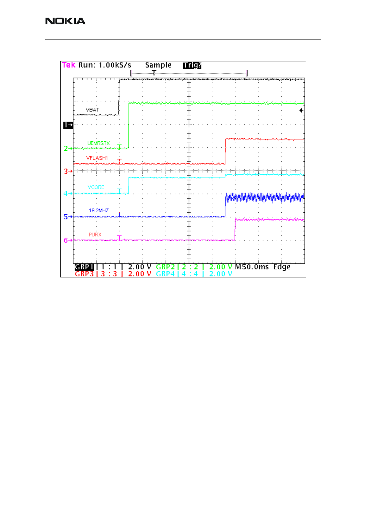
3125 (RH-61)
Nokia Customer Care BB Description and Troubleshooting
Power Up - Power Key
When the Power key is pressed, the UEM enters the power-up sequence. Pressing the
Power key causes the PWRONX pin on the UEM to be grounded. The UEM PWRONX
signal is not part of the keypad matrix. The Power key is only connected to the UEM. This
means that when pressing the power key an interrupt is generated to the UPP that starts
the MCU. The MCU then reads the UEM interrupt register and notices that it is a
PWRONX interrupt. The MCU reads the status of the PWRONX signal using the UEM
control bus (CBUS). If the PWRONX signal stays low for a certain time the MCU accepts
this as a valid power-on state and continues with the SW initialization of the baseband.
If the Power key does not indicate a valid power-on situation, the MCU powers off the
baseband.
Power Up - Charger
In order to be able to detect and start charging in cases where the main battery is fully
discharged (empty) and the UEM has no supply (NO_SUPPLY or BACKUP mode of UEM),
charging is controlled by start-up charging circuitry.
Whenever the VBAT level is detected to be below the master reset threshold (V
charging is controlled by start-up charging circuitry. Connecting a charger forces the
Figure 3: Measured power-on sequence and timing
MSTR-
),
Issue 1 08/2004 ©2004 Nokia Corporation Company Confidential Page 7
Page 81

3125 (RH-61)
BB Description and Troubleshooting
VCHAR input to rise above the charger detection threshold (VCH
start-up charging is initiated. The UEM generates 100 mA constant output current from
the connected charger’s output voltage. The battery’s voltage rises at it charges, and
when the VBAT voltage level is detected to be higher than the master reset threshold
limit (V
), the start-up charge is terminated.
MSTR+
Monitoring the VBAT voltage level is done by a charge control block (CHACON). A
MSTRX=‘1’ output reset signal (internal to the UEM) is given to the UEM’s RESET block
when the VBAT>V
If the VBAT is detected to fall below V
cancelled. It will restart if a new rising edge on the VCHAR input is detected (VCHAR
rising above VCH
Power Up - RTC Alarm
If the phone is in power-off mode when an RTC alarm occurs, the wake-up procedure
occurs. After the baseband is powered on, an interrupt is given to the MCU. When an RTC
alarm occurs during active mode, the interrupt is generated to the MCU.
Power Off
MSTR+
DET+
and the UEM enters into the reset sequence.
during start-up charging, charging is
MSTR
).
) and by detection,
DET+
The baseband switches to power-off mode if any of following occurs:
• Power key is pressed
• Battery voltage is too low (VBATT < 3.2 V)
• Watchdog timer register expires
The UEM controls the power-down procedure.
Power Consumption and Operation Modes
In POWER-OFF mode, the power (VBAT) is supplied to the UEM, buzzer, vibra, LED, PA,
and PA drivers. During this mode, the current consumption is approximately 35 uA.
In Sleep Mode, both processors (MCU and DSP) are in stand-by mode. The phone enters
sleep mode only when both processors make this request. When the SLEEPX signal is
detected low by the UEM, the phone enters SLEEP mode. The VIO and VFLASH1
regulators are put into low quiescent current mode, VCORE enters LDO mode, and the
VANA and VFLASH2 regulators are disabled. All RF regulators are disabled during SLEEP
mode. When the SLEEPX signal is detected high by the UEM, the phone enters ACTIVE
mode and all functions are activated.
Sleep mode is exited either by the expiration of a sleep clock counter in the UEM or by
some external interrupt (generated by a charger connection, key press, headset
connection, etc.).
In sleep mode, the VCTCXO is shut down and the 32 kHz sleep clock oscillator is used as
a reference clock for the baseband.
Page 8 ©2004 Nokia Corporation Company Confidential Issue 1 08/2004
Page 82

3125 (RH-61)
Nokia Customer Care BB Description and Troubleshooting
The average current consumption of the phone in sleep mode can vary depending mainly
on the SW state (e.g., slot cycle 0, 1, or 2) and if the phone is working on IS95 or IS2000
for CDMA. However, the average consumption is about 6 mA in slot cycle 0 on IS95.
In the Active Mode, the phone is in normal operation, scanning for channels, listening to
a base station, transmitting and processing information. There are several sub-states in
the active mode depending on the present state of the phone, such as burst reception,
burst transmission, if the DSP is working, etc.
In active mode, SW controls the VR1A and VR1B UEM RF regulators, which can be
enabled or disabled. VSIM can be enabled or disabled and its output voltage can be
programmed to be 1.8 V or 3.3 V. VR2 and VR4—VR7 can be enabled, disabled, or forced
into low quiescent current mode. VR3 is always enabled in active mode and disabled
during sleep mode and cannot be controlled by SW in the same way as the other
regulators. VR3 will only turn off if both processors request to be in sleep mode.
Charging Mode can be performed in parallel with any other operating mode. A BSI
resistor inside the battery pack indicates the battery type/size. The resistor value
corresponds to a specific battery capacity. This capacity value is related to the battery
technology.
The battery voltage, temperature, size, and charging current are measured by the UEM
and the charging software running in the UPP controls it.
The charging control circuitry (CHACON) inside the UEM controls the charging current
delivered from the charger to the battery and phone. The battery voltage rise is limited
by turning the UEM switch off when the battery voltage has reached 4.2 V. The charging
current is monitored by measuring the voltage drop across a 220 mOhm resistor.
Power Distribution
In normal operation, the baseband is powered from the phone‘s battery. The battery
consists of one Lithium-Ion cell capacity of 850 mAh and some safety and protection
circuits to prevent harm to the battery.
The UEM ASIC controls the power distribution to the whole phone through the BB and RF
regulators excluding the power amplifier (PA), which has a continuous power rail directly
from the battery. The battery feeds power directly to the following parts of the system:
•UEM
•PA
• Buzzer
•Vibra
•Display
• Keyboard lights
The heart of the power distribution to the phone is the power control block inside the
Issue 1 08/2004 ©2004 Nokia Corporation Company Confidential Page 9
Page 83

3125 (RH-61)
BB Description and Troubleshooting
UEM. It includes all the voltage regulators and feeds the power to the whole system. The
UEM handles hardware power-up functions so the regulators are not powered and the
power up reset (PURX) is not released if the battery voltage is less than 3 V.
The baseband is powered from five different UEM regulators.
Table 1: Baseband Regulators
Regulator
VCORE 300
VIO 150 1.8 Enabled always except during power-off mode
VFLASH1 70 2.78 Enabled always except during power-off mode
VFLASH2 40 2.78 Enabled only when data cable is connected
VANA 80 2.78 Enabled only when the system is awake (Off
VSIM 25 3.0 Enabled only when SIM card is used
Maximum
Current (mA)
400
Vout (V) Notes
1.5
1.35
Output voltage selectable 1.0V/1.3V.
Power up default value is 1.35V.
during sleep and power off-modes)
Table 2 includes the UEM regulators for the RF.
Table 2: RF Regulators
Regulator
VR1A 10 4.75 Enabled when cell transmitter is on
Maximum
Current (mA)
Vout (V) Notes
VR1B 10 4.75 Enabled when the transmitter is on
VR2 100 2.78 Enabled when the transmitter is on
VR3 20 2.78 Enabled when SleepX is high
VR4 50 2.78 Enabled when the receiver is on
VR5 50 2.78 Enabled when the receiver is on
VR6 50 2.78 Enabled when the transmitter is on
VR7 45 2.78 Enabled when the receiver is on
The charge pump that is used by VR1A is constructed around the UEM. The charge pump
works with the Cbus (1.2 MHz) oscillator and gives a 4.75 V regulated output voltage to
the RF.
Page 10 ©2004 Nokia Corporation Company Confidential Issue 1 08/2004
Page 84

3125 (RH-61)
Nokia Customer Care BB Description and Troubleshooting
Clock Distribution
RFClk (19.2 MHz Analog)
The main clock signal for the baseband is generated from the voltage and temperature
controlled crystal oscillator VCTCXO (G500). This 19.2 MHz clock signal is generated at
the RF and is fed to Yoda pin 18 (TCXO_IN) at C711. Yoda then converts the analog sine
waveform to a digital waveform with a swing voltage of 0 tot 1.8 V and sends it to the
UPP from pin 16 at Yoda (19.2 Out) to the UPP pin M5 (RFCLK).
Figure 4: Waveform of the 19.2 MHz clock (VCTCXO) going to the Yoda ASIC
Issue 1 08/2004 ©2004 Nokia Corporation Company Confidential Page 11
Page 85

3125 (RH-61)
BB Description and Troubleshooting
Figure 5 shows the RFCLK signal for the UPP.
Figure 5: Waveform of the 19.2 MHz Clk going to the UPP for Yoda ASIC
Page 12 ©2004 Nokia Corporation Company Confidential Issue 1 08/2004
Page 86

3125 (RH-61)
Nokia Customer Care BB Description and Troubleshooting
RFConvClk (19.2 MHz digital)
The UPP distributes the 19.2 MHz internal clock to the DSP and MCU, where the SW
multiplies this clock by seven for the DSP and by two for the MCU.
Figure 6: RFCovCLk waveform
Issue 1 08/2004 ©2004 Nokia Corporation Company Confidential Page 13
Page 87
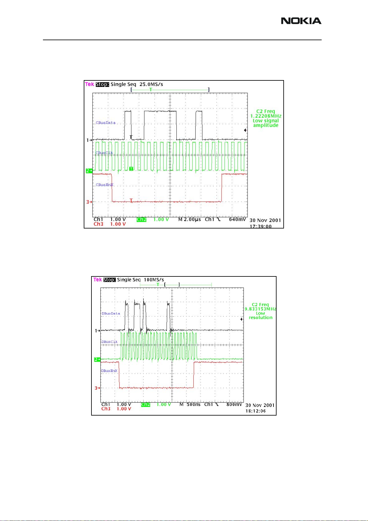
3125 (RH-61)
BB Description and Troubleshooting
CBUSClk Interface
A 1.2 MHz clock signal is used for CBUS, which is used by the MCU to transfer data
between the UEM and UPP.
DBUS Clk Interface
A 9.6 MHz clock signal is used for DBUS, which is used by the DSP to transfer data
between the UEM and UPP.
Figure 7: Cbus Data Transfer
Figure 8: Dbus data transferring
The system clock is stopped during sleep mode by disabling the VCTCXO power supply
(VR3) from the UEM regulator output by turning off the controlled output signal SleepX
from the UPP.
Page 14 ©2004 Nokia Corporation Company Confidential Issue 1 08/2004
Page 88
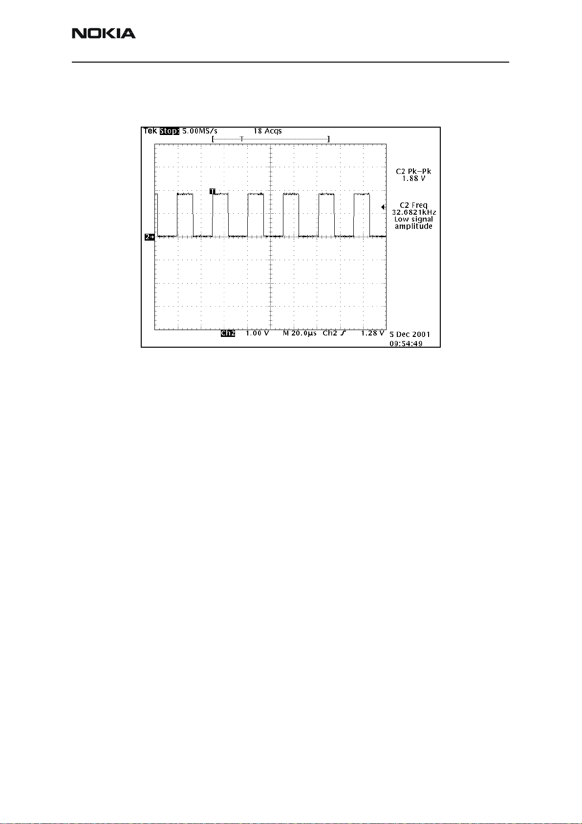
3125 (RH-61)
Nokia Customer Care BB Description and Troubleshooting
SleepCLK (Digital)
The UEM provides a 32 kHz sleep clock for internal use and to the UPP, where it is used
for sleep mode timing.
Figure 9: 32 kHz Digital output from UEM
Issue 1 08/2004 ©2004 Nokia Corporation Company Confidential Page 15
Page 89

3125 (RH-61)
BB Description and Troubleshooting
SleepCLK (Analog)
When the system enters sleep mode or power off mode, the external 32 KHz crystal
provides a reference to the UEM RTC circuit to turn on the phone during power off or
sleep mode.
Figure 10: 32 kHz analog waveform at 32 KHz crystal input
Flash Programming
Connections to Baseband
The flash programming equipment is connected to the baseband using test pads for
galvanic connection. The test pads are allocated in such a way that they can be accessed
when the phone is assembled. The flash programming interface uses the VPP, FBUSTX,
FBUSRX, MBUS, and BSI connections for the connection to the baseband. The connection
is through the UEM, which means that the logic levels corresponding to 2.7 V. Power is
supplied using the battery contacts.
Baseband Power Up
The baseband power is controlled by the flash prommer in production and in
reprogramming situations. The baseband powers up by applying supply voltage to the
battery terminals. Once the baseband is powered, flash programming indication begins
(see the following "Flash Programming Indication" section).
Flash Programming Indication
Flash programming is indicated to the UPP using the MBUSRX signal between the UPP
and UEM. The MBUS signal from the baseband to the flash prommer is used as a clock
for the synchronous communication. The flash prommer keeps the MBUS line low during
UPP boot to indicate that the flash prommer is connected. If the UPP MBUSRX signal is
low on UPP, the MCU enters flash programming mode. In order to avoid accidental entry
to the flash-programming mode, the MCU waits for a specified time to get input data
from the flash prommer. If the timer expires without any data being received, the MCU
Page 16 ©2004 Nokia Corporation Company Confidential Issue 1 08/2004
Page 90

3125 (RH-61)
Nokia Customer Care BB Description and Troubleshooting
continues the boot sequence. The MBUS signal from the UEM to the external connection
is used as a clock during flash programming. This means that the flash-programming
clock is supplied to the UPP on the MBUSRX signal.
The flash prommer indicates flash programming/reprogramming to the UEM by writing
an 8-bit password to the UEM. The data is transmitted on the FBUSRX line and the UEM
clocks the data on the FBUSRX line into a shift register. When the 8 bits have been
shifted in the register, the flash prommer generates a falling edge on the BSI line. This
loads the shift register content in the UEM into a compare register. If the 8 bits in the
compare register matches with the default value preset in the UEM, the flash prommer
pulls the MBUS signal to UEM low in order to indicate to the MCU that the flash
prommer is connected. The UEM reset state machine performs a reset to the system,
PURX low, for 20 ms. The UEM flash programming mode is valid until the MCU sets a bit
in the UEM register that indicates the end of flash programming. Setting this bit also
clears the compare register in the UEM, which was loaded at the falling edge of the BSI
signal. The UEM watchdogs are disabled during the flash programming mode. Setting the
bit indicating the end of flash programming enables and resets the UEM watchdog timer
to its default value. Clearing the flash programming bit also causes the UEM to generate
a reset to the UPP.
Flashing
The BSI signal is used to load the value into the compare register. In order to avoid
spurious loading of the register, the BSI signal is gated during UEM master reset and
during power on when PURX is active. The BSI signal should not change states during
normal operation unless the battery is extracted. In this case, the BSI signal will be
pulled high. Note that a falling edge is required to load the compare register.
Flash programming is done through the VPP, FBUSTX, FBUSRX, MBUS, and BSI signals.
When the phone enters the flash programming mode, the prommer indicates to the UEM
that flash programming will take place by writing an 8-bit password to the UEM. The
prommer sets the BSI value to “1” and then uses FBUSRX for writing and MBUS for
clocking. The BSI is then set back to “0”.
The MCU uses the FBUSTX signal to indicates to the prommer that it has been noticed.
After this, it reports the UPP type ID and is ready to receive the secondary boot code to
its internal SRAM.
Issue 1 08/2004 ©2004 Nokia Corporation Company Confidential Page 17
Page 91
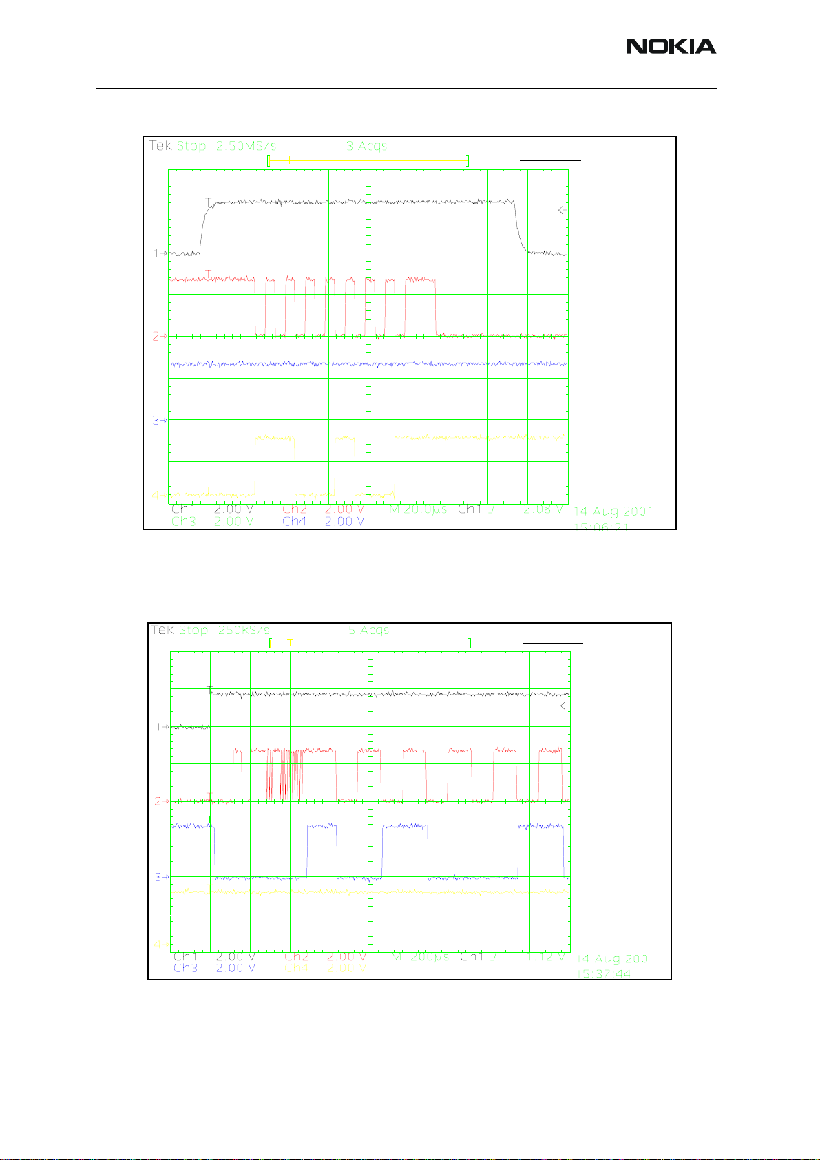
3125 (RH-61)
BB Description and Troubleshooting
FLASH_1
CH1 = BSI
CH2 = MBUS
CH3 = FBUSTX
CH4 = FBUSRX
Measure points
Production test pattern
(J396)
Figure 11: Flashing starts by BSI being pulled up and password being sent to UEM
This boot code asks the MCU to report the phone’s configuration information to the
prommer, including the flash device type. The prommer can then select and send
algorithm code to the MCU SRAM (and SRAM/Flash self-tests can be executed).
FLASH_2
CH1 = PURX
CH2 = MBUS
CH3 = FBUSTX
CH4 = FBUSRX
Measure points
Produc tion test pa ttern
(J396)
Figure 12: Flashing, continued
Page 18 ©2004 Nokia Corporation Company Confidential Issue 1 08/2004
Page 92
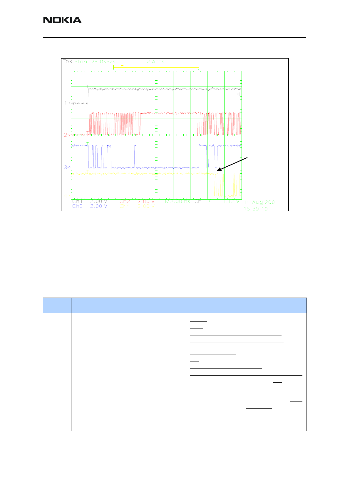
3125 (RH-61)
Nokia Customer Care BB Description and Troubleshooting
FLASH_3
CH1 = PURX
CH2 = MBUS
CH3 = FBUSTX
CH4 = FBUSRX
Measure points
Produc tion test pa ttern
(J396)
Data transfer has
started (Fbus_Rx)
Figure 13: Flashing, continued 2
Flash Programming Error Codes
The following characteristics apply to the information in Table 3.
• Error codes can be seen from the test results or from Phoenix's flash-tool.
• Underlined information means that the connection under consideration is being
used for the first time.
Table 3: Flash Programming Error Codes
Error Description Not Working Properly
C101 "The Phone does not set FbusTx line high after
the startup."
C102 "The Phone does not set FbusTx line low after
the line has been high. The Prommer generates
this error also when the Phone is not connected to the Prommer."
Vflash1
VBatt
BSI and FbusRX from prommer to UEM.
FbusTx from UPP->UEM->Prommer(SA0)
PURX(also to Safari)
VR3
Rfclock(VCTCXO->Safari->UPP)
Mbus from Prommer->UEM->UPP(MbusRx)(SA0)
FbusTx from UPP->UEM->Prommer(SA1)
BSI and FbusRX from prommer to UEM.
C103 " Boot serial line fail." Mbus from Prommer->UEM->UPP(MbusRx)(SA1)
FbusRx from Prommer->UEM->UPP
FbusTx from UPP->UEM->Prommer
C104 "MCU ID message sending failed in the Phone." FbusTx from UPP->UEM->Prommer
Issue 1 08/2004 ©2004 Nokia Corporation Company Confidential Page 19
Page 93
3125 (RH-61)
BB Description and Troubleshooting
Table 3: Flash Programming Error Codes (Continued)
Error Description Not Working Properly
C105 "The Phone has not received Secondary boot
codes length bytes correctly."
C106 "The Phone has not received Secondary code
bytes correctly."
C107 "The Phone MCU can not start Secondary code
correctly."
C586 "The erasing status response from the Phone
informs about fail."
C686 "The programming status response from the
Phone informs about fail."
Cx81 "The Prommer has detected a checksum error
in the message, which it has received from the
Phone."
Cx82 "The Prommer has detected a wrong ID byte in
the message, which it has received from the
Phone."
A204
Cx83
Cx84
"The flash manufacturer and device IDs in the
existing algorithm files do not match with the
IDs received from the target phone."
"The Prommer has not received phone
acknowledge to the message."
"The phone has generated NAK signal during
data block transfer."
Mbus from Prommer->UEM->UPP(MbusRx)
FbusRx from Prommer->UEM->UPP
FbusTx from UPP->UEM->Prommer
Mbus from Prommer->UEM->UPP(MbusRx)
FbusRx from Prommer->UEM->UPP
FbusTx from UPP->UEM->Prommer
UPP
Flash
Flash
FbusTx from UPP->UEM->Prommer
FbusTx from UPP->UEM->Prommer
Flash
UPP
VIO/VANA
Signals between UPP-Flash
Mbus from Prommer->UEM->UPP(MbusRx)
FbusRx from Prommer->UEM->UPP
FbusTx from UPP->UEM->Prommer
Cx85
Cx87 "Wrong MCU ID." RFClock
Startup
for
flashing
"Data block handling timeout"
UPP(Vcore)
Required startup for flashing Vflash1
VBatt
Page 20 ©2004 Nokia Corporation Company Confidential Issue 1 08/2004
Page 94

3125 (RH-61)
Nokia Customer Care BB Description and Troubleshooting
Charging Operation
Battery
The 3125 uses a Lithium-Ion cell battery with a capacity of 850 mAh. A resistor reading
inside the battery pack on the BSI line indicates the battery size. An NTC resistor close to
the SIM connector measures the phone’s temperature on the BTEMP line.
Temperature and capacity information are needed for charge control. These resistors are
connected to the BSI pins on the UEM. The phone has 100KΏ pull-up resistors for these
lines so that they can be read by A/D inputs in the phone.
Figure 14: BL-5C battery pack pin order
Charging Circuitry
The UEM ASIC controls charging depending on the charger being used and the battery
size. External components are needed for EMC, reverse polarity, and transient protection
of the input to the baseband module. The charger connection is through the system
connector interface. The 3125 baseband is designed to support DCT3 chargers from an
electrical point of view. Both 2- and 3-wire type chargers are supported. For the 3-wire
charger, the control line is not supported and not connected to the baseband ASICs.
R200
V100 battery
Figure 15: Charging circuitry
Issue 1 08/2004 ©2004 Nokia Corporation Company Confidential Page 21
Page 95

3125 (RH-61)
BB Description and Troubleshooting
Charger Detection
Connecting a charger creates voltage on the VCHAR input of the UEM. Charging starts
when the UEM detects the VCHAR input voltage level above 2 V (VCHdet+ threshold).
The VCHARDET signal is generated to indicate the presence of the charger for the SW.
The EM SW controls the charger identification/acceptance.
The charger recognition is initiated when the EM SW receives a ”charger connected”
interrupt. The algorithm basically consists of the following three steps:
1. Check that the charger output (voltage and current) is within safety limits
2. Identify the charger as a 2- or 3-wire charger
3. Check that the charger is within the charger window (voltage and current)
If the charger is accepted and identified, the appropriate charging algorithm is initiated.
X102
1
Charge Control
In active mode, charging is controlled by the UEM’s digital part. Charging voltage and
current monitoring is used to limit charging into safe area. For this reason, the UEM has
the following programmable charge cut-off limits:
• VBATLim1=3.6 V (Default)
• VBATLim2L=5.0 V
• VBATLim2H=5.25 V
VBATLim1, 2L, 2H are designed with hystereses. When the voltage rises above VBATLim1,
2L, 2H+ charging is stopped by turning the charging switch off. No change is done in
operational mode. After the voltage has decreased below VBATLim-, charging restarts.
F100
1.5A
L1002
________
42R/100MHz
Figure 16: Charging circuit
V100
"VCHARIN"
C106
1n0
0
2
CHARGER(4:0)
There are two PWM frequencies in use depending on the type of the charger. A 2-wire
charger uses a 1 Hz, while a 3-wire charger uses a 32Hz. The duty cycle range is 0% to
100%. The maximum charging current is limited to 1.2 A.
UEM Pins
N10
M10
R200
.22 Ohms
C201
1uF
C202
10nF
Figure 17: Charging circuity at the battery
Page 22 ©2004 Nokia Corporation Company Confidential Issue 1 08/2004
VBAT
Page 96
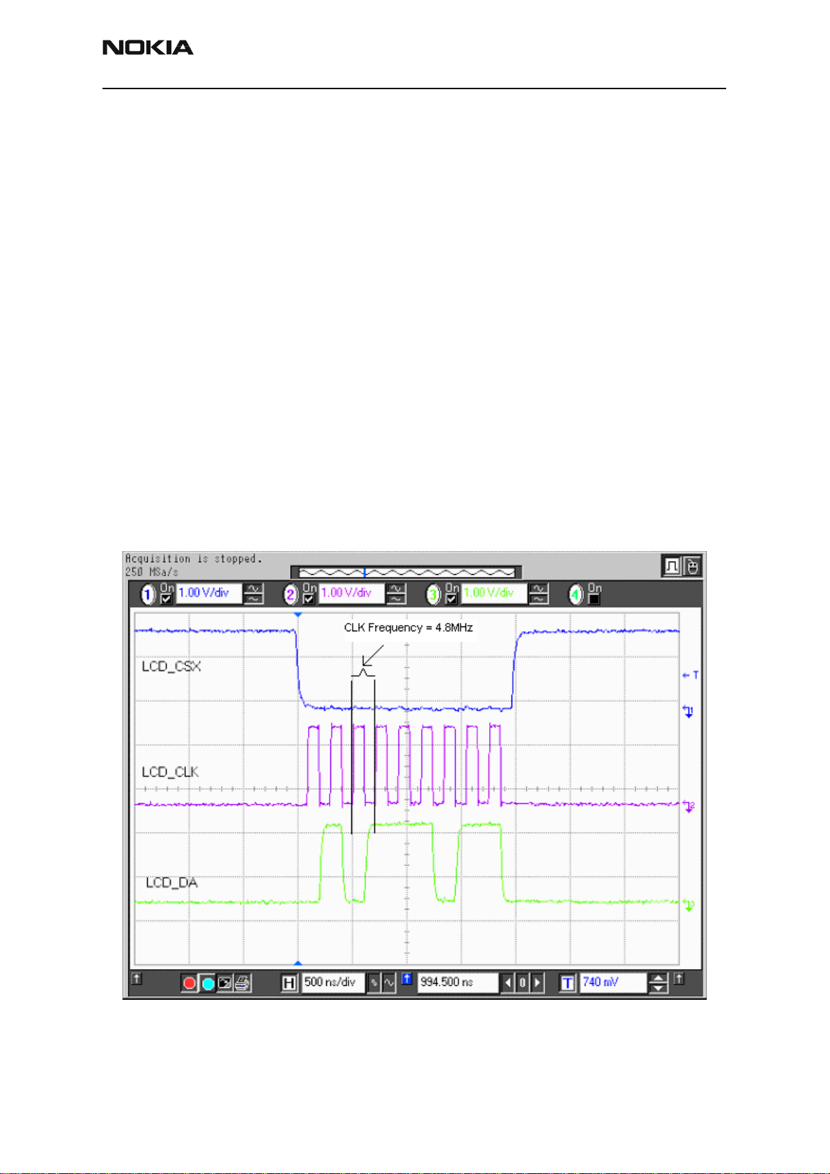
3125 (RH-61)
Nokia Customer Care BB Description and Troubleshooting
Audio
The audio control and processing in the 3125 is provided by the UEM, which contains the
audio codec, and the UPP, which contains the MCU and DSP blocks. These blocks handle
and process the audio data signals.
The baseband supports three microphone inputs and two earpiece outputs. The
microphone inputs are MIC1, MIC2, and MIC3. MIC1 input is used for the phone's
internal microphone; MIC2 input is used for headsets (HDB-4). MIC3 is not used. Every
microphone input can have either a differential or single-ended AC connection to UEM
circuit. In 3125 (RH-61), the internal microphone (MIC1) and external microphone
(MIC2) for Pop-PortTM accessory detection are both differential. The microphone signals
from different sources are connected to separate inputs at the UEM. Inputs for the
microphone signals are differential types. Also, MICBIAS1 is used for MIC1 and
MICBIAS2 is used for MIC2.
Display and Keyboard
The 3125 uses LEDs for the color LCD and keypad illumination. There are two LEDs for the
LCD and four LEDs for the keypad. KLIGHT is the signal used to drive the LED driver for
the LCD and keyboard. This signal turns on the LED driver. The interface uses a 9-bit data
transfer and is quite similar to the DCT3 type interface, except the Command/Data
information is transferred together with the data.
Figure 18: Waveform for the LCD Interface
Issue 1 08/2004 ©2004 Nokia Corporation Company Confidential Page 23
Page 97

3125 (RH-61)
BB Description and Troubleshooting
Accessories
The 3125 supports Pop-Port and Universal Headset accessories, differential and singleended, respectively. Detection of the Pop-Port accessories is done through the ACI signal
where the Universal Headset is detected on GenIO (12).
Figure 19: Pop-Port connector pin out
The pin out on the Pop-Port connector is as follows:
•Charger
• Charger GND
•ACI
•Vout
•USB Vbus
• USB D+ / Fbus Rx
• USB D- / Fbus Tx
• Data GND
•XMic N
•XMic P
•HSear N
•HSear P
•HSear R N
•HSear R P
You can perform the following in Pop-Port accessories:
• Charging
• Accessory detection
• FBUS communication
• USB communication
• Fully differential audio interface for mono- and stereo outputs
Page 24 ©2004 Nokia Corporation Company Confidential Issue 1 08/2004
Page 98

3125 (RH-61)
Nokia Customer Care BB Description and Troubleshooting
Charging
Charging through Pop-Port is accomplished in the same manner as through the charger
connector. Pin 1 of the Pop-Port is physically connected to the charger connector. When
the phone is connected to a desktop charger (e.g., DCV-15), it charges in the same
manner as it does with the charger connector.
Figure 20 shows the actual charging sequence. The channels on the diagram are:
• CH1 = Charging current across the .22 Ohm (R200) resistor on UEMK
• CH2 = Charger voltage measure at V100
• CH3 = Battery voltage measure at R200
•CH4 = PURX
Figure 20: Charging sequence
In Channel 4, PURX is released, which indicates when the phone operation goes from
RESET mode to POWER ON mode.
Issue 1 08/2004 ©2004 Nokia Corporation Company Confidential Page 25
Page 99
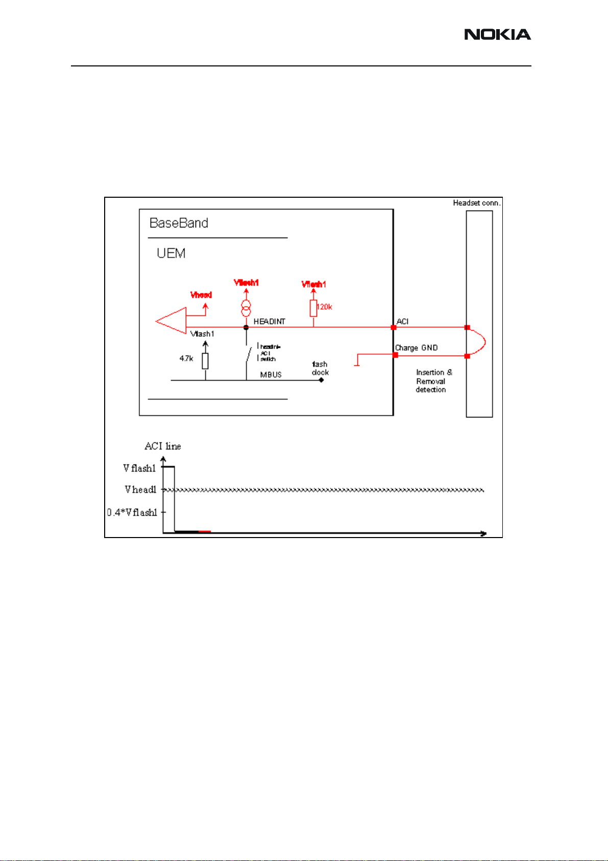
3125 (RH-61)
BB Description and Troubleshooting
Pop-Port Headset Detection
Accessory detection on the Pop-Port is done digitally. The pins used for this accessory
detection are:
• Pin 2 (Charge GND)
• Pin 3 (ACI)
•Pin 4 (Vout)
Figure 21: Waveform showing Pop-Port accessory detection
Page 26 ©2004 Nokia Corporation Company Confidential Issue 1 08/2004
Page 100

3125 (RH-61)
Nokia Customer Care BB Description and Troubleshooting
FBus Detection
FBus communication in Pop-Port is done through the following lines:
• Pin 2 (Charge GND)
• Pin 3 (ACI)
•Pin 4 (Vout)
• Pin 6 (FBus Rx)
• Pin 7 (FBus Tx)
Figure 22: Waveform showing Pop-Port FBus communication
Accessory Detection Through ACI
USB and Audio on (mono or stereo)/FM radio communication in Pop-Port is done through
the following signals:
Table 4: Accessory Detection Signals
USB Audio/FM
Pin 5 (USB Vbus) Pin 9 (XMic N)
Pin 6 (USB +) Pin 10 (SMIC P)
Pin 7 (USB -) Pin 11 (HSEAR N)
Pin 8 (Data GND) Pin 12 (HSEAR P)
Issue 1 08/2004 ©2004 Nokia Corporation Company Confidential Page 27
 Loading...