

Page 1

Customer Care Solutions
Technical Documentation
SERVICE
MANUAL
[NMP Part No. 0275932]
RH-6
Nokia 3108
Issue 1
COMPANY CONFIDENTIAL
Issue 1 10/2003
Copyright © 2003 Nokia. All Rights Reserved.
Page 2

Customer Care Solutions
Technical Documentation
Amendment Record Sheet
Amendment No Date Inserted By Comments
Issue 1 Oct 2003 Juho Korhonen Original Issue
Issue 1 10/2003 COMPANY CONFIDENTIAL 2
Copyright © 2003 Nokia. All Rights Reserved.
Page 3

Customer Care Solutions
Technical Documentation
Copyright © 2003 Nokia. All rights reserved.
Reproduction, transfer, distribution or storage of part or all of the contents in
this document in any form without the prior written permission of Nokia is prohibited.
Nokia, Nokia Connecting People, RH-6 and 3108 are trademarks or registered trademarks of Nokia Corporation. Other product and company names
mentioned herein may be trademarks or tradenames of their respective owners.
Nokia operates a policy of continuous development. Nokia reserves the righ t
to make changes and improvements to any of the products described in this
document without prior notice.
Under no circumstances shall Nokia be responsible for any loss of data or income or any special, incidental, consequential or indirect damages howsoever caused.
The contents of this document are provided "as is". Except as required by applicable law, no warranties of any kind, either express or implied, including,
but not limited to, the implied warranties of merchantability and fitness for a
particular purpose, are made in relation to the accuracy, reliability or contents
of this document. Nokia reserves the right to revise this document or withdraw it at any time without prior notice.
The availability of particular products may vary by region.
IMPORTANT
This document is intended for use by qualified service personnel
only.
Issue 1 10/2003 COMPANY CONFIDENTIAL 3
Copyright © 2003 Nokia. All Rights Reserved.
Page 4

Please refer to the RH-6 user guide for instructions relating to
operation, care and maintenance including important safety information. Note also the following:
Warnings:
1. IF THE DEVICE CAN BE INSTALLED IN A VEHICLE, CARE
MUST BE TAKEN ON INSTALLATION IN VEHICLES FITTED
WITH ELECTRONIC ENGINE MANAGEMENT SYSTEMS AND
ANTI-SKID BRAKING SYSTEMS. UNDER CERTAIN FAULT
CONDITIONS, EMITTED RF ENERGY CAN AFFECT THEIR
OPERATION. IF NECESSARY, CONSULT THE VEHICLE
DEALER/MANUFACTURER TO DETERMINE THE IMMUNITY
OF VEHICLE ELECTRONIC SYSTEMS TO RF ENERGY.
Customer Care Solutions
Technical Documentation
Warnings and Cautions
2. RH-6 MUST NOT BE OPERATED IN AREAS LIKELY TO CONTAIN POTENTIALLY EXPLOSIVE ATMOSPHERES EG PETROL STATIONS (SERVICE STATIONS), BLASTING AREAS
ETC.
3. OPERATION OF ANY RADIO TRANSMITTING EQUIPMENT,
INCLUDING CELLULAR TELEPHONES, MAY INTERFERE
WITH THE FUNCTIONALITY OF INADEQUATELY PROTECTED MEDICAL DEVICES. CONSULT A PHYSICIAN OR
THE MANUFACTURER OF THE MEDICAL DEVICE IF YOU
HAVE ANY QUESTIONS. OTHER ELECTRONIC EQUIPMENT
MAY ALSO BE SUBJECT TO INTERFERENCE.
Cautions:
1. Servicing and alignment must be undertaken by qualified personnel only.
2. Ensure all work is carried out at an anti-static workstation and
that an anti-static wrist strap is worn.
3. Ensure solder, wire, or foreign matter does not enter the telephone as damage may result.
4. Use only approved components as specified in the parts list.
5. Ensure all components, modules screws and insulators are correctly re-fitted after servicing and alignment. Ensure all cables
and wires are repositioned correctly.
Issue 1 10/2003 COMPANY CONFIDENTIAL 4
Copyright © 2003 Nokia. All Rights Reserved.
Page 5

Customer Care Solutions
Technical Documentation
For your safety
QUALIFIED SERVICE
Only qualified personnel may install or repair phone equipment.
ACCESSORIES AND BATTERIES
Use only approved accessories and batteries. Do not connect incompatible
products.
CONNECTING TO OTHER DEVICES
When connecting to any other device, read its user’s guide for detailed safety
instructions. Do not connect incompatible products.
ESD protection
Nokia requires that RH-6 service points have sufficient
ESD protection (against static electricity) when servicing
the device.
Any product of which the covers are removed must be handled with ESD protection. The SIM card can be replaced
without ESD protection if the product is otherwise ready for
use.
To replace the covers ESD protection must be applied.
All electronic parts of the product are susceptible to ESD.
Resistors, too, can be damaged by static electricity discharge.
All ESD sensitive parts must be packed in metallized protective bags during shipping and handling outside any ESD
Protected Area (EPA).
Every repair action involving opening the product or handling the product components must be done under ESD
protection.
ESD protected spare part packages MUST NOT be
opened/closed out of an ESD Protected Area.
For more information and local requirements about ESD
protection and ESD Protected Area, contact your local
Nokia After Market Services representative.
Issue 1 10/2003 COMPANY CONFIDENTIAL 5
Copyright © 2003 Nokia. All Rights Reserved.
Page 6

Customer Care Solutions
Technical Documentation
Battery information
Note that a new battery's full performance is achieved only after two or three
complete charge and discharge cycles!
The battery can be charged and discharged hundreds of times but it will
eventually wear out. When the operating time (talk-time and standby time) is
noticeably shorter than normal, it is time to buy a new battery.
Use only batteries approved by the phone manufacturer and recharge the
battery only with the chargers approved by the manufacturer. Unplug the
charger when not in use. Do not leave the battery connected to a charger for
longer than a week, since overcharging may shorten its lifetime. If left unused
a fully charged battery will discharge itself over time.
Temperature extremes can affect the ability of your battery to charge.
For good operation times with Ni-Cd/NiMh batteries, discharge the battery
from time to time by leaving the product switched on until it turns itself off (or
by using the battery discharge facility of any approved accessory available
for the product). Do not attempt to discharge the battery by any other means.
Use the battery only for its intended purpose.
Never use any charger or battery which is damaged.
Do not short-circuit the battery. Accidental short-circuiting can occur when a
metallic object (coin, clip or pen) causes direct connection of the + and - terminals of the battery (metal strips on the battery) for example when you carry
a spare battery in your pocket or purse. Short- circuiting the terminals may
damage the battery or the connecting object.
Leaving the battery in hot or cold places, such as in a closed car in summer
or winter conditions, will reduce the capacity and lifetime of the battery. Always try to keep the battery between 15°C and 25°C (59°F and 77°F). A
phone with a hot or cold battery may temporarily not work, even when the battery is fully charged. Batteries' performance is particularly limited in temperatures well below freezing.
Do not dispose of batteries in a fire!
Dispose of batteries according to local regulations (e.g. recycling). Do not dis-
pose as household waste.
Issue 1 10/2003 COMPANY CONFIDENTIAL 6
Copyright © 2003 Nokia. All Rights Reserved.
Page 7

Care and maintenance
RH-6 is a product of superior design and craftsmanship and should be trea ted with care. The suggestions below will help you to fulfil any warranty obligations and to enjoy this product for many years.
Keep the phone and all its parts and accessories out of the reach of small
children.
Keep the phone dry. Precipitation, humidity and all types of liquids or moisture can contain minerals that will corrode electronic circuits.
Do not use or store the phone in dusty, dirty areas. Its moving parts can be
damaged.
Do not store the phone in hot areas. High temperatures can shorten the life
of electronic devices, damage batteries, and warp or melt certain plastics.
Do not store the phone in cold areas. When it warms up (to its normal temperature), moisture can form inside, which may damage electronic circuit
boards.
Do not drop, knock or shake the phone. Rough handling can break internal
circuit boards.
Do not use harsh chemicals, cleaning solvents, or strong detergents to clean
the phone.
Do not paint the phone. Paint can clog the moving parts an d prevent proper
operation.
Use only the supplied or an approved replacement antenna. Unauthorised
antennas, modifications or attachments could damage the phone and may violate regulations governing radio devices.
All of the above suggestions apply equally to the product, battery, charger or
any accessory.
Page 8

Company Policy
Our policy is of continuous development; details of all technical modifications
will be included with service bulletins.
While every endeavour has been made to ensure the accuracy of this document, some errors may exist. If any errors are found by the reader, NOKIA
MOBILE PHONES Business Group should be notified in writing.
Please state:
Title of the Document + Issue Number/Date of publication
Latest Amendment Number (if applicable)
Page(s) and/or Figure(s) in error
Please send to:
NOKIA CORPORATION
Nokia Mobile Phones Business Group
CCS Technical Documentation
PO Box 86
FIN-24101 SALO
Finland
Page 9

Table of Contents
1 - General Information 2 - Parts Lists & Layouts 3 - Service Software & Service Concepts 4 - Service Tools 5 - Disassembly Instructions 6 - Baseband Description & Troubleshooting 7 - RF Description & Troubleshooting 8 - Schematics
Page 10

Customer Care Solutions
RH-6 Series Cellular Phones
1 - General Information
Issue 1 10/2003 Copyright © 2003 Nokia Corporation. Page 1
Company Confidential
Page 11

RH-6 Company Confidential
1 - General Information CCS Technical Documentation
Table of Contents
Page No
The Product.................................................................................................................... 3
Hand portable transceiver ............................................................................................3
The features of the RH-6, Nokia 3108 .........................................................................3
Sales package ...............................................................................................................6
General specifications of transceiver ...........................................................................6
Mobile enhancements ..................................................................................................7
Issue 1 10/2003 Copyright © 2003 Nokia Corporation. Page 2
Company Confidential
Page 12
Company Confidential RH-6
CCS Technical Documentation 1 - General Information
The Product
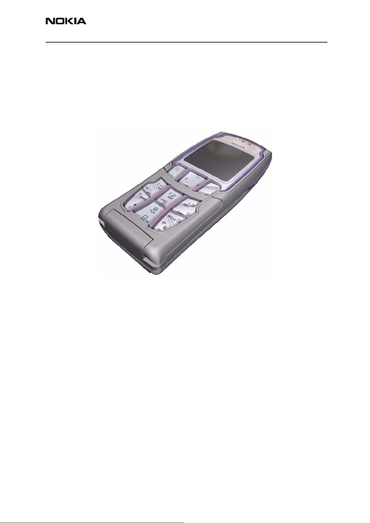
The RH-6, Nokia 3108, is a triple-band hand portable mobile telephone for the E-GSM
900, GSM 1800 and GSM 1900 networks, automatically switching between 900, 1800
and 1900MHz bands; automatic handover between 900 & 1800 MHz bands. It is power
class 1 (1W) transceiver in all bands except GSM900 where it is a power class 4 transceiver (2W).
Hand portable transceiver
The features of RH-6, Nokia 3108
Tri-band: E-GSM 900/GSM 1800/GSM 1900 16 polyphonic midi ring tones
WAP and GPRS (General Packet Radio Service) Internal vibra
HSCSD (High Speed Circuit Switched Data) Plug & play HF support
Full graphic colour display Internal antenna
Jack style UI with two soft keys Touchpad
Pen input with Chinese handwriting recognition
Automatic Key guard
Integrated handsfree speaker
Special features to meet the Chinese requirements
Pen input with Chinese handwriting recognition
• The most natural way of writing Chinese
• Predictive Chinese handwriting input
• More intuitive and faster way to write messages, taking notes or entering information
Issue 1 10/2003 Copyright © 2003 Nokia Corporation. Page 3
Company Confidential
Page 13

RH-6 Company Confidential
1 - General Information CCS Technical Documentation
• Enable text editor, number editor and search
• Also supports the English alphabet input and recognition
Lunar calendar for markets, except PRC mainland
• Records the important festival days and the lunar birthday
• Informs the user of the rhythm of the months
• Converts both the Gregorian to Lunar and Lunar to Gregorian calendars
Enhanced phonebook
• Easier phonebook searching
• Search by Pinyin and all character search
Chinese PC suite
• Enables handling the communication between PC and the phone
Other features of the RH-6, Nokia 3108
Ease of use
• Compact package which is both stylish and trendy
• Provided with a comfortable stylus
• Intuitive to use, Nokia series 40 user interface
• Ergonomically designed with a 4 way scroll key
• Large colour display
• High resolution 128 x 128 pixels
• 4096 colours
Full messaging support
• Entry of data using the pen input or ergonomic keymat
• Supports:
• Sending and receiving of multimedia messages using Multimedia Messaging Service (MMS)
• Enables text messages emphasized with still or animated pictures
• Can receive messages with sound, picture and text
• Can send and forward messages with image and text
• Short Message Service (SMS) sending and receiving with message concatenation
• Chatting on Mobile QQ (only for PRC mainland)
Personal Organizer
• Extensive calendar - Manages daily schedules, meetings and events
• View successive days with ease
• Busy view of a week
• Lunar calendar
• Improved notes view for one day
Issue 1 10/2003 Copyright © 2003 Nokia Corporation. Page 4
Company Confidential
Page 14

Company Confidential RH-6
CCS Technical Documentation 1 - General Information
• Snooze on calendar alarm
Personalization and Leisure
• Themed wallpapers
• Personalized applications with Java technology
• Pre-installed Java applications
• Pre-Installed Java games
Note: these pre-installed applications and games can be removed and replaced with MIDlets more
suitable to ones needs.
• Goto Menu
• Control of quick menus
• The setting of short cuts
Issue 1 10/2003 Copyright © 2003 Nokia Corporation. Page 5
Company Confidential
Page 15
RH-6 Company Confidential
1 - General Information CCS Technical Documentation
XHTML browser
• Full colour user interface
• Richer content
• Convergence of Web and Mobile content development
• New branding opportunities
Sales package
•Transceiver
• Charger ACP-12 and ACP-7 (country dependent)
• Battery BL-4C
• Standard Battery Cover
• Slim C-cover
• Standard Stylus
• Pocket Stylus
•User Guide
General specifications of transceiver
Parameter Unit
Cellular system GSM900, GSM1800, GSM1900
RX frequency band EGSM:
GSM900:
GSM1800:
GSM1900:
TX frequency band EGSM:
GSM900:
GSM1800:
GSM1900:
Output power EGSM:
GSM900:
GSM1800:
GSM1900:
Duplex spacing EGSM:
GSM900:
GSM1800:
GSM1900:
Number of RF channels EGSM:
GSM900:
GSM1800:
GSM1900:
Channel spacing 200 kHz (each band)
925 ... 935 MHz
935 ... 960 MHz
1805 ... 1880 MHz
1930 ... 1990 MHz
880 ... 890 MHz
890 ... 915 MHz
1710 ... 1785 MHz
1850 ... 1910 MHz
+5 ... +33 dBm (3.2 mW ... 2 W)
+5 ... +33 dBm (3.2 mW ... 2 W)
+0 ... +30 dBm (1.0 mW ... 1 W)
+0 ... +30 dBm (1.0 mW ... 1 W)
45 MHz
45 MHz
95 MHz
80 MHz
50
124
374
299
Issue 1 10/2003 Copyright © 2003 Nokia Corporation. Page 6
Company Confidential
Page 16
Company Confidential RH-6
CCS Technical Documentation 1 - General Information
Parameter Unit
Number of TX power levels EGSM:
GSM900:
GSM1800:
GSM1900:
Sensitivity, static channel EGSM:
GSM900:
GSM1800:
GSM1900:
15
15
16
16
-102 dBm
-102 dBm
-102 dBm (+25ºC)
-102 dBm
Frequency error, static channel < 0.1 ppm
RMS phase error < 5.0 º
Peak phase error < 20.0 º
Volume 83 cc with stylus
Weight 93 g
Length 106 mm (with the flip closed)
Width (max) 44.9 mm
Thickness (max) 24.2 mm (26 mm with stylus)
Talk time 2.5 - 4 hrs
Stand-by time 150 - 350 hrs.
Mobile enhancements
Audio Imaging
HS-5 Mono Headset HS-1C Camera Headset
HDB-4 Mono Headset PT-3 Fun Camera
LPS-4 Inductive Loopset
HS-2R Radio Headset
Car Power
BHF-1 Headrest Handsfree BL-4C Battery, 760 mAh, Li-ion
LCH-9 Mobile Charger ACP-7 Standard Charger
LCH-12 Mobile Charger ACP-12 Travel Charger
Data
DKU-5 Connectivity Adapter Cable
Issue 1 10/2003 Copyright © 2003 Nokia Corporation. Page 7
Company Confidential
Page 17

RH-6 Company Confidential
1 - General Information CCS Technical Documentation
[This page intentionally blank]
Issue 1 10/2003 Copyright © 2003 Nokia Corporation. Page 8
Company Confidential
Page 18

Customer Care Solutions
RH-6 Series Cellular Phones
2 - Parts Lists & Layouts
Issue 1 10/2003 © 2003 Nokia Corporation. Page 1
Company Confidential
Page 19

RH-6 Company Confidential
2 - Parts Lists & Layouts CCS Technical Documentation
Table of Contents
Page No
Exploded View of ‘A’, ‘B’, and Flip Cover Assemblies and Touch Pad Module .........3
Exploded View of Antenna Assembly and UI module...................................................6
Assembly parts list for antenna assembly and UI module ...........................................6
Parts list module -------- for RH-6 ...............................................................................8
Component layout diagram - Top ..............................................................................24
Component layout diagram - Bottom ........................................................................25
Page 2 © 2003 Nokia Corporation. Issue 1 10/2003
Page 20
Company Confidential RH-6
CCS T echnical Documentation 2 - Part s Lists & Layouts
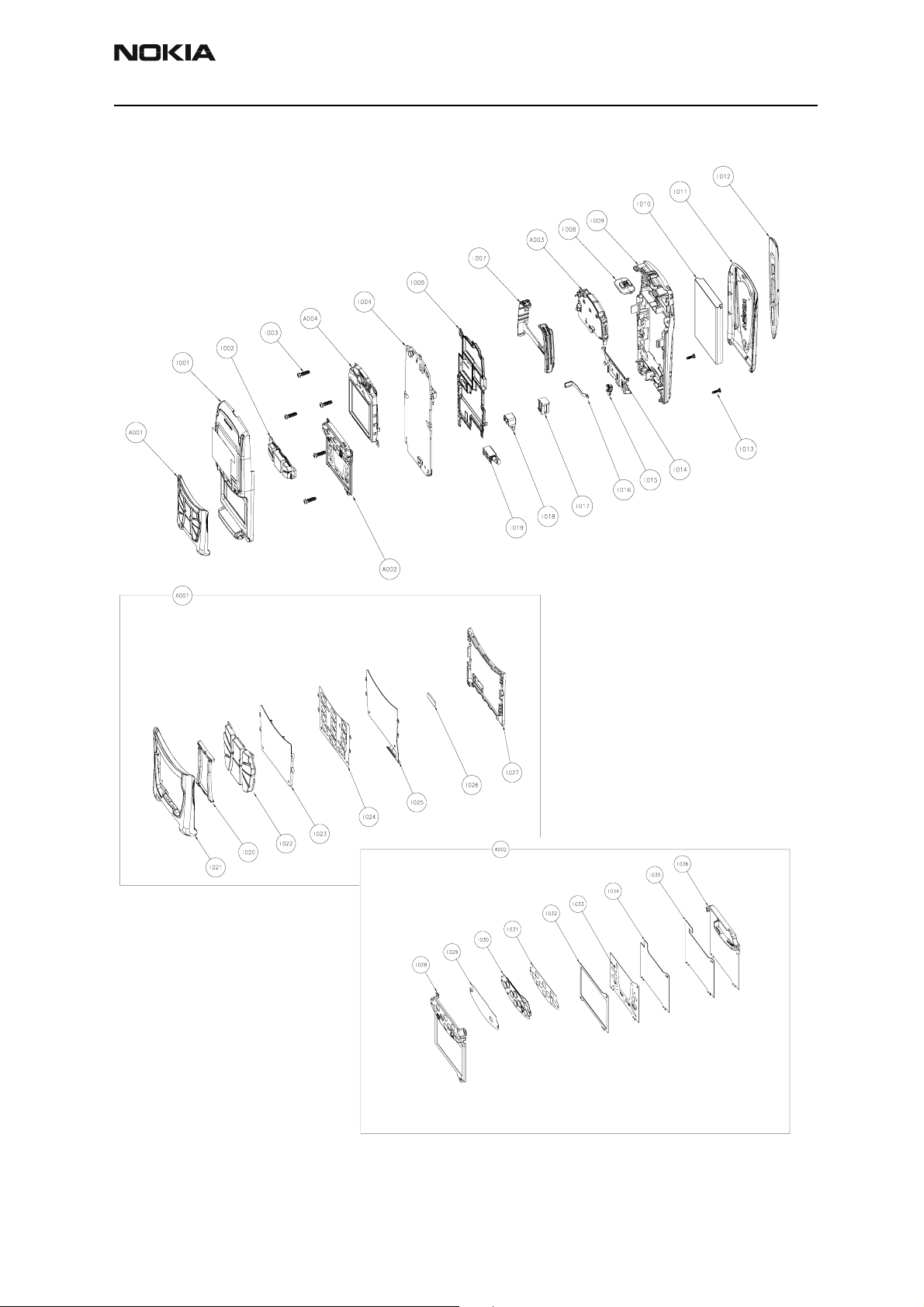
Exploded View of ‘A’, ‘B’, and Flip Cover Assemblies and Touch Pad Module
Issue 1 10/2003 © 2003 Nokia Corporation. Page 3
Page 21
RH-6 Company Confidential
2 - Parts Lists & Layouts CCS Technical Documentation
Assembly Parts List for ‘A’ Cover, ‘B’ Cover, Flip assy and Touch pad module
Item Description Available as a spare part
I001 A-cover assembly Yes
I002 Keymat function Yes
I003 Screw 1.8X6.0 T6 Yes
I004 PWB No
I005 Shielding assembly Yes
I006 Wrap right Yes
I007 Wrap left Yes
I008 Power key Yes
I009 B-cover assembly Yes
I010 Battery BL-4C No
I011 C-cover assembly Yes
I012 Stylus Yes
I013 Screw M1.6X5.3 Yes
I014 SIM Flap Yes
I015 Release button Yes
I016 Release spring Yes
I017 Connector DC-Jack 3.5mm Yes
I018 Mic. + Boot assembly Yes
I019 Vibra motor assembly Yes
A001 Flip assembly Yes
I020 Light rail No
I021 Flip cover assembly No
I022 Numerical keys No
I023 Keymat No
I024 Domesheet No
I025 Flip flex No
I026 Magnet No
I027 Flip back cover No
A002 Touch pad module Yes
I028 Touch pad shield No
I029 Touch pad panel No
Page 4 © 2003 Nokia Corporation. Issue 1 10/2003
Page 22
Company Confidential RH-6
CCS T echnical Documentation 2 - Part s Lists & Layouts
Item Description Available as a spare part
I030 Touch pad flex No
I031 Domesheet No
I032 Touch pad foam No
I033 Touch pad graphic sheet No
I034 Touch pad EL sheet No
I035 Touch pad carbon No
I036 Touch pad base No
For NMP codes, please refer to the Bill Of Repair (BOR) spare parts list.
Issue 1 10/2003 © 2003 Nokia Corporation. Page 5
Page 23
RH-6 Company Confidential
2 - Parts Lists & Layouts CCS Technical Documentation
Exploded View of Antenna Assembly and UI module
Assembly parts list for antenna assembly and UI module
Item Description Available as a spare part
A003 Antenna assembly Yes
I037 IHF Lid No
I038 IHF Pin No
Page 6 © 2003 Nokia Corporation. Issue 1 10/2003
Page 24
Company Confidential RH-6
CCS T echnical Documentation 2 - Part s Lists & Layouts
Item Description Available as a spare part
I039 Enclosure adhesive No
I040 Speaker No
I041 Speaker adhesive No
I042 IHF enclosure No
I043 Antenna radiator No
I044 B-cover gasket No
A004 UI module Yes
I045 UI shield assembly No
I046 Speaker Yes
I047 Locking clips No
I048 LCD module No
For NMP codes, please refer to the Bill Of Repair (BOR) spare parts list.
Issue 1 10/2003 © 2003 Nokia Corporation. Page 7
Page 25
RH-6 Company Confidential
2 - Parts Lists & Layouts CCS Technical Documentation
Parts list module -------- for RH-6
PWB components
Item
B200 4510219 Bottom M 5 CRYSTAL 32.768KHZ+-
B601 4510337 Bottom H 2 CRYSTAL 26.0MHZ+-
C100 2320546 Bottom F 7 Chipcap 5% NP0 27p 50V 0402C
C101 2320139 Top S 4 CHIPCAP X5R 1U0 K 10V
C102 2320481 Top S 4 CHIPCAP X5R 1U K 6V3
C103 2321013 Bottom R 7 CHIPCAP NP0 270P J
C104 2320544 Bottom R 7 Chipcap 5% NP0 22p 50V 0402C
C105 2320544 Bottom R 6 Chipcap 5% NP0 22p 50V 0402C
C106 2320744 Bottom S 3 Chipcap X7R 10% 50V
C107 2320778 Bottom T 7 Chipcap X7R 10% 16V
Product
code
Location
Side Grid Ref
Description and Value Type
32.768kHz ~ CRYSTAL_CX_4V
30PPM 9PF
26MHz ~ CRYSTAL_TSX_8
8PPM CL=15.5
1u0 10V 0603C_H0.95
0603
1u0 6.3V 0603C
0603
270p 25V 0402C
25V 0402
1n0 50V 0402C
0402
10n 16V 0402C
0402
A
C108 2320778 Bottom T 6 Chipcap X7R 10% 16V
0402
C109 2320778 Bottom T 7 Chipcap X7R 10% 16V
0402
C110 2320544 Bottom R 3 Chipcap 5% NP0 22p 50V 0402C
C111 2320778 Bottom T 7 Chipcap X7R 10% 16V
0402
C113 2320778 Top T 3 Chipcap X7R 10% 16V
0402
C150 2312243 Bottom O 7 CHIPCAP X5R 4U7 K 6V3
0805
C152 2312243 Bottom O 6 CHIPCAP X5R 4U7 K 6V3
0805
C153 2320783 Bottom N 6 CHIPCAP X7R 33N K 10V
0402
C155 2320805 Bottom N 5 CHIPCAP X5R 100N K
10V 0402
C156 2320544 Bottom T 7 Chipcap 5% NP0 22p 50V 0402C
10n 16V 0402C
10n 16V 0402C
10n 16V 0402C
10n 16V 0402C
4u7 6V3 0805C
4u7 6V3 0805C
33n 10V 0402C
100n 10V 0402C
Page 8 © 2003 Nokia Corporation. Issue 1 10/2003
Page 26
Company Confidential RH-6
CCS T echnical Documentation 2 - Part s Lists & Layouts
Item
C157 2320544 Bottom T 7 Chipcap 5% NP0 22p 50V 0402C
C158 2320805 Bottom N 6 CHIPCAP X5R 100N K
C159 2320783 Bottom N 6 CHIPCAP X7R 33N K 10V
C160 2320544 Bottom N 6 Chipcap 5% NP0 22p 50V 0402C
C161 2320744 Bottom N 6 Chipcap X7R 10% 50V
C162 2320805 Bottom N 6 CHIPCAP X5R 100N K
C163 2320481 Bottom O 6 CHIPCAP X5R 1U K 6V3
C164 2320544 Bottom N 5 Chipcap 5% NP0 22p 50V 0402C
C165 2320544 Bottom N 5 Chipcap 5% NP0 22p 50V 0402C
C166 2320783 Bottom N 7 CHIPCAP X7R 33N K 10V
Product
code
Location
Side Grid Ref
Description and Value Type
100n 10V 0402C
10V 0402
33n 10V 0402C
0402
1n0 50V 0402C
0402
100n 10V 0402C
10V 0402
1u0 6.3V 0603C
0603
33n 10V 0402C
0402
C167 2320139 Bottom N 5 CHIPCAP X5R 1U0 K 10V
0603
C168 2320805 Bottom O 6 CHIPCAP X5R 100N K
10V 0402
C169 2320544 Bottom N 6 Chipcap 5% NP0 22p 50V 0402C
C170 2320783 Bottom N 7 CHIPCAP X7R 33N K 10V
0402
C171 2320548 Bottom N 6 Chipcap 5% NP0 33p 50V 0402C
C172 2320548 Bottom N 7 Chipcap 5% NP0 33p 50V 0402C
C173 2320744 Bottom N 7 Chipcap X7R 10% 50V
0402
C174 2320744 Bottom N 7 Chipcap X7R 10% 50V
0402
C175 2316001 Bottom O 7 CHIPCAP X5R 2U2 K 6V3
0603
C176 2316001 Bottom O 7 CHIPCAP X5R 2U2 K 6V3
0603
C177 2320552 Bottom E 2 Chipcap 5% NP0 47p 50V 0402C
1u0 10V 0603C_H0.95
100n 10V 0402C
33n 10V 0402C
1n0 50V 0402C
1n0 50V 0402C
2u2 6V3 0603C
2u2 6V3 0603C
C178 2320552 Bottom E 2 Chipcap 5% NP0 47p 50V 0402C
C179 2320544 Bottom M 5 Chipcap 5% NP0 22p 50V 0402C
C180 2320544 Bottom M 5 Chipcap 5% NP0 22p 50V 0402C
Issue 1 10/2003 © 2003 Nokia Corporation. Page 9
Page 27
RH-6 Company Confidential
2 - Parts Lists & Layouts CCS Technical Documentation
Item
C181 2320544 Bottom O 7 Chipcap 5% NP0 22p 50V 0402C
C182 2320544 Bottom O 7 Chipcap 5% NP0 22p 50V 0402C
C183 2316001 Bottom O 7 CHIPCAP X5R 2U2 K 6V3
C184 2316001 Bottom O 7 CHIPCAP X5R 2U2 K 6V3
C185 2320744 Bottom N 6 Chipcap X7R 10% 50V
C200 2320805 Bottom L 6 CHIPCAP X5R 100N K
C201 2320481 Bottom K 5 CHIPCAP X5R 1U K 6V3
C202 2320778 Bottom K 5 Chipcap X7R 10% 16V
C203 2320481 Bottom N 8 CHIPCAP X5R 1U K 6V3
Product
code
Location
Side Grid Ref
Description and Value Type
2u2 6V3 0603C
0603
2u2 6V3 0603C
0603
1n0 50V 0402C
0402
100n 10V 0402C
10V 0402
1u0 6.3V 0603C
0603
10n 16V 0402C
0402
1u0 6.3V 0603C
0603
C204 2320481 Bottom K 5 CHIPCAP X5R 1U K 6V3
0603
C205 2320481 Bottom L 5 CHIPCAP X5R 1U K 6V3
0603
C206 2320481 Bottom L 5 CHIPCAP X5R 1U K 6V3
0603
C207 2320481 Bottom M 8 CHIPCAP X5R 1U K 6V3
0603
C208 2320481 Bottom K 5 CHIPCAP X5R 1U K 6V3
0603
C209 2320536 Bottom M 5 Chipcap 5% NP0 10p 50V 0402C
C210 2320536 Bottom N 5 Chipcap 5% NP0 10p 50V 0402C
C211 2320481 Bottom M 5 CHIPCAP X5R 1U K 6V3
0603
C212 2320481 Bottom P 5 CHIPCAP X5R 1U K 6V3
0603
C213 2320481 Bottom L 5 CHIPCAP X5R 1U K 6V3
0603
1u0 6.3V 0603C
1u0 6.3V 0603C
1u0 6.3V 0603C
1u0 6.3V 0603C
1u0 6.3V 0603C
1u0 6.3V 0603C
1u0 6.3V 0603C
1u0 6.3V 0603C
C214 2320481 Bottom L 5 CHIPCAP X5R 1U K 6V3
0603
C215 2320481 Bottom N 8 CHIPCAP X5R 1U K 6V3
0603
1u0 6.3V 0603C
1u0 6.3V 0603C
Page 10 © 2003 Nokia Corporation. Issue 1 10/2003
Page 28

Company Confidential RH-6
CCS T echnical Documentation 2 - Part s Lists & Layouts
Item
C218 2320805 Bottom K 8 CHIPCAP X5R 100N K
C219 2320481 Bottom K 5 CHIPCAP X5R 1U K 6V3
C220 2320778 Bottom N 5 Chipcap X7R 10% 16V
C221 2320481 Bottom K 6 CHIPCAP X5R 1U K 6V3
C222 2320481 Bottom J 6 CHIPCAP X5R 1U K 6V3
C223 2320481 Bottom K 6 CHIPCAP X5R 1U K 6V3
C224 2320481 Bottom K 7 CHIPCAP X5R 1U K 6V3
C225 2320481 Bottom K 7 CHIPCAP X5R 1U K 6V3
Product
code
Location
Side Grid Ref
Description and Value Type
10V 0402
0603
0402
0603
0603
0603
0603
0603
100n 10V 0402C
1u0 6.3V 0603C
10n 16V 0402C
1u0 6.3V 0603C
1u0 6.3V 0603C
1u0 6.3V 0603C
1u0 6.3V 0603C
1u0 6.3V 0603C
C226 2320481 Bottom J 7 CHIPCAP X5R 1U K 6V3
0603
C227 2320481 Bottom J 7 CHIPCAP X5R 1U K 6V3
0603
C228 2320481 Bottom J 8 CHIPCAP X5R 1U K 6V3
0603
C229 2320481 Bottom J 7 CHIPCAP X5R 1U K 6V3
0603
C230 2320481 Bottom K 7 CHIPCAP X5R 1U K 6V3
0603
C231 2320481 Bottom K 8 CHIPCAP X5R 1U K 6V3
0603
C232 2320481 Bottom K 7 CHIPCAP X5R 1U K 6V3
0603
C234 2320481 Bottom J 7 CHIPCAP X5R 1U K 6V3
0603
C235 2320481 Bottom L 5 CHIPCAP X5R 1U K 6V3
0603
C236 2320805 Bottom K 8 CHIPCAP X5R 100N K
10V 0402
1u0 6.3V 0603C
1u0 6.3V 0603C
1u0 6.3V 0603C
1u0 6.3V 0603C
1u0 6.3V 0603C
1u0 6.3V 0603C
1u0 6.3V 0603C
1u0 6.3V 0603C
1u0 6.3V 0603C
100n 10V 0402C
C237 2320805 Bottom K 8 CHIPCAP X5R 100N K
10V 0402
C238 2320805 Bottom L 5 CHIPCAP X5R 100N K
10V 0402
100n 10V 0402C
100n 10V 0402C
Issue 1 10/2003 © 2003 Nokia Corporation. Page 11
Page 29
RH-6 Company Confidential
2 - Parts Lists & Layouts CCS Technical Documentation
Item
C239 2320805 Bottom L 8 CHIPCAP X5R 100N K
C240 2320778 Bottom L 9 Chipcap X7R 10% 16V
C241 2320744 Bottom M 5 Chipcap X7R 10% 50V
C242 2320744 Bottom L 8 Chipcap X7R 10% 50V
C243 2320481 Bottom L 5 CHIPCAP X5R 1U K 6V3
C260 2320481 Bottom J 7 CHIPCAP X5R 1U K 6V3
C261 2320481 Bottom K 5 CHIPCAP X5R 1U K 6V3
C262 2320481 Bottom J 6 CHIPCAP X5R 1U K 6V3
Product
code
Location
Side Grid Ref
Description and Value Type
10V 0402
0402
0402
0402
0603
0603
0603
0603
100n 10V 0402C
10n 16V 0402C
1n0 50V 0402C
1n0 50V 0402C
1u0 6.3V 0603C
1u0 6.3V 0603C
1u0 6.3V 0603C
1u0 6.3V 0603C
C263 2320481 Bottom J 7 CHIPCAP X5R 1U K 6V3
0603
C264 2320481 Bottom J 7 CHIPCAP X5R 1U K 6V3
0603
C265 2320481 Bottom J 7 CHIPCAP X5R 1U K 6V3
0603
C300 2320805 Top B 6 CHIPCAP X5R 100N K
10V 0402
C301 2320805 Top C 6 CHIPCAP X5R 100N K
10V 0402
C302 2320556 Bottom O 8 Chipcap 5% NP0 68p 50V 0402C
C303 2320481 Bottom O 8 CHIPCAP X5R 1U K 6V3
0603
C304 2320125 Bottom M 8 CHIPCAP X5R 1U K 16V
0603
C305 2320125 Bottom M 8 CHIPCAP X5R 1U K 16V
0603
C306 2320778 Bottom Q 5 Chipcap X7R 10% 16V
0402
1u0 6.3V 0603C
1u0 6.3V 0603C
1u0 6.3V 0603C
100n 10V 0402C
100n 10V 0402C
1u0 6.3V 0603C
1u0 16V 0603C
1u0 16V 0603C
10n 16V 0402C
C309 2320481 Top S 3 CHIPCAP X5R 1U K 6V3
0603
C310 2320544 Bottom B 5 Chipcap 5% NP0 22p 50V 0402C
C312 2320544 Bottom F 2 Chipcap 5% NP0 22p 50V 0402C
1u0 6.3V 0603C
Page 12 © 2003 Nokia Corporation. Issue 1 10/2003
Page 30

Company Confidential RH-6
CCS T echnical Documentation 2 - Part s Lists & Layouts
Item
C313 2320544 Top B 4 Chipcap 5% NP0 22p 50V 0402C
C320 2320544 Top S 5 Chipcap 5% NP0 22p 50V 0402C
C321 2320544 Top T 5 Chipcap 5% NP0 22p 50V 0402C
C322 2320544 Top S 5 Chipcap 5% NP0 22p 50V 0402C
C323 2320544 Top U 5 Chipcap 5% NP0 22p 50V 0402C
C324 2320544 Top U 5 Chipcap 5% NP0 22p 50V 0402C
C330 2320584 Top L 6 Chipcap 5% X7R 1n0 50V 0402C
C331 2320584 Top L 6 Chipcap 5% X7R 1n0 50V 0402C
C332 2320584 Top L 6 Chipcap 5% X7R 1n0 50V 0402C
C333 2320584 Top L 6 Chipcap 5% X7R 1n0 50V 0402C
C343 2320805 Bottom P 5 CHIPCAP X5R 100N K
C344 2320805 Bottom N 5 CHIPCAP X5R 100N K
Product
code
Location
Side Grid Ref
Description and Value Type
100n 10V 0402C
10V 0402
100n 10V 0402C
10V 0402
C390 2320805 Bottom R 8 CHIPCAP X5R 100N K
10V 0402
C400 2320778 Bottom M 5 Chipcap X7R 10% 16V
0402
C401 2320805 Bottom M 5 CHIPCAP X5R 100N K
10V 0402
C402 2320778 Bottom L 5 Chipcap X7R 10% 16V
0402
C403 2320778 Bottom N 5 Chipcap X7R 10% 16V
0402
C404 2320778 Bottom N 5 Chipcap X7R 10% 16V
0402
C405 2320778 Bottom M 5 Chipcap X7R 10% 16V
0402
C420 2320552 Bottom L 5 Chipcap 5% NP0 47p 50V 0402C
C426 2320744 Bottom K 5 Chipcap X7R 10% 50V
0402
C450 2320778 Bottom Q 5 Chipcap X7R 10% 16V
0402
100n 10V 0402C
10n 16V 0402C
100n 10V 0402C
10n 16V 0402C
10n 16V 0402C
10n 16V 0402C
10n 16V 0402C
1n0 50V 0402C
10n 16V 0402C
C451 2320805 Bottom Q 5 CHIPCAP X5R 100N K
10V 0402
C454 2320779 Bottom Q 5 CHIPCAP X7R 100N K
16V 0603
100n 10V 0402C
100n 16V 0603_BLM
Issue 1 10/2003 © 2003 Nokia Corporation. Page 13
Page 31

RH-6 Company Confidential
2 - Parts Lists & Layouts CCS Technical Documentation
Item
C601 2320629 Bottom C 4 CHIPCAP NP0 1P0 B 50V
C602 2320629 Bottom C 3 CHIPCAP NP0 1P0 B 50V
C603 2320744 Bottom H 3 Chipcap X7R 10% 50V
C605 2320805 Bottom I 3 CHIPCAP X5R 100N K
C606 2320546 Bottom H 3 Chipcap 5% NP0 27p 50V 0402C
C607 2312211 Bottom G 2 CHIPCAP X5R 3U3 K 6V3
C610 2320805 Bottom L 4 CHIPCAP X5R 100N K
C615 2320778 Bottom G 3 Chipcap X7R 10% 16V
C620 2320546 Bottom G 3 Chipcap 5% NP0 27p 50V 0402C
Product
code
Location
Side Grid Ref
Description and Value Type
1p0 50V 0402C
0402
1p0 50V 0402C
0402
1n0 50V 0402C
0402
100n 10V 0402C
10V 0402
3u3 6V3 0805C_H1.35
0805
100n 10V 0402C
10V 0402
10n 16V 0402C
0402
C621 2320552 Bottom I 2 Chipcap 5% NP0 47p 50V 0402C
C622 2320805 Bottom I 3 CHIPCAP X5R 100N K
10V 0402
C623 2320805 Bottom I 4 CHIPCAP X5R 100N K
10V 0402
C624 2320546 Bottom H 5 Chipcap 5% NP0 27p 50V 0402C
C625 2320481 Bottom J 4 CHIPCAP X5R 1U K 6V3
0603
C626 2320522 Bottom G 5 Chipcap +-0.25pF NP0 2p7 50V 0402C
C627 2313213 Bottom J 2 CHIPCAP X5R 10U K 6V3
1206
C628 2320778 Bottom I 3 Chipcap X7R 10% 16V
0402
C629 2320546 Bottom I 4 Chipcap 5% NP0 27p 50V 0402C
C630 2320629 Bottom G 4 CHIPCAP NP0 1P0 B 50V
0402
C631 2320629 Bottom G 5 CHIPCAP NP0 1P0 B 50V
0402
100n 10V 0402C
100n 10V 0402C
1u0 6.3V 0603C
10u 6.3V 1206C_H1.8
10n 16V 0402C
1p0 50V 0402C
1p0 50V 0402C
C632 2320805 Bottom H 3 CHIPCAP X5R 100N K
10V 0402
C633 2320546 Bottom I 4 Chipcap 5% NP0 27p 50V 0402C
C634 2320522 Bottom G 3 Chipcap +-0.25pF NP0 2p7 50V 0402C
100n 10V 0402C
Page 14 © 2003 Nokia Corporation. Issue 1 10/2003
Page 32

Company Confidential RH-6
CCS T echnical Documentation 2 - Part s Lists & Layouts
Item
C635 2320546 Bottom I 4 Chipcap 5% NP0 27p 50V 0402C
C636 2320778 Bottom I 3 Chipcap X7R 10% 16V
C637 2320778 Bottom I 4 Chipcap X7R 10% 16V
C701 2320532 Bottom D 3 Chipcap +-0.25pF NP0 6p8 50V 0402C
C702 2320532 Bottom E 4 Chipcap +-0.25pF NP0 6p8 50V 0402C
C703 2320546 Bottom D 4 Chipcap 5% NP0 27p 50V 0402C
C705 2322023 Bottom I 5 CHIPCAP NP0 2N2 J 16V
C706 2320556 Bottom I 5 Chipcap 5% NP0 68p 50V 0402C
C709 2320631 Bottom I 5 CHIPCAP NP0 180P J
C710 2320631 Bottom I 4 CHIPCAP NP0 180P J
Product
code
Location
Side Grid Ref
Description and Value Type
10n 16V 0402C
0402
10n 16V 0402C
0402
2n2 16V 0603C
0603
180p 25V 0402C
25V 0402
180p 25V 0402C
25V 0402
C711 2310055 Bottom J 5 CHIPCAP NP0 3N9 J 25V
0805
C712 2320631 Bottom K 2 CHIPCAP NP0 180P J
25V 0402
C715 2320556 Bottom I 4 Chipcap 5% NP0 68p 50V 0402C
C716 2320556 Bottom I 3 Chipcap 5% NP0 68p 50V 0402C
C717 2320546 Bottom J 5 Chipcap 5% NP0 27p 50V 0402C
C718 2320744 Bottom I 5 Chipcap X7R 10% 50V
0402
C721 2320744 Bottom G 5 Chipcap X7R 10% 50V
0402
C722 2320540 Bottom F 5 Chipcap 5% NP0 15p 50V 0402C
C723 2320540 Bottom F 5 Chipcap 5% NP0 15p 50V 0402C
C731 2320550 Bottom G 5 Chipcap 5% NP0 39p 50V 0402C
C740 2312211 Bottom K 4 CHIPCAP X5R 3U3 K 6V3
0805
C741 2320635 Bottom K 2 CHIPCAP NP0 0P5 C 50V
0402
3n9 25V 0805C_AVX
180p 25V 0402C
1n0 50V 0402C
1n0 50V 0402C
3u3 6V3 0805C_H1.35
0p5 50V 0402C
C801 2320602 Bottom E 5 Chipcap +-0.25pF NP0 4p7 50V 0402C
C802 2320546 Bottom D 5 Chipcap 5% NP0 27p 50V 0402C
C803 2320546 Bottom C 4 Chipcap 5% NP0 27p 50V 0402C
Issue 1 10/2003 © 2003 Nokia Corporation. Page 15
Page 33

RH-6 Company Confidential
2 - Parts Lists & Layouts CCS Technical Documentation
Item
C804 2320546 Bottom C 4 Chipcap 5% NP0 27p 50V 0402C
C805 2320546 Bottom C 4 Chipcap 5% NP0 27p 50V 0402C
C807 2320520 Bottom C 5 Chipcap +-0.25pF NP0 2p2 50V 0402C
C811 2320744 Bottom C 5 Chipcap X7R 10% 50V
C812 2310793 Bottom I 8 CHIPCAP X5R 2U2 K 10V
C813 2320524 Bottom D 5 Chipcap +-0.25pF NP0 3p3 50V 0402C
C814 2320548 Bottom C 5 Chipcap 5% NP0 33p 50V 0402C
C815 2611753 Bottom I 7 CHIPTCAP 33U M 16V
C816 2320604 Bottom I 8 Chipcap 5% NP0 18p 50V 0402C
C817 2320602 Bottom I 8 Chipcap +-0.25pF NP0 4p7 50V 0402C
C818 2320546 Bottom D 8 Chipcap 5% NP0 27p 50V 0402C
Product
code
Location
Side Grid Ref
Description and Value Type
1n0 50V 0402C
0402
2u2 10V 0805C
0805
33u_16V 16V TANT_TPSW2
6.0X3.2X1.5
C819 2611753 Bottom B 7 CHIPTCAP 33U M 16V
6.0X3.2X1.5
C820 2320546 Bottom D 8 Chipcap 5% NP0 27p 50V 0402C
C821 2320518 Bottom D 8 Chipcap +-0.25pF NP0 1p8 50V 0402C
C822 2320546 Bottom D 8 Chipcap 5% NP0 27p 50V 0402C
C824 2320526 Bottom E 8 Chipcap +-0.25pF NP0 3p9 50V 0402C
C825 2320805 Bottom E 5 CHIPCAP X5R 100N K
10V 0402
C826 2320805 Bottom C 5 CHIPCAP X5R 100N K
10V 0402
C835 2320514 Bottom F 8 Chipcap +-0.25pF NP0 1p2 50V 0402C
C836 2320524 Bottom F 7 Chipcap +-0.25pF NP0 3p3 50V 0402C
C837 2320552 Bottom F 7 Chipcap 5% NP0 47p 50V 0402C
C872 2320805 Bottom H 2 CHIPCAP X5R 100N K
10V 0402
D200 4370959 Bottom L 7 UEMK_EDGE WDENA
TO25 TFBGA168
33u_16V 16V TANT_TPSW2
100n 10V 0402C
100n 10V 0402C
100n 10V 0402C
~ ~ uBGA168
D400 4375019 Bottom N 3 UPP8M V3.5 F751542I
UBGA144 C035
D450 4341531 Bottom P 3 COMBO 64M NOR + 4M
SRAM TBGA48
~ ~ uBGA144_CC
64M/4M ~ TBGA48
Page 16 © 2003 Nokia Corporation. Issue 1 10/2003
Page 34

Company Confidential RH-6
CCS T echnical Documentation 2 - Part s Lists & Layouts
Item
F100 5119019 Bottom S 3 SM FUSE F 1.5A 32V
G701 4350315 Bottom K 3 VCO 3420-3980MHZ
L100 3203705 Bottom S 3 FERRITE BEAD 42R/
L102 3203801 Bottom T 6 CHIP BEAD ARRAY
L103 3203801 Bottom T 7 CHIP BEAD ARRAY
L106 3203725 Bottom T 5 FERRITE BEAD 0R6
L107 3203741 Bottom T 6 FERRITE BEAD 0R5
L150 3203801 Top A 4 CHIP BEAD ARRAY
Product
code
Location
Side Grid Ref
Description and Value Type
0603
2.7V 19MA
100MHZ 0805
2X1000R 0405
2X1000R 0405
600R/100M 0402
600R/100MHZ 0603
2X1000R 0405
1.5A ~ 0603_FUSE
34203980MHz
42R/100MHz ~ 0805_FERRITE
2x1000R/
100MHz
2x1000R/
100MHz
600R/100MHz ~ FERRITE_0402
600R/100MHz ~ 0603_BLM
2x1000R/
100MHz
~ VCO_FDK_IT_H1.
7
~ 0405_2_MATSU
~ 0405_2_MATSU
~ 0405_2_MATSU
L151 3203769 Bottom E 2 FERR.BEAD 240R/100M
0.4A 0R4 0402
L152 3203769 Bottom E 2 FERR.BEAD 240R/100M
0.4A 0R4 0402
L153 3203725 Bottom S 4 FERRITE BEAD 0R6
600R/100M 0402
L260 3203741 Bottom I 7 FERRITE BEAD 0R5
600R/100MHZ 0603
L261 3203741 Bottom K 5 FERRITE BEAD 0R5
600R/100MHZ 0603
L262 3203741 Bottom I 6 FERRITE BEAD 0R5
600R/100MHZ 0603
L263 3203741 Bottom I 7 FERRITE BEAD 0R5
600R/100MHZ 0603
L264 3203741 Bottom I 7 FERRITE BEAD 0R5
600R/100MHZ 0603
L265 3203741 Bottom I 7 FERRITE BEAD 0R5
600R/100MHZ 0603
L300 3640119 Bottom N 7 CHOKE 22U M 1R4
0.33A 3.3X3.3X1.5
240R/100MHz ~ FERRITE_BK1005
240R/100MHz ~ FERRITE_BK1005
600R/100MHz ~ FERRITE_0402
600R/100MHz ~ 0603_BLM
600R/100MHz ~ 0603_BLM
600R/100MHz ~ 0603_BLM
600R/100MHz ~ 0603_BLM
600R/100MHz ~ 0603_BLM
600R/100MHz ~ 0603_BLM
22uH ~ CHOKE_984FB
L301 3646179 Top T 5 CHIP COIL 47N J Q23/
800MHZ 0402
L302 3646179 Top T 5 CHIP COIL 47N J Q23/
800MHZ 0402
47nH ~ 0402L
47nH ~ 0402L
Issue 1 10/2003 © 2003 Nokia Corporation. Page 17
Page 35

RH-6 Company Confidential
2 - Parts Lists & Layouts CCS Technical Documentation
Item
L303 3646179 Top T 5 CHIP COIL 47N J Q23/
L304 3646179 Top T 5 CHIP COIL 47N J Q23/
L305 3646179 Top S 5 CHIP COIL 47N J Q23/
L306 3646179 Top T 5 CHIP COIL 47N J Q23/
L307 3646179 Top S 5 CHIP COIL 47N J Q23/
L308 3646179 Top U 5 CHIP COIL 47N J Q23/
L309 3646179 Top U 5 CHIP COIL 47N J Q23/
L320 3203723 Top L 5 FERRITE BEAD 0R35
Product
code
Location
Side Grid Ref
Description and Value Type
800MHZ 0402
800MHZ 0402
800MHZ 0402
800MHZ 0402
800MHZ 0402
800MHZ 0402
800MHZ 0402
68R/100MHZ 0603
47nH ~ 0402L
47nH ~ 0402L
47nH ~ 0402L
47nH ~ 0402L
47nH ~ 0402L
47nH ~ 0402L
47nH ~ 0402L
68R/100MHz ~ FERRITE_BK1608
L321 3203723 Top K 6 FERRITE BEAD 0R35
68R/100MHZ 0603
L322 3203723 Top L 5 FERRITE BEAD 0R35
68R/100MHZ 0603
L323 3203723 Top L 6 FERRITE BEAD 0R35
68R/100MHZ 0603
L601 3646087 Bottom G 4 CHIP COIL 1N8+-0N3
Q31/800M 0402
L602 3646087 Bottom G 4 CHIP COIL 1N8+-0N3
Q31/800M 0402
L603 3646005 Bottom G 5 CHIP COIL 2N7+-0N3
Q29/800M 0402
L604 3646005 Bottom G 4 CHIP COIL 2N7+-0N3
Q29/800M 0402
L606 3646055 Bottom G 4 CHIP COIL 8N2 J Q28/
800MHZ 0402
L607 3646055 Bottom G 3 CHIP COIL 8N2 J Q28/
800MHZ 0402
L608 3646051 Bottom C 3 CHIP COIL 3N9 +-0N3
Q28/800M 0402
68R/100MHz ~ FERRITE_BK1608
68R/100MHz ~ FERRITE_BK1608
68R/100MHz ~ FERRITE_BK1608
1n8H ~ 0402L
1n8H ~ 0402L
2n7H ~ 0402L
2n7H ~ 0402L
8n2H ~ 0402L
8n2H ~ 0402L
3n9H ~ 0402L
L705 3646131 Bottom G 5 CHIP COIL 3N9 +-0N1
Q28/1GHZ 0402
L706 3646061 Bottom H 5 CHIP COIL 15N J Q30/
800M 0402
3n9H ~ 0402L_W065_PO
L
15nH ~ 0402L
Page 18 © 2003 Nokia Corporation. Issue 1 10/2003
Page 36

Company Confidential RH-6
CCS T echnical Documentation 2 - Part s Lists & Layouts
Item
L707 3646061 Bottom H 5 CHIP COIL 15N J Q30/
L708 3646061 Bottom H 5 CHIP COIL 15N J Q30/
L711 3646069 Bottom I 5 CHIP COIL 33N J Q23/
L712 3646131 Bottom F 5 CHIP COIL 3N9 +-0N1
L713 3646005 Bottom H 5 CHIP COIL 2N7+-0N3
L714 3646005 Bottom H 5 CHIP COIL 2N7+-0N3
L730 3646051 Bottom K 4 CHIP COIL 3N9 +-0N3
L801 4551015 Bottom D 5 DIR.COUP 897.5/1747.5/
Product
code
Location
Side Grid Ref
Description and Value Type
800M 0402
800M 0402
800M 0402
Q28/1GHZ 0402
Q29/800M 0402
Q29/800M 0402
Q28/800M 0402
1880MHZ
15nH ~ 0402L
15nH ~ 0402L
33nH ~ 0402L
3n9H ~ 0402L_H0.45
2n7H ~ 0402L
2n7H ~ 0402L
3n9H ~ 0402L
897.5/1747.5/
1880M
~ COUPLER_LDC15
D
L804 3203705 Bottom H 8 FERRITE BEAD 42R/
100MHZ 0805
L805 3203705 Bottom I 8 FERRITE BEAD 42R/
100MHZ 0805
L806 3646009 Bottom D 8 CHIP COIL 10N J Q30/
800M 0402
L807 3646059 Bottom E 8 CHIP COIL 5N6 +-0N3
Q28/800M 0402
L808 3646065 Bottom C 5 CHIP COIL 12N J Q31/
800M 0402
L809 3646043 Bottom C 5 CHIP COIL 1N5 +-0N3
Q33/800M 0402
N100 4341063 Top T 4 REG 2.8V/150MA
LP3985 SOT23-5
N150 4341429 Bottom O 6 AF AMP 0.4W/2.6V
LM4890ITLX USMD9
N300 4341309 Bottom N 8 DC/DC CONV 350MA
TK11851 SSOP8
N301 4341087 Top S 3 HALL IC SWITCH
TLE4917 TSSOP6
42R/100MHz ~ 0805_FERRITE
42R/100MHz ~ 0805_FERRITE
10nH ~ 0402L
5n6H ~ 0402L
12nH ~ 0402L
1n5H ~ 0402L
~ 2.8V SOT23_5_H1.2
~ ~ USMD9_1.544X1
.544_0.675
~ ~ SOT23L_8
~ ~ TSOP_6_H1.1
N306 4341649 Bottom O 5 TOUCH SCREEN CONT
TSC2046 BGA48
N601 4370867 Bottom H 4 MJOLNER_RF ASIC
PMB3346 LFBGA80
~~PBGA_N48
~~LFBGA_80
Issue 1 10/2003 © 2003 Nokia Corporation. Page 19
Page 37

RH-6 Company Confidential
2 - Parts Lists & Layouts CCS Technical Documentation
Item
N801 4350409 Bottom D 6 PW AMP PF08125B-03
R100 1620027 Bottom R 6 RES NETWORK 0W06
R101 1620027 Bottom R 6 RES NETWORK 0W06
R102 1620027 Bottom R 7 RES NETWORK 0W06
R103 4120011 Bottom T 6 ZDIX4 IP4043CX5 CA
R104 1430812 Bottom R 7 Resistor 5% 63mW 220k ~ 0402R
R105 4120011 Bottom T 7 ZDIX4 IP4043CX5 CA
R106 1820039 Bottom O 8 NTC RES 47K J
R107 1430804 Top T 3 Resistor 5% 63mW 100k ~ 0402R
Product
code
Location
Side Grid Ref
Description and Value Type
~ ~ PW_AMP_PA_H
GSM900/1800/1900
2x47R ~ 0404_R_SR
2X47R J 0404
2x47R ~ 0404_R_SR
2X47R J 0404
2x47R ~ 0404_R_SR
2X47R J 0404
~~uBGA5
14V2 10W CSP5
~~uBGA5
14V2 10W CSP5
47k ~ 0402_NTH5
B=4050+-3% 0402
DG13
R109 1430804 Bottom R 7 Resistor 5% 63mW 100k ~ 0402R
R151 1825031 Top C 4 VARISTOR ARRAY
2XVWM16V VC50 0405
R153 1620105 Bottom N 6 RES NETWORK 0W06
2X2k2 J 0404
R155 1825133 Bottom S 4 CHIP VARISTOR
VWM14V VC50V 0402
R156 1430760 Bottom O 6 Resistor 5% 63mW 1k8 ~ 0402R
R158 1430752 Bottom O 8 Resistor 5% 63mW 820R ~ 0402R
R159 1430754 Bottom N 6 Resistor 5% 63mW 1k0 ~ 0402R
R160 1430734 Bottom O 6 Resistor 5% 63mW 220R ~ 0402R
R162 1620105 Bottom N 7 RES NETWORK 0W06
2X2k2 J 0404
R163 1430786 Bottom N 6 Resistor 5% 63mW 18k ~ 0402R
R164 1430762 Bottom N 6 Resistor 5% 63mW 2k2 ~ 0402R
R165 1430762 Bottom N 6 Resistor 5% 63mW 2k2 ~ 0402R
R166 1430786 Bottom O 6 Resistor 5% 63mW 18k ~ 0402R
2XVWM16V ~ 0405_2
2x2k2 ~ MNR02
14V/50V ~ 0402_VAR
2x2k2 ~ MNR02
R167 1430917 Bottom N 5 CHIPRES 0W06 3K3 F
0402
R168 1430804 Bottom O 6 Resistor 5% 63mW 100k ~ 0402R
R171 1430754 Bottom O 7 Resistor 5% 63mW 1k0 ~ 0402R
3k3 ~ 0402R
Page 20 © 2003 Nokia Corporation. Issue 1 10/2003
Page 38

Company Confidential RH-6
CCS T echnical Documentation 2 - Part s Lists & Layouts
Item
R173 1430734 Bottom O 8 Resistor 5% 63mW 220R ~ 0402R
R200 1414605 Bottom K 5 CHIPRES 0W25 0R22 J
R202 1620043 Bottom L 8 RES NETWORK 0W03
R206 1430770 Bottom L 9 Resistor 5% 63mW 4k7 ~ 0402R
R207 1430770 Bottom M 5 Resistor 5% 63mW 4k7 ~ 0402R
R300 1430712 Bottom N 8 Resistor 5% 63mW 27R ~ 0402R
R305 1430744 Top S 4 Resistor 5% 63mW 470R ~ 0402R
R306 1430790 Bottom B 5 Resistor 5% 63mW 27k ~ 0402R
R307 1430700 Top S 5 Resistor 5% 63mW 10R ~ 0402R
R311 1430726 Top S 4 Resistor 5% 63mW 100R ~ 0402R
R330 4120011 Top L 6 ZDIX4 IP4043CX5 CA
Product
code
Location
Side Grid Ref
Description and Value Type
0R22 ~ 0805R_THERM1
0805
4x100k ~ EXB28V
4X100K J 0804
~~uBGA5
14V2 10W CSP5
R331 1430734 Bottom J 8 Resistor 5% 63mW 220R ~ 0402R
R332 1430734 Bottom K 8 Resistor 5% 63mW 220R ~ 0402R
R333 1430734 Bottom H 8 Resistor 5% 63mW 220R ~ 0402R
R388 4120071 Bottom O 8 ASIP EMIF03-SIM01 SIM
FILTER BGA8
R420 1430754 Bottom L 5 Resistor 5% 63mW 1k0 ~ 0402R
R422 1430790 Bottom J 8 Resistor 5% 63mW 27k ~ 0402R
R426 1430754 Bottom K 5 Resistor 5% 63mW 1k0 ~ 0402R
R450 1430770 Bottom P 5 Resistor 5% 63mW 4k7 ~ 0402R
R610 1430710 Bottom H 2 Resistor 5% 63mW 22R ~ 0402R
R612 1430754 Bottom H 3 Resistor 5% 63mW 1k0 ~ 0402R
R617 1430718 Bottom I 3 Resistor 5% 63mW 47R ~ 0402R
R623 1430726 Bottom I 4 Resistor 5% 63mW 100R ~ 0402R
R625 1430718 Bottom I 4 Resistor 5% 63mW 47R ~ 0402R
R626 1430846 Bottom H 3 Resistor 1% 63mW 2k7 ~ 0402R
~~uBGA8
R628 1430693 Bottom I 5 Chipres 0W06 5R6 J
0402
R629 1430693 Bottom I 4 Chipres 0W06 5R6 J
0402
R630 1430718 Bottom I 3 Resistor 5% 63mW 47R ~ 0402R
5R6 ~ 0402R
5R6 ~ 0402R
Issue 1 10/2003 © 2003 Nokia Corporation. Page 21
Page 39

RH-6 Company Confidential
2 - Parts Lists & Layouts CCS Technical Documentation
Item
R706 1430792 Bottom I 5 Resistor 5% 63mW 33k ~ 0402R
R707 1430778 Bottom I 5 Resistor 5% 63mW 10k ~ 0402R
R708 1430770 Bottom I 5 Resistor 5% 63mW 4k7 ~ 0402R
R710 1430865 Bottom J 4 CHIPRES 0W06 5K6 F
R711 1430776 Bottom L 2 Resistor 5% 63mW 8k2 ~ 0402R
R713 1620065 Bottom J 4 RES NETWORK 0W06
R717 1620105 Bottom J 5 RES NETWORK 0W06
R720 1430730 Bottom G 5 Resistor 5% 63mW 150R ~ 0402R
R721 1430730 Bottom G 5 Resistor 5% 63mW 150R ~ 0402R
R725 1430724 Bottom H 5 Resistor 5% 63mW 82R ~ 0402R
R726 1430724 Bottom H 5 Resistor 5% 63mW 82R ~ 0402R
Product
code
Location
Side Grid Ref
Description and Value Type
5k6 ~ 0402R
0402
4x5.6k ~ MNR04
4X5K6 J 0804
2x2k2 ~ MNR02_SR
2X2K2 J 0404
R729 1620507 Bottom E 8 RES NETWORK 0W04
3DB ATT 0404
R731 1620507 Bottom K 4 RES NETWORK 0W04
3DB ATT 0404
R801 1430770 Bottom D 4 Resistor 5% 63mW 4k7 ~ 0402R
R802 1430726 Bottom C 4 Resistor 5% 63mW 100R ~ 0402R
R803 1430718 Bottom E 5 Resistor 5% 63mW 47R ~ 0402R
R805 1620517 Bottom C 8 RES NETWORK 0W04
6DB ATT 0404
R817 1430754 Bottom C 8 Resistor 5% 63mW 1k0 ~ 0402R
R818 1430726 Bottom D 8 Resistor 5% 63mW 100R ~ 0402R
R819 1620507 Bottom E 8 RES NETWORK 0W04
3DB ATT 0404
R820 1430754 Bottom D 8 Resistor 5% 63mW 1k0 ~ 0402R
R821 1430726 Bottom E 8 Resistor 5% 63mW 100R ~ 0402R
R822 1430766 Bottom D 9 Resistor 5% 63mW 3k9 ~ 0402R
R823 1430732 Bottom E 9 Resistor 5% 63mW 180R ~ 0402R
292R/17R6/
292R
292R/17R6/
292R
150R/37R4/
150R
292R/17R6/
292R
~ 0404_RAC10
~ 0404_RAC10
~ 0404_RAC10
~ 0404_RAC10
S302 5200025 Bottom B 5 SM TACT SW SIDE
TRAVEL 0.2MM
T701 4550191 Bottom F 5 TRANSF BALUN 1800+-
100MHZ 2X1.25
~ ~ SWITCH_SKRE
~~TRANS_LDB213
Page 22 © 2003 Nokia Corporation. Issue 1 10/2003
Page 40

Company Confidential RH-6
CCS T echnical Documentation 2 - Part s Lists & Layouts
Item
T702 4550179 Bottom I 5 BALUN TRANS 3.7GHZ+/
V100 4113721 Bottom S 3 TVS DI 1PMT16AT3 16V
V300 4110479 Bottom N 8 SCH DI 1PS79SB31
V303 4219937 Top T 4 TRX2 UMT1/PUMT1
V329 4110479 Top S 4 SCH DI 1PS79SB31
V801 4115821 Bottom C 4 SCHDIX2 HSMS282C
V802 4210171 Bottom D 8 TR NE68119
X101 5460061 Bottom U 6 SM SYSTEM CONNEC-
Product
code
Location
Side Grid Ref
Description and Value Type
-300MHZ 0805
175W PWRMITE
200MA 30V SOD523
P40V100MA SOT363
200MA 30V SOD523
15V <1PF SOT323
***RESERVED HDB12***
TOR 14POL
~~TRANS_LDB15
~ ~ CASE_457
~~SC79
~ ~ SOT_363
~~SC79
~ ~ SOT323_H1.1
~~SC75
~ ~ SYSCON_MQ202
_NK_14R3
X103 5409253 Bottom G 7 SM BATTERY CONN
3POL SPR 12V 2A
X302 5469175 Top B 7 SM CONN BTB 2X5 F
P0.5
X305 5469219 Top L 7 SM CONN 2X12F P0.4
30V 0.3A PCB/PCB
X307 5469175 Top T 6 SM CONN BTB 2X5 F
P0.5
X387 5409219 Bottom Q 7 SM WIM CONNECTOR
6POL P2.54
Z300 4120031 Top M 6 EMI/ESD FILT EMIF10-
1K010F1 BGA24
Z601 4510385 Bottom D 4 DIPL+3XSW 880-960/
1710-1990MHZ 7X5
Z602 4511313 Bottom F 5 SAW FILT 1842.5+-
37.5MHZ 2.5X2.0
Z603 4511325 Bottom F 4 SAW FILT 1960+-
30MHZ/4DB 2.5X2.0
Z604 4511279 Bottom F 3 SAW FILT 942.5+-
17.5MHZ/3.5 2.5X2
~ ~ LYNX_BATT_CON
N
~~CON_DF23C_10
DS
~ ~ JST_R_JAVK_G_1
_R3
~~CON_DF23C_10
DS
~ ~ SIM_91485_000
1
~ ~ uBGA24
880-960/17101990MHz
1842.5MHz ~ FILTER_SAW_SAF
1960MHz ~ FILTER_SAW_SX
942.5MHz ~ FILTER_SAW_SAF
~ANT_SW_KH
SD
_B195E
SD
Z701 4511311 Bottom H 5 SAW FILT 897.5+-
17.5MHZ/3.5 2.5X2
897.5MHz ~ FILTER_SAW_SAF
SD
Issue 1 10/2003 © 2003 Nokia Corporation. Page 23
Page 41

RH-6 Company Confidential
2 - Parts Lists & Layouts CCS Technical Documentation
Component layout diagram - Top
Page 24 © 2003 Nokia Corporation. Issue 1 10/2003
Page 42

Company Confidential RH-6
CCS T echnical Documentation 2 - Part s Lists & Layouts
Component layout diagram - Bottom
Issue 1 10/2003 © 2003 Nokia Corporation. Page 25
Page 43

RH-6 Company Confidential
2 - Parts Lists & Layouts CCS Technical Documentation
[This page intentionally blank]
Page 26 © 2003 Nokia Corporation. Issue 1 10/2003
Page 44

CCS Technical Documentation
RH-6 Series Transceivers
3 - Service Software & Service
Concepts
Issue 1 10/2003 Copyright © 2003 Nokia Corporation
Company Confidential
Page 45

RH-6 Company Confidential
3 - Service Software & Service Concepts CCS Technical Documentation
Table of Contents
Page No
Quick Guide for Phoenix Service SW Installation ........................................................ 3
Phoenix installation steps in brief ................................................................................3
Phoenix Service SW....................................................................................................... 4
Before installation ........................................................................................................4
Startup ..........................................................................................................................4
Dongle driver installation and version check ..............................................................5
First time installation of Phoenix .................................................................................6
Update installation of Phoenix .....................................................................................8
How to uninstall Phoenix .............................................................................................9
Data Package for Phoenix (Product Specific).............................................................. 12
Before installation ......................................................................................................12
Installation of Phoenix data package (product specific) ............................................12
How to uninstall data package ...................................................................................15
How to manage connections ......................................................................................16
How to Update Flash Support Files for FPS-8* and FLS-4* ...................................... 20
Before installation ......................................................................................................20
Installing the flash support files .................................................................................20
How to update the FPS-8* flash prommer SW .........................................................23
FPS-8 Activation and Deactivation.............................................................................. 25
Activation ..................................................................................................................25
Deactivation ...............................................................................................................26
JBV-1 Docking Station SW......................................................................................... 27
Before installation ......................................................................................................27
Installing SW needed for the JBV-1 SW update .......................................................27
Updating the JBV-1 docking station software ...........................................................31
Receiver Tuning: Quick Guide for Tuning with Phoenix............................................ 33
General remarks .........................................................................................................33
Service Tool Concept for RF Tuning Operations........................................................ 34
Receiver tuning: RX channel select filter calibration ................................................35
RX calibration ............................................................................................................36
RX band filter response compensation ......................................................................40
RX DTOS balance calibration ...................................................................................44
Transmitter Tuning ...................................................................................................... 47
TX power level tuning ...............................................................................................47
TX I/Q tuning ............................................................................................................51
Service Tool Concept for Baseband Tuning Operations ............................................. 55
Baseband Tuning Operations....................................................................................... 57
Energy management tuning .......................................................................................57
LCD contrast tuning ..................................................................................................58
Flashing Setup Instructions.......................................................................................... 61
POS (Point of Sale) flash concept .............................................................................61
Module jig concept ....................................................................................................62
JBV-1 flash concept ...................................................................................................63
Service concept ..........................................................................................................64
Parallel flash concept .................................................................................................65
Touchpad testing ........................................................................................................66
Page 2 Copyright © 2003 Nokia Corporation Issue 1 10/2003
Company Confidential
Page 46

Company Confidential RH-6
CCS Technical Documentation 3 - Service Software & Service Concepts
Quick Guide for Phoenix Service SW Installation
Phoenix installation steps in brief
DCT-4 generation Test and Service Software is called “Phoenix”
These are the basic steps to install the Phoenix
• Install the Phoenix Service SW
• Install the Phoenix Data Package (product specific data & flash update package)
• Manage connection settings (depends on the tools you are using)
• Update FPS-8 SW (if you use FPS-8)
• Activate FPS-8
• Update JBV-1 Docking Station SW (only when needed)
The flash update files are delivered with then Phoenix Data Package so unless you want
to use certain version of this package, separate installation package is not needed anymore. If you want to use it, it should be installed after connection management, before
FPS-8 update.
Please refer to Technical Bulletins for more information concerning phone model
specific service tools and equipment setup.
Issue 1 10/2003 Copyright © 2003 Nokia Corporation Page 3
Company Confidential
Page 47

RH-6 Company Confidential
3 - Service Software & Service Concepts CCS Technical Documentation
Phoenix Service SW
Before installation
• Check that a Dongle is attached to the parallel port of your computer.
• Download the installation package to your computer (e.g. C:\TEMP)
• Close all other programs
• Run the application file and follow instructions on the screen
• Administrator rights may be required to be able to install Phoenix depending on the
Operating System
• If the dongle driver is installed or updated, you need to reboot your PC before the
installation can continue.
• If uninstalling or rebooting is needed at any point, you will be prompted by the
Install Shield program.
If at any point during installation you get this message, Dongle is not found and installation can´t continue.
Startup
Possible reasons may be defective or too old PKD-1Dongle (five digit serial number Dongle when used with FPS-8 Prommer) or that the FLS-4S POS Flash Dongle is defective or
power to it is not supplied by external charger.
Check the COM /parallel ports used first! After correcting the problem Installation can be
restarted.
Run the application file to start installation.
When you choose “Next” the files needed for installation will be extracted. Kindly wait.
Page 4 Copyright © 2003 Nokia Corporation Issue 1 10/2003
Company Confidential
Page 48

Company Confidential RH-6
CCS Technical Documentation 3 - Service Software & Service Concepts
If the setup files are already extracted (left in the file system from previous installation)
following dialog appears. Always click "Yes to All" to overwrite the existing setup files.
Dongle driver installation and version check
If there is no previously installed Dongle driver, installation will take place...
If the Dongle driver is installed and it is older than the latest supported version, the latest
version will be installed when you choose “Yes”. The latest version is always included in
the latest Phoenix installation package.
Issue 1 10/2003 Copyright © 2003 Nokia Corporation Page 5
Company Confidential
Page 49

RH-6 Company Confidential
3 - Service Software & Service Concepts CCS Technical Documentation
PC needs to be rebooted before installation can continue. Click "Yes" to reboot the PC.
Setup is restarted automatically after reboot.
First time installation of Phoenix
After Dongle driver installation / update (if needed) installation continues from this step.
Click "Next" in Welcome dialog to continue.
Choose the destination folder, it is recommended to use the default folder C:\Program-
Page 6 Copyright © 2003 Nokia Corporation Issue 1 10/2003
Company Confidential
Page 50

Company Confidential RH-6
CCS Technical Documentation 3 - Service Software & Service Concepts
Files\Nokia\Phoenix.
Choose “Next” to continue. You may choose another location by selecting “Browse” (not
recommended)
Setup copies the components, please wait.
Progress of the setup is shown. Please wait…
If restarting of your computer is needed, the Install Shield Wizard will tell you about
it.
Issue 1 10/2003 Copyright © 2003 Nokia Corporation Page 7
Company Confidential
Page 51

RH-6 Company Confidential
3 - Service Software & Service Concepts CCS Technical Documentation
Select "Yes..." to reboot the PC immediately and "No..." to reboot the PC manually.
Note that Phoenix doesn't work, if components are not registered
continue.
. Click "Finish" to
After the reboot components are registered and Phoenix is ready for use.
If reboot is not needed components are registered after copying them.
If restarting of your computer is not needed, click "Finish" to exit the setup.
Phoenix is now ready for use.
Now the installation of Phoenix Service SW is ready and it can be used after:
• Installing Phone model specific Phone Data Package for Phoenix
• Configuring the connections
• Updating the Flash Update Package files used with FPS-8* and FLS-4* tools
Update installation of Phoenix
If you already have the Phoenix Service SW installed on your computer, sooner or later
there will be need to update it when new versions are released.
Please note that very often the Phoenix Service SW and the Phone Specific Data Package
for Phoenix come in pairs, meaning that certain version of Phoenix can only be used with
Page 8 Copyright © 2003 Nokia Corporation Issue 1 10/2003
Company Confidential
Page 52

Company Confidential RH-6
CCS Technical Documentation 3 - Service Software & Service Concepts
certain version of Data Package. Always use the latest available versions of both. Instructions can be found in phone model specific Technical Bulletins.
To update the Phoenix you need to take exactly the same steps as when installing it for
the first time.
• Download the installation package to your computer hard disk
• Close all other programs
• Run the application file (e.g. phoenix_service_sw::::::::::::::::.exe)
• Dongle driver version will be checked and if need be, updated
• After reboot installation starts automatically
• Newer version of Phoenix will be installed
When you update the Phoenix from old to new version (e.g. update from 3.83.005 to
3.83.005
5), the update will take place automatically without uninstallation
If you try update the Phoenix with the same version that you already have (e.g. 3.55 to
3.55) you are asked if you want to uninstall the version of Phoenix you have on your PC.
Answer “OK” to uninstall Phoenix, “Cancel” if you do not want to uninstall.
If you try to install an older version (e.g. downgrade from 3.83.005 to 3.83.005) installation will be interrupted.
Always follow the instructions on the screen
How to uninstall Phoenix
Uninstallation can be done manually from Windows Control Panel - Add / Remove Programs.
Choose “Phoenix Service Software” and click "Add/Remove".
Choose “OK” to uninstall
.
Issue 1 10/2003 Copyright © 2003 Nokia Corporation Page 9
Company Confidential
Page 53

RH-6 Company Confidential
3 - Service Software & Service Concepts CCS Technical Documentation
Progress of the uninstallation is shown.
You may have to reboot the PC after uninstallation.
Page 10 Copyright © 2003 Nokia Corporation Issue 1 10/2003
Company Confidential
Page 54

Company Confidential RH-6
CCS Technical Documentation 3 - Service Software & Service Concepts
If restarting is not needed, the following dialogue box will appear:
Note! If you have different product packages installed, components are uninstalled only if they are not
included in other product packages.
Issue 1 10/2003 Copyright © 2003 Nokia Corporation Page 11
Company Confidential
Page 55

RH-6 Company Confidential
3 - Service Software & Service Concepts CCS Technical Documentation
Data Package for Phoenix (Product Specific)
Before installation
Product Data Package contains all product specific data to make the Phoenix Service
Software and tools usable with a certain phone model.
It also includes the latest version of flash update package for FLS-4* and FPS-8*
• Check that the Dongle is attached to the parallel port of your computer.
• Install Phoenix Service SW
• Download the installation package to your computer (e.g. C:\TEMP)
• Close all other programs
• Run the application file and follow instructions on the screen
If you already have the Phoenix Service SW installed on your computer, sooner or later
there will be need to update it when new versions are released.
Please note that very often the Phoenix Service SW and the Phone Specific Data Package
for Phoenix come in pairs, meaning that certain version of Phoenix can only be used with
certain version of Data Package. Always use the latest available versions of both. Instructions can be found in phone model specific Technical Bulletins.
Installation of Phoenix data package (product specific)
Run the application file to start installation.
When you choose “Next” the files needed for installation will be extracted. Please wait…
Page 12 Copyright © 2003 Nokia Corporation Issue 1 10/2003
Company Confidential
Page 56

Company Confidential RH-6
CCS Technical Documentation 3 - Service Software & Service Concepts
Choose “Next” to continue.
From this view you can see the contents of the Data Package.
Read the text carefully.
There should be information about the Phoenix version needed with this data package.
Choose “Next”.
Confirm location and choose “Next” to continue.
Install Shield checks where the Phoenix application is installed and the directory is
Issue 1 10/2003 Copyright © 2003 Nokia Corporation Page 13
Company Confidential
Page 57

RH-6 Company Confidential
3 - Service Software & Service Concepts CCS Technical Documentation
shown. Choose “Next” to continue.
Phone model specific files will be installed... please wait.
Page 14 Copyright © 2003 Nokia Corporation Issue 1 10/2003
Company Confidential
Page 58

Company Confidential RH-6
CCS Technical Documentation 3 - Service Software & Service Concepts
Choose “Finish” to complete installation.
You now have all phone model specific files installed in your Phoenix Service SW.
How to uninstall data package
Uninstallation can also be done manually from Windows Control Panel / Add / Remove
Programs/
If you try to install the same version of Phoenix Data Package that you already have, you
are asked if you want to uninstall the version you have on your PC. Answer “OK” to uninstall, “Cancel” if you don’t want to uninstall. Older versions of data packages do not need
to be uninstalled.
“::::::::::: Phone Data Package”.
Issue 1 10/2003 Copyright © 2003 Nokia Corporation Page 15
Company Confidential
Page 59

RH-6 Company Confidential
3 - Service Software & Service Concepts CCS Technical Documentation
Once the previously installed Data package is uninstalled, choose “Finish”.
Run the application file again to continue installation from the beginning.
How to manage connections
Start Phoenix Service SW and Login.
Choose “Manage Connections” From “File” – Menu
Existing connections can be selected, edited, deleted and new ones created by using this
dialog.
Page 16 Copyright © 2003 Nokia Corporation Issue 1 10/2003
Company Confidential
Page 60

Company Confidential RH-6
CCS Technical Documentation 3 - Service Software & Service Concepts
A connection can be created either manually or by using a Connection Wizard.
To add new connection, choose “Add” and select if you want to create it manually or by
using the Wizard.
Choose “Next” to continue.
In the next dialogs you will be asked to select some settings for the connection
Issue 1 10/2003 Copyright © 2003 Nokia Corporation Page 17
Company Confidential
Page 61

RH-6 Company Confidential
3 - Service Software & Service Concepts CCS Technical Documentation
Manual settings
A) For FLS-4S POS Flash Device choose following connection settings
Media: FBUS
COM Port: Virtual COM Port used by FLS-4 Please check this always!
(To check please go to Windows / Control Panel / FLS Virtual Port / Configuration)
B) For FPS-8 Flash Prommer choose following connection settings:
Media: FPS-8
Port Num: COM Port where FPS-8 is connected
COMBOX_DEF_MEDIA: FBUS
Choose “Finish” to complete.
If you use the Wizard, connect the tools and a phone to your PC and the wizard will
automatically try to configure the correct connection.
Activate the connection you want to use by clicking it and use up/down arrows to move
it on top of the list. Choose “Apply”.
The connection is now selected and can be used after closing the “Manage Connections”
window.
Selected connection will be shown on the right hand bottom corner of the screen.
To use the selected connection, connect the phone to Phoenix with correct service tools,
Page 18 Copyright © 2003 Nokia Corporation Issue 1 10/2003
Company Confidential
Page 62

Company Confidential RH-6
CCS Technical Documentation 3 - Service Software & Service Concepts
make sure that it is switched on and select “Scan Product”.
When the Product is found, Phoenix will load product support and when everything is
ready, name of the loaded product support module and its version will be shown on the
bottom of the screen.
Issue 1 10/2003 Copyright © 2003 Nokia Corporation Page 19
Company Confidential
Page 63

RH-6 Company Confidential
3 - Service Software & Service Concepts CCS Technical Documentation
How to Update Flash Support Files for FPS-8* and FLS-4*
Before installation
• Install Phoenix Service SW and Phoenix data package.
• Install the phone model Specific Data package for Phoenix
• The flash support files are delivered in the same installation package with Phoenix
data package.
• Normally it is enough to install the data package only before updating the FPS-8.
• Separate installation package is for flash support files are available, and the files
can be updated according to this instruction.
Installing the flash support files
Start by double clicking e.g. flash_update_02_10_00.exe. Installation begins.
If you already have the same Flash Update package files installed, you need to confirm if
you want them to be reinstalled.
Page 20 Copyright © 2003 Nokia Corporation Issue 1 10/2003
Company Confidential
Page 64

Company Confidential RH-6
CCS Technical Documentation 3 - Service Software & Service Concepts
Choose “Next” to continue installation
It is highly recommended to install the files to the default destination folder
Files\Nokia\Phoenix
Choose “Next” to continue. You may choose another location by selecting “Browse” (not
recommended).
.
C:\Program
Issue 1 10/2003 Copyright © 2003 Nokia Corporation Page 21
Company Confidential
Page 65

RH-6 Company Confidential
3 - Service Software & Service Concepts CCS Technical Documentation
Installation continues…
Choose “Finish” to complete procedure.
• FLS-4 can be used right after Flash Update Package is installed.
• FPS-8* must be updated by using Phoenix!
Page 22 Copyright © 2003 Nokia Corporation Issue 1 10/2003
Company Confidential
Page 66

Company Confidential RH-6
CCS Technical Documentation 3 - Service Software & Service Concepts
How to update the FPS-8* flash prommer SW
Start Phoenix Service Software
Select ”FPS-8 / FPS-8C maintenance” from ”Flashing” menu.
When new FPS-8 flash update package is installed to computer you will be asked to
update the files to your FPS-8 Prommer. Select ”Yes” to update files.
0200
Update procedure takes a couple of minutes.
Issue 1 10/2003 Copyright © 2003 Nokia Corporation Page 23
Company Confidential
Page 67

RH-6 Company Confidential
3 - Service Software & Service Concepts CCS Technical Documentation
FPS-8 sw can also be updated by pressing ”Update” button and selecting appropriate
fps8upd.ini file under
All files can be loaded separately to FPS-8. To do this, just press right mouse button in
Flash box files” window and select file type to be loaded.
C:\Program Files\Nokia\Phoenix
\Flash - directory.
More information and help can be found from the “Help” dialog.
Page 24 Copyright © 2003 Nokia Corporation Issue 1 10/2003
Company Confidential
Page 68

Company Confidential RH-6
CCS Technical Documentation 3 - Service Software & Service Concepts
FPS-8 Activation and Deactivation
• Before the FPS-8 can be successfully used for phone programming, it must be
first activated.
• If there is a need to send FPS-8 box to somewhere e.g. for repair, box must be first
deactivated.
Activation
Before FPS-8 can be successfully used for phone programming, it must be first activated.
Fill in first “FPS-8 activation request” sheet, in the FPS-8 sales package and follow the
instructions in the sheet.
When activation file is received (e.g. 00000.in), copy it to
Files\Nokia\Phoenix\BoxActivation - Directory on your computer
created when Phoenix is installed).
Start Phoenix Service Software.
Select ”FPS-8 / FPS-8C maintenance” from ”Flashing” menu.
Select “Activate” from the “FPS8/8C Maintenance” – UI.
C:\Program-
(This directory is
Issue 1 10/2003 Copyright © 2003 Nokia Corporation Page 25
Company Confidential
Page 69

RH-6 Company Confidential
3 - Service Software & Service Concepts CCS Technical Documentation
The activation file you saved to C:\ProgramFiles\Nokia\Phoenix\BoxActivation - directory
will be shown (e.g. 00000.in), check that it is correct.
Box will be activated when you choose “Open”.
Turn FPS-8 power off and on to complete activation.
Deactivation
Start Phoenix Service Software.
Select ”FPS-8 / FPS-8C maintenance” from ”Flashing” menu.
Select “Deactivate” from the “FPS8/8C Maintenance” – UI.
Confirm Deactivation by choosing “Yes”, Box will be deactivated.
Turn FPS-8 power off and on to complete deactivation.
Page 26 Copyright © 2003 Nokia Corporation Issue 1 10/2003
Company Confidential
Page 70

Company Confidential RH-6
CCS Technical Documentation 3 - Service Software & Service Concepts
JBV-1 Docking Station SW
The JBV-1 Docking Station is a common tool for all DCT-4 generation products. In order
to make the JBV-1 usable with different phone models, a phone specific Docking Station
Adapter is used for different service functions.
The JBV-1 Docking Station contains Software (Firmware) which can be updated.
You need the following equipment to be able to update JBV-1 software:
• PC with USB connection
• Operating System supporting USB (Not Win 95 or NT)
• USB Cable (Can be purchased from shops or suppliers providing PC hardware and
accessories)
• JBV-1 Docking Station
• External Power Supply 11-16V
Before installation
• Download Jbv1_update.zip – file to your computer (e.g. C:\TEMP) from your down-
load web site.
• Close all other programs
• Follow instructions on the screen
Installing SW needed for the JBV-1 SW update
Note: DO NOT CONNECT THE USB CABLE / JBV-1 TO YOUR COMPUTER YET!
Run
Jbv1_update.zip
Files needed for JBV-1 Package setup Program will be extracted.
file and start SW Installation by double clicking
Setup.exe
.
Installation begins, please read the information shown and Choose “Next” to continue.
Issue 1 10/2003 Copyright © 2003 Nokia Corporation Page 27
Company Confidential
Page 71

RH-6 Company Confidential
3 - Service Software & Service Concepts CCS Technical Documentation
.
Use suggested destination folder where JBV-1 SW Package will be installed and choose
“Next” to continue.
Page 28 Copyright © 2003 Nokia Corporation Issue 1 10/2003
Company Confidential
Page 72

Company Confidential RH-6
CCS Technical Documentation 3 - Service Software & Service Concepts
Select “Full” Installation and choose “Next” to continue
Program Folder will be created. Choose “Next” to continue, Software files will be
installed.
Issue 1 10/2003 Copyright © 2003 Nokia Corporation Page 29
Company Confidential
Page 73

RH-6 Company Confidential
3 - Service Software & Service Concepts CCS Technical Documentation
After successful installation, choose “Finish” to complete.
NOW YOU CAN CONNECT THE USB CABLE / JBV-1 TO YOUR COMPUTER!
Connect power to JBV-1 (11-16V DC) from external power supply, then connect USB
Cable between JBV-1 USB connector and PC.
Windows will detect connected USB cable and detect drivers for new HW.
Follow the instructions and allow Windows to search and install the best drivers avail-
Page 30 Copyright © 2003 Nokia Corporation Issue 1 10/2003
Company Confidential
Page 74

Company Confidential RH-6
CCS Technical Documentation 3 - Service Software & Service Concepts
able. After this procedure the actual JBV-1 SW update can begin.
Updating the JBV-1 docking station software
Go to folder C:\Program Files\Nokia\ JBV-1 SW Package\ FIRMWARE UPDATE and start
JBV-1 Update SW by double clicking fwup.exe.
JBV-1 Firmware update starts and shows current status of the JBV-1 connected.
If firmware version read from your JBV-1 is not the latest one available, it needs to be
updated by choosing “Update Firmware”.
Choose file JBV1v11.CDE (example used here is for v 11) and “Open” to update your JBV-
Issue 1 10/2003 Copyright © 2003 Nokia Corporation Page 31
Company Confidential
Page 75

RH-6 Company Confidential
3 - Service Software & Service Concepts CCS Technical Documentation
1.
After Successful update, current JBV-1 status will be shown. You have now updated the
software of your JBV-1 docking station and it is ready for use.
Page 32 Copyright © 2003 Nokia Corporation Issue 1 10/2003
Company Confidential
Page 76

Company Confidential RH-6
CCS Technical Documentation 3 - Service Software & Service Concepts
Receiver Tuning: Quick Guide for Tuning with Phoenix
General remarks
RF tunings must be performed in the same order as shown in this document. The order of
the corresponding menu items in the Phoenix Service SW may be different.
If baseband tunings are needed, they should be completed before the RF tunings
Avoid unnecessary tuning – factory-tuning values are always the most accurate ones.
Screen shots described in this document may change as the service software is developed.
Kindly refer to the Phoenix help files, the phone model specific service manual and bulletins for help.
Issue 1 10/2003 Copyright © 2003 Nokia Corporation Page 33
Company Confidential
Page 77

RH-6 Company Confidential
3 - Service Software & Service Concepts CCS Technical Documentation
Service Tool Concept for RF Tuning Operations
• All RF tuning operations must be carried out in the MJ-7 Module Jig!
•
JBV-1 Doc king st ation with MJF -17 Docking S t at ion Adapter must not be
used for RF tunings, only for testing!
• Power to MJ-7 must be supplied from an external DC power supply , not FPS-8
prommer
• MJ-7 input voltages:
Maximum + 7.9 VDC (when regulator jumper is in the ON position)
Nominal input for RF tunings is +3.7 V DC (regulator jumper in passed position)
• The RF attenuation in the MJ-7 module jig is 0.4 dB for 900 MHz RX/TX and
0.7 dB for 1800/1900 MHz RX/TX
• Remember the cable attenuation when setting required RF levels
Figure 1: RF tuning setup
Item Service accessory Type Product code
1 Module jig MJ-7 0770518
2 DC power cable PCS-1 0730012
3 RF antenna cable XRF-1 0730085
4 Service Mbus cable DAU-9S 0730108
5 Software protection key PKD-1, 0750018
6 Phoenix Service SW CD-ROM 0774286
Page 34 Copyright © 2003 Nokia Corporation Issue 1 10/2003
Company Confidential
Page 78

Company Confidential RH-6
CCS Technical Documentation 3 - Service Software & Service Concepts
Receiver tuning: RX channel select filter calibration
Extra equipment / external RF signal not needed.
Must be done before other RX calibrations.
This function is used to calibrate RX channel select filter in GSM Phones.
Rx Channel select filter is tuned only in one band = Single calibration for both bands.
Select Maintenance => Tuning => Rx Channel select filter calibration.
“Save to Phone“ is checked by default.
Uncheck “Save to Phone “ if you do not want the values to be saved to phone (e.g. testing)!
Press "Tune" to start the tuning.
Tuning values must be 0…31
If values shown are within limits, choose “Stop”
Close the “RX Channel Select Filter Calibration “– dialog to end tuning
Close the Rx Channel select filter calibration – dialog, the values are saved to phone
Issue 1 10/2003 Copyright © 2003 Nokia Corporation Page 35
Company Confidential
Page 79

RH-6 Company Confidential
3 - Service Software & Service Concepts CCS Technical Documentation
RX calibration
RF generator needed.
This tuning performs RX Calibration.
Must be done separately on every band
Calibration is automatically performed at EGSM (GSM900), then at GSM1800 and finally
at GSM1900 band. If tuning is successful, tuning continues in the next band.
AFC tuning is done while EGSM (GSM900) band RX Calibration is performed.
Remember to take jig and cable attenuations into account!
Select Maintenance => Tuning => Rx calibration
Press “Calibrate" to start tuning.
!
Set RF generator to required EGSM900 frequency => OK.
Page 36 Copyright © 2003 Nokia Corporation Issue 1 10/2003
Company Confidential
Page 80

Company Confidential RH-6
CCS Technical Documentation 3 - Service Software & Service Concepts
Set RF generator to required frequency => OK
Tuning values and ADC readings are shown.
Typical values and limits in (GSM900) RX Calibration:
EGSM (GSM900) Typical value Low limit High limit
Afc value: -90 -350 350
Afc slope: 270 150 350
Rssi 0: 65.09375 58 68
Rssi 1: 71.09375 64 74
Rssi 2: 76.90625 70 80
Rssi 3: 82.90625 76 86
Rssi 4: 88.90625 82 92
Rssi 5: 93.71875 88 98
Rssi 6: 99.71875 94 104
Rssi 7: 105.53125 100 110
Rssi 8: 111.53125 106 116
Rssi 9: 117.53125 112 122
Rssi 10: 123.53125 118 128
Rssi 11: 129.53125 124 134
Rssi 12: 135.53125 130 140
Rssi 13: 141.53125 136 146
Rssi 14: 147.53125 142 152
Issue 1 10/2003 Copyright © 2003 Nokia Corporation Page 37
Company Confidential
Page 81

RH-6 Company Confidential
3 - Service Software & Service Concepts CCS Technical Documentation
Set RF generator to required GSM1800 frequency => OK.
Tuning values and ADC readings are shown
.
Typical values and limits in (GSM1800) RX calibration
GSM1800 Typical value Low limit High limit
Rssi 0: 62.40625 58 68
Rssi 1: 68.40625 64 74
Rssi 2: 74.265625 70 80
Rssi 3: 80.265625 76 86
Rssi 4: 86.265625 82 92
Rssi 5: 91.859375 88 98
Rssi 6: 97.859375 94 104
Rssi 7: 103.71875 100 110
Rssi 8: 109.71875 106 116
Rssi 9: 115.71875 112 122
Rssi 10: 121.71875 118 128
Rssi 11: 127.71875 124 134
Rssi 12: 133.71875 130 140
Rssi 13: 139.71875 136 146
Rssi 14: 145.71875 142 152
Page 38 Copyright © 2003 Nokia Corporation Issue 1 10/2003
Company Confidential
Page 82

Company Confidential RH-6
CCS Technical Documentation 3 - Service Software & Service Concepts
Set the RF generator to required GSM1900 frequency => OK
Tuning values and ADC readings are shown.
Typical values and limits in (GSM1900) RX calibration
GSM1900 Typical value Low limit High limit
Rssi 0: 66.25 61 71
Rssi 1: 72.25 67 77
Rssi 2: 78.09375 73 83
Rssi 3: 84.09375 79 89
Rssi 4: 90.09375 85 95
Rssi 5: 93.25 88 98
Rssi 6: 99.25 94 104
Rssi 7: 105.09375 100 110
Rssi 8: 111.09375 106 116
Rssi 9: 117.09375 112 122
Rssi 10: 123.09375 118 128
Rssi 11: 129.09375 124 134
Rssi 12: 135.09375 130 140
Rssi 13: 141.09375 136 146
Rssi 14: 147.09375 142 152
If values are within limits, they are saved to the phone after successful tuning of each
band.
Close the “Rx Calibration” dialog to end tuning.
Issue 1 10/2003 Copyright © 2003 Nokia Corporation Page 39
Company Confidential
Page 83

RH-6 Company Confidential
3 - Service Software & Service Concepts CCS Technical Documentation
RX band filter response compensation
RF generator needed.
This operation must be done separately on each band
!
Start RX Calibration at EGSM (GSM900), then continue at GSM1800 band and finally on
the GSM1900 band.
NOTE! Remember to do RX calibration before doing Rx Band Filter Response Compensation!
Remember to take jig and cable attenuations into account!
Select Maintenance => Tuning => Rx band filter response compensation.
Select “Yes” to start tuning with values already saved to the phone.
Set RF to 923.26771MHz level –80dBm.
Page 40 Copyright © 2003 Nokia Corporation Issue 1 10/2003
Company Confidential
Page 84

Company Confidential RH-6
CCS Technical Documentation 3 - Service Software & Service Concepts
Select "Manual tuning" and tuning starts.
You are asked to supply 9 different RF frequencies to the phone.
The tuning begins from EGSM900 band and continues the same way for GSM 1800
and GSM1900 bands.
Set the first required frequency and level => OK
Set the 2nd required frequency and level => OK
Set the 3rd required frequency and level => OK
Issue 1 10/2003 Copyright © 2003 Nokia Corporation Page 41
Company Confidential
Page 85

RH-6 Company Confidential
3 - Service Software & Service Concepts CCS Technical Documentation
Set the 4th required frequency and level => OK
Set the 5th required frequency and level => OK
Set the 6th required frequency and level => OK
Set the 7th required frequency and level => OK
Set the 8th required frequency and level => OK
Set 9th required frequency and level => OK
Page 42 Copyright © 2003 Nokia Corporation Issue 1 10/2003
Company Confidential
Page 86

Company Confidential RH-6
CCS Technical Documentation 3 - Service Software & Service Concepts
Typical values and limits in Rx Band Filter Response Compensation EGSM900:
Channel Input frequency (MHz) Typ. Low limit (dB) High limit (dB)
965 923.26771 -1.266 -10 3.5
975 925.26771 -0.641 -3.5 3.5
987 927.66771 -0.188 -3.5 3.5
1009 932.06771 -0.094 -3.5 3.5
37 942.46771 -0.188 -3.5 3.5
90 953.06771 -0.391 -3.5 3.5
114 957.86771 -0.266 -3.5 3.5
124 959.86771 -0.359 -3.5 3.5
136 962.26771 -0.453 -10 3.5
Choose "Stop, write to PM area"
If the values shown are within limits, choose “Yes” to save values to the phone.
Continue tuning from GSM1800. Choose the correct band from the dropdown menu.
Repeat the same steps as for the EGSM900 band above.
Typical values and limits in Rx Band Filter Response Compensation GSM1800:
Channel Input frequency (MHz) Typ. Low limit (dB) High limit (dB)
497 1802.26771 -1.578 -10 3.5
512 1805.26771 -1.281 -3.5 3.5
535 1809.86771 -1.188 -3.5 3.5
606 1824.06771 -0.422 -3.5 3.5
700 1842.86771 -0.125 -3.5 3.5
791 1861.06771 0.016 -3.5 3.5
870 1876.86771 0.094 -3.5 3.5
885 1879.86771 0.016 -3.5 3.5
908 1884.46771 -0.047 -10 3.5
Issue 1 10/2003 Copyright © 2003 Nokia Corporation Page 43
Company Confidential
Page 87

RH-6 Company Confidential
3 - Service Software & Service Concepts CCS Technical Documentation
Choose "Stop, write to PM area"
If the values shown are within limits, choose “Yes” to save values to the phone.
Continue tuning from GSM1900. Choose the correct band from the dropdown menu.
Repeat the same steps as for the EGSM900 and GSM1800 bands above.
Typical values and limits in Rx Band Filter Response Compensation GSM1900:
Channel Input frequency (MHz) Typ. Low limit (dB) High limit (dB)
496 1927.06771 -1.547 -10 3.5
512 1930.26771 -0.625 -3.5 3.5
537 1935.26771 -0.406 -3.5 3.5
586 1945.06771 0.219 -3.5 3.5
661 1960.06771 -0.188 -3.5 3.5
736 1975.06771 -0.188 -3.5 3.5
794 1986.66771 -0.75 -3.5 3.5
810 1989.86771 -0.875 -3.5 3.5
835 1994.86771 -1 -10 3.5
Choose "Stop, write to PM area"
If the values shown are within limits, choose “Yes” to save values to the phone
Close the “RX Band Filter Response Compensation” – dialog to end tuning
RX DTOS balance calibration
Extra equipment / external RF signal not needed
Must be done separately on each band
Start RX Calibration EGSM (GSM900), then continue at GSM1800 band and finally on
the GSM1900 band
Page 44 Copyright © 2003 Nokia Corporation Issue 1 10/2003
Company Confidential
!
Page 88

Company Confidential RH-6
CCS Technical Documentation 3 - Service Software & Service Concepts
This Calibration is used for calibrating DSP control words values.
Select Maintenance => Tuning => Rx DtoS Balance Calibration
NOTE! No RF-input is allowed to feed when calibrating.
Choose “OK” and “Start”, tuning begins automatically at the EGSM900 band.
Select “OK” to start tuning with values already saved to the phone
Issue 1 10/2003 Copyright © 2003 Nokia Corporation Page 45
Company Confidential
Page 89

RH-6 Company Confidential
3 - Service Software & Service Concepts CCS Technical Documentation
Press “Calibrate”
If values shown are within limits, Select “Stop” choose “Yes” to save values to the phone
Continue tuning from GSM1800. Choose the correct band from the dropdown menu.
Repeat the same steps as for the EGSM900 band
If values shown are within limits, choose “Yes” to save values to the phone
Close the “RX AM Suppression” – dialog to end tuning
Continue tuning from GSM1900. Choose the correct band from the dropdown menu.
Repeat the same steps as for the EGSM900 and GSM1800 bands
If values shown are within limits, choose “Yes” to save values to the phone
Close the RX DtoS Balance Calibration – dialog to end Receiver tuning.
Page 46 Copyright © 2003 Nokia Corporation Issue 1 10/2003
Company Confidential
Page 90

Company Confidential RH-6
CCS Technical Documentation 3 - Service Software & Service Concepts
Transmitter Tuning
TX power level tuning
Power Meter (or Spectrum analyzer) needed
With Tx Power Level Tuning, the coefficients are adjusted for each power level
Must be done separately on all bands
Start Power Level tuning at EGSM (GSM900), then continue at GSM1800 band and
finally at the GSM1900 band
In EGSM900 band The power level tuning is made for both high and low PA Modes
In GSM1800 and GSM1900 bands only for high PA mode.
Maintenance => Tuning => Tx power level tuning
Remember to take the jig and cable attenuations into account!
!
Select “Start”, tuning begins automatically from the EGSM900 band
Issue 1 10/2003 Copyright © 2003 Nokia Corporation Page 47
Company Confidential
Page 91

RH-6 Company Confidential
3 - Service Software & Service Concepts CCS Technical Documentation
Select “Load from: Permanent memory” => “OK“ to start tuning with values already
saved to the phone.
Note that the TX PA mode is “High” at this point.
The coefficient table lists the power level, coefficient, target dBm and DAC value for each
power level.
The tuned power level can be chosen by using up and down arrows or mouse.
The current power level is shown with inverse colors.
The tuning value can be adjusted with “-“ and “+” keys
Tune base level and power levels 19,15 and 5 to target level.
Press "Calculate coefficients".
Change TxPA Mode to “Low“ from the drop down menu. When the PA Mode is changed,
Page 48 Copyright © 2003 Nokia Corporation Issue 1 10/2003
Company Confidential
Page 92

Company Confidential RH-6
CCS Technical Documentation 3 - Service Software & Service Concepts
the previous values are saved in memory and the ones for new mode are shown.
Tune power levels19
, 15 and 7 (Levels 5 & 6 are not used, base level tuning not needed)
Press "Calculate coefficients"
Typical values: EGSM900
Power level PA high mode PA low mode
5 0.700…0.850 -
7 - 0.500…0.600
15 0.210…0.230 0.210…0.230
19 0.180…0.200 0.180…0.200
Base 0.150…0.170 0.150…0.170
If the values shown are within limits select “Stop” and check “Save values to phone permanent memory”
Select “Yes” to save values to phone.
Continue tuning from GSM1800. Choose the correct band from the dropdown menu.
Issue 1 10/2003 Copyright © 2003 Nokia Corporation Page 49
Company Confidential
Page 93

RH-6 Company Confidential
3 - Service Software & Service Concepts CCS Technical Documentation
Repeat the same steps as for the EGSM900 band above
Note that In GSM1800 band PA mode can not be changed because tuning is only made
in “High” mode.
Typical values: GSM1800
Power level PA high mode
0 0.700…0.900
11 0.180...0.230
15 0.150…0.200
Base 0.150…0.170
If the values shown are within limits select “Stop” and check “Save values to phone permanent memory”.
Select “Yes” to save values to phone.
Continue tuning from GSM1900. Choose the correct band from the dropdown menu.
Repeat the same steps as for the EGSM900 and GSM1800 bands above
Page 50 Copyright © 2003 Nokia Corporation Issue 1 10/2003
Company Confidential
Page 94

Company Confidential RH-6
CCS Technical Documentation 3 - Service Software & Service Concepts
Note that In GSM1900 band PA mode can not be changed because tuning is only made
in “High” mode.
Typical values: GSM1900
If values shown are within limits select “Stop” and check “Save values to phone permanent memory”
Select “Yes” to save values to phone
Close the “TX Power Level Tuning” – dialog to end tuning
TX I/Q tuning
Spectrum analyzer needed
Tx IQ Tuning allows changing the Tx I DC Offset, Tx Q DC Offset, Amplitude difference
and Phase difference
Power
level
0 0.800…1.00
11 0.180…0.230
15 0.150…0.200
Base 0.150…0.170
PA high mode
Must be done separately on all bands
!
Start TX I/Q Tuning at EGSM (GSM900), then continue at GSM1800 band and finally on
the GSM1900 band
Remember to take jig and cable attenuations into account!
Issue 1 10/2003 Copyright © 2003 Nokia Corporation Page 51
Company Confidential
Page 95

RH-6 Company Confidential
3 - Service Software & Service Concepts CCS Technical Documentation
Select Maintenance => Tuning => Tx_IQTuning
The tuning is done by setting each of the sliders to desired value.
The sliders can be changed only when the tuning is ongoing.
The order of tuning should be same as the order of the sliders e.g. the Tx I DC Offset is
tuned first and Phase difference is tuned last.
Use <= , =>, PgUp or PgDn keys.
If “Load from Product” is checked, the values will be loaded from the current settings of
the product when tuning starts.
If “Save to Product” is checked, the values will be saved to the product when tuning
stops.
Uncheck them for testing purposes.
Tx IQ Tuning limits are the same for all bands (GSM900, GSM1800 and GSM1900):
Tuning limits
I DC Offset -6…+6
Q DC Offset -6…+6
Amplitude difference -1…+1
Phase difference
- 80°…100°
Tuning starts at the EGSM900 band automatically when you open Close the “TX I/Q Tun-
Page 52 Copyright © 2003 Nokia Corporation Issue 1 10/2003
Company Confidential
Page 96

Company Confidential RH-6
CCS Technical Documentation 3 - Service Software & Service Concepts
ing” – dialog. Move the sliders to reach values within specified limits.
Set spectrum analyzer center frequency to 897.4 MHz, span 200kHZ, RBW and VWB
3kHz and sweeptime to 2 seconds.
Tune LO leak to minimum with TXI/TXQ DC offset control (f0 on spectrum analyzer
screen)
Tune wrong sideband to minimum using Amplitude/Phase difference controls (f0+68kHz
on spectrum analyzer screen)
GS MPOW Thu Aug 30 11: 43: 45 2001
REF 3 2. 0 dBm ATT 40 d B
10dB/
REF OFS
11. 5 dB
RBW
3kHz
VBW
3kHz
SWP
2. 0 s
CENTER 897. 4000 MHz SPAN 200. 0 kHz
A_ wr i t eB_bl ank
Choose “Stop” to end tuning at the EGSM900 band when vales are within limits
Issue 1 10/2003 Copyright © 2003 Nokia Corporation Page 53
Company Confidential
Page 97

RH-6 Company Confidential
3 - Service Software & Service Concepts CCS Technical Documentation
Continue tuning from GSM1800. Choose the correct band from the dropdown menu
Choose “Start” to begin tuning
Repeat the same tuning steps as for the EGSM900 band
Set spectrum analyzer center frequency to 1747.8 MHz, span 200kHZ, RBW and VWB
3kHz and sweeptime to 2 seconds
Continue tuning from GSM1900. Choose the correct band from the dropdown menu.
Repeat the same steps as for the EGSM900 and GSM1800 bands
Set spectrum analyzer center frequency to 1880.0 MHz, span 200kHZ, RBW and VWB
3kHz and sweeptime to 2 seconds
Close the “TX I/Q Tuning” – dialog to end tuning.
Values are saved to phone if If “Save to Product” is checked.
Page 54 Copyright © 2003 Nokia Corporation Issue 1 10/2003
Company Confidential
Page 98

Company Confidential RH-6
CCS Technical Documentation 3 - Service Software & Service Concepts
Service Tool Concept for Baseband Tuning Operations
EM calibrations should be carried out in JBV-1 Docking Station equipped with MJF-17
Docking Station Adapter
Note: RF tunings must be carried out in MJ-7 module jig, JBV-1
Docking Station Adapter can only be used for RF testing purposes
Power to JBV-1 should be supplied from an external DC power supply, not
mer
JBV-1 input voltages:
• Maximum + 16 VDC
• Nominal input for RF tunings is +12 V DC.
FPS-8 prom-
Item Service Accessory Accessory type Product code
1 Docking Station JBV-1 0770298
2 Docking Station adapter MJF-17 0774282
3 DC-DC Cable SCB-3 0730114
4 RF antenna cable XRF-1 0730085
5 DC power cable PCS-1 0730012
6 service MBUS cable DAU-9S 0730108
7 Software protection key PKD-1 0750018
Issue 1 10/2003 Copyright © 2003 Nokia Corporation Page 55
Company Confidential
Page 99

RH-6 Company Confidential
3 - Service Software & Service Concepts CCS Technical Documentation
Item Service Accessory Accessory type Product code
8 Phoenix service SW CD-ROM 0774286
Page 56 Copyright © 2003 Nokia Corporation Issue 1 10/2003
Company Confidential
Page 100

Company Confidential RH-6
CCS Technical Documentation 3 - Service Software & Service Concepts
Baseband Tuning Operations
Energy management tuning
External power supply needed.
EM Calibration is used for calibrating Battery and Charger settings of the phone.
Preparation for EM Calibration:
- Connect DC Cable SCB-3 between JBV-1 and Vin of Phone for Charger calibration.
- Connect 12…15 V from Power Supply to JBV-1.
- NOTE! Check that connection is F-BUS (does not work with M-BUS!).
Select Maintenance => Tuning => Energy Management Calibration.
Energy Management values to be calibrated are checked.
Select “Read from Phone” to show the current values in the phone memory and to check
that the communication with the phone works.
Issue 1 10/2003 Copyright © 2003 Nokia Corporation Page 57
Company Confidential
 Loading...