

NEC UPG152TA-E3, UPG152TA Datasheet
DATA SHEET
GaAs INTEGRATED CIRCUIT
PPPP
PG152TA
L-BAND SPDT SWITCH
DESCRIPTION
The PPG152TA is an L-band SPDT (Single Pole Double Throw) GaAs FET switch which was developed for digital
cellular or cordless telephone application. The device can operate from 100 MHz to 2.5 GHz, having the low
insertion loss.
It housed in as original 6 pin mini-mold that is smaller than usual 8 pin SSOP and easy to install and contributes to
miniaturizing the system. It can be used in wide-band switching applications.
FEATURES
• Low insertion loss : L
• High power switching : Pin
• Small 6 pin mini-mold
INS
= 0.6 dB typ. @ f = 2 GHz
(1 dB)
= +30 dBm typ. @ V
CONT
= +3.0 V/0 V, f = 2 GHz
APPLICATION
• Digital cordless telephone : PHS, DECT, PCS etc.
• Digital hand-held cellular phone: PDC Antenna diversity etc.
ORDERING INFORMATION
PART NUMBER PACKAGE PACKING FORM
P
PG152TA-E3 6 pins Mini-mold Carrier tape width 8 mm, 1 pin faces toward the open end of the tape,
3000 pcs/Reel
Remark
For evaluation sample order, please contact your local NEC sales office.
(Part number for sample order:
PG152TA)
P
ABSOLUTE MAXIMUM RATINGS (TA = 25 °C)
PARAMETERS SYMBOL RATING UNIT
Control Voltage 1, 2 V
Input Power P
Total Power Dissipat i on P
Operating Temperature T
Storage Temperature T
CONT1, 2
ð
6.0 to +6.0
in
tot
A
stg
ð
50 to +80 °C
ð
65 to +150 °C
Note
+31 dBm
0.4 W
V
Condition 2.7 d | V
Note
Caution The IC must be handled with care to prevent static discharge because its circuit is composed of
GaAs MES FET.
Document No. P12398EJ2V1DS00 (2nd edition)
Date Published January 1998 N CP(K)
Printed in Japan
CONT1
- V
CONT 2
| d 6.0 V
1996©
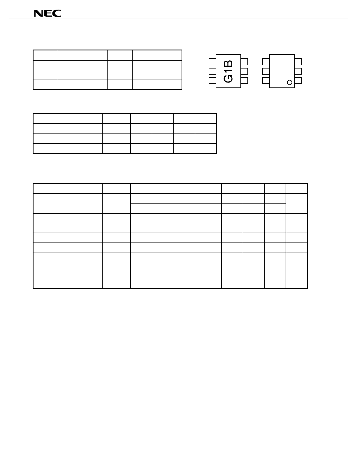
PIN CONNECTION DIAGRAM
PPPP
PG152TA
(Top View)
(Bottom View)
PIN No. CONNECTION PIN No. CONNECTION
1OUT14V
CONT 2
2GND5 IN
3OUT26V
CONT 1
3
2
1
4
5
6
4
5
6
RECOMMENDED OPERATING CONDITIONS (TA = 25 °C)
PARAMETERS SYMBOL MIN. TYP. MAX. UNIT
P
CONT
CONT
in(1 dB)
CONT
+2.7 +3.0 +5.3 V
0.2 0 +0.2 V
ð
in
CONT2
= 3 V, Off chip DC blocking capacitors value; 51 pF)
INS
f = 100 M to 2 GHz 0.6 1.0 dB
+27 +29 dBm
f = 2.5 GHz
Note 1
f = 2.5 GHz
in
f = 100 M to 2 GHz 11 dB
out
f = 100 M to 2 GHz 11 dB
20
f = 1 GHz to 2 GHz 27 30 dBm
sw
CONT
V
= 3 V/0 V RF None 5
CONT1
= 3 V,
Note 1
0.8
30 ns
Control Voltage (OFF) V
Control Voltage (ON) V
Input Power (V
CONT
= 3 V/0 V) P
ELECTRICAL CHARACTERISTICS (Unless otherwise specified, TA = 25 °C, V
CONT2
V
= 0 V or V
CHARACTERISTICS SYMBOL TEST CONDITIONS MIN. TYP. MAX . UNIT
Insertion Loss L
Isolation ISL f = 100 M to 2 GHz 20 22 dB
Input Return Loss RI
Output Return Loss RI
Input Power at 1 dB
Compression Point
Switching Speed t
Control Current I
CONT1
Note 2
= 0 V, V
3
2
1
A
P
Notes 1
2
Characteristic for reference at 2.0 to 2.5 GHz
Pin(1 dB) is measured the input power level when the insertion loss increase more 1 dB than that of
2
linear range. All other characteristics are measured in linear range.
When the
3
PG152TA is used it is necessary to use DC blocking capacitors for No.1 (OUT1), No.3
P
(OUT2) and No.5 (IN). The value of DC blocking capacitors should be chosen to accommodate the
frequency of operation, band width, switching speed and the condition with actual board of your system.
The range of recommended DC blocking capacitor value is less than 100 pF.
The distance between IC’s GND pin and ground pattern of substrate should be as shorter as possible to
4
avoid parasitic parameters.
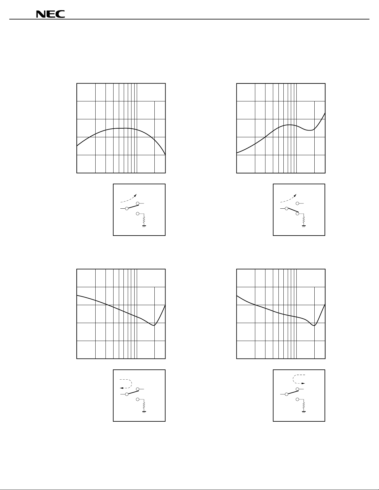
TYPICAL CHARACTERISTICS (TA = 25 °C)
This data is including loss of the test fixture
Note
PPPP
PG152TA
IN-OUT1 INSERTION LOSS vs. FREQUENCY
+2.0
+1.0
V
CONT1
V
CONT2
P
in
= 0 dBm
0
–1.0
- Insertion Loss - dB
INS
L
–2.0
–3.0
100 M 200 M 500 M 1 G 2 G 3 G
f - Frequency - Hz
INS
L
IN
50 Ω
= 0 V
= +3 V
OUT1
OUT2
IN-OUT1 ISOLATION vs. FREQUENCY
0
–10
V
V
P
–20
–30
ISL - Isolation - dB
–40
–50
100 M 200 M 500 M 1 G 2 G 3 G
f - Frequency - Hz
ISL
IN
50 Ω
CONT1
= +3 V
CONT2
= 0 V
in
= 0 dBm
OUT1
OUT2
IN-OUT1 INPUT RETURN LOSS vs. FREQUENCY
+10
0
V
CONT1
V
CONT2
P
in
= 0 dBm
= 0 V
= +3 V
–10
–20
- Input Return Loss - dB
in
–30
RL
–40
100 M 200 M 500 M 1 G 2 G 3 G
f - Frequency - Hz
RL
in
OUT1
IN
50 Ω
OUT2
IN-OUT1 OUTPUT RETURN LOSS vs. FREQUENCY
+10
0
V
CONT1
V
CONT2
P
in
= 0 dBm
= 0 V
= +3 V
–10
–20
- Output Return Loss - dB
–30
out
RL
–40
100 M 200 M 500 M 1 G 2 G 3 G
f - Frequency - Hz
RL
out
OUT1
IN
50 Ω
OUT2
3
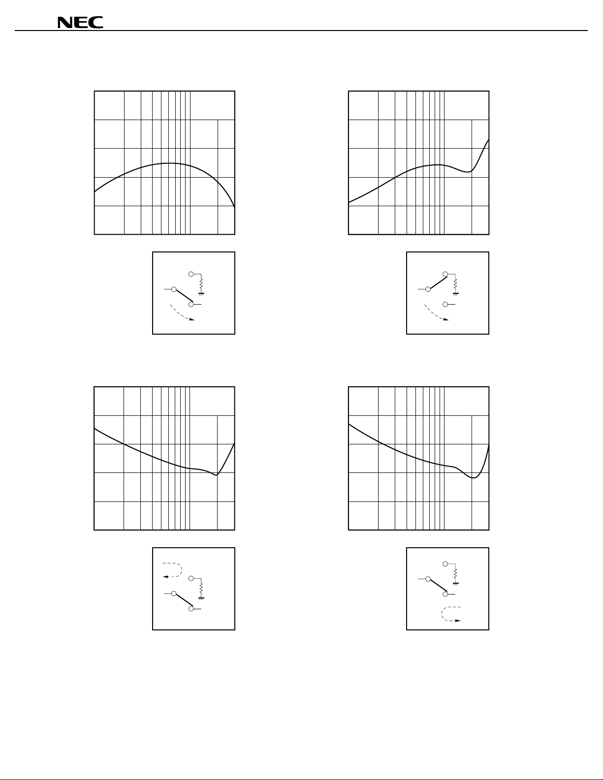
PPPP
PG152TA
IN-OUT2 INSERTION LOSS vs. FREQUENCY
+2.0
+1.0
V
CONT1
V
CONT2
P
in
= 0 dBm
0
–1.0
- Insertion Loss - dB
INS
L
–2.0
–3.0
100 M 200 M 500 M 1 G 2 G 3 G
f - Frequency - Hz
IN
INS
L
= +3 V
= 0 V
OUT1
50 Ω
OUT2
IN-OUT2 ISOLATION vs. FREQUENCY
0
–10
V
V
P
–20
–30
ISL - Isolation - dB
–40
–50
100 M 200 M 500 M 1 G 2 G 3 G
f - Frequency - Hz
IN
ISL
CONT1
= 0 V
CONT2
= +3 V
in
= 0 dBm
OUT1
50 Ω
OUT2
IN-OUT2 INPUT RETURN LOSS vs. FREQUENCY
+10
0
V
CONT1
V
CONT2
P
in
= 0 dBm
= +3 V
= 0 V
–10
–20
- Input Return Loss - dB
in
–30
RL
–40
100 M 200 M 500 M 1 G 2 G 3 G
f - Frequency - Hz
RL
IN
in
OUT1
50 Ω
OUT2
IN-OUT2 OUTPUT RETURN LOSS vs. FREQUENCY
+10
0
V
CONT1
V
CONT2
P
in
= 0 dBm
= +3 V
= 0 V
–10
–20
- Output Return Loss - dB
–30
out
RL
–40
100 M 200 M 500 M 1 G 2 G 3 G
f - Frequency - Hz
OUT1
50 Ω
IN
OUT2
RL
out
4
 Loading...