


Preliminary User’s Manual
PD98502
µ
µ
µµ
Network Controller
Document No. S15543EJ1V0UM00 (1st edition)
Date Published December 2001 NS CP(K)
2001
Printed in Japan

[MEMO]
2
Preliminary User’s Manual S15543EJ1V0UM

SUMMARY OF CONTENTS
CHAPTER 1 INTRODUCTION .................................................................................................................. 23
4120A ...............................................................................................................................57
CHAPTER 2 V
R
CHAPTER 3 SYSTEM CONTROLLER ................................................................................................... 185
CHAPTER 4 ATM CELL PROCESSOR .................................................................................................. 229
CHAPTER 5 ETHERNET CONTROLLER............................................................................................... 277
CHAPTER 6 USB CONTROLLER ..........................................................................................................309
CHAPTER 7 PCI CONTROLLER ............................................................................................................ 370
CHAPTER 8 UART .................................................................................................................................. 414
CHAPTER 9 TIMER ................................................................................................................................. 424
CHAPTER 10 MICRO WIRE.................................................................................................................... 427
APPENDIX A MIPS III INSTRUCTION SET DETAILS............................................................................ 431
APPENDIX B V
4120A COPROCESSOR 0 HAZARDS......................................................................... 590
R
Preliminary User’s Manual S15543EJ1V0UM
3

NOTES FOR CMOS DEVICES
1 PRECAUTION AGAINST ESD FOR SEMICONDUCTORS
Note:
Strong electric field, when exposed to a MOS device, can cause destruction of the gate oxide and
ultimately degrade the device operation. Steps must be taken to stop generation of static electricity
as much as possible, and quickly dissipate it once, when it has occurred. Environmental control
must be adequate. When it is dry, humidifier should be used. It is recommended to avoid using
insulators that easily build static electricity. Semiconductor devices must be stored and transported
in an anti-static container, static shielding bag or conductive material. All test and measurement
tools including work bench and floor should be grounded. The operator should be grounded using
wrist strap. Semiconductor devices must not be touched with bare hands. Similar precautions need
to be taken for PW boards with semiconductor devices on it.
2 HANDLING OF UNUSED INPUT PINS FOR CMOS
Note:
No connection for CMOS device inputs can be cause of malfunction. If no connection is provided
to the input pins, it is possible that an internal input level may be generated due to noise, etc., hence
causing malfunction. CMOS devices behave differently than Bipolar or NMOS devices. Input levels
of CMOS devices must be fixed high or low by using a pull-up or pull-down circuitry. Each unused
DD
pin should be connected to V
being an output pin. All handling related to the unused pins must be judged device by device and
related specifications governing the devices.
or GND with a resistor, if it is considered to have a possibility of
3 STATUS BEFORE INITIALIZATION OF MOS DEVICES
Note:
Power-on does not necessarily define initial status of MOS device. Production process of MOS
does not define the initial operation status of the device. Immediately after the power source is
turned ON, the devices with reset function have not yet been initialized. Hence, power-on does
not guarantee out-pin levels, I/O settings or contents of registers. Device is not initialized until the
reset signal is received. Reset operation must be executed immediately after power-on for devices
having reset function.
4
Preliminary User’s Manual S15543EJ1V0UM

VR4100, VR4102, VR4111, VR4120A, VR4300, VR4305, VR4310, VR4400, VR5000, VR10000, VR Series, VR4000
Series, V
R4100 Series, and EEPROM are trademarks of NEC Corporation.
Micro Wire is a trademark of National Semiconductor Corp.
iAPX is a trademark of Intel Corp.
DEC VAX is a trademark of Digital Equipment Corp.
UNIX is a registered trademark in the United States and other countries, licensed exclusively through
X/Open Company, Ltd.
Ethernet is a trademark of Xerox Corp.
MIPS is a trademark of MIPS Technologies, Inc.
• The information contained in this document is being issued in advance of the production cycle for the
device. The parameters for the device may change before final production or NEC Corporation, at its own
discretion, may withdraw the device prior to its production.
• Not all devices/types available in every country. Please check with local NEC representative for availability
and additional information.
• No part of this document may be copied or reproduced in any form or by any means without the prior written
consent of NEC Corporation. NEC Corporation assumes no responsibility for any errors which may appear in
this document.
• NEC Corporation does not assume any liability for infringement of patents, copyrights or other intellectual property
rights of third parties by or arising from use of a device described herein or any other liability arising from use
of such device. No license, either express, implied or otherwise, is granted under any patents, copyrights or other
intellectual property rights of NEC Corporation or others.
• Descriptions of circuits, software, and other related information in this document are provided for illustrative
purposes in semiconductor product operation and application examples. The incorporation of these circuits,
software, and information in the design of the customer's equipment shall be done under the full responsibility
of the customer. NEC Corporation assumes no responsibility for any losses incurred by the customer or third
parties arising from the use of these circuits, software, and information.
• While NEC Corporation has been making continuous effort to enhance the reliability of its semiconductor devices,
the possibility of defects cannot be eliminated entirely. To minimize risks of damage or injury to persons or
property arising from a defect in an NEC semiconductor device, customers must incorporate sufficient safety
measures in its design, such as redundancy, fire-containment, and anti-failure features.
• NEC devices are classified into the following three quality grades:
"Standard", "Special", and "Specific". The Specific quality grade applies only to devices developed based on a
customer designated "quality assurance program" for a specific application. The recommended applications of
a device depend on its quality grade, as indicated below. Customers must check the quality grade of each device
before using it in a particular application.
Standard: Computers, office equipment, communications equipment, test and measurement equipment,
audio and visual equipment, home electronic appliances, machine tools, personal electronic
equipment and industrial robots
Special: Transportation equipment (automobiles, trains, ships, etc.), traffic control systems, anti-disaster
systems, anti-crime systems, safety equipment and medical equipment (not specifically designed
for life support)
Specific: Aircraft, aerospace equipment, submersible repeaters, nuclear reactor control systems, life
support systems or medical equipment for life support, etc.
The quality grade of NEC devices is "Standard" unless otherwise specified in NEC's Data Sheets or Data Books.
If customers intend to use NEC devices for applications other than those specified for Standard quality grade,
they should contact an NEC sales representative in advance.
Preliminary User’s Manual S15543EJ1V0UM
M5D 98. 12
5

PREFACE
Readers This manual is intended for engineers who need to be familiar with the capability of
PD98502 in order to develop application systems based on it.
µ
the
Purpose The purpose of this manual is to help users understand the hardware capabilities
(listed below) of the
Configuration This manual consists of the following chapters:
• Introduction
4120A CPU
• VR
• System controller
• ATM cell processor
• Ethernet controller
• USB controller
• PCI controller
• UART
• Timer
• Micro Wire
PD98502.
µ
Guidance Readers of this manual should already have a general knowledge of electronics, logic
circuits, and microcomputers.
PD98502:
To gain an overall understanding of the function of the
→ Read through all the chapters, in sequence.
To check the electrical characteristics of the
→ Refer to the separate data sheet.
Notation This manual uses the following conventions:
Data bit significance: High-order bits on the left side;
low-order bits on the right side
Active low: XXXX_B (Pin and signal names are suffixed with _B.)
Note: Explanation of an indicated part of text
Caution: Information requiring the user’s special attention
Remark: Supplementary information
Numerical value: Binary ... xxxx or xxxxB
Decimal ... xxxx
Hexadecimal ... xxxxH
Related Document Use this manual in combination with the following document.
The related documents indicated in this publication may include preliminary versions.
However, preliminary versions are not marked as such.
PD98502:
µ
µ
PD98502 Data Sheet: S15409E
µ
•
6
Preliminary User’s Manual S15543EJ1V0UM

CONTENTS
CHAPTER 1 INTRODUCTION ...............................................................................................................23
1.1 Features ......................................................................................................................................23
1.2 Ordering Information ................................................................................................................. 23
1.3 System Configuration................................................................................................................ 24
1.4 Block Diagram (Summary) ........................................................................................................ 25
1.5 Block Diagram (Detail)............................................................................................................... 26
1.5.1 VR4120A RISC processor core...................................................................................................... 26
1.5.2 IBUS ..............................................................................................................................................27
1.5.3 System controller...........................................................................................................................28
1.5.4 ATM cell processor........................................................................................................................29
1.5.5 Ethernet controller .........................................................................................................................30
1.5.6 USB controller ...............................................................................................................................31
1.5.7 PCI controller.................................................................................................................................32
1.6 Pin Configuration (Bottom View) .............................................................................................33
1.7 Pin Function ...............................................................................................................................37
1.7.1 Power supply .................................................................................................................................37
1.7.2 System PLL power supply .............................................................................................................37
1.7.3 USB PLL power supply..................................................................................................................37
1.7.4 System control interface ................................................................................................................38
1.7.5 Memory interface...........................................................................................................................39
1.7.6 PCI interface..................................................................................................................................41
1.7.7 ATM interface ................................................................................................................................43
1.7.8 Ethernet interface ..........................................................................................................................45
1.7.9 USB interface ................................................................................................................................46
1.7.10 UART interface ..............................................................................................................................47
1.7.11 Micro Wire interface.......................................................................................................................47
1.7.12 Parallel port interface.....................................................................................................................47
1.7.13 Boundary scan interface................................................................................................................47
1.7.14 I.C. – open .....................................................................................................................................48
1.7.15 I.C.– pull down...............................................................................................................................48
1.7.16 I.C. – pull down with resistor..........................................................................................................48
1.7.17 I.C. – pull up ..................................................................................................................................48
1.8 I/O Register Map......................................................................................................................... 49
1.9 Memory Map ............................................................................................................................... 53
1.10 Reset Configuration................................................................................................................... 54
1.11 Interrupts .................................................................................................................................... 55
1.12 Clock Control Unit .....................................................................................................................56
CHAPTER 2 V
2.1 Overview for V
2.1.1 Internal block configuration............................................................................................................58
2.1.2 VR
2.1.3 VR4120A instruction set overview..................................................................................................60
2.1.4 Data formats and addressing.........................................................................................................61
2.1.5 Coprocessors (CP0) ...................................................................................................................... 63
4120A ............................................................................................................................ 57
R
4120A ...............................................................................................................57
R
4120A registers .........................................................................................................................59
Preliminary User’s Manual S15543EJ1V0UM
7

2.1.6 Floating-point unit (FPU)................................................................................................................64
2.1.7 CPU core memory management system (MMU) ...........................................................................65
2.1.8 Translation lookaside buffer (TLB).................................................................................................65
2.1.9 Operating modes ...........................................................................................................................65
2.1.10 Cache ............................................................................................................................................65
2.1.11 Instruction pipeline.........................................................................................................................66
2.2 MIPS III Instruction Set Summary.............................................................................................66
2.2.1 MIPS III ISA instruction formats.....................................................................................................66
2.2.2 Instruction classes .........................................................................................................................67
2.3 Pipeline........................................................................................................................................84
2.3.1 Pipeline stages ..............................................................................................................................84
2.3.2 Branch delay..................................................................................................................................87
2.3.3 Load delay .....................................................................................................................................87
2.3.4 Pipeline operation ..........................................................................................................................88
2.3.5 Interlock and exception handling ...................................................................................................94
2.3.6 Program compatibility ..................................................................................................................100
2.4 Memory Management System ................................................................................................101
2.1.1 Translation lookaside buffer (TLB)..............................................................................................101
2.1.2 Virtual address space ..................................................................................................................102
2.1.3 Physical address space ...............................................................................................................116
2.1.4 System control coprocessor.........................................................................................................117
2.1.5 CP0 registers ...............................................................................................................................119
2.5 Exception Processing.............................................................................................................129
2.5.1 Exception processing operation...................................................................................................129
2.5.2 Precision of exceptions................................................................................................................130
2.5.3 Exception processing registers ....................................................................................................130
2.1.4 Details of exceptions....................................................................................................................142
2.1.5 Exception processing and servicing flowcharts............................................................................158
2.2 Initialization Interface ..............................................................................................................165
2.2.1 Cold reset ....................................................................................................................................165
2.2.2 Soft reset .....................................................................................................................................165
2.2.3 VR4120A processor modes..........................................................................................................165
2.3 Cache Memory..........................................................................................................................168
2.3.1 Memory organization ...................................................................................................................168
2.3.2 Cache organization......................................................................................................................169
2.3.3 Cache operations.........................................................................................................................171
2.3.4 Cache states................................................................................................................................172
2.3.5 Cache state transition diagrams ..................................................................................................173
2.3.6 Cache data integrity.....................................................................................................................174
2.3.7 Manipulation of the caches by an external agent.........................................................................181
2.4 CPU Core Interrupts.................................................................................................................182
2.4.1 Non-maskable interrupt (NMI)......................................................................................................182
2.4.2 Ordinary interrupts .......................................................................................................................182
2.4.3 Software interrupts generated in CPU core .................................................................................182
2.4.4 Timer interrupt .............................................................................................................................182
2.4.5 Asserting interrupts......................................................................................................................183
8
Preliminary User’s Manual S15543EJ1V0UM

CHAPTER 3 SYSTEM CONTROLLER ............................................................................................... 185
3.1 Overview ...................................................................................................................................185
3.1.1 CPU interface ..............................................................................................................................185
3.1.2 Memory interface.........................................................................................................................185
3.1.3 IBUS Interface .............................................................................................................................185
3.1.4 UART...........................................................................................................................................186
3.1.5 EEPROM .....................................................................................................................................186
3.1.6 Timer ...........................................................................................................................................186
3.1.7 Interrupt controller .......................................................................................................................186
3.1.8 DSU (Deadman’s SW Unit) .........................................................................................................186
3.1.9 System block diagram ................................................................................................................. 187
3.1.10 Data flow diagram........................................................................................................................188
3.2 Registers................................................................................................................................... 189
3.2.1 Register map ...............................................................................................................................189
3.2.2 S_GMR (General Mode Register) ...............................................................................................191
3.2.3 S_GSR (General Status Register)...............................................................................................191
3.2.4 S_ISR (Interrupt Status Register)................................................................................................192
3.2.5 S_IMR (Interrupt Mask Register).................................................................................................193
3.2.6 S_NSR (NMI Status Register) ..................................................................................................... 194
3.2.7 S_NER (NMI Enable Register) ....................................................................................................195
3.2.8 S_VER (Version Register)...........................................................................................................195
3.2.9 S_IOR (IO Port Register).............................................................................................................196
3.2.10 S_WRCR (Warm Reset Control Register)...................................................................................197
3.2.11 S_WRSR (Warm Reset Status Register).....................................................................................198
3.2.12 S_PWCR (Power Control Register).............................................................................................199
3.2.13 S_PWSR (Power Status Register) ..............................................................................................200
3.3 CPU Interface ........................................................................................................................... 201
3.3.1 Overview......................................................................................................................................201
3.3.2 Data rate control ..........................................................................................................................201
3.3.3 Burst size control ......................................................................................................................... 201
3.3.4 Address decoding........................................................................................................................201
3.3.5 Endian conversion .......................................................................................................................201
3.3.6 I/O performance...........................................................................................................................203
3.4 Memory Interface ..................................................................................................................... 204
3.4.1 Overview......................................................................................................................................204
3.4.2 Memory regions...........................................................................................................................204
3.4.3 Memory signal connections.........................................................................................................205
3.4.4 Memory performance...................................................................................................................206
3.4.5 RMMDR (ROM Mode Register)................................................................................................... 207
3.4.6 RMATR (ROM Access Timing Register)......................................................................................207
3.4.7 SDMDR (SDRAM Mode Register)...............................................................................................209
3.4.8 SDTSR (SDRAM Type Selection Register) .................................................................................210
3.4.9 SDPTR (SDRAM Precharge Timing Register).............................................................................211
3.4.10 SDRMR (SDRAM Refresh Mode Register) .................................................................................211
3.4.11 SDRCR (SDRAM Refresh Timer Count Register) .......................................................................212
3.4.12 MBCR (Memory Bus Control Register)........................................................................................212
3.4.13 Boot ROM....................................................................................................................................213
3.4.14 SDRAM........................................................................................................................................216
Preliminary User’s Manual S15543EJ1V0UM
9

3.4.15 SDRAM refresh............................................................................................................................219
3.4.16 Memory-to-CPU prefetch FIFO....................................................................................................219
3.4.17 CPU-to-memory write FIFO .........................................................................................................219
3.4.18 SDRAM memory initialization ......................................................................................................220
3.5 IBUS Interface...........................................................................................................................221
3.5.1 Overview......................................................................................................................................221
3.5.2 Endian Conversion on IBUS master ............................................................................................221
3.5.3 Endian Conversion on IBUS slave...............................................................................................222
3.5.4 ITCNTR (IBUS Timeout Timer Control Register).........................................................................223
3.5.5 ITSETR (IBUS Timeout Timer Set Register)................................................................................223
3.6 DSU (Deadman’s SW Unit) ......................................................................................................224
3.6.1 Overview......................................................................................................................................224
3.6.2 DSUCNTR (DSU Control Register)..............................................................................................224
3.6.3 DSUSETR (DSU Time Set Register) ...........................................................................................224
3.6.4 DSUCLRR (DSU Clear Register).................................................................................................224
3.6.5 DSUTIMR (DSU Elapsed Time Register) ....................................................................................225
3.6.6 DSU register setting flow .............................................................................................................225
3.7 Endian Mode Software Issues ................................................................................................226
3.7.1 Overview......................................................................................................................................226
3.7.2 Endian modes..............................................................................................................................226
CHAPTER 4 ATM CELL PROCESSOR.............................................................................................229
4.1 Overview ...................................................................................................................................229
4.1.1 Function features .........................................................................................................................229
4.1.2 Block diagram of ATM cell processor...........................................................................................230
4.1.3 ATM cell processing operation overview......................................................................................232
4.2 Memory Space..........................................................................................................................236
4.2.1 Work RAM and register space.....................................................................................................237
4.2.2 Shared memory ...........................................................................................................................237
4.3 Interruption ...............................................................................................................................237
4.4 Registers for ATM Cell Processing ........................................................................................238
4.4.1 Register map ...............................................................................................................................238
4.4.2 A_GMR (General Mode Register)................................................................................................240
4.4.3 A_GSR (General Status Register)...............................................................................................240
4.4.4 A_IMR (Interrupt Mask Register) .................................................................................................241
4.4.5 A_RQU (Receiving Queue Underrun Register) ...........................................................................242
4.4.6 A_RQA (Receiving Queue Alert Register)...................................................................................242
4.4.7 A_VER (Version Register) ...........................................................................................................242
4.4.8 A_CMR (Command Register)......................................................................................................242
4.4.9 A_CER (Command Extension Register)......................................................................................242
4.4.10 A_MSA0 to A_MSA3 (Mailbox Start Address Register)...............................................................243
4.4.11 A_MBA0 to A_MBA3 (Mailbox Bottom Address Register) ...........................................................243
4.4.12 A_MTA0 to A_MTA3 (Mailbox Tail Address Register) .................................................................243
4.4.13 A_MWA0 to A_MWA3 (Mailbox Write Address Register) ............................................................244
4.4.14 A_RCC (Valid Received Cell Counter).........................................................................................244
4.4.15 A_TCC (Valid Transmitted Cell Counter).....................................................................................244
4.4.16 A_RUEC (Receive Unprovisioned VPI/VCI Error Cell Counter)...................................................244
4.4.17 A_RIDC (Receive Internal Dropped Cell Counter).......................................................................244
10
Preliminary User’s Manual S15543EJ1V0UM

4.4.18 A_T1R (T1 Time Register)...........................................................................................................245
4.4.19 A_TSR (Time Stamp Register)....................................................................................................245
4.4.20 A_IBBAR (IBUS Base Address Register) ....................................................................................245
4.4.21 A_INBAR (Instruction Base Address Register)............................................................................245
4.4.22 A_UMCMD (UTOPIA Management Interface Command Register) .............................................246
4.5 Data Structure .......................................................................................................................... 247
4.5.1 Tx buffer structure .......................................................................................................................247
4.5.2 Rx pool structure .........................................................................................................................250
4.6 Initialization .............................................................................................................................. 255
4.6.1 Before starting RISC core............................................................................................................255
4.6.2 After RISC core’s F/W is starting.................................................................................................256
4.7 Commands ............................................................................................................................... 257
4.7.1 Set_Link_Rate command ............................................................................................................258
4.7.2 Open_Channel command............................................................................................................258
4.7.3 Close_Channel command ...........................................................................................................259
4.7.4 Tx_Ready command....................................................................................................................260
4.7.5 Add_Buffers command ................................................................................................................261
4.7.6 Indirect_Access command...........................................................................................................262
4.8 Operations ................................................................................................................................ 262
4.8.1 Work RAM usage ........................................................................................................................262
4.8.2 Transmission function..................................................................................................................263
4.8.3 Receiving function .......................................................................................................................270
4.8.4 Mailbox ........................................................................................................................................ 276
CHAPTER 5 ETHERNET CONTROLLER ..........................................................................................277
5.1 Overview ...................................................................................................................................277
5.1.1 Features ......................................................................................................................................277
5.1.2 Block diagram of Ethernet controller block ..................................................................................277
5.2 Registers................................................................................................................................... 279
5.2.1 Register map ...............................................................................................................................279
5.2.2 En_MACC1 (MAC Configuration Register 1)...............................................................................285
5.2.3 En_MACC2 (MAC Configuration Register 2)...............................................................................286
5.2.4 En_IPGT (Back-to-Back IPG Register)........................................................................................286
5.2.5 En_IPGR (Non Back-to-Back IPG Register)................................................................................286
5.2.6 En_CLRT (Collision Register)......................................................................................................287
5.2.7 En_LMAX (Maximum Packet Length Register) ...........................................................................287
5.2.8 En_RETX (Retry Count Register)................................................................................................ 287
5.2.9 En_LSA2 (Station Address Register 2)........................................................................................287
5.2.10 En_LSA1 (Station Address Register 1)........................................................................................287
5.2.11 En_PTVR (Pause Timer Value Read Register)........................................................................... 288
5.2.12 En_VLTP (VLAN Type Register) ................................................................................................. 288
5.2.13 En_MIIC (MII Configuration Register)..........................................................................................288
5.2.14 En_MCMD (MII Command Register)........................................................................................... 288
5.2.15 En_MADR (MII Address Register)...............................................................................................289
5.2.16 En_MWTD (MII Write Data Register)...........................................................................................289
5.2.17 En_MRDD (MII Read Data Register)...........................................................................................289
5.2.18 En_MIND (MII Indicate Register).................................................................................................289
5.2.19 En_AFR (Address Filtering Register)...........................................................................................290
Preliminary User’s Manual S15543EJ1V0UM
11

5.2.20 En_HT1 (Hash Table Register 1).................................................................................................290
5.2.21 En_HT2 (Hash Table Register 2).................................................................................................290
5.2.22 En_CAR1 (Carry Register 1) .......................................................................................................291
5.2.23 En_CAR2 (Carry Register 2) .......................................................................................................292
5.2.24 En_CAM1 (Carry Register 1 Mask Register) ...............................................................................293
5.2.25 En_CAM2 (Carry Register 2 Mask Register) ...............................................................................294
5.2.26 En_TXCR (Transmit Configuration Register)...............................................................................294
5.2.27 En_TXFCR (Transmit FIFO Control Register) .............................................................................295
5.2.28 En_TXDPR (Transmit Descriptor Pointer) ...................................................................................296
5.2.29 En_RXCR (Receive Configuration Register) ...............................................................................296
5.2.30 En_RXFCR (Receive FIFO Control Register)..............................................................................297
5.2.31 En_RXDPR (Receive Descriptor Pointer)....................................................................................297
5.2.32 En_RXPDR (Receive Pool Descriptor Pointer)............................................................................298
5.2.33 En_CCR (Configuration Register)................................................................................................298
5.2.34 En_ISR (Interrupt Serves Register) .............................................................................................298
5.2.35 En_MSR (Mask Serves Register)................................................................................................299
5.3 Operation ..................................................................................................................................300
5.3.1 Initialization..................................................................................................................................300
5.3.2 Buffer structure for Ethernet Controller block...............................................................................300
5.3.3 Buffer descriptor format ...............................................................................................................301
5.3.4 Frame transmission .....................................................................................................................302
5.3.5 Frame reception...........................................................................................................................305
5.3.6 Address Filtering..........................................................................................................................307
CHAPTER 6 USB CONTROLLER ......................................................................................................309
6.1 Overview ...................................................................................................................................309
6.1.1 Features.......................................................................................................................................309
6.1.2 Internal block diagram..................................................................................................................310
6.2 Registers ...................................................................................................................................311
6.2.1 Register map ...............................................................................................................................311
6.2.2 U_GMR (USB General Mode Register) .......................................................................................313
6.2.3 U_VER (USB Frame Number/Version Register)..........................................................................313
6.2.4 U_GSR1 (USB General Status Register 1)..................................................................................314
6.2.5 U_IMR1 (USB Interrupt Mask Register 1)....................................................................................316
6.2.6 U_GSR2 (USB General Status Register 2)..................................................................................318
6.2.7 U_IMR2 (USB Interrupt Mask Register 2)....................................................................................319
6.2.8 U_EP0CR (USB EP0 Control Register).......................................................................................320
6.2.9 U_EP1CR (USB EP1 Control Register).......................................................................................321
6.2.10 U_EP2CR (USB EP2 Control Register).......................................................................................321
6.2.11 U_EP3CR (USB EP3 Control Register).......................................................................................322
6.2.12 U_EP4CR (USB EP4 Control Register).......................................................................................323
6.2.13 U_EP5CR (USB EP5 Control Register).......................................................................................324
6.2.14 U_EP6CR (USB EP6 Control Register).......................................................................................324
6.2.15 U_CMR (USB Command Register)..............................................................................................325
6.2.16 U_CA (USB Command Extension Register)................................................................................325
6.2.17 U_TEPSR (USB Tx EndPoint Status Register)............................................................................326
6.2.18 U_RP0IR (USB Rx Pool0 Information Register) ..........................................................................326
6.2.19 U_RP0AR (USB Rx Pool0 Address Register)..............................................................................327
12
Preliminary User’s Manual S15543EJ1V0UM

6.2.20 U_RP1IR (USB Rx Pool1 Information Register)..........................................................................327
6.2.21 U_RP1AR (USB Rx Pool1 Address Register) .............................................................................327
6.2.22 U_RP2IR (USB Rx Pool2 Information Register)..........................................................................328
6.2.23 U_RP2AR (USB Rx Pool2 Address Register) .............................................................................328
6.2.24 U_TMSA (USB Tx MailBox Start Address Register)....................................................................328
6.2.25 U_TMBA (USB Tx MailBox Bottom Address Register)................................................................328
6.2.26 U_TMRA (USB Tx MailBox Read Address Register)...................................................................328
6.2.27 U_TMWA (USB Tx MailBox Write Address Register)..................................................................329
6.2.28 U_RMSA (USB Rx MailBox Start Address Register)...................................................................329
6.2.29 U_RMBA (USB Rx MailBox Bottom Address Register)...............................................................329
6.2.30 U_RMRA (USB Rx MailBox Read Address Register).................................................................. 329
6.2.31 U_RMWA (USB Rx MailBox Write Address Register) ................................................................. 329
6.3 USB Attachment Sequence .................................................................................................... 330
6.4 Initialization .............................................................................................................................. 331
6.4.1 Receive pool settings...................................................................................................................332
6.4.2 Transmit/receive MailBox settings...............................................................................................332
6.5 Data Transmit Function...........................................................................................................334
6.5.1 Overview of transmit processing..................................................................................................334
6.5.2 Tx buffer configuration.................................................................................................................334
6.5.3 Data transmit modes....................................................................................................................337
6.5.4 VR
6.5.5 USB controller processing at data transmitting............................................................................341
6.5.6 Tx indication ................................................................................................................................343
4120A processing at data transmitting ....................................................................................338
6.6 Data Receive Function ............................................................................................................344
6.6.1 Overview of receive processing...................................................................................................344
6.6.2 Rx Buffer configuration ................................................................................................................345
6.6.3 Receive pool settings...................................................................................................................347
6.6.4 Data receive mode.......................................................................................................................348
6.6.5 VR
6.6.6 USB controller receive processing...............................................................................................352
6.6.7 Detection of errors on USB..........................................................................................................358
6.6.8 Rx data corruption on Isochronous EndPoint ..............................................................................360
6.6.9 Rx FIFO overrun..........................................................................................................................361
6.6.10 Rx indication ................................................................................................................................362
4120A receive processing .......................................................................................................351
6.7 Power Management .................................................................................................................364
6.7.1 Suspend ......................................................................................................................................364
6.7.2 Resume ....................................................................................................................................... 365
6.7.3 Remote wake up..........................................................................................................................366
6.8 Receiving SOF Packet ............................................................................................................. 367
6.8.1 Receiving SOF Packet and updating the Frame Number............................................................ 367
6.8.2 Updating Frame Number automatically .......................................................................................367
6.8.3 Checking if the skew of SOF arrival time is allowable of not........................................................367
6.9 Loopback Mode........................................................................................................................ 368
6.10 Example of Connection ........................................................................................................... 369
Preliminary User’s Manual S15543EJ1V0UM
13

CHAPTER 7 PCI CONTROLLER .........................................................................................................370
7.1 Overview ...................................................................................................................................370
7.2 Bus Bridge Functions..............................................................................................................371
7.2.1 Internal bus to PCI transaction.....................................................................................................371
7.2.2 PCI to internal bus transaction.....................................................................................................376
7.2.3 Abnormal Termination..................................................................................................................381
7.2.4 Warning for Deadlocks.................................................................................................................382
7.3 PCI Power Management Interface ..........................................................................................383
7.3.1 Power state..................................................................................................................................383
7.3.2 Power management event...........................................................................................................383
7.3.3 Power supply ...............................................................................................................................383
7.3.4 Power state transition ..................................................................................................................384
7.4 Functions in Host-mode ..........................................................................................................386
7.4.1 Generating configuration cycle ....................................................................................................386
7.4.2 PCI bus arbiter .............................................................................................................................388
7.4.3 Reset output ................................................................................................................................389
7.4.4 Interrupt input...............................................................................................................................389
7.5 Registers ...................................................................................................................................390
7.5.1 Register map ...............................................................................................................................390
7.5.2 P_PLBA (PCI Lower Base Address Register)..............................................................................391
7.5.3 P_IBBA (Internal Bus Base Address Register) ............................................................................391
7.5.4 P_VERR (Version Register).........................................................................................................391
7.5.5 P_PCAR (PCI Configuration Address Register) ..........................................................................392
7.5.6 P_PCDR (PCI Configuration Data Register)................................................................................392
7.5.7 P_IGSR (Internal Bus-side General Status Register) ..................................................................393
7.5.8 P_IIMR (Internal Bus Interrupt Mask Register) ............................................................................394
7.5.9 P_PGSR (PCI-side General Status Register)..............................................................................395
7.5.10 P_IIMR (Internal Bus Interrupt Mask Register) ............................................................................396
7.5.11 P_PIMR (PCI Interrupt Mask Register)........................................................................................397
7.5.12 P_HMCR (Host Mode Control Register) ......................................................................................398
7.5.13 P_PCDR (Power Consumption Data Register)............................................................................398
7.5.14 P_PDDR (Power Dissipation Data Register) ...............................................................................398
7.5.15 P_BCNT (Bridge Control Register) ..............................................................................................399
7.5.16 P_PPCR (PCI Power Control Register) .......................................................................................400
7.5.17 P_SWRR (Software Reset Register) ...........................................................................................400
7.5.18 P_RTMR (Retry Timer Register)..................................................................................................401
7.5.19 P_CONFIG (PCI Configuration Registers)...................................................................................401
7.2 Information for Software .........................................................................................................411
7.2.1 NIC mode.....................................................................................................................................411
7.2.2 Host mode ...................................................................................................................................412
CHAPTER 8 UART ...............................................................................................................................414
8.1 Overview ...................................................................................................................................414
8.2 UART Block Diagram ...............................................................................................................414
8.3 Registers ...................................................................................................................................415
8.3.1 Register map ...............................................................................................................................415
8.3.2 UARTRBR (UART Receiver data Buffer Register).......................................................................416
8.3.3 UARTTHR (UART Transmitter data Holding Register)................................................................416
14
Preliminary User’s Manual S15543EJ1V0UM

8.3.4 UARTIER (UART Interrupt Enable Register)...............................................................................416
8.3.5 UARTDLL (UART Divisor Latch LSB Register) ...........................................................................416
8.3.6 UARTDLM (UART Divisor Latch MSB Register) .........................................................................417
8.3.7 UARTIIR (UART Interrupt ID Register)........................................................................................418
8.3.8 UARTFCR (UART FIFO Control Register) ..................................................................................419
8.3.9 UARTLCR (UART Line Control Register)....................................................................................420
8.3.10 UARTMCR (UART Modem Control Register)..............................................................................421
8.3.11 UARTLSR (UART Line Status Register)......................................................................................422
8.3.12 UARTMSR (UART Modem Status Register) ...............................................................................423
8.3.13 UARTSCR (UART Scratch Register)...........................................................................................423
CHAPTER 9 TIMER.............................................................................................................................. 424
9.1 Overview ...................................................................................................................................424
9.2 Block Diagram.......................................................................................................................... 424
9.3 Registers................................................................................................................................... 425
9.3.1 Register map ...............................................................................................................................425
9.3.2 TMMR (Timer Mode Register).....................................................................................................425
9.3.3 TM0CSR (Timer CH0 Count Set Register)..................................................................................426
9.3.4 TM1CSR (Timer CH1 Count Set Register)..................................................................................426
9.3.5 TM0CCR (Timer CH0 Current Count Register) ...........................................................................426
9.3.6 TM1CCR (Timer CH1 Current Count Register) ...........................................................................426
CHAPTER 10 MICRO WIRE ................................................................................................................. 427
10.1 Overview ...................................................................................................................................427
10.2 Operations ................................................................................................................................ 428
10.2.1 Data read at the power up load ...................................................................................................428
10.2.2 Accessing to EEPROM................................................................................................................ 428
10.3 Registers................................................................................................................................... 429
10.3.1 Register map ...............................................................................................................................429
10.3.2 ECCR (EEPROM Command Control Register) ........................................................................... 429
10.3.3 ERDR (EEPROM Read Data Register) .......................................................................................429
10.3.4 MACAR1 (MAC Address Register 1)........................................................................................... 429
10.3.5 MACAR2 (MAC Address Register 2)........................................................................................... 429
10.3.6 MACAR3 (MAC Address Register 3)........................................................................................... 430
APPENDIX A MIPS III INSTRUCTION SET DETAILS...................................................................... 431
A.1 Instruction Notation Conventions ........................................................................................ 431
A.2 Load and Store Instructions ................................................................................................433
A.3 Jump and Branch Instructions ............................................................................................ 434
A.4 System Control Coprocessor (CP0) Instructions............................................................. 435
A.5 CPU Instruction ....................................................................................................................... 435
A.6 CPU Instruction Opcode Bit Encoding.............................................................................. 588
APPENDIX B V
4120A COPROCESSOR 0 HAZARDS.................................................................... 590
R
Preliminary User’s Manual S15543EJ1V0UM
15

LIST OF FIGURES (1/5)
Figure No. Title Page
1-1 Examples of the µPD98502 System Configuration ........................................................................................24
1-2 Block Diagram of the µPD98502....................................................................................................................25
1-3 Block Diagram of VR4120A RISC Processor..................................................................................................26
1-4 Block Diagram of IBUS ..................................................................................................................................27
1-5 Block Diagram of System Controller ..............................................................................................................28
1-6 Block Diagram of ATM Cell Processor...........................................................................................................29
1-7 Block Diagram of Ethernet Controller.............................................................................................................30
1-8 Block Diagram of USB Controller...................................................................................................................31
1-9 Block Diagram of PCI Bus controller..............................................................................................................32
1-10 Memory Map..................................................................................................................................................53
1-11 Reset Configuration .......................................................................................................................................54
1-12 Interrupt Signal Connection............................................................................................................................55
1-13 Block Diagram of Clock Control Unit..............................................................................................................56
4120A Core Internal Block Diagram...........................................................................................................57
2-1 V
2-2 VR
2-3 CPU Instruction Formats (32-bit Length Instruction)......................................................................................60
2-4 Little-Endian Byte Ordering in Word Data ......................................................................................................61
2-5 Little-Endian Byte Ordering in Double Word Data..........................................................................................61
2-6 Misaligned Word Accessing (Little-Endian)....................................................................................................62
2-7 CP0 Registers................................................................................................................................................63
2-8 MIPS III ISA CPU Instruction Formats ...........................................................................................................66
2-9 Pipeline Stages (MIPS III Instruction Mode)...................................................................................................84
2-10 Instruction Execution in the Pipeline ..............................................................................................................85
2-11 Pipeline Activities (MIPS III)...........................................................................................................................85
2-12 Branch Delay (In MIPS III Instruction Mode)..................................................................................................87
2-13 ADD Instruction Pipeline Activities (In MIPS III Instruction Mode)..................................................................88
2-14 JALR Instruction Pipeline Activities (In MIPS III Instruction Mode) ................................................................89
2-15 BEQ Instruction Pipeline Activities (In MIPS III Instruction Mode)..................................................................90
2-16 TLT Instruction Pipeline Activities ..................................................................................................................91
2-17 LW Instruction Pipeline Activities (In MIPS III Instruction Mode)....................................................................92
2-18 SW Instruction Pipeline Activities (In MIPS III Instruction Mode) ...................................................................93
2-19 Relationship among Interlocks, Exceptions, and Faults.................................................................................94
2-20 Exception Detection.......................................................................................................................................96
2-21 Data Cache Miss Stall....................................................................................................................................97
2-22 CACHE Instruction Stall.................................................................................................................................97
2-23 Load Data Interlock........................................................................................................................................98
2-24 MD Busy Interlock..........................................................................................................................................99
2-25 Virtual-to-Physical Address Translation .......................................................................................................102
2-26 32-bit Mode Virtual Address Translation ......................................................................................................104
2-27 64-bit Mode Virtual Address Translation ......................................................................................................105
2-28 User Mode Address Space..........................................................................................................................106
R
4120A Registers ........................................................................................................................................59
16
Preliminary User’s Manual S15543EJ1V0UM

LIST OF FIGURES (2/5)
Figure No. Title Page
2-29 Supervisor Mode Address Space ................................................................................................................108
2-30 Kernel Mode Address Space.......................................................................................................................111
2-31
2-32 CP0 Registers and TLB...............................................................................................................................117
2-33 Format of a TLB Entry .................................................................................................................................118
2-34 Index Register..............................................................................................................................................119
2-35 Random Register.........................................................................................................................................119
2-36 EntryLo0 and EntryLo1 Registers................................................................................................................120
2-37 Page Mask Register ....................................................................................................................................121
2-38 Positions Indicated by Wired Register ......................................................................................................... 122
2-39 Wired Register.............................................................................................................................................122
2-40 EntryHi Register...........................................................................................................................................123
2-41 PRId Register ..............................................................................................................................................123
2-42 Config Register Format................................................................................................................................124
2-43 LLAddr Register...........................................................................................................................................125
2-44 TagLo Register ............................................................................................................................................125
2-45 TagHi Register.............................................................................................................................................125
2-46 TLB Address Translation .............................................................................................................................127
2-47 Context Register Format..............................................................................................................................131
2-48 BadVAddr Register Format..........................................................................................................................132
2-49 Count Register Format ................................................................................................................................132
2-50 Compare Register Format ........................................................................................................................... 133
2-51 Status Register Format................................................................................................................................134
2-52 Status Register Diagnostic Status Field.......................................................................................................135
2-53 Cause Register Format................................................................................................................................136
2-54 EPC Register Format...................................................................................................................................138
2-55 WatchLo Register Format............................................................................................................................ 139
2-56 WatchHi Register Format ............................................................................................................................139
2-57 XContext Register Format ...........................................................................................................................140
2-58 Parity Error Register Format........................................................................................................................ 140
2-59 Cache Error Register Format.......................................................................................................................141
2-60 ErrorEPC Register Format...........................................................................................................................141
2-61 Common Exception Handling ......................................................................................................................159
2-62 TLB/XTLB Refill Exception Handling ...........................................................................................................161
2-63 Cold Reset Exception Handling...................................................................................................................163
2-64 Soft Reset and NMI Exception Handling......................................................................................................164
2-65 Logical Hierarchy of Memory .......................................................................................................................168
2-66 Cache Support.............................................................................................................................................169
2-67 Instruction Cache Line Format.....................................................................................................................170
2-68 Data Cache Line Format..............................................................................................................................170
2-69 Cache Data and Tag Organization ..............................................................................................................171
2-70 Data Cache State Diagram.......................................................................................................................... 173
PD98502 Physical Address Space ............................................................................................................116
µ
Preliminary User’s Manual S15543EJ1V0UM
17

LIST OF FIGURES (3/5)
Figure No. Title Page
2-71 Instruction Cache State Diagram.................................................................................................................173
2-72 Data Check Flow on Instruction Fetch .........................................................................................................174
2-73 Data Check Flow on Load Operations .........................................................................................................174
2-74 Data Check Flow on Store Operations.........................................................................................................175
2-75 Data Check Flow on Index_Invalidate Operations .......................................................................................175
2-76 Data Check Flow on Index_Writeback_Invalidate Operations .....................................................................176
2-77 Data Check Flow on Index_Load_Tag Operations ......................................................................................176
2-78 Data Check Flow on Index_Store_Tag Operations......................................................................................177
2-79 Data Check Flow on Create_Dirty Operations .............................................................................................177
2-80 Data Check Flow on Hit_Invalidate Operations............................................................................................178
2-81 Data Check Flow on Hit_Writeback_Invalidate Operations..........................................................................178
2-82 Data Check Flow on Fill Operations.............................................................................................................179
2-83 Data Check Flow on Hit_Writeback Operations...........................................................................................179
2-84 Writeback Flow ............................................................................................................................................180
2-85 Refill Flow ....................................................................................................................................................180
2-86 Writeback & Refill Flow................................................................................................................................181
2-87 Non-maskable Interrupt Signal.....................................................................................................................182
2-88 Hardware Interrupt Signals ..........................................................................................................................183
2-89 Masking of Interrupt Request Signals ..........................................................................................................184
3-1 Bit and Byte Order of Endian Modes............................................................................................................227
3-2 Half-word Data Array Example.....................................................................................................................227
3-3 Word Data Array Example ...........................................................................................................................228
4-1 Block Diagram of ATM Cell Processor.........................................................................................................230
4-2 AAL-5 Sublayer and ATM Layer ..................................................................................................................232
4-3 AAL-5 Sublayer and ATM Layer ..................................................................................................................233
4-4 ATM Cell ......................................................................................................................................................234
4-5 LLC Encapsulation.......................................................................................................................................235
4120A and RISC Core............................................................................................236
4-6 Memory Space from V
R
4-7 Work RAM and Register Space ...................................................................................................................237
4-8 Tx Packet.....................................................................................................................................................247
4-9 Tx Buffer Elements ......................................................................................................................................248
4-10 Tx Packet Descriptor....................................................................................................................................249
4-11 Tx Buffer Descriptor/Link Pointer .................................................................................................................250
4-12 Rx Pool Structure.........................................................................................................................................251
4-13 Rx Pool Descriptor/Rx Buffer Directory/Rx Buffer Descriptor/Rx Link Pointer..............................................252
4-14 Rx Pool Descriptor.......................................................................................................................................253
4-15 Rx Buffer Descriptor/ Link Pointer................................................................................................................254
4-16 Transfer of F/W............................................................................................................................................255
4-17 Instruction RAM and Instruction Cache........................................................................................................256
4-18 Set_Link_Rate Command............................................................................................................................258
18
Preliminary User’s Manual S15543EJ1V0UM

LIST OF FIGURES (4/5)
Figure No. Title Page
4-19 Open_Channel Command and Indication....................................................................................................258
4-20 Close_Channel Command and Indication ...................................................................................................259
4-21 Tx_Ready Command and Indication............................................................................................................260
4-22 Add_Buffers Command ...............................................................................................................................261
4-23 Indirect_Access Command..........................................................................................................................262
4-24 Work RAM Usage........................................................................................................................................263
4-25 Structure of the Transmit Queue..................................................................................................................265
4-26 Packet Info Structure ...................................................................................................................................265
4-27 Transmit Queue Packet Descriptor.............................................................................................................. 266
4-28 Tx VC Table.................................................................................................................................................267
4-29 Raw Cell with CRC-10 .................................................................................................................................269
4-30 Send Indication Format................................................................................................................................269
4-31 LLC Encapsulation Format ..........................................................................................................................270
4-32 Receive VC Table........................................................................................................................................271
4-33 Raw Cell Data Format .................................................................................................................................273
4-34 Receive Indication Format...........................................................................................................................274
4-35 Mailbox Structure.........................................................................................................................................276
5-1 Block Diagram of Ethernet Controller ..........................................................................................................278
5-2 Tx FIFO Control Mechanism........................................................................................................................295
5-3 Rx FIFO Control Mechanism .......................................................................................................................297
5-4 Buffer Structure for Ethernet Block ..............................................................................................................300
5-5 Transmit Descriptor Format.........................................................................................................................301
5-6 Receive Descriptor Format..........................................................................................................................301
5-7 Transmit Procedure ..................................................................................................................................... 304
5-8 Receive Procedure ......................................................................................................................................306
6-1 USB Controller Internal Configuration..........................................................................................................310
6-2 USB Attachment Sequence.........................................................................................................................330
6-3 Mailbox Configuration..................................................................................................................................333
6-4 Division of Data into USB Packets...............................................................................................................334
6-5 Tx Buffer Configuration................................................................................................................................335
6-6 Configuration of Transmit Buffer Directory...................................................................................................336
4120A Processing at Data Transmitting ..................................................................................................338
6-7 V
R
6-8 Transmit Command Issue............................................................................................................................339
6-9 Transmit Status Register .............................................................................................................................340
6-10 USB Controller Transmit Operation Flow Chart...........................................................................................341
6-11 Transmit Indication Format ..........................................................................................................................343
6-12 Division of Data into USB Packets...............................................................................................................344
6-13 Receive Buffer Configuration....................................................................................................................... 345
6-14 Receive Descriptor Configuration ................................................................................................................ 346
6-15 Buffer Directory Addition Command ............................................................................................................347
Preliminary User’s Manual S15543EJ1V0UM
19

LIST OF FIGURES (5/5)
Figure No. Title Page
6-16 Data Receiving in EndPoint0, EndPoint6.....................................................................................................349
6-17 EndPoint2, EndPoint4 Receive Normal Mode..............................................................................................349
6-18 EndPoint2, EndPoint4 Receive Assemble Mode .........................................................................................350
6-19 EndPoint2, EndPoint4 Receive Separate Mode...........................................................................................350
6-20 VR
6-21 USB Controller Receive Operations (Normal Mode)....................................................................................352
6-22 USB Controller Receive Operations (Assemble Mode)................................................................................354
6-23 USB Controller Receive Operation Sequence (Separate Mode)..................................................................356
6-24 USB Timing Errors .......................................................................................................................................358
6-25 Example of Buffers Including Corrupted Data..............................................................................................361
6-26 Receive Indication Format ...........................................................................................................................362
6-27 Suspend Sequence......................................................................................................................................364
6-28 Resume Sequence ......................................................................................................................................365
6-29 Remote Wake Up Sequence........................................................................................................................366
6-30 Allowable Skew for SOF ..............................................................................................................................367
6-31 Data Flow in Loopback Mode.......................................................................................................................368
6-32 Example of Connection................................................................................................................................369
4120A Receive Processing......................................................................................................................351
7-1 The PCI Controller Block Diagram...............................................................................................................370
7-2 Posted Write Transaction from Internal Bus to PCI......................................................................................372
7-3 Non Posted Write Transaction from Internal Bus to PCI..............................................................................373
7-4 Delayed Read Transaction from Internal Bus to PCI ...................................................................................374
7-5 Non Delayed Read Transaction from Internal Bus to PCI............................................................................375
7-6 Posted Write Transaction from PCI to Internal bus......................................................................................377
7-7 Non Posted Write Transaction from PCI to Internal bus ..............................................................................378
7-8 Delayed Read Transaction from PCI to Internal bus....................................................................................379
7-9 Non Delayed Read Transaction from PCI to Internal bus ............................................................................380
7-10 The Sequence of the Transition by Issues from PCI-Host ...........................................................................384
7-11 The Sequence of the Transition by PME......................................................................................................385
7-12 The Content of P_PCAR Register for Type0 Configuration Cycle ...............................................................386
7-13 The Content of P_PCAR Register for Type1 Configuration Cycle ...............................................................386
7-14 An Example How to Connect AD [31:16] Signal Line to IDSEL Port............................................................388
7-15 Address Stepping for IDSEL ........................................................................................................................388
7-16 Arbitration in Alternating Mode.....................................................................................................................389
7-17 Arbitration in Rotating Mode.........................................................................................................................389
4120A Opcode Bit Encoding....................................................................................................................588
A-1 V
R
20
Preliminary User’s Manual S15543EJ1V0UM

LIST OF TABLES (1/2)
Table No. Title Page
2-1 System Control Coprocessor (CP0) Register Definitions...............................................................................64
2-2 Number of Delay Slot Cycles Necessary for Load and Store Instructions .....................................................67
2-3 Byte Specification Related to Load and Store Instructions ............................................................................68
2-4 Load/Store Instruction....................................................................................................................................69
2-5 Load/Store Instruction (Extended ISA) ..........................................................................................................70
2-6 ALU Immediate Instruction ............................................................................................................................71
2-7 ALU Immediate Instruction (Extended ISA) ...................................................................................................72
2-8 Three-Operand Type Instruction....................................................................................................................72
2-9 Three-Operand Type Instruction (Extended ISA)...........................................................................................73
2-10 Shift Instruction..............................................................................................................................................73
2-11 Shift Instruction (Extended ISA)..................................................................................................................... 74
2-12 Multiply/Divide Instructions ............................................................................................................................75
2-13 Multiply/Divide Instructions (Extended ISA) ...................................................................................................76
2-14 Number of Stall Cycles in Multiply and Divide Instructions ............................................................................77
2-15 Number of Delay Slot Cycles in Jump and Branch Instructions.....................................................................77
2-16 Jump Instruction ............................................................................................................................................78
2-17 Branch Instructions........................................................................................................................................79
2-18 Branch Instructions (Extended ISA)...............................................................................................................80
2-19 Special Instructions........................................................................................................................................81
2-20 Special Instructions (Extended ISA) (1/2) ......................................................................................................81
2-20 Special Instructions (Extended ISA) (2/2) ......................................................................................................82
2-21 System Control Coprocessor (CP0) Instructions (1/2)...................................................................................82
2-21 System Control Coprocessor (CP0) Instructions (2/2)...................................................................................83
2-22 Operation in Each Stage of Pipeline (MIPS III)..............................................................................................86
2-23 Correspondence of Pipeline Stage to Interlock and Exception Conditions ....................................................94
2-24 Pipeline Interlock ...........................................................................................................................................95
2-25 Description of Pipeline Exception ..................................................................................................................95
2-26 VR Series Supported Instructions................................................................................................................100
2-27 Comparison of useg and xuseg ................................................................................................................... 107
2-28 32-bit and 64-bit Supervisor Mode Segments..............................................................................................109
2-29 32-bit Kernel Mode Segments ..................................................................................................................... 112
2-30 64-bit Kernel Mode Segments ..................................................................................................................... 113
2-31 Cacheability and xkphys Address Space.....................................................................................................114
2-32 Cache Algorithm ..........................................................................................................................................121
2-33 Mask Values and Page Sizes......................................................................................................................121
2-34 CP0 Exception Processing Registers ..........................................................................................................130
2-35 Cause Register Exception Code Field .........................................................................................................137
2-36 64-Bit Mode Exception Vector Base Addresses ..........................................................................................142
2-37 32-Bit Mode Exception Vector Base Addresses ..........................................................................................143
2-38 Exception Priority Order...............................................................................................................................144
Preliminary User’s Manual S15543EJ1V0UM
21

LIST OF TABLES (2/2)
Table No. Title Page
3-1 Endian Configuration Table..........................................................................................................................202
3-2 Endian Translation Table in Endian Converter.............................................................................................202
3-3 External Pin Mapping...................................................................................................................................205
3-4 Examples of Memory Performance (4-word-burst access from CPU)..........................................................206
3-5 Examples of Memory Performance (4-word-burst access from IBUS Master).............................................206
3-6 Boot-ROM Size Configuration at Reset .......................................................................................................213
3-7 Command Sequence ...................................................................................................................................214
3-8 SDRAM Size Configuration at Reset ...........................................................................................................216
3-9 SDRAM Configurations Supported ..............................................................................................................216
3-10 SDRAM Word Order for Instruction-Cache Line-Fill.....................................................................................217
3-11 Endian Translation Table for the data swap mode (IBUS master)...............................................................221
3-12 Endian Translation Table for the data swap mode (IBUS slave)..................................................................222
4-1 List of Tx Packet Attribute............................................................................................................................249
4-2 List of Rx Pool Attributes..............................................................................................................................253
4-3 Commands...................................................................................................................................................257
4-4 Reception Errors That Can Occur During Packet Reception .......................................................................275
4-5 Error Reporting Priorities..............................................................................................................................275
5-1 Ethernet Controller’s Register Categories....................................................................................................279
5-2 MAC Control Register Map ..........................................................................................................................279
5-3 Statistics Counter Register Map...................................................................................................................281
5-4 DMA and FIFO Management Registers Map...............................................................................................283
5-5 Interrupt and Configuration Registers Map ..................................................................................................284
5-6 Attribute for Transmit Descriptor..................................................................................................................301
5-7 Attribute for Receive Descriptor...................................................................................................................302
7-1 Device Number Decode Table.....................................................................................................................387
8-1 Correspondence between Baud Rates and Divisors....................................................................................417
10-1 EEPROM Initial Data ...................................................................................................................................428
10-2 EEPROM Command List .............................................................................................................................428
A-1 CPU Instruction Operation Notations ...........................................................................................................432
A-2 Load and Store Common Functions ............................................................................................................433
A-3 Access Type Specifications for Loads/Stores ..............................................................................................434
4120A CPU Coprocessor 0 Hazards .......................................................................................................591
B-1 V
R
B-2 Calculation Example of CP0 Hazard and Number of Instructions Inserted ..................................................594
22
Preliminary User’s Manual S15543EJ1V0UM

CHAPTER 1 INTRODUCTION
The µPD98502 is a high performance controller, which can perform the protocol conversion between IP Packets
and ATM Cells, which is especially suitable for ADSL router. It includes high performance MIPS based 64-bit RISC
processor VR
UTOPIA2 interface and SDRAM interface.
4120A CPU core, ATM Cell Processor, Ethernet Controller, USB Controller Block, PCI Controller Block,
1.1 Features
• Includes high performance MIPS based 64-bit RISC processor VR
• Can perform RTOS and network middleware (M/W) on the chip
• Includes interface for PROM and flash ROM used for storing boot program
• Includes 32-bit RISC controller in ATM Cell Processor
• Software SAR processing by RISC controller affords flexibility for specification update
• Supports CBR/VBR/UBR service classes
• Includes 2-channel 10/100-Mbps Ethernet controller compliant to IEEE802.3, IEEE 802.3u and IEEE802.3x
• Can directly connect external Ethernet PHY device through 3.3 V MII interface
• Includes USB full speed function controller compliant to USB specification 1.1
• Supports operation conforming to the USB Communication Device Class Specification
• Can directly connect 64-Mbit and 128-Mbit SDRAM as external memory
• Includes 32-bit 33-MHz PCI Bus Master compliant to PCI Specification Rev. 2.2
• Includes 8-bit 16.5/25/33-MHz UTOPIA level 2 interface compliant to ATM Forum af-phy-0039
• Includes boundary scan function (JTAG) compliant to IEEE 1149.1
• Includes Micro Wire interface
• Includes 2-ch general purpose timers
• Using advanced CMOS technology
• Power supply 2.5V(Core)/3.3V(I/O)
• Package 500-pin T-BGA
4120A
1.2 Ordering Information
Part Number Package
PD98502N7-H6 500-pin Tape BGA (Heat spread type) (40 × 40)
µ
Preliminary User’s Manual S15543EJ1V0UM
23
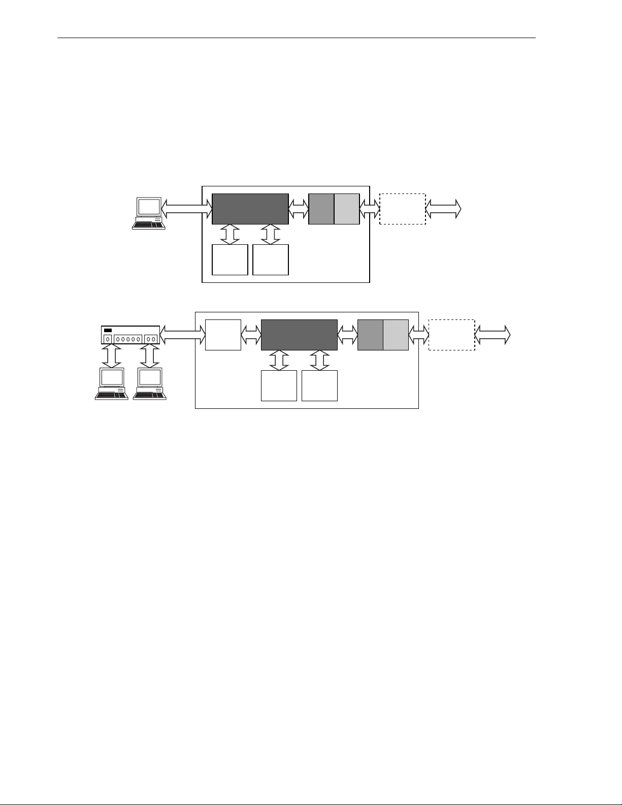
CHAPTER 1 INTRODUCTION
1.3 System Configuration
The µPD98502 can perform bridging and routing function between ADSL/ATM interface and USB/Ethernet
interface and provides this function in a single chip. By selecting user interface, examples of system configuration will
be realized as shown below. USB and Ethernet functions will exclusively operate each other.
HUB
Figure 1-1. Examples of the
USB/PCI
µ
PD98502
PC
SDRAM
100B-T
PCPC
Ethernet
PHY
µµµµ
PD98502 System Configuration
(a) ADSL MODEM
FLASH
(b) ADSL ROUTER
MII
µ
PD98502
SDRAM
ADSL
PHY
FLASH
ADSL
AFE
ADSL
PHY
POTS
SPLITTER
ADSL
AFE
ADSL
POTS
SPLITTER
ADSL
24
Preliminary User’s Manual S15543EJ1V0UM
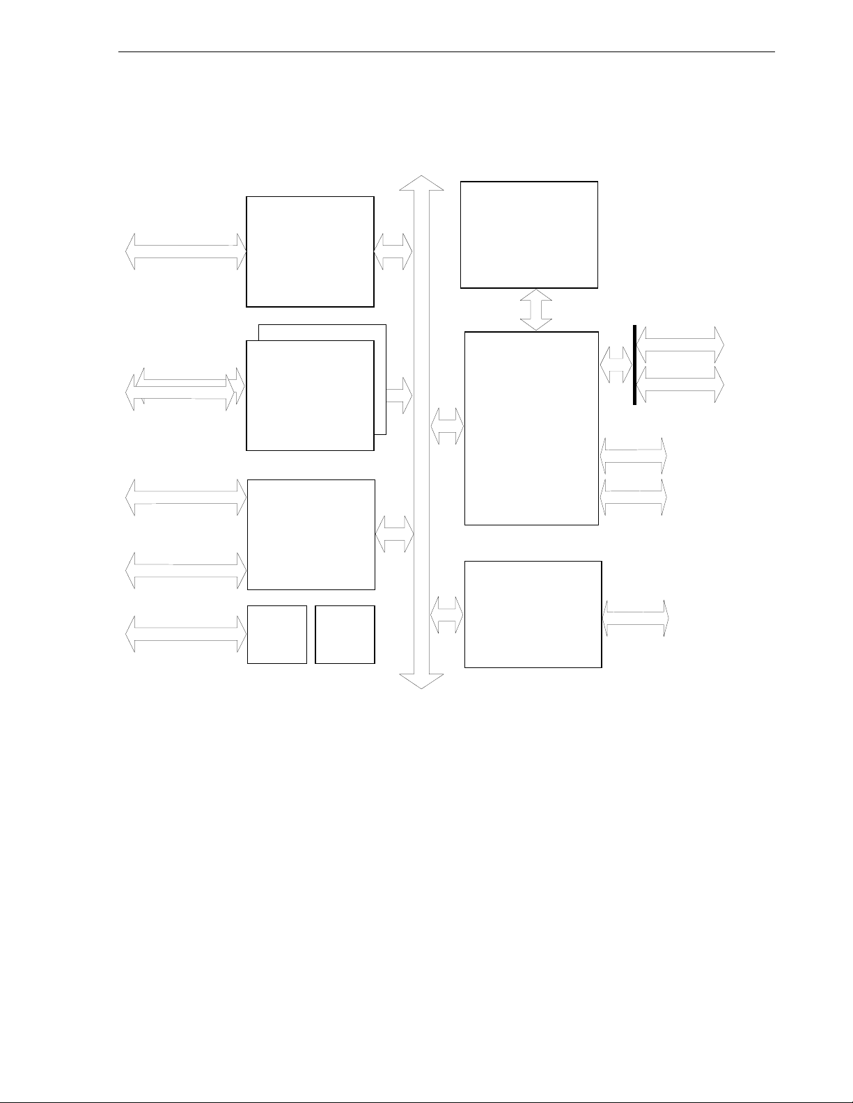
1.4 Block Diagram (Summary)
CHAPTER 1 INTRODUCTION
USB
3.3V MII
16.5/25/33 MHz
UTOPIA 2
PHY
Management
Figure 1-2. Block Diagram of the
Full-Speed USB
Controller
Ethernet
Controller
#1, #2
ATM Cell
Processor
IBUS
µµµµ
PD98502
VR4120A RISC
Processor Core
System
Controller
PROM/Flash
SDRAM
RS-232C/
Micro Wire
Parallel Port
JTAG
JTAG
Control
Clock
Control
PCI
Controller
32-bit
PCI Interface
Preliminary User’s Manual S15543EJ1V0UM
25
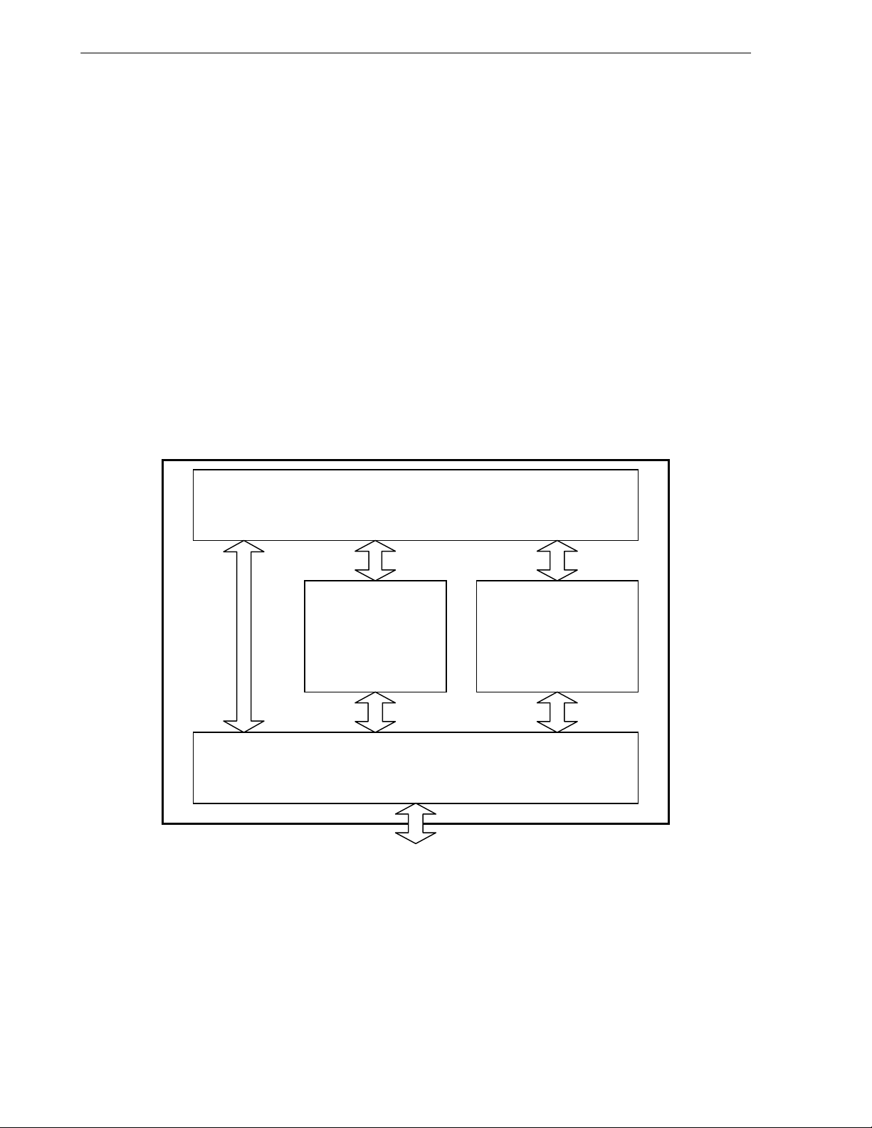
CHAPTER 1 INTRODUCTION
1.5 Block Diagram (Detail)
1.5.1 VR4120A RISC processor core
R
We will support real-time OS running on high performance RISC processor V
protocols (TCP/IP, PPP, SNMP, HTTP etc) to realize ADSL router and modem. Middleware including RTOS will be
loaded to SDRAM from external PROM and Flash ROM and by setting write protected area for such an area, high
speed processing will be realized together with large size instruction cache.
Features of VR
4120A RISC Processor Core are as follows;
• MIPS/I/II/III instruction set will be supported (FPU, LL, LLD, SC, SCD instruction will be excluded)
• Realize high speed processing of application by supporting high speed multiply and accumulate function
• Includes large size cache memory (Instruction: 16 Kbytes, Data: 8 Kbytes)
• Supports up to 1T byte virtual address space by using full associative TLB
• Implements switching function between Big-Endian and Little-Endian
4120A core and can perform network
Figure 1-3. Block Diagram of V
VR4120A RISC Processor Core
VR4120A Data Path
Data
Cache
(8 KBytes)
BUS Controller
R4120A RISC Processor
Instruction
Cache
(16 KBytes)
26
SysAD Bus
Preliminary User’s Manual S15543EJ1V0UM
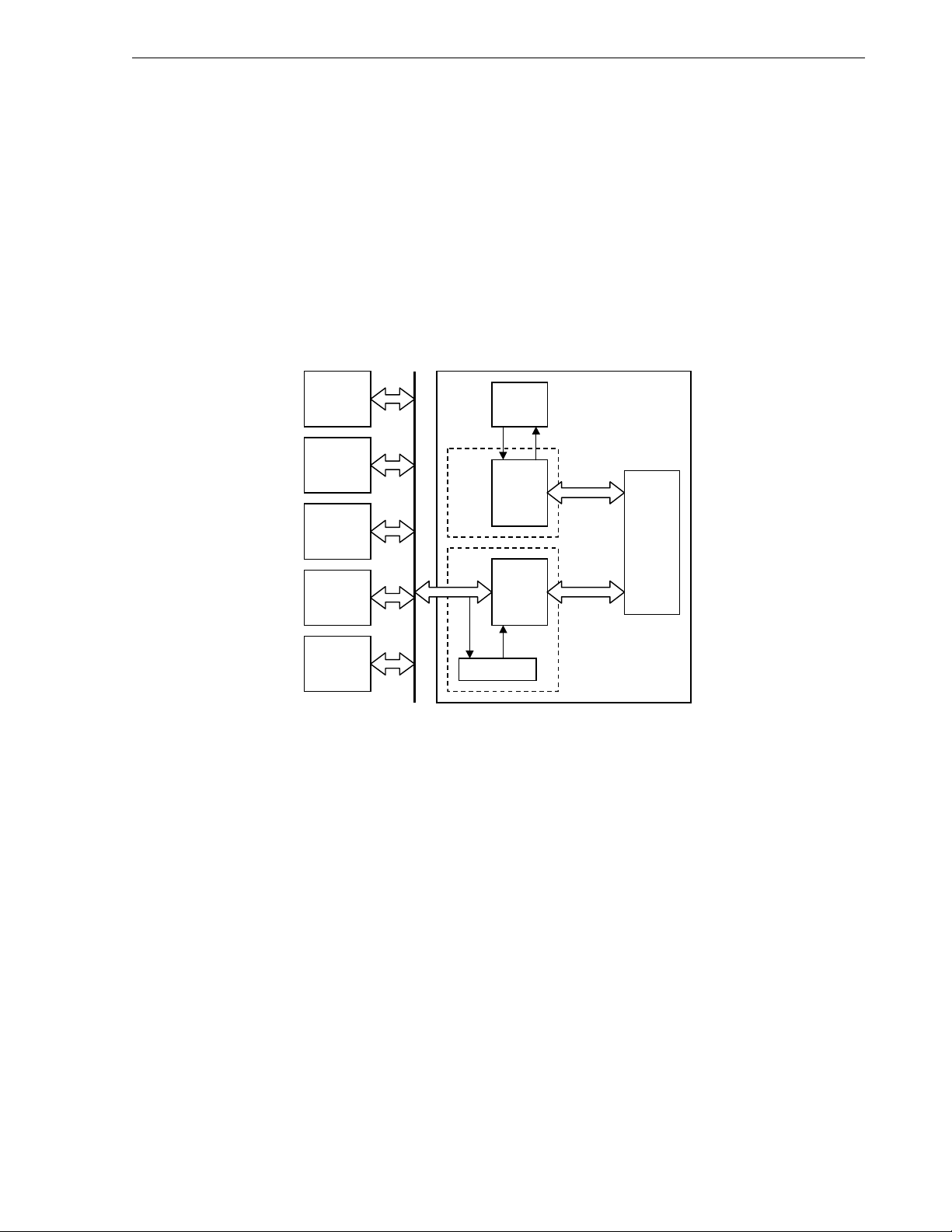
CHAPTER 1 INTRODUCTION
1.5.2 IBUS
The IBUS is a 32-bit, 66-MHz high-speed on-chip bus, which enables interconnection each controller blocks.
The IBUS supports the following bus protocols;
• Single read/write transfer
• Burst read/write transfer
• Slave lock
• Retry and disconnect
• Bus parking
Figure 1-4. Block Diagram of IBUS
System
Controller
ATM Cell
Processor
Ethernet
Controller
#1, #2
USB
Controller
PCI
Controller
IBUS
IBUS Interface Block
IBUS
arbiter
BUS MASTER
IBUS
Master
I/F
IBUS
MUX
IBUS
Slave
I/F
decoder
BUS SLAVE
(Using MUX Bus Arrangement)
Preliminary User’s Manual S15543EJ1V0UM
27
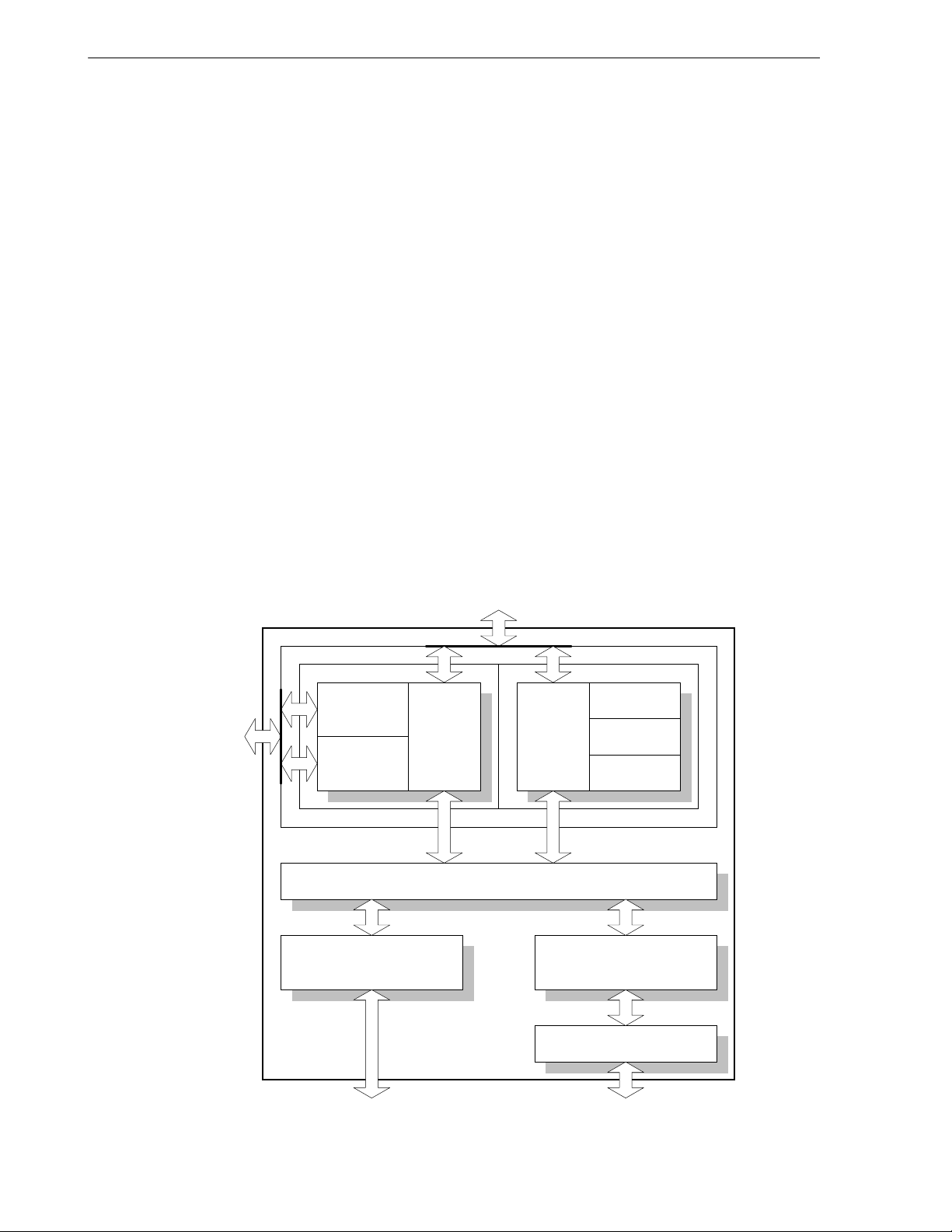
CHAPTER 1 INTRODUCTION
1.5.3 System controller
System Controller is
the VR
4120A System Bus “SysAD”, NEC original high-speed on-chip bus “IBUS” and memory bus for
PD98502’s internal system controller. System Controller provides bridging function among
µ
SDRAM/PROM/Flash.
Features of System Controller are as follows;
• Implements 4-word prefetch FIFO buffer between SysAD and Memory
• Implements 32-bit×64-word FIFO buffer for each Tx and Rx to IBUS
• Implements 32-bit× 4-word FIFO buffer for each Tx and Rx to HBUS
• Provides bus bridging function among SysAD bus and IBUS (internal bus) and Memory
• Supports Endian Converting function on SysAD bus
• Can directly connect SDRAM (MAX. 32 MBytes) and PROM/Flash (MAX. 8 MBytes) memory
4120A bus cycles at 66 MHz or 100 MHz
• Supports all V
R
• PROM/Flash data signals multiplexed on SDRAM data signals
• Supports 266-MB/sec (32 bits @66 MHz) bursts on IBUS
• Generates NMI and INT
• Supports NS16550 compatible Universal Asynchronous Receiver/Transmitter (UART)
• Supports separated 2-ch Timer
• Supports Deadman’s Switch Unit (Watch Dog Timer)
• Supports Micro Wire interface
Figure 1-5. Block Diagram of System Controller
System Controller
VRIF
MIF HIF
Flash
PROM
SDRAM
ROM-IF
SDRAM-IF
IBUS-HBUS Bridge
IHB
HBUS
HBUS
SysAD BUS
Memory
Arbitor
HBUS Arbiter
HARB
System
Bridge
REGISTER
HBUS
HBUS
PBUS-HBUS Bridge
PBUS
DSU
TIMER
PHB
28
IBUS
Preliminary User’s Manual S15543EJ1V0UM
RS-232C/Micro Wire
PFUR
FAST -UA RT
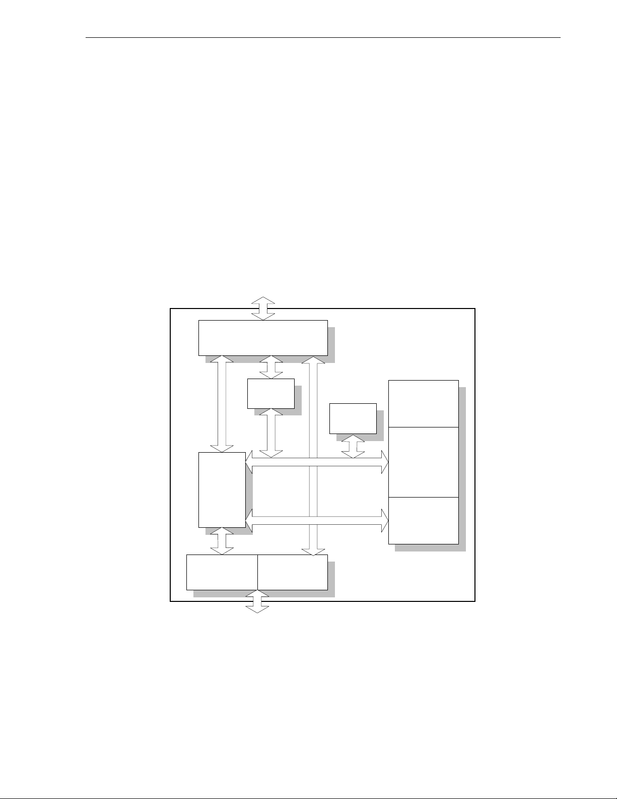
CHAPTER 1 INTRODUCTION
1.5.4 ATM cell processor
By using NEC proprietary 32-bit controller, we will realize ATM Cell processor Unit. ATM Cell processing by
firmware realizes more flexibility than before.
Features of ATM Cell Processor are as follows;
• Realize software SAR function by using 32-bit RISC controller (76 MIPS @66 MHz)
• Firmware is downloaded from external memory to Instruction Cache
• Supports 64 VCs
• Supports UTOPIA level 2 (including management interface) as PHY layer interface
• Supports processing AAL2, AAL5, Raw cell (AAL0) and F5 OAM cells
• Supports 3 service classes (CBR, VBR, UBR)
• Supports up to 50 Mbps Cell speed together with upstream and downstream
• Supports fine grain ATM cell shaping in 1cell/sec granularity on per VC basis
Figure 1-6. Block Diagram of ATM Cell Processor
IBUS Controller
UTOPIA
UTOPIA
BUS
BUS
Controller
Controller
UTOPIA2-I/F
UTOPIA2-I/F
(DATA)
(DATA)
IBUS
IBUS Controller
SAR
SAR
Registers
Registers
Read Only
UTOPIA2-I/F
UTOPIA2-I/F
(MANAGE)
(MANAGE)
ATM Cell Processor
DATA
DATA
WORK
WORK
RAM
RAM
RAM
RAM
RISC Core
RISC Core
I CACHE
I CACHE
IRAM
IRAM
UTOPIA2
Preliminary User’s Manual S15543EJ1V0UM
29
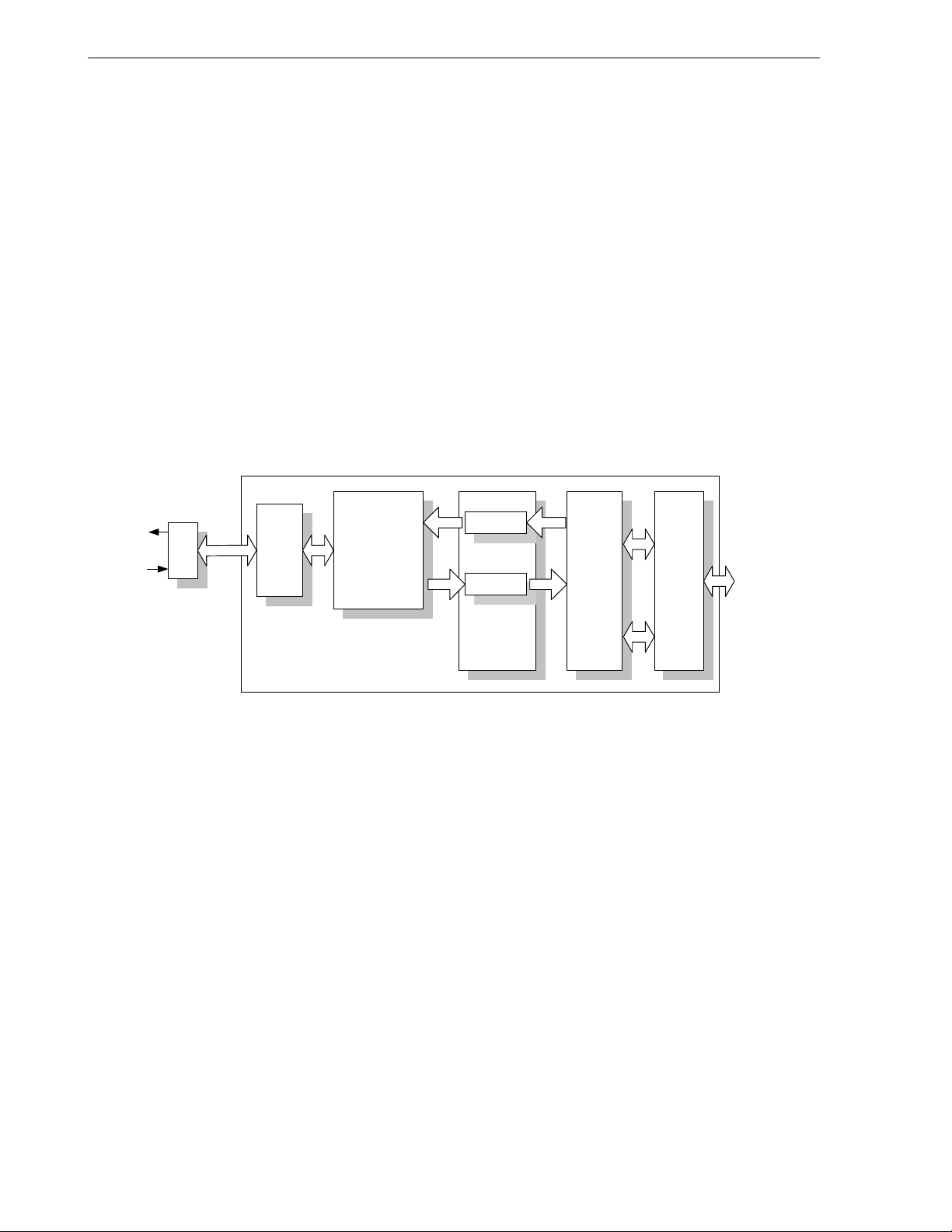
CHAPTER 1 INTRODUCTION
1.5.5 Ethernet controller
Ethernet Controller supports 2-channel 10 Mbps/100 Mbps Ethernet MAC (Media Access Control) function and MII
(Media Independent Interface) function.
Features of Ethernet Controller are as follows;
• Supports 10 M/100 M Ethernet MAC function compliant to IEEE802.3 and IEEE802.3u
• Supports 3.3 V MII compliant to IEEE802.3u
• Supports full duplex operation for both 100 Mbps and 10 Mbps
• Supports flow control function compliant to IEEE802.3x/D3.2
• Implements 256-Byte FIFO buffer for each Tx and Rx
• Implements address filtering functions for unicast/multicast/broadcast
• Implements MIB counters for network management (MIB II, Ether-like MIB, IEEE802.3LME are supported)
• Implements local DMA controller with individual DMA channels for each Tx and Rx
Figure 1-7. Block Diagram of Ethernet Controller
Ethernet Controller
TPO+
TPO-
TPI+
TPI-
Transceiver
MII
MII
I/O BU F
MAC
Core
Tx FIFO
Rx FIFO
FIFO
Cont.
DMAC
IBUS
IBUS
Controller
30
Preliminary User’s Manual S15543EJ1V0UM

CHAPTER 1 INTRODUCTION
1.5.6 USB controller
USB Controller provides Full Speed Function device function defined in Universal Serial Bus.
Features of USB Controller are as follows;
• Compliant to Universal Serial Bus Specification Rev. 1.1
4120A
• Supports Device class function by software running on V
R
• Performs 12 Mbps Full Speed USB function device (Hub function will be not supported)
• Can handle Suspend, Resume and Wake-up management signaling
• Supports Remote Wake-up.
• Implements 7 kinds of endpoints (Control, Interrupt IN/OUT, Isochronous IN/OUT, Bulk IN/OUT)
• Implements 64 Bytes FIFO buffer used for Control transfer for Tx
• Implements 128 Bytes FIFO buffer used for Isochronous transfer for Tx
• Implements 128 Bytes FIFO buffer used for Bulk transfer for Tx
• Implements 64 Bytes FIFO buffer used for Interrupt transfer for Tx
• Implements 128 Bytes shared FIFO buffer used for Control/Isochronous/Bulk/Interrupt transfer for Rx
• Implements local DMAC (DMA controller) block
• Can directly connect USB connector through USB dedicated I/O buffer
Figure 1-8. Block Diagram of USB Controller
USB
D+
D-
I/O
Buf
SIE EPC
USB CONTROLLER
MCONT
Tx FIFO
DMAC
Rx FIFO
BUS I/F
Master
I/F
Slave
I/F
slave
decoder
IBUS
Preliminary User’s Manual S15543EJ1V0UM
31

CHAPTER 1 INTRODUCTION
1.5.7 PCI controller
PCI Controller provides PCI Bus function defined by PCI SIG. This block is bridging between IBUS and PCI.
Features of PCI Controller are as follows;
• 32-bit PCI Interface (up to 33 MHz)
• 32-bit IBUS Interface (up to 33 MHz)
• Supports PCI Dual Address Cycle as master
• 33-MHz-PCI-frequency capable
• Compliant to PCI Local Bus Specification Rev. 2.2
• Compliant to PCI Bus Power Management Interface Rev. 1.1
• Supports up to 16 words burst for each directions
• Implements PCI bus arbiter that supports up to 4 external PCI-master devices at Host-mode
Figure 1-9. Block Diagram of PCI Bus controller
P2I
Control
PCI Slave
IBU S M aster
Data Flow
Control
PCI
Master
RegistersFIFO FIFO FIFO FIFO
IBU S S lave
PCI
Arbiter
I2P
Control
Idle
Control
32
Preliminary User’s Manual S15543EJ1V0UM

1.6 Pin Configuration (Bottom View)
• 500-pin Tape BGA (Heat spread type) (40 × 40)
PD98502N7-H6
µ
CHAPTER 1 INTRODUCTION
Index Mark
30
29
28
27
26
25
24
23
22
21
20
19
18
17
16
15
14
13
12
11
10
9
8
7
6
5
4
3
2
1
AK AJ AH AG
AF AE ADAC AB AA
YWV U T R PNM L K J HG F E DC B A
Preliminary User’s Manual S15543EJ1V0UM
33

CHAPTER 1 INTRODUCTION
Pin Name
Pin No. Pin Name Pin No. Pin Name Pin No. Pin Name Pin No. Pin Name Pin No. Pin Name
A1 SMA13 B10 URSDO C19 NJTRST D28 PGTO2_B F27 GND
A2 SMD0 B11 RMSL1 C20 IC-OPEN D29 PRQI1_B F28 GND
A3 SMD4 B12 MWDO C21 JDI D30 PAD0 F29 PAD5
A4 SMD7 B13 POM3 C22 GND E1 GND F30 PAD6
A5 SMD19 B14 POM5 C23 USBDM E2 SDRAS_B G1 SMA8
A6 SMD22 B15 EVDD C24 IC-OPEN E3 SMA0 G2 SMA15
A7 SRMCS_B B16 IC-OPEN C25 PUDGND E4 SMA10 G3 SDCLK1
A8 URDSR_B B17 IC-OPEN C26 IVDD E5 GND G4 EVDD
A9 URDCD_B B18 IC-OPEN C27 PMODE E6 EVDD G5 SDCAS_B
A10 URDTR_B B19 IC-OPEN C28 PGTO3_B E7 SMD16 G26 PAD1
A11 MWSK B20 GND C29 PGTO1_B E8 GND G27 PAD3
A12 MWDI B21 IC-PDn C30 PRQI0_B E9 EVDD G28 EVDD
A13 EXNMI B22 JDO D1 SDWE_B E10 GND G29 PAD7
A14 POM6 B23 GND D2 SMA1 E11 RMSL0 G30 PAD8
A15 EXINT B24 USBDP D3 SMA11 E12 GND H1 SMA4
A16 IVDD B25 PUDVD D4 IVDD E13 POM0 H2 SMA7
A17 IC-OPEN B26 IC-OPEN D5 SMD3 E14 GND H3 SMA9
A18 IC-PDnR B27 PUMD D6 SMD6 E15 POM7 H4 IVDD
A19 IC-OPEN B28 PHINT_B D7 EVDD E16 GND H5 GND
A20 IC-OPEN B29 PRSTO_B D8 IVDD E17 GND H26 GND
A21 IC-PDn B30 PGTO0_B D9 URCLK E18 IC-OPEN H27 IVDD
A22 JCK C1 SMA2 D10 IVDD E19 GND H28 PCBE0_B
A23 JMS C2 GND D11 GND E20 IC-PDn H29 PAD9
A24 EVDD C3 SMA16 D12 IVDD E21 GND H30 GND
A25 EVDD C4 SMD2 D13 POM1 E22 EVDD J1 SMA18
A26 PUAVD C5 GND D14 IVDD E23 GND J2 SMA3
A27 GND C6 SMD18 D15 IC-PDnR E24 USBCLK J3 SMA5
A28 IC-OPEN C7 SMD21 D16 BIG E25 EVDD J4 SMA6
A29 GND C8 SRMOE_B D17 IVDD E26 GND J5 EVDD
A30 PSERI_B C9 GND D18 IC-OPEN E27 PRQI3_B J26 EVDD
B1 SMA12 C10 URRTS_B D19 IVDD E28 PRQI2_B J27 PAD10
B2 SMA14 C11 EVDD D20 IC-OPEN E29 PAD2 J28 PAD11
B3 SMD1 C12 MWCS D21 IVDD E30 PAD4 J29 PAD12
B4 SMD5 C13 POM2 D22 JRSTB_B F1 SMA17 J30 PAD13
B5 SMD17 C14 POM4 D23 IVDD F2 SDCKE1 K1 SMD31
B6 SMD20 C15 ENDCEN D24 PUAGND F3 SDCS_B K2 SMA20
B7 SMD23 C16 GND D25 PUSTBY F4 GND K3 SMA19
B8 URCTS_B C17 NJTMS D26 PARBN F5 EVDD K4 IVDD
B9 URSDI C18 NJTDO D27 IVDD F26 EVDD K5 GND
(1/3)
34
Preliminary User’s Manual S15543EJ1V0UM

CHAPTER 1 INTRODUCTION
Pin No. Pin Name Pin No. Pin Name Pin No. Pin Name Pin No. Pin Name Pin No. Pin Name
K26 GND P5 GND V4 IVDD AB3 IC-PUp AF2 MICRS
K27 IVDD P26 GND V5 GND AB4 IC-PDn AF3 MIMCLK
K28 PAD14 P27 IVDD V26 PAD26 AB5 EVDD AF4 MITD3
K29 PAD15 P28 PAD16 V27 PAD25 AB26 EVDD AF5 GND
K30 EVDD P29 PAD17 V28 PAD24 AB27 IC-OPEN AF6 EVDD
L1 SDCLK0 P30 PAD18 V29 GND AB28 IC-OPEN AF7 MI2TE
L2 GND R1 EVDD V30 PSCLK AB29 GND AF8 GND
L3 SDCKE0 R2 SMD12 W1 IC-PUp AB30 RSTB AF9 EVDD
L4 SMD30 R3 SMD9 W2 IVDD AC1 IC-PUp AF10 GND
L5 EVDD R4 SMD10 W3 IC-PUp AC2 MIRD3 AF11 UDRD1
L26 PCBE1_B R5 SMD11 W4 IVDD AC3 GND AF12 GND
L27 GND R26 EVDD W5 GND AC4 IVDD AF13 UDRAD2
L28 PAR R27 PAD19 W26 GND AC5 GND AF14 GND
L29 PSERO_B R28 PAD20 W27 IVDD AC26 GND AF15 UDTAD3
L30 PER_B R29 GND W28 PAD28 AC27 IVDD AF16 UDTD7
M1 EVDD R30 PAD21 W29 EVDD AC28 IC-OPEN AF17 GND
M2 SMD28 T1 SMD8 W30 PAD27 AC29 IC-OPEN AF18 EVDD
M3 SMD29 T2 GND Y1 IC-OPEN AC30 PINT_B AF19 GND
M4 IVDD T3 CLKUSL1 Y2 PSDGND AD1 MIRD2 AF20 UMWR_B
M5 GND T4 CLKUSL0 Y3 PSAGND AD2 MIRD1 AF21 GND
M26 GND T5 EVDD Y4 PSAVD AD3 MIRCLK AF22 EVDD
M27 IVDD T26 PAD22 Y5 PSDVD AD4 MIRER AF23 GND
M28 PSTP_B T27 IVDD Y26 PAD31 AD5 MIRDV AF24 GND
M29 PDSEL_B T28 GND Y27 PME_B AD26 GND AF25 EVDD
M30 EVDD T29 PAD23 Y28 PRQO_B AD27 EVDD AF26 GND
N1 SMD24 T30 PCBE3_B Y29 PAD30 AD28 IC-PDnR AF27 GND
N2 SMD25 U1 CLKSL Y30 PAD29 AD29 IC-OPEN AF28 IC-PDnR
N3 GND U2 GND AA1 IC-OPEN AD30 GND AF29 IC-PDnR
N4 SMD26 U3 IC-PUp AA2 PSTBY AE1 MIRD0 AF30 IC-PDnR
N5 SMD27 U4 IVDD AA3 PSMD AE2 GND AG1 MIMD
N26 PTRY_B U5 GND AA4 IVDD AE3 MITER AG2 GND
N27 PIRY_B U26 GND AA5 GND AE4 IVDD AG3 MITD2
N28 GND U27 IVDD AA26 GND AE5 EVDD AG4 IVDD
N29 PFRA_B U28 PIDSEL AA27 IVDD AE26 EVDD AG5 MI2COL
N30 PCBE2_B U29 GND AA28 PGTI_B AE27 IC-PDnR AG6 IVDD
P1 SMD13 U30 EVDD AA29 GND AE28 IC-PDnR AG7 MI2CRS
P2 SMD14 V1 SCLK AA30 EVDD AE29 IC-PDnR AG8 IVDD
P3 SMD15 V2 GND AB1 IC-OPEN AE30 IC-PDnR AG9 UDRSC
P4 IVDD V3 IC-PUp AB2 GND AF1 MITE AG10 IVDD
(2/3)
Preliminary User’s Manual S15543EJ1V0UM
35

CHAPTER 1 INTRODUCTION
Pin No. Pin Name Pin No. Pin Name Pin No. Pin Name Pin No. Pin Name Pin No. Pin Name
AG11 UDRD0 AH3 MICOL AH25 EVDD AJ17 UDTD5 AK9 UDRD5
AG12 IVDD AH4 MI2RD0 AH26 IVDD AJ18 GND AK10 UDRD2
AG13 UDRAD1 AH5 MI2MD AH27 UMAD8 AJ19 UMRDY_B AK11 UDRCLK
AG14 IVDD AH6 MI2TER AH28 UMAD7 AJ20 GND AK12 UDRAD3
AG15 UDTAD2 AH7 MI2TD3 AH29 UMAD3 AJ21 EVDD AK13 UDRAD0
AG16 UDTAD0 AH8 GND AH30 UMAD1 AJ22 UMD13 AK14 UDTE_B
AG17 IVDD AH9 UDRCLV AJ1 MITD0 AJ23 UMD9 AK15 UDTAD4
AG18 UDTD1 AH10 UDRD4 AJ2 MI2MCLK AJ24 UMD7 AK16 UDTCLK
AG19 IVDD AH11 UDTCLV AJ3 MI2RD1 AJ25 UMD4 AK17 UDTD6
AG20 UMMD AH12 IC-OPEN AJ4 GND AJ26 UMD1 AK18 UDTD3
AG21 IVDD AH13 EVDD AJ5 MI2RER AJ27 GND AK19 UDTD0
AG22 UMD10 AH14 UDTSC AJ6 GND AJ28 GND AK20 UMRST_B
AG23 IVDD AH15 EVDD AJ7 MI2TD1 AJ29 UMAD6 AK21 UMRD_B
AG24 UMD2 AH16 UDTAD1 AJ8 UDRE_B AJ30 UMAD4 AK22 UMD14
AG25 UMAD11 AH17 UDTD4 AJ9 UDRD6 AK1 MI2RD3 AK23 UMD12
AG26 UMAD9 AH18 UDTD2 AJ10 UDRD3 AK2 MI2RD2 AK24 UMD8
AG27 IVDD AH19 UMINT_B AJ11 UDRAD4 AK3 MI2RCLK AK25 UMD6
AG28 UMAD2 AH20 UMSL_B AJ12 IC-OPEN AK4 MI2RDV AK26 UMD3
AG29 UMAD0 AH21 UMD15 AJ13 GND AK5 MI2TCLK AK27 UMD0
AG30 IVDD AH22 UMD11 AJ14 GND AK6 MI2TD2 AK28 UMAD10
AH1 MITCLK AH23 GND AJ15 IVDD AK7 MI2TD0 AK29 IC-PUp
AH2 MITD1 AH24 UMD5 AJ16 GND AK8 UDRD7 AK30 UMAD5
(3/3)
Special pin name description:
IC-PDn: Pull Down
IC-PDnR: Pull Down with Resistor
IC-PUp: Pull Up
IC-PUpR: Pull Up with Resistor
Remark In this document, XXX_B stands for active low pin.
36
Preliminary User’s Manual S15543EJ1V0UM

CHAPTER 1 INTRODUCTION
1.7 Pin Function
Symbol of I/O column indicates following status in this section.
I : Input
O : Output
I/O : Bidirection
I/OZ : Bidirection (Include Hi-Z state)
I/OD : Bidirection (Open drain output)
OZ : Output (Include Hi-Z state)
OD : Output (Open drain)
1.7.1 Power supply
Pin Name Pin No. I/O Active Level Function
GND A27, A29, B20, B23, C16, C2, C22, C5, C9, D11, E1, E10,
E12, E14, E16, E17, E19, E21, E23, E26, E5, E8, F27,
F28, F4, H26, H30, H5, K26, K5, L2, L27, M26, M5, N28,
N3, P26, P5, R29, T2, T28, U2, U26, U29, U5, V2, V29, V5,
W26, W5, AA26, AA29, AA5, AB2, AB29, AC26, AC3, AC5,
AD26, AD30, AE2, AF10, AF12, AF14, AF17, AF19, AF21,
AF23, AF24, AF26, AF27, AF5, AF8, AG2, AH23, AH8,
AJ13, AJ14, AJ16, AJ18, AJ20, AJ27, AJ28, AJ4, AJ6
IVDD A16, C26, D10, D12, D14, D17, D19, D21, D23, D27, D4,
D8, H27, H4, K27, K4, M27, M4, P27, P4, T27, U27, U4,
V4, W2, W27, W4, AA27, AA4, AC27, AC4, AE4, AG10,
AG12, AG14, AG17, AG19, AG21, AG23, AG27, AG30,
AG4, AG6, AG8, AH26, AJ15
EVDD A24, A25, B15, C11, D7, E22, E25, E6, E9, F26, F5, G28,
G4, J26, J5, K30, L5, M1, M30, R1, R26, T5, U30, W29,
AA30, AB26, AB5, AD27, AE26, AE5, AF18, AF22, AF25,
AF6, AF9, AH13, AH15, AH25, AJ21
GND (0 V)
Internal logic core
power supply (+2.5 V)
External (I/O) power
supply (+3.3 V)
1.7.2 System PLL power supply
Pin Name Pin No. I/O Active Level Function
PSAGND Y3 I Analog ground
PSAVD Y4 I Analog power supply
PSDGND Y2 I Digital ground
PSDVD Y5 I Digital power supply
1.7.3 USB PLL power supply
Pin Name Pin No. I/O Active Level Function
PUAGND D24 I Analog ground
PUAVD A26 I Analog power supply
PUDGND C25 I Digital ground
PUDVD B25 I Digital power supply
Preliminary User’s Manual S15543EJ1V0UM
37

CHAPTER 1 INTRODUCTION
1.7.4 System control interface
Pin Name Pin No. I/O Active Level Function
SCLK V1 I System clock (33 MHz)
CLKSL U1 I Clock select (100 MHz/66 MHz)
PSMD AA3 I System PLL mode control (0: normal, 1: through)
PSTBY AA2 I System PLL standby mode control (0: active, 1: standby)
PUMD B27 I USB PLL mode control (0: normal, 1: through)
PUSTBY D25 I USB PLL standby mode control (0: active, 1: standby)
BIG D16 I H VR4120 big endian mode
ENDCEN C15 I Endian conversion enable
EXINT_B A15 I L External interrupt
EXNM_BI A13 I L External non-maskable interrupt
RSTB_B AB30 I L System reset
RMSL0 E11 I ROM access bus width select
RMSL1 B11 I (RMSL1/0 = L/L: 32-bit, L/H: 16-bit, H/L: 8-bit)
38
Preliminary User’s Manual S15543EJ1V0UM

CHAPTER 1 INTRODUCTION
1.7.5 Memory interface
Pin Name Pin No. I/O Active Level Function
SDCLK0 L1 O SDRAM clock
SDCLK1 G3 O SDRAM clock
SDCKE0 L3 O H SDRAM clock enable
SDCKE1 F2 O H SDRAM clock enable
SDCS_B F3 O L Chip select
SDRAS_B E2 O L Row address strobe
SDCAS_B G5 O L Column address strobe
SDWE_B D1 O L Write enable
SRMCS_B A7 O L PROM/FLASH chip select
SRMOE_B C8 O L PROM/FLASH output enable
SMA0 E3 O Memory address
SMA1 D2 O Memory address
SMA2 C1 O Memory address
SMA3 J2 O Memory address
SMA4 H1 O Memory address
SMA5 J3 O Memory address
SMA6 J4 O Memory address
SMA7 H2 O Memory address
SMA8 G1 O Memory address
SMA9 H3 O Memory address
SMA10 E4 O Memory address
SMA11 D3 O Memory address
SMA12 B1 O Memory address
SMA13 A1 O Memory address
SMA14 B2 O Memory address
SMA15 G2 O Memory address
SMA16 C3 O Memory address
SMA17 F1 O Memory address
SMA18 J1 O Memory address
SMA19 K3 O Memory address
SMA20 K2 O Memory address
SMD0 A2 I/O Memory data
SMD1 B3 I/O Memory data
SMD2 C4 I/O Memory data
SMD3 D5 I/O Memory data
SMD4 A3 I/O Memory data
SMD5 B4 I/O Memory data
SMD6 D6 I/O Memory data
SMD7 A4 I/O Memory data
SMD8 T1 I/O Memory data
SMD9 R3 I/O Memory data
SMD10 R4 I/O Memory data
(1/2)
Preliminary User’s Manual S15543EJ1V0UM
39

CHAPTER 1 INTRODUCTION
Pin Name Pin No. I/O Active Level Function
SMD11 R5 I/O Memory data
SMD12 R2 I/O Memory data
SMD13 P1 I/O Memory data
SMD14 P2 I/O Memory data
SMD15 P3 I/O Memory data
SMD16 E7 I/O Memory data
SMD17 B5 I/O Memory data
SMD18 C6 I/O Memory data
SMD19 A5 I/O Memory data
SMD20 B6 I/O Memory data
SMD21 C7 I/O Memory data
SMD22 A6 I/O Memory data
SMD23 B7 I/O Memory data
SMD24 N1 I/O Memory data
SMD25 N2 I/O Memory data
SMD26 N4 I/O Memory data
SMD27 N5 I/O Memory data
SMD28 M2 I/O Memory data
SMD29 M3 I/O Memory data
SMD30 L4 I/O Memory data
SMD31 K1 I/O Memory data
(2/2)
40
Preliminary User’s Manual S15543EJ1V0UM

CHAPTER 1 INTRODUCTION
1.7.6 PCI interface
Pin Name Pin No. I/O Active Level Function
PSCLK V30 I PCI clock
PARBN D26 I PCI arbiter enable
PMODE C27 I PCI mode select (L: host, H: NIC)
PIDSEL U28 I H Initialization device select
PDSEL_B M29 I/OZ L Device select
PER_B L30 I/OZ L Parity error
PFRA_B N29 I/OZ L Cycle frame
PHINT_B B28 I L PCI host interrupt
PINT_B AC30 O L Interrupt_A
PIRY_B N27 I/OZ L Initiator ready
PME_B Y27 OD L Power management event
PRSTO_B B29 O L PCI system reset out
PSERI_B A30 I L System error in
PSERO_B L29 O L System error out
PTRY_B N26 I/OZ L Target ready
PSTP_B M28 I/OZ L Stop request from target
PCBE0_B H28 I/OZ L Bus command and byte enable
PCBE1_B L26 I/OZ L Bus command and byte enable
PCBE2_B N30 I/OZ L Bus command and byte enable
PCBE3_B T30 I/OZ L Bus command and byte enable
PRQO_B Y28 O L Bus request out
PRQI0_B C30 I L Bus request in[0]
PRQI1_B D29 I L Bus request in[1]
PRQI2_B E28 I L Bus request in[2]
PRQI3_B E27 I L Bus request in[3]
PGTI_B AA28 I L Bus grant in
PGTO0_B B30 O L Bus grant out[0]
PGTO1_B C29 O L Bus grant out[1]
PGTO2_B D28 O L Bus grant out[2]
PGTO3_B C28 O L Bus grant out[3]
PAR L28 I/OZ Parity of address/data
PAD0 D30 I/OZ PCI address and data
PAD1 G26 I/OZ PCI address and data
PAD2 E29 I/OZ PCI address and data
PAD3 G27 I/OZ PCI address and data
PAD4 E30 I/OZ PCI address and data
PAD5 F29 I/OZ PCI address and data
PAD6 F30 I/OZ PCI address and data
PAD7 G29 I/OZ PCI address and data
PAD8 G30 I/OZ PCI address and data
PAD9 H29 I/OZ PCI address and data
PAD10 J27 I/OZ PCI address and data
(1/2)
Preliminary User’s Manual S15543EJ1V0UM
41

CHAPTER 1 INTRODUCTION
Pin Name Pin No. I/O Active Level Function
PAD11 J28 I/OZ PCI address and data
PAD12 J29 I/OZ PCI address and data
PAD13 J30 I/OZ PCI address and data
PAD14 K28 I/OZ PCI address and data
PAD15 K29 I/OZ PCI address and data
PAD16 P28 I/OZ PCI address and data
PAD17 P29 I/OZ PCI address and data
PAD18 P30 I/OZ PCI address and data
PAD19 R27 I/OZ PCI address and data
PAD20 R28 I/OZ PCI address and data
PAD21 R30 I/OZ PCI address and data
PAD22 T26 I/OZ PCI address and data
PAD23 T29 I/OZ PCI address and data
PAD24 V28 I/OZ PCI address and data
PAD25 V27 I/OZ PCI address and data
PAD26 V26 I/OZ PCI address and data
PAD27 W30 I/OZ PCI address and data
PAD28 W28 I/OZ PCI address and data
PAD29 Y30 I/OZ PCI address and data
PAD30 Y29 I/OZ PCI address and data
PAD31 Y26 I/OZ PCI address and data
(2/2)
42
Preliminary User’s Manual S15543EJ1V0UM

CHAPTER 1 INTRODUCTION
1.7.7 ATM interface
1.7.7.1 UTOPIA management interface
Pin Name Pin No. I/O Active Level Function
UMMD AG20 O Management mode select
UMINT_B AH19 I L Interrupt from PHY
UMRD_B AK21 O L Management read enable
UMRDY_B AJ19 I L Management data ready
UMRST_B AK20 O L PHY reset
UMSL_B AH20 O L PHY select
UMWR_B AF20 O L Management write enable
UMAD0 AG29 O PHY address
UMAD1 AH30 O PHY address
UMAD2 AG28 O PHY address
UMAD3 AH29 O PHY address
UMAD4 AJ30 O PHY address
UMAD5 AK30 O PHY address
UMAD6 AJ29 O PHY address
UMAD7 AH28 O PHY address
UMAD8 AH27 O PHY address
UMAD9 AG26 O PHY address
UMAD10 AK28 O PHY address
UMAD11 AG25 O PHY address
UMD0 AK27 I/O Management data
UMD1 AJ26 I/O Management data
UMD2 AG24 I/O Management data
UMD3 AK26 I/O Management data
UMD4 AJ25 I/O Management data
UMD5 AH24 I/O Management data
UMD6 AK25 I/O Management data
UMD7 AJ24 I/O Management data
UMD8 AK24 I/O Management data
UMD9 AJ23 I/O Management data
UMD10 AG22 I/O Management data
UMD11 AH22 I/O Management data
UMD12 AK23 I/O Management data
UMD13 AJ22 I/O Management data
UMD14 AK22 I/O Management data
UMD15 AH21 I/O Management data
Preliminary User’s Manual S15543EJ1V0UM
43

CHAPTER 1 INTRODUCTION
1.7.7.2 UTOPIA data interface
Pin Name Pin No. I/O Active Level Function
CLKUSL0 T4 I UTOPIA clock select
CLKUSL1 T3 I (CLKUSL1/0 = L/L: 33 MHz, H/L: 25 MHz, L/H: 16.5 MHz)
UDRCLK AK11 O Receive clock
UDRCLV AH9 I H Receive cell available
UDRE_B AJ8 O L Receive enable
UDRSC AG9 I H Receive cell start
UDRAD0 AK13 O Receive PHY address
UDRAD1 AG13 O Receive PHY address
UDRAD2 AF13 O Receive PHY address
UDRAD3 AK12 O Receive PHY address
UDRAD4 AJ11 O Receive PHY address
UDRD0 AG11 I Receive data
UDRD1 AF11 I Receive data
UDRD2 AK10 I Receive data
UDRD3 AJ10 I Receive data
UDRD4 AH10 I Receive data
UDRD5 AK9 I Receive data
UDRD6 AJ9 I Receive data
UDRD7 AK8 I Receive data
UDTCLK AK16 O Transmit clock
UDTCLV AH11 I H Transmit cell available
UDTE_B AK14 O L Transmit enable
UDTSC AH14 O H Transmit cell start position
UDTAD0 AG16 O Transmit PHY address
UDTAD1 AH16 O Transmit PHY address
UDTAD2 AG15 O Transmit PHY address
UDTAD3 AF15 O Transmit PHY address
UDTAD4 AK15 O Transmit PHY address
UDTD0 AK19 O Transmit data
UDTD1 AG18 O Transmit data
UDTD2 AH18 O Transmit data
UDTD3 AK18 O Transmit data
UDTD4 AH17 O Transmit data
UDTD5 AJ17 O Transmit data
UDTD6 AK17 O Transmit data
UDTD7 AF16 O Transmit data
44
Preliminary User’s Manual S15543EJ1V0UM

CHAPTER 1 INTRODUCTION
1.7.8 Ethernet interface
1.7.8.1 Ethernet interface (Channel 1)
Pin Name Pin No. I/O Active Level Function
MIMCLK AF3 O MII management clock
MIMD AG1 I/O MII management
MICOL AH3 I Collision
MICRS AF2 I Carrier sense
MIRCLK AD3 I Receive clock (2.5/25 MHz)
MIRDV AD5 I Receive data valid
MIRER AD4 I Receive error
MIRD0 AE1 I Receive data
MIRD1 AD2 I Receive data
MIRD2 AD1 I Receive data
MIRD3 AC2 I Receive data
MITCLK AH1 I Transmit clock (2.5/25 MHz)
MITE AF1 O Transmit enable
MITER AE3 O Transmit error
MITD0 AJ1 O Transmit data
MITD1 AH2 O Transmit data
MITD2 AG3 O Transmit data
MITD3 AF4 O Transmit data
Preliminary User’s Manual S15543EJ1V0UM
45

CHAPTER 1 INTRODUCTION
1.7.8.2 Ethernet interface (Channel 2)
Pin Name Pin No. I/O Active Level Function
MI2MCLK AJ2 O MII management clock
MI2MD AH5 I/O MII management
MI2COL AG5 I Collision
MI2CRS AG7 I Carrier sense
MI2RCLK AK3 I Receive clock (2.5/25 MHz)
MI2RDV AK4 I Receive data valid
MI2RER AJ5 I Receive error
MI2RD0 AH4 I Receive data
MI2RD1 AJ3 I Receive data
MI2RD2 AK2 I Receive data
MI2RD3 AK1 I Receive data
MI2TCLK AK5 I Transmit clock (2.5/25 MHz)
MI2TE AF7 O Transmit enable
MI2TER AH6 O Transmit error
MI2TD0 AK7 O Transmit data
MI2TD1 AJ7 O Transmit data
MI2TD2 AK6 O Transmit data
MI2TD3 AH7 O Transmit data
1.7.9 USB interface
Pin Name Pin No. I/O Active Level Function
USBCLK E24 I External USB clock
USBDM C23 I/O USB data(–)
USBDP B24 I/O USB data(+)
46
Preliminary User’s Manual S15543EJ1V0UM

CHAPTER 1 INTRODUCTION
1.7.10 UART interface
Pin Name Pin No. I/O Active Level Function
URCLK D9 I UART external clock
URCTS_B B8 I L UART clear to send
URDCD_B A9 I L UART data carrier detect
URDSR_B A8 I L UART data set ready
URDTR_B A10 O L UART data terminal ready
URRTS_B C10 O L UART data request to send
URSDI B9 I UART serial data input
URSDO B10 O UART serial data output
1.7.11 Micro Wire interface
Pin Name Pin No. I/O Active Level Function
MWCS C12 O Micro Wire chip select
MWDI A12 I Micro Wire data in
MWDO B12 O Micro Wire data out
MWSK A11 O Micro Wire SK
1.7.12 Parallel port interface
Pin Name Pin No. I/O Active Level Function
POM0 E13 O Parallel port signal output
POM1 D13 O Parallel port signal output
POM2 C13 O Parallel port signal output
POM3 B13 O Parallel port signal output
POM4 C14 O Parallel port signal output
POM5 B14 O Parallel port signal output
POM6 A14 O Parallel port signal output
POM7 E15 O Parallel port signal output
1.7.13 Boundary scan interface
Pin Name Pin No. I/O Active Level Function
JCK A22 I B-SCAN clock
JDI C21 I B-SCAN input-data
JDO B22 t/s O B-SCAN output-data
JMS A23 I B-SCAN mode select
JRSTB_B D22 I L B-SCAN reset
Preliminary User’s Manual S15543EJ1V0UM
47

CHAPTER 1 INTRODUCTION
1.7.14 I.C. – open
Pin Name Pin No. I/O Active Level Function
IC-OPEN A17, A19, A20, A28, B16, B17, B18, B19, B26, C20, C24,
D18, D20, E18, Y1, AA1, AB1, AB27, AB28, AC28, AC29,
AD29, AH12, AJ12
O
1.7.15 I.C.– pull down
Pin Name Pin No. I/O Active Level Function
IC-PDn A21, B21, E20, AB4 I
1.7.16 I.C. – pull down with resistor
Pin Name Pin No. I/O Active Level Function
IC-PDnR
A18, D15, AE30, AD28, AE27, AE28, AE29, AF28, AF29,
AF30
I/O
1.7.17 I.C. – pull up
Pin Name Pin No. I/O Active Level Function
IC-PUp U3, V3, W1, W3, AB3, AC1, AK29 I
48
Preliminary User’s Manual S15543EJ1V0UM

1.8 I/O Register Map
CHAPTER 1 INTRODUCTION
Core Offset Register
Length
Name Access by
V
4120A
R
Description
(Byte)
ATM F000H 4 A_GMR R/W General Mode Register
ATM F004H 4 A_GSR R General Status Register
ATM F008H 4 A_IMR R/W Interrupt Mask Register
ATM F00CH 4 A_RQU R Receive Queue Underrunning
ATM F010H 4 A_RQA R Receive Queue Alert
ATM F014H - N/A - Reserved for future use
ATM F018H 4 A_VER R Version Number
ATM F01CH - N/A - Reserved for future use
ATM F020H 4 A_CMR R/W Command Register
ATM F024H - N/A - Reserved for future use
ATM F028H 4 A_CER R/W Command Extension Register
ATM F02CH-F04CH - N/A - Reserved for future use
ATM F050H 4 A_MSA0 R/W Mailbox0 Start Address
ATM F054H 4 A_MSA1 R/W Mailbox1 Start Address
ATM F058H 4 A_MSA2 R/W Mailbox2 Start Address
ATM F05CH 4 A_MSA3 R/W Mailbox3 Start Address
ATM F060H 4 A_MBA0 R/W Mailbox0 Bottom Address
ATM F064H 4 A_MBA1 R/W Mailbox1 Bottom Address
ATM F068H 4 A_MBA2 R/W Mailbox2 Bottom Address
ATM F06CH 4 A_MBA3 R/W Mailbox3 Bottom Address
ATM F070H 4 A_MTA0 R/W Mailbox0 Tail Address
ATM F074H 4 A_MTA1 R/W Mailbox1 Tail Address
ATM F078H 4 A_MTA2 R/W Mailbox2 Tail Address
ATM F07CH 4 A_MTA3 R/W Mailbox3 Tail Address
ATM F080H 4 A_MWA0 R/W Mailbox0 Write Address
ATM F084H 4 A_MWA1 R/W Mailbox1 Write Address
ATM F088H 4 A_MWA2 R/W Mailbox2 Write Address
ATM F08CH 4 A_MWA3 R/W Mailbox3 Write Address
ATM F090H 4 A_RCC R Valid Receiving Cell Counter
ATM F094H 4 A_TCC R Valid Transmitting Cell Counter
ATM F098H 4 A_RUEC R Receive Unprovisioned VPI/VCI Error Cell Counter
ATM F09CH 4 A_RIDC R Receiving Internal Discarded Cell Counter
ATM F0A0H-F0AFH - N/A - Reserved for future use
ATM F0B0H-F0B3H - N/A - Reserved for future use
ATM F0B4H-F0BCH - N/A - Reserved for future use
ATM F0C0H 4 A_T1R R/W T1 Timer Register
ATM F0C4H - N/A - Reserved for future use
ATM F0C8H 4 A_TSR R/W Time Stamp Register
ATM F200H-F2FFH - N/A - Can not access from VR4120A RISC Core.
ATM F300H 4 A_IBBAR R/W IBUS Base Address Register
ATM F304H 4 A_INBAR R/W Instruction Base Address Register
ATM F308H- F31FH - N/A - Reserved for future use
ATM F320H 4 A_UMCMD R/W UTOPIA Management Interface Command Register
ATM F324H- F3FFH - N/A - Reserved for future use
ATM F400H-F4FFH - N/A - Can not access from VR4120A RISC Core.
ATM F500H-FFFFH - N/A - Reserved for future use
PCI 000H 4 P_PLBA R/W PCI Lower Base Address
PCI 008H 4 P_IBBA R/W Internal bus Base Address
PCI 000H 4 P_PLBA R/W PCI Lower Base Address
PCI 008H 4 P_IBBA R/W Internal bus Base Address
PCI 00CH 4 N/A - Reserved for future use
PCI 010H 4 P_VERR R Version Register
PCI 014H 4 P_PCAR R/W PCI Configuration Address Register
PCI 018H 4 P_PCDR R/W PCI Configuration Data Register
PCI 01CH 4 P_IGSR R Internal bus General Status Register
PCI 020H 4 P_IIMR R/W Internal bus Interrupt Mask Register
PCI 024H 4 P_PGSR R/W PCI General Status Register
PCI 028H 4 P_PIMR R/W PCI Interrupt Mask Register
PCI 02CH 4 N/A - Reserved for future use
PCI 030H 4 P_HMCR R/W Host Mode Control Register
PCI 034H-03CH 4 N/A - Reserved for future use
PCI 040H 4 P_PWCD R/W Power Consumption Data Register
PCI 044H 4 P_PWDD R/W Power Dissipation Data Register
Preliminary User’s Manual S15543EJ1V0UM
49

CHAPTER 1 INTRODUCTION
Core Offset Register
Length
Name Access by
V
4120A
R
Description
(Byte)
PCI 048H-04CH 4 N/A - Reserved for future use
PCI 050H 4 P_BCNT R/W Bridge Control Register
PCI 054H 4 P_PPCR R/W Power Control Register
PCI 058H 4 P_SWRR W Software Reset Register
PCI 05CH 4 P_PTMR R/W Retry Timer Register
PCI 060H-0FFH 4 N/A - Reserved for future use
PCI 100H-1FFH 4 P_CONFIG (*) Configuration Registers.
* Some registers are R/W. Other registers are Read only.
Ether 00H 4 En_MACC1 R/W MAC configuration register 1
Ether 04H 4 En_MACC2 R/W MAC configuration register 2
Ether 08H 4 En_IPGT R/W Back-to-Back IPG register
Ether 0CH 4 En_IPGR R/W Non Back-to-Back IPG register
Ether 10H 4 En_CLRT R/W Collision register
Ether 14H 4 En_LMAX R/W Max packet length register
Ether 18H-1CH - N/A - Reserved for future use
Ether 20H 4 En_RETX R/W Retry count register
Ether 24H-50H - N/A - Reserved for future use
Ether 54H 4 En_LSA2 R/W Station Address register 2
Ether 58H 4 En_LSA1 R/W Station Address register 1
Ether 5CH 4 En_PTVR R Pause timer value read register
Ether 60H - N/A - Reserved for future use
Ether 64H 4 En_VLTP R/W VLAN type register
Ether 80H 4 En_MIIC R/W MII configuration register
Ether 84H-90H - N/A - Reserved for future use
Ether 94H 4 En_MCMD W MII command register
Ether 98H 4 En_MADR R/W MII address register
Ether 9CH 4 En_MWTD R/W MII write data register
Ether A0H 4 En_MRDD R MII read data register
Ether A4H 4 En_MIND R MII indicator register
Ether A8H-C4H - N/A - Reserved for future use
Ether CCH 4 En_HT1 R/W Hash table register 1
Ether D0H 4 En_HT2 R/W Hash table register 2
Ether D4H-D8H - N/A - Reserved for future use
Ether DCH 4 En_CAR1 R/W Carry register 1
Ether E0H 4 En_CAR2 R/W Carry register 2
Ether E4H-12CH - N/A - Reserved for future use
Ether 130H 4 En_CAM1 R/W Carry mask register 1
Ether 134H 4 En_CAM2 R/W Carry mask register 2
Ether 138H-13CH - N/A - Reserved for future use
Ether 140H 4 En_RBYT R/W Receive Byte Counter
Ether 144H 4 En_RPKT R/W Receive Packet Counter
Ether 148H 4 En_RFCS R/W Receive FCS Error Counter
Ether 14CH 4 En_RMCA R/W Receive Multicast Packet Counter
Ether 150H 4 En_RBCA R/W Receive Broadcast Packet Counter
Ether 154H 4 En_RXCF R/W Receive Control Frame Packet Counter
Ether 158H 4 En_RXPF R/W Receive PAUSE Frame Packet Counter
Ether 15CH 4 En_RXUO R/W Receive Unknown OP code Counter
Ether 160H 4 En_RALN R/W Receive Alignment Error Counter
Ether 164H 4 En_RFLR R/W Receive Frame Length Out of Range Counter
Ether 168H 4 En_RCDE R/W Receive Code Error Counter
Ether 16CH 4 En_RFCR R/W Receive False Carrier Counter
Ether 170H 4 En_RUND R/W Receive Undersize Packet Counter
Ether 174H 4 En_ROVR R/W Receive Oversize Packet Counter
Ether 178H 4 En_RFRG R/W Receive Error Undersize Packet Counter
Ether 17CH 4 En_RJBR R/W Receive Error Oversize Packet Counter
Ether 180H 4 En_R64 R/W Receive 64 Byte Frame Counter
Ether 184H 4 En_R127 R/W Receive 65 to 127 Byte Frame Counter
Ether 188H 4 En_R255 R/W Receive 128 to 255 Byte Frame Counter
Ether 18CH 4 En_R511 R/W Receive 256 to 511 Byte Frame Counter
Ether 190H 4 En_R1K R/W Receive 512 to 1023 Byte Frame Counter
Ether 194H 4 En_RMAX R/W Receive Over 1023 Byte Frame Counter
Ether 198H 4 En_RVBT R/W Receive Valid Byte Counter
Ether 1C0H 4 En_TBYT R/W Transmit Byte Counter
Ether 1C4H 4 En_TPCT R/W Transmit Packet Counter
Ether 1C8H 4 En_TFCS R/W Transmit CRC Error Packet Counter
Ether 1CCH 4 En_TMCA R/W Transmit Multicast Packet Counter
50
Preliminary User’s Manual S15543EJ1V0UM

CHAPTER 1 INTRODUCTION
Core Offset Register
Length
Name Access by
V
4120A
R
Description
(Byte)
Ether 1D0H 4 En_TBCA R/W Transmit Broadcast Packet Counter
Ether 1D4H 4 En_TUCA R/W Transmit Unicast Packet Counter
Ether 1D8H 4 En_TXPF R/W Transmit PAUSE control Frame Counter
Ether 1DCH 4 En_TDFR R/W Transmit Single Deferral Packet Counter
Ether 1E0H 4 En_TXDF R/W Transmit Excessive Deferral Packet Counter
Ether 1E4H 4 En_TSCL R/W Transmit Single Collision Packet Counter
Ether 1E8H 4 En_TMCL R/W Transmit Multiple collision Packet Counter
Ether 1ECH 4 En_TLCL R/W Transmit Late Collision Packet Counter
Ether 1F0H 4 En_TXCL R/W Transmit Excessive Collision Packet Counter
Ether 1F4H 4 En_TNCL R/W Transmit Total Collision Counter
Ether 1F8H 4 En_TCSE R/W Transmit Carrier Sense Error Counter
Ether 1FCH 4 En_TIME R/W Transmit Internal MAC Error Counter
Ether 200H 4 En_TXCR R/W Transmit Configuration Register
Ether 204H 4 En_TXFCR R/W Transmit FIFO Control Register
Ether 208H 4 En_TXDTR W Transmit Data Register
Ether 20CH 4 En_TXSR R Transmit Status Register
Ether 210H 4 N/A - Reserved for future use
Ether 214H 4 En_TXDPR R/W Transmit Descriptor Register
Ether 218H 4 En_RXCR R/W Receive Configuration Register
Ether 21CH 4 En_RXFCR R/W Receive FIFO Control Register
Ether 220H 4 En_RXDTR R Receive Data Register
Ether 224H 4 En_RXSR R Receive Status Register
Ether 228H 4 N/A - Reserved for future use
Ether 22CH 4 En_RXDPR R/W Receive Descriptor Register
Ether 230H 4 En_RXPDR R/W Receive Pool Descriptor Register
SYSCNT 00H 4 S_GMR R/W General Mode Register
SYSCNT 04H 4 S_GSR R General Status Register
SYSCNT 08H 4 S_ISR RC Interrupt Status Register
SYSCNT 0CH 4 S_IMR W Interrupt Mask Register
SYSCNT 10H 4 S_NSR R NMI Status Register
SYSCNT 14H 4 S_NER R/W NMI Enable Register
SYSCNT 18H 4 S_VER R Version Register
SYSCNT 1CH 4 S_IOR R/W IO Port Register
SYSCNT 20H-2FH - N/A - Reserved for future use
SYSCNT 30H 4 S_WRCR W Warm Reset Control Register
SYSCNT 34H 4 S_WRSR R Warm Reset Status Register
SYSCNT 38H 4 S_PWCR W Power Control Register
SYSCNT 3CH 4 S_PWSR R Power Control Status Register
SYSCNT 40H-48H - N/A - Reserved for future use
SYSCNT 4CH 4 S_ITCNTR R/W IBUS Timeout Timer Control Register
SYSCNT 50H 4 S_ITSETR R/W IBUS Timeout Timer Set Register
SYSCNT 54H-7FH - N/A - Reserved for future use
SYSCNT 80H 4 UARTDLL R/W UART, Divisor Latch LSB Register [DLAB=1]
SYSCNT 80H 4 UARTRBR R UART, Receiver Buffer Register [DLAB=0,READ]
SYSCNT 80H 4 UARTTHR W UART, Transmitter Holding Register [DLAB=0,WRITE]
SYSCNT 84H 4 UARTDLM R/W UART, Divisor Latch MSB Register [DLAB=1]
SYSCNT 84H 4 UARTIER R/W UART, Interrupt Enable Register [DLAB=0]
SYSCNT 88H 4 UARTFCR W UART, FIFO control Register [WRITE]
SYSCNT 88H 4 UARTIIR R UART, Interrupt ID Register [READ]
SYSCNT 8CH 4 UARTLCR R/W UART, Line control Register
SYSCNT 90H 4 UARTMCR R/W UART, Modem Control Register
SYSCNT 94H 4 UARTLSR R/W UART, Line status Register
SYSCNT 98H 4 UARTMSR R/W UART, Modem Status Register
SYSCNT 9CH 4 UARTSCR R/W UART, Scratch Register
SYSCNT A0H 4 DSUCNTR R/W DSU Control Register
SYSCNT A4H 4 DSUSETR R/W DSU Dead Time Set Register
SYSCNT A8H 4 DSUCLRR W DSU Clear Register
SYSCNT ACH 4 DSUTIMR R/W DSU Elapsed Time Register
SYSCNT B0H 4 TMMR R/W Timer Mode Register
SYSCNT B4H 4 TM0CSR R/W Timer CH0 Count Set Register
SYSCNT B8H 4 TM1CSR R/W Timer CH1 Count Set Register
SYSCNT BCH 4 TM0CCR R Timer CH0 Current Count Register
SYSCNT C0H 4 TM1CCR R Timer CH1 Current Count Register
SYSCNT C4H-CFH - N/A - Reserved for future use
SYSCNT D0H 4 ECCR W EEPROM Command Control Register
SYSCNT D4H 4 ERDR R EEPROM Read Data Register
Preliminary User’s Manual S15543EJ1V0UM
51

CHAPTER 1 INTRODUCTION
Core Offset Register
Length
(Byte)
SYSCNT D8H 4 MACAR1 R MAC Address Register 1
SYSCNT DCH 4 MACAR2 R MAC Address Register 2
SYSCNT E0H 4 MACAR3 R MAC Address Register 3
SYSCNT E4H-FFH - N/A - Reserved for future use
SYSCNT 100H 4 RMMDR R/W Boot ROM Mode Register
SYSCNT 104H 4 RMATR R/W Boot ROM Access Timing Register
SYSCNT 108H 4 SDMDR R/W SDRAM Mode Register
SYSCNT 10CH 4 SDTSR R/W SDRAM Type Selection Register
SYSCNT 110H 4 SDPTR R/W SDRAM Precharge Timing Register
SYSCNT 114H 4 SDRMR R/W SDRAM Precharge Mode Register
SYSCNT 118H 4 SDRCR R SDRAM Precharge Timer Count Register
SYSCNT 11CH 4 SDRMR R/W SDRAM Refresh Mode Register
SYSCNT 120H 4 SDRCR R SDRAM Refresh Timer Count Register
SYSCNT 124H 4 MBCR R/W Memory Bus Control Register
SYSCNT 128H-FFFH - N/A - Reserved for future use
USB 00H 4 U_GMR R/W USB General Mode Register
USB 04H 4 U_VER R USB Frame number/Version Register
USB 08H - N/A - Reserved for future use
USB 0CH - N/A - Reserved for future use
USB 10H 4 U_GSR1 R USB General Status Register 1
USB 14H 4 U_IMR1 R/W USB Interrupt Mask Register 1
USB 18H 4 U_GSR2 R USB General Status Resister 2
USB 1CH 4 U_IMR2 R/W USB Interrupt Mask Register 2
USB 20H 4 U_EP0CR R/W USB EP0 Control Register
USB 24H 4 U_EP1CR R/W USB EP1 Control Register
USB 28H 4 U_EP2CR R/W USB EP2 Control Register
USB 2CH 4 U_EP3CR R/W USB EP3 Control Register
USB 30H 4 U_EP4CR R/W USB EP4 Control Register
USB 34H 4 U_EP5CR R/W USB EP5 Control Register
USB 38H 4 U_EP6CR R/W USB EP6 Control Register
USB 3CH - N/A - Reserved for future use
USB 40H 4 U_CMR R/W USB Command Register
USB 44H 4 U_CA R/W USB Command Address Register
USB 48H 4 U_TEPSR R USB Tx EndPoint Status Register
USB 4CH - N/A - Reserved for future use
USB 50H 4 U_RP0IR R/W USB Rx Pool0 Information Register
USB 54H 4 U_RP0AR R USB Rx Pool0 Address Register
USB 58H 4 U_RP1IR R/W USB Rx Pool1 Information Register
USB 5CH 4 U_RP1AR R USB Rx Pool1 Address Register
USB 60H 4 U_RP2IR R/W USB Rx Pool2 Information Register
USB 64H 4 U_RP2AR R USB Rx Pool2 Address Register
USB 68H - N/A - Reserved for future use
USB 6CH - N/A - Reserved for future use
USB 70H 4 U_TMSA R/W USB Tx MailBox Start Address Register
USB 74H 4 U_TMBA R/W USB Tx MailBox Bottom Address Register
USB 78H 4 U_TMRA R/W USB Tx MailBox Read Address Register
USB 7CH 4 U_TMWA R USB Tx MailBox Write Address Register
USB 80H 4 U_RMSA R/W USB Rx MailBox Start Address Register
USB 84H 4 U_RMBA R/W USB Rx MailBox Bottom Address Register
USB 88H 4 U_RMRA R/W USB Rx MailBox Read Address Register
USB 8CH 4 U_RMWA R USB Rx MailBox Write Address Register
USB 90H-FFH - N/A - Reserved for future use
Name Access by
V
R
4120A
Description
Base address
ATM Cell Processor (ATM) - 1001_0000H
PCI Controller (PCI) - 1000_4000H
Ethernet Controller (Ether) #1 (n = 1) - 1000_2000H
Ethernet Controller (Ether) #2 (n = 2) - 1000_3000H
USB Controller (USB) - 1000_1000H
System Controller (SYSCNT) - 1000_0000H
52
Preliminary User’s Manual S15543EJ1V0UM

CHAPTER 1 INTRODUCTION
1.9 Memory Map
Using a 32-bit address, the processor physical address space encompasses 4 Gbytes. VR4120A uses this 4-Gbyte
physical address space as shown in the following figure.
Figure 1-10. Memory Map
FFFF_FFFFH
Mirror of
0000_0000H - 1FFF_FFFF
2000_0000H
1FFF_FFFFH
1F00_0000H
1EFF_FFFFH
1030_0000H
102F_FFFFH
1010_0000H
100F_FFFFH
1002_0000H
1001_FFFFH
1001_0000H
1000_FFFFH
1000_5000H
1000_4FFFH
1000_4000H
1000_3FFFH
1000_3000H
1000_2FFFH
1000_2000H
1000_1FFFH
1000_1000H
1000_0FFFH
1000_0000H
0FFF_FFFFH
Boot ROM/Flash
PCI Controller
(For PCI Window)
AT M C ell P roce ssor
IBUS Target Address Range
PCI Controller
(For Register)
Ethernet Controller #2
Ethernet Controller #1
System Controller
SDRAM
RFU
RFU
RFU
USB Controller
16 MB
2 MB
64 KB
4 KB
4 KB
4 KB
4 KB
4 KB
256 MB
Actual size of PRO M/Flash is max . 8 MB.
Configuration:
1 MB: 1FCF_FFFFH-1FC0_0000H
2 MB: 1FDF_FFFFH-1FC0_0000H
4 MB: 1FFF_FFFFH-1FC0_0000H
8 MB: 1FFF_FFFFH-1F80_0000H
Actual size of SDRAM is max. 32 MB.
Configuration:
04 MB: 003F_FFFFH-0000_0000H
08 MB: 007F_FFFFH-0000_0000H
16 MB: 00FF_FFFFH-0000_0000H
32 MB: 01FF_FFFFH-0000_0000H
0000_0000H
Preliminary User’s Manual S15543EJ1V0UM
53

CHAPTER 1 INTRODUCTION
1.10 Reset Configuration
The falling edge of Clock Control Unit (CCU)’s reset line (RST_B) serves as the µPD98502's internal reset. The
System Controller generates the IBUS reset signal using RST_B for the global reset of the µPD98502. After 4 IBUS
clock (SDCLK), the System Controller deasserts the IBUS reset signal synchronously with IBUS clock (66 MHz). And
also the System Controller generates the internal Cold Reset signal and Hot Reset signal for performing the cold reset
4120A. Once power to the µPD98502 is established, the System Controller asserts internal CLKSET signal,
of VR
internal Cold Reset (COLDRST#) signal and internal Hot Reset (HOTRST#) signal at the falling edge of RST_B
signal. After 2 VR
the CLKSET signal synchronously with “clkm”. Then 16 “clkm” cycles (see section 1.12) at the rising edge of the
RST_B signal, the System Controller deasserts the COLDRST# synchronously with “clkm”. And also the System
Controller deasserts the HOTRST# synchronously with “clkm” after 16 “clkm” clock cycles at deassertion of the
COLDRST#.
4120A clock (internal VCLOCK) cycles at rising edge of the RST_B, the System Controller deasserts
Figure 1-11. Reset Configuration
µ
µ
PD98502
µ µ
USB
MII
MII
PCI
ibrset ibrset
USB Controller
usbwrst
usbrdy
Ethernet
Controller
#1
macwrst
macrdy
ibrset
Ethernet
Controller
#2
mac2wrst
mac2rdy
ibrset
PCI
Controller
pciwrst
pcirdy
UTOPIA2
ATM Cell Processor
PHY-MGR
atmwrst
atmwrst
usbwrst
usbrdy
ibrsetibrset
macwrst
macrdy
mac2wrst
mac2rdy
System Controller
pciwrst
pcirdy
IBUS
VR4120A RISC
Processor Core
atmrdy
atmrdy
reset
CLKSET
COLDRST#
HOTRST#
cresetb
Boot ROM
SDRAM
UART
RESET
54
Preliminary User’s Manual S15543EJ1V0UM

CHAPTER 1 INTRODUCTION
1.11 Interrupts
The controller supports maskable interrupts and Non-Maskable to the CPU.
Figure 1-12. Interrupt Signal Connection
System Controller
EXTNMI
V
R
4120A
EXTINT
ATM Cell Processor
USB Controller
Ethernet Controller #1
Ethernet Controller #2
PCI Controller
BUS-IF
DSU
BUS-IF
UART
TIMER
S_NSR
S_NER
S_ISR
S_IMR
nmib
intb[4]
intb[0]
intb[1]
intb[2]
intb[3]
Preliminary User’s Manual S15543EJ1V0UM
55

CHAPTER 1 INTRODUCTION
1.12 Clock Control Unit
This section describe µPD98502’s internal clock is supplied by Clock Control Unit (CCU) with following figure.
Figure 1-13. Block Diagram of Clock Control Unit
CCU (CLOCK CONTROL UNIT)
SCLK (33 MHz)
PLL
(x6)
1/3
1/2
1/4
1/8
CLOCK
ENABLER
CLOCK
ENABLER
CLOCK
ENABLER
CLOCK
ENABLER
33/25/16.5 MHz
66 MHz
USBCLK (12 MHz)
66 MHz
MITCLK (25 MHz)
MIRCLK (25 MHz)
66 MHz
MITCLK (25 MHz)
MIRCLK (25 MHz)
66 MHz
PCICLK (33 MHz)
ATM Cell
Processor
48 MHz
USB
Controller
25 MHz
25 MHz
Ethernet
Controller
#1
25 MHz
25 MHz
Ethernet
Controller
#2
56
CLOCK
ENABLER
1/2
1/3
Preliminary User’s Manual S15543EJ1V0UM
66 MHz
66 MHz
66 MHz
100/66 MHz
URTCLK
(18.432 MHz)
25/16.7
MHz
100/66MHz
pcistop
mac2stop
macstop
usbstop
atmstop
Peripheral
SEL
PC I
Controller
IBUS
UART
System
Controller
VR4120A

CHAPTER 2 V
4120A
R
Caution The
This chapter describes an V
µµµµ
PD98502 doesn’t support MIPS16 instructions.
4120A RISC Processor Core operation (MIPS instruction, Pipeline, etc.). Following in
R
this Document, it is call for VR4120A RISC Processor Core with “VR4120A” or “VR4120A Core” simply.
2.1 Overview for VR4120A
Figure 2-1 shows the internal block diagram of the VR4120A core.
In addition to the conventional high-performance integer operation units, this CPU core has the full-associative
format translation look aside buffer (TLB), which has 32 entries that provide mapping to 2-page pairs (odd and even)
for one entry. Moreover, it also has instruction caches, data caches, and bus interface.
Figure 2-1. VR4120A Core Internal Block Diagram
System
VA bus
Controller
ID bus
Control(o)
Control(i)
Address/Data(o)
Address/Data(i)
Bus
Interface
Data
Cache
8 Kbyte
Cache
16 Kbyte
TLB
CPUCP0Instruction
Clock
Generator
Preliminary User’s Manual S15543EJ1V0UM
R
4120A Core
V
57

CHAPTER 2 VR4120A
2.1.1 Internal block configuration
2.1.1.1 CPU
CPU has hardware resources to process an integer instruction. They are the 64-bit register file, 64-bit integer data
bus, and multiply-and-accumulate operation unit.
2.1.1.2 Coprocessor 0 (CP0)
CP0 incorporates a memory management unit (MMU) and exception handling function. MMU checks whether
there is an access between different memory segments (user, supervisor, and kernel) by executing address
conversion. The translation lookaside buffer (TLB) converts virtual addresses to physical addresses.
2.1.1.3 Instruction cache
The instruction cache employs direct mapping, virtual index, and physical tag. Its capacity is 16 Kbytes.
2.1.1.4 Data cache
The data cache employs direct mapping, virtual index, physical tag, and write back. Its capacity is 8 Kbytes.
2.1.1.5 CPU bus interface
4120A and the BCU, which is one of
The CPU bus interface controls data transmission/reception between the V
peripheral units. The VR
4120A interface consists of two 32-bit multiplexed address/data buses (one is for input, and
R
another is for output), clock signals, and control signals such as interrupts.
58
Preliminary User’s Manual S15543EJ1V0UM

CHAPTER 2 VR4120A
2.1.2 VR4120A registers
4120A has the following registers.
The V
R
general-purpose register (GPR): 64 bits × 32
In addition, the processor provides the following special registers:
64-bit Program Counter (PC)
64-bit HI register, containing the integer multiply and divide upper doubleword result
64-bit LO register, containing the integer multiply and divide lower doubleword result
Two of the general-purpose registers have assigned the following functions:
r0 is hardwired to a value of zero, and can be used as the target register for any instruction whose result is to
be discarded. r0 can also be used as a source when a zero value is needed.
r31 is the link register used by link instruction, such as JAL (Jump and Link) instructions. This register can be
used for other instructions. However, be careful that use of the register by a link instruction will not coincide
with use of the register for other operations.
The register group is provided within the CP0 (system control coprocessor), to process exceptions and to manage
addresses.
4120A processor operation
CPU registers can operate as either 32-bit or 64-bit registers, depending on the V
R
mode.
Figure 2-2 shows the CPU registers.
Figure 2-2. VR4120A Registers
General-purpose register
r0 = 0
r1
r2
⋅
⋅
⋅
⋅
r29
r30
r31 = LinkAddress
031
63
63
Multiply/divide register3263
Program Counter
HI
3132
LO
3132
PC
0313263
0
0
The VR4120A has no Program Status Word (PSW) register as such; this is covered by the Status and Cause
registers incorporated within the System Control Coprocessor (CP0).
The CP0 registers are used for exception handling or address management. The overview of these registers is
described in 2.1.5 Coprocessors (CP0).
Preliminary User’s Manual S15543EJ1V0UM
59

CHAPTER 2 VR4120A
0
0
2.1.3 VR4120A instruction set overview
For CPU instructions, there are only one type of instructions – 32-bit length instruction (MIPS III).
2.1.3.1 MIPS III instruction
All the CPU instructions are 32-bit length when executing MIPS III instructions, and they are classified into three
instruction formats as shown in Figure 2-3: immediate (I-type), jump (J-type), and register (R-type). The field of each
instruction format is described in Section 2.2 MIPS III Instruction Set Summary.
Figure 2-3. CPU Instruction Formats (32-bit Length Instruction)
16 1521 2026 2531
I-type (immediate)
J-type (jump)
op
op
rs
rt
target
immediate
026 2531
R-type (register)
31
26 25
op rs rt
16 1521 20 6 511 10
rd sa funct
The instruction set can be further divided into the following five groupings:
(a) Load and store instructions move data between memory and general-purpose registers. They are all
immediate (I-type) instructions, since the only addressing mode supported is base register plus 16-bit, signed
immediate offset.
(b) Computational instructions perform arithmetic, logical, shift, and multiply and divide operations on values in
registers. They include R-type (in which both the operands and the result are stored in registers) and I-type
(in which one operand is a 16-bit signed immediate value) formats.
(c) Jump and branch instructions change the control flow of a program. Jumps are always made to an absolute
address formed by combining a 26-bit target address with the high-order bits of the Program Counter (J-type
format) or register address (R-type format). The format of the branch instructions is I type. Branches have
16-bit offsets relative to the Program Counter. JAL instructions save their return address in register 31.
(d) Coprocessor 0 (System Control Coprocessor, CP0) instructions perform operations on CP0 registers to
control the memory-management and exception-handling facilities of the processor.
(e) Special instructions perform system calls and breakpoint operations, or cause a branch to the general
exception-handling vector based upon the result of a comparison. These instructions occur in both R-type
and I-type formats.
For the operation of each instruction, refer to Section 2.2 MIPS III Instruction Set Summary and APPENDIX A
MIPS III INSTRUCTION SET DETAILS.
60
Preliminary User’s Manual S15543EJ1V0UM

CHAPTER 2 VR4120A
2.1.4 Data formats and addressing
4120A uses following four data formats:
The V
R
✧ Doubleword (64 bits)
✧ Word (32 bits)
✧ Halfword (16 bits)
✧ Byte (8 bits)
PD98502, byte ordering within all of the larger data formats - halfword, word, doubleword - can be
For the
µ
configured in either big-endian or little-endian order.
Endianness refers to the location of byte 0 within the multi-byte data structure.
When configured as a little-endian system, byte 0 is always the least-significant (rightmost) byte, which is
compatible with iAPX™ and DEC VAX™ conventions. Figures 2-4 and 2-5 show this configuration.
Figure 2-4. Little-Endian Byte Ordering in Word Data
High-order
address
Word
address
12
8
4
Low-order
0
address
Remarks 1. The lowest byte is the lowest address.
2. The address of word data is specified by the lowest byte’s address.
Figure 2-5. Little-Endian Byte Ordering in Double Word Data
High-order
address
Low-order
address
Double word
address
16
8
0
63
23
15 14
7 6
Word
48 47
22
21 20
13 12
5 4
Bit No.
Half word
19 18
11 10
3 2
16 15
12131415
891011
4567
0123
Byte
87
17 16
9 8
1 0
01516 82324 731
03132
Remarks 1. The lowest byte is the lowest address.
2. The address of word data is specified by the lowest byte’s address.
The CPU core uses the following byte boundaries for halfword, word, and doubleword accesses:
Halfword: An even byte boundary (0, 2, 4...)
Word: A byte boundary divisible by four (0, 4, 8...)
Doubleword: A byte boundary divisible by eight (0, 8, 16...)
Preliminary User’s Manual S15543EJ1V0UM
61

CHAPTER 2 VR4120A
The following special instructions to load and store data that are not aligned on 4-byte (word) or 8-byte
(doubleword) boundaries:
LWL LWR SWL SWR
LDL LDR SDL SDR
These instructions are used in pairs to provide an access to misaligned data. Accessing misaligned data incurs
one additional instruction cycle over that required for accessing aligned data.
Figure 2-6 shows the access of a misaligned word that has byte address 3 for the little-endian conventions.
Figure 2-6. Misaligned Word Accessing (Little-Endian)
High-order
address
01516 82324 731
56 4
3
Low-order
address
62
Preliminary User’s Manual S15543EJ1V0UM

CHAPTER 2 VR4120A
2.1.5 Coprocessors (CP0)
MIPS ISA defines 4 types of coprocessors (CP0 to CP3).
• CP0 translates virtual addresses to physical addresses, switches the operating mode (kernel, supervisor, or
user mode), and manages exceptions. It also controls the cache subsystem to analyze a cause and to return
from the error state.
• CP1 is reserved for floating-point instructions.
• CP2 is reserved for future definition by MIPS.
• CP3 is no longer defined. CP3 instructions are reserved for future extensions.
Figure 2-7 shows the definitions of the CP0 register, and Table 2-1 shows simple descriptions of each register. For
the detailed descriptions of the registers related to the virtual system memory, refer to Section 2.4 Memory
Management System. For the detailed descriptions of the registers related to exception handling, refer to Section
2.5 Exception Processing.
Figure 2-7. CP0 Registers
Register No. Register name
Index
Random
EntryLo0
EntryLo1
Context
Wired
RFU
Count
EntryHi
Compare
Status
Cause
Note 2
EPC
Note 1
PRId
Note 1
Note 1
Note 1
Note 1
Note 2
Note 1
Note 1
Note 1
Note 2
Note 1
Note 2
Note 2
Note 2
10
11
12
13
14
15
0
1
2
3
4
5
PageMask
6
7
8
BadVAddr
9
Notes 1. for Memory management
for Exception handling
2.
Register No. Register name
16
17
18
19
20
21
22
23
24
25
26
27
28
29
30
31
WatchLo
WatchHi
XContext
CacheErr
ErrorEPC
Config
LLAddr
RFU
RFU
RFU
RFU
RFU
PErr
TagLo
TagHi
RFU
Note 1
Note 1
Note 2
Note 2
Note 2
Note 2
Note 2
Note 1
Note 1
Note 2
Remark RFU: Reserved for future use
Preliminary User’s Manual S15543EJ1V0UM
63

CHAPTER 2 VR4120A
Table 2-1. System Control Coprocessor (CP0) Register Definitions
Register
Number
0 Index Programmable pointer to TLB array
1 Random Pseudo-random pointer to TLB array (read only)
2 EntryLo0 Low half of TLB entry for even VPN
3 EntryLo1 Low half of TLB entry for odd VPN
4 Context Pointer to kernel virtual PTE in 32-bit mode
5 PageMask TLB page mask
6 Wired Number of wired TLB entries
7 Reserved for future use
8 BadVAddr Virtual address where the most recent error occurred
9 Count Timer count
10 EntryHi High half of TLB entry (including ASID)
11 Compare Timer compare
12 Status Status register
13 Cause Cause of last exception
14 EPC Exception Program Counter
15 PRId Processor revision identifier
16 Config Configuration register (specifying memory mode system)
17 LLAddr Reserved for future use
18 WatchLo Memory reference trap address low bits
19 WatchHi Memory reference trap address high bits
20 XContext Pointer to kernel virtual PTE in 64-bit mode
21 to 25 Reserved for future use
26
27
Register Name Description
Note
PErr
CacheErr
Note
Cache parity bits
Index and status of cache error
28 TagLo Cache Tag register (low)
29 TagHi Cache Tag register (high)
30 ErrorEPC Error Exception Program Counter
31 Reserved for future use
Note This register is defined to maintain compatibility with the VR
4100™. This register is not used in
the µPD98502 hardware.
2.1.6 Floating-point unit (FPU)
The V
4120A does not support the floating-point unit (FPU). Coprocessor Unusable exception will occur if any
R
FPU instructions are executed. If necessary, FPU instructions should be emulated by software in an exception
handler.
64
Preliminary User’s Manual S15543EJ1V0UM

CHAPTER 2 VR4120A
2.1.7 CPU core memory management system (MMU)
4120A has a 32-bit physical addressing range of 4 Gbytes. However, since it is rare for systems to
The V
R
implement a physical memory space as large as that memory space, the CPU provides a logical expansion of
memory space by translating addresses composed in the large virtual address space into available physical memory
addresses. The VR
4120A supports the following two addressing modes:
• 32-bit mode, in which the virtual address space is divided into 2 Gbytes for user process and 2 Gbytes for the
kernel.
• 64-bit mode, in which the virtual address is expanded to1 Tbyte (240 bytes) of user virtual address space.
A detailed description of these address spaces is given in Section 2.4 Memory Management System.
2.1.8 Translation lookaside buffer (TLB)
Virtual memory mapping is performed using the translation lookaside buffer (TLB). The TLB converts virtual
addresses to physical addresses. It runs by a full-associative method. It has 32 entries, each mapping a pair of
pages having a variable size (1 KB to 256 KB).
2.1.8.1 Joint TLB (JTLB)
JTLB holds both an instruction address and data address.
For fast virtual-to-physical address decoding, the VR4120A uses a large, fully associative TLB (joint TLB) that
translates 64 virtual pages to their corresponding physical addresses. The TLB is organized as 32 pairs of even-odd
entries, and maps a virtual address and address space identifier (ASID) into the 4-Gbyte physical address space.
The page size can be configured, on a per-entry basis, to map a page size of 1 KB to 256 KB. A CP0 register
stores the size of the page to be mapped, and that size is entered into the TLB when a new entry is written. Thus,
operating systems can provide special purpose maps; for example, a typical frame buffer can be memory-mapped
using only one TLB entry.
Translating a virtual address to a physical address begins by comparing the virtual address from the processor with
the physical addresses in the TLB; there is a match when the virtual page number (VPN) of the address is the same
as the VPN field of the entry, and either the Global (G) bit of the TLB entry is set, or the ASID field of the virtual
address is the same as the ASID field of the TLB entry.
This match is referred to as a TLB hit. If there is no match, a TLB Miss exception is taken by the processor and
software is allowed to refill the TLB from a page table of virtual/physical addresses in memory.
2.1.9 Operating modes
4120A has three operating modes:
R
The V
User mode
Supervisor mode
Kernel mode
The manner in which memory addresses are translated or mapped depends on these operating modes. Refer to
Section 2.4 Memory Management System for details.
2.1.10 Cache
4120A chip incorporates instruction and data caches, which are independent of each other. This
The VR
configuration enables high-performance pipeline operations. Both caches have a 64-bit data bus, enabling a one-
clock access. These buses can be accessed in parallel. The instruction cache of the VR4120A has a storage
capacity of 16 KB, while the data cache has a capacity of 8 KB.
A detailed description of caches is given in Section 2.7 Cache Memory.
Preliminary User’s Manual S15543EJ1V0UM
65

CHAPTER 2 VR4120A
2.1.11 Instruction pipeline
4120A has a 6-stage instruction pipeline. Under normal circumstances, one instruction is issued each
The V
R
cycle.
A detailed description of pipeline is provided in Section 2.3 Pipeline.
2.2 MIPS III Instruction Set Summary
This section is an overview of the MIPS III ISA central processing unit (CPU) instruction set; refer to APPENDIX A
MIPS III INSTRUCTION SET DETAILS for detailed descriptions of individual CPU instructions.
2.2.1 MIPS III ISA instruction formats
Each MIPS III ISA CPU instruction consists of a single 32-bit word, aligned on a word boundary. There are three
instruction formats - immediate (I-type), jump (J-type), and register (R-type) - as shown in Figure 2-8. The use of a
small number of instruction formats simplifies instruction decoding, allowing the compiler to synthesize more
complicated and less frequently used instruction and addressing modes from these three formats as needed.
Figure 2-8. MIPS III ISA CPU Instruction Formats
015162021252631
I-type (immediate)
op
rs rt immediate
0252631
J-type (jump)
op target
015162021252631 561011
R-type (register)
op:
rs:
rt:
op
rs rt rd sa funct
6-bit operation code
5-bit source register specifier
5-bit target (source/destination) register specifier or
branch condition
immediate:
16-bit immediate value, branch displacement, or
address displacement
target:
rd:
sa:
funct:
26-bit unconditional branch target address
5-bit destination register specifier
5-bit shift amount
6-bit function field
2.2.1.1 Support of the MIPS ISA
The V
4120A CORE does not support a multiprocessor operating environment. Thus the synchronization support
R
instructions defined in the MIPS II and MIPS III ISA - the load linked and store conditional instructions - cause
reserved instruction exception. The load/link (LL) bit is eliminated.
Caution That the SYNC instruction is handled as a NOP instruction since all load/store instructions in
this processor are executed in program order.
66
Preliminary User’s Manual S15543EJ1V0UM

CHAPTER 2 VR4120A
2.2.2 Instruction classes
The CPU instructions are classified into five classes.
2.2.2.1 Load and store instructions
Load and store are immediate (I-type) instructions that move data between memory and general registers. The
only addressing mode that load and store instructions directly support is base register plus 16-bit signed immediate
offset.
(1) Scheduling a load delay slot
A load instruction that does not allow its result to be used by the instruction immediately following is called a
delayed load instruction. The instruction slot immediately following this delayed load instruction is referred to as
the load delay slot.
4000 Series™, a load instruction can be followed directly by an instruction that accesses a register that is
In the V
R
loaded by the load instruction. In this case, however, an interlock occurs for a necessary number of cycles. Any
instruction can follow a load instruction, but the load delay slot should be scheduled appropriately for both
performance and compatibility with the VR
Series microprocessors. For detail, see Section 2.3 Pipeline.
(2) Store delay slot
When a store instruction is writing data to a cache, the data cache is kept busy at the DC and WB stages. If an
instruction (such as load) that follows directly the store instruction accesses the data cache in the DC stage, a
hardware-driven interlock occurs. To overcome this problem, the store delay slot should be scheduled.
Table 2-2. Number of Delay Slot Cycles Necessary for Load and Store Instructions
Instruction Necessary Number of Cycles
Load 1
Store 1
(3) Defining access types
Access type indicates the size of a V
4120A data item to be loaded or stored, set by the load or store instruction
R
opcode. Access types and accessed byte are shown in Table 2-3.
Regardless of access type or byte ordering (endianness), the address given specifies the low-order byte in the
addressed field. For a little-endian configuration, the low-order byte is the least-significant byte.
The access type, together with the low-order three bits of the address, defines the bytes accessed within the
addressed doubleword (shown in Table 2-3). Only the combinations shown in Table 2-3 are permissible; other
combinations cause address error exceptions.
Tables 2-4 and 2-5 list the ISA-defined load/store instructions and extended-ISA instructions, respectively.
Preliminary User’s Manual S15543EJ1V0UM
67

CHAPTER 2 VR4120A
Table 2-3. Byte Specification Related to Load and Store Instructions
Access Type
(Value)
Doubleword (7) 0 0 0 7 6 5 4 3 2 1 0
7-byte (6) 00 0 6543210
6-byte (5) 0 0 0 5 4 3 2 1 0
5-byte (4) 0 0 0 4 3 2 1 0
Word (3) 0 0 0 3 2 1 0
Triple byte (2) 0 0 0 2 1 0
Halfword (1) 0 0 0 1 0
Byte (0) 0 0 0 0
Address Bit
21063 0
0017654321
010765432
01176543
1007654
001 321
100 654
101765
010 32
100 54
11076
001 1
010 2
011 3
100 4
101 5
110 6
1117
Accessed ByteLow-Order
Little Endian
68
Preliminary User’s Manual S15543EJ1V0UM

CHAPTER 2 VR4120A
Table 2-4. Load/Store Instruction
Instruction Format and Description
Load Byte LB rt, offset (base)
The offset is sign extended and then added to the contents of the register base to form the virtual
address. The bytes of the memory location specified by the address are sign extended and loaded into
register rt.
Load Byte Unsigned
Load Halfword LH rt, offset (base)
Load Halfword
Unsigned
Load Word LW rt, offset (base)
Load Word Left LWL rt, offset (base)
Load Word Right LWR rt, offset (base)
Store Byte SB rt, offset (base)
Store Halfword SH rt, offset (base)
Store Word SW rt, offset (base)
LBU rt, offset (base)
The offset is sign extended and then added to the contents of the register base to form the virtual
address. The bytes of the memory location specified by the address are zero extended and loaded
into register rt.
The offset is sign extended and then added to the contents of the register base to form the virtual
address. The halfword of the memory location specified by the address is sign extended and loaded to
register rt.
LHU rt, offset (base)
The offset is sign extended and then added to the contents of the register base to form the virtual
address. The halfword of the memory location specified by the address is zero extended and loaded to
register rt.
The offset is sign extended and then added to the contents of the register base to form the virtual
address. The word of the memory location specified by the address is sign extended and loaded to
register rt. In the 64-bit mode, it is further sign extended to 64 bits.
The offset is sign extended and then added to the contents of the register base to form the virtual
address. Shifts to the left the word whose address is specified so that the address-specified byte is at
the left-most position of the word. The result of the shift operation is merged with the contents of
register rt and loaded to register rt. In the 64-bit mode, it is further sign extended to 64 bits.
The offset is sign extended and then added to the contents of the register base to form the virtual
address. Shifts to the right the word whose address is specified so that the address-specified byte is at
the right-most position of the word. The result of the shift operation is merged with the contents of
register rt and loaded to register rt. In the 64-bit mode, it is further sign extended to 64 bits.
The offset is sign extended and then added to the contents of the register base to form the virtual
address. The least significant byte of register rt is stored to the memory location specified by the
address.
The offset is sign extended and then added to the contents of the register base to form the virtual
address. The least significant halfword of register rt is stored to the memory location specified by the
address.
The offset is sign extended and then added to the contents of the register base to form the virtual
address. The lower word of register rt is stored to the memory location specified by the address.
op base rt
offset
Preliminary User’s Manual S15543EJ1V0UM
69

CHAPTER 2 VR4120A
b
Table 2-5. Load/Store Instruction (Extended ISA)
Instruction Format and Description
Store Word Left SWL rt, offset (base)
The offset is sign extended and then added to the contents of the register base to form the virtual
address. Shifts to the right the contents of register rt so that the left-most byte of the word is in the
position of the address-specified byte. The result is stored to the lower word in memory.
Store Word Right
Load Doubleword LD rt, offset (base)
Load Doubleword Left LDL rt, offset (base)
Load Doubleword Right LDR rt, offset (base)
Load Word Unsigned LWU rt, offset (base)
Store Doubleword SD rt, offset (base)
Store Doubleword Left SDL rt, offset (base)
Store Doubleword Right SDR rt, offset (base)
SWR rt, offset (base)
The offset is sign extended and then added to the contents of the register base to form the virtual
address. Shifts to the left the contents of register rt so that the right-most byte of the word is in the
position of the address-specified byte. The result is stored to the upper word in memory.
The offset is sign extended and then added to the contents of the register base to form the virtual
address. The doubleword of the memory location specified by the address are loaded into register rt.
The offset is sign extended and then added to the contents of the register base to form the virtual
address. Shifts to the left the double word whose address is specified so that the address-specified
byte is at the left-most position of the double word. The result of the shift operation is merged with the
contents of register rt and loaded to register rt.
The offset is sign extended and then added to the contents of the register base to form the virtual
address. Shifts to the right the double word whose address is specified so that the address-specified
byte is at the right-most position of the double word. The result of the shift operation is merged with
the contents of register rt and loaded to register rt.
The offset is sign extended and then added to the contents of the register base to form the virtual
address. The word of the memory location specified by the address are zero extended and loaded into
register rt.
The offset is sign extended and then added to the contents of the register base to form the virtual
address. The contents of register rt are stored to the memory location specified by the address.
The offset is sign extended and then added to the contents of the register base to form the virtual
address. Shifts to the right the contents of register rt so that the left-most byte of the double word is in
the position of the address-specified byte. The result is stored to the lower doubleword in memory.
The offset is sign extended and then added to the contents of the register base to form the virtual
address. Shifts to the left the contents of register rt so that the right-most byte of the double word is in
the position of the address-specified byte. The result is stored to the upper doubleword in memory.
op
ase rt
offset
70
Preliminary User’s Manual S15543EJ1V0UM

CHAPTER 2 VR4120A
2.2.2.2 Computational instructions
Computational instructions perform arithmetic, logical, and shift operations on values in registers. Computational
instructions can be either in register (R-type) format, in which both operands are registers, or in immediate (I-type)
format, in which one operand is a 16-bit immediate.
Computational instructions are classified as:
(1) ALU immediate instructions
(2) Three-operand type instructions
(3) Shift instructions
(4) Multiply/divide instructions
To maintain data compatibility between the 64- and 32-bit modes, it is necessary to sign-extend 32-bit operands
correctly. If the sign extension is not correct, the 32-bit operation result is meaningless.
Table 2-6. ALU Immediate Instruction
Instruction Format and Description
Add Immediate ADDI rt, rs, immediate
The 16-bit immediate is sign extended and then added to the contents of register rs to form a 32-bit
result. The result is stored into register rt. In the 64-bit mode, the operand must be sign extended.
An exception occurs on the generation of 2's complement overflow.
Add Immediate
Unsigned
Set On Less Than
Immediate
Set On Less Than
Immediate Unsigned
And Immediate ANDI rt, rs, immediate
Or Immediate ORI rt, rs, immediate
Exclusive Or Immediate XORI rt, rs, immediate
Load Upper Immediate LUI rt, immediate
ADDIU rt, rs, immediate
The 16-bit immediate is sign extended and then added to the contents of register rs to form a 32-bit
result. The result is stored into register rt. In the 64-bit mode, the operand must be sign extended. No
exception occurs on the generation of integer overflow.
SLTI rt, rs, immediate
The 16-bit immediate is sign extended and then compared to the contents of register rt treating both
operands as signed integers. If rs is less than the immediate, the result is set to 1; otherwise, the
result is set to 0. The result is stored to register rt.
SLTIU rt, rs, immediate
The 16-bit immediate is sign extended and then compared to the contents of register rt treating both
operands as unsigned integers. If rs is less than the immediate, the result is set to 1; otherwise, the
result is set to 0. The result is stored to register rt.
The 16-bit immediate is zero extended and then ANDed with the contents of the register. The result is
stored into register rt.
The 16-bit immediate is zero extended and then ORed with the contents of the register. The result is
stored into register rt.
The 16-bit immediate is zero extended and then Ex-ORed with the contents of the register. The result
is stored into register rt.
The 16-bit immediate is shifted left by 16 bits to set the lower 16 bits of word to 0. The result is stored
into register rt. In the 64-bit mode, the operand must be sign extended.
op
rs rt
immediate
Preliminary User’s Manual S15543EJ1V0UM
71

CHAPTER 2 VR4120A
d
Table 2-7. ALU Immediate Instruction (Extended ISA)
Instruction Format and Description
Doubleword Add
Immediate
Doubleword Add
Immediate Unsigned
DADDI rt, rs, immediate
The 16-bit immediate is sign extended to 64 bits and then added to the contents of register rs to form a
64-bit result. The result is stored into register rt.
An exception occurs on the generation of integer overflow.
DADDIU rt, rs, immediate
The 16-bit immediate is sign extended to 64 bits and then added to the contents of register rs to form a
64-bit result. The result is stored into register rt.
No exception occurs on the generation of overflow.
Table 2-8. Three-Operand Type Instruction
Instruction Format and Description
Add ADD rd, rs, rt
The contents of registers rs and rt are added together to form a 32-bit result. The result is stored into
register rd. In the 64-bit mode, the operand must be sign extended.
An exception occurs on the generation of integer overflow.
Add Unsigned ADDU rd, rs, rt
The contents of registers rs and rt are added together to form a 32-bit result. The result is stored into
register rd. In the 64-bit mode, the operand must be sign extended.
No exception occurs on the generation of integer overflow.
Subtract
Subtract Unsigned SUBU rd, rs, rt
Set On Less Than SLT rd, rs, rt
Set On Less Than
Unsigned
And AND rd, rt, rs
Or OR rd, rt, rs
Exclusive Or XOR rd, rt, rs
Nor NOR rd, rt, rs
SUB rd, rs, rt
The contents of register rt are subtracted from the contents of register rs. The 32-bit result is stored
into register rd. In the 64-bit mode, the operand must be sign extended.
An exception occurs on the generation of integer overflow.
The contents of register rt are subtracted from the contents of register rs. The 32-bit result is stored
into register rd. In the 64-bit mode, the operand must be sign extended.
No exception occurs on the generation of integer overflow.
The contents of registers rs and rt are compared, treating both operands as signed integers.
If the contents of register rs is less than that of register rt, the result is set to 1; otherwise, the result is
set to 0. The result is stored to register rd.
SLTU rd, rs, rt
The contents of registers rs and rt are compared treating both operands as unsigned integers.
If the contents of register rs is less than that of register rt, the result is set to 1; otherwise, the result is
set to 0. The result is stored to register rd.
The contents of register rs are logical ANDed with that of general register rt bit-wise. The result is
stored to register rd.
The contents of register rs are logical ORed with that of general register rt bit-wise. The result is stored
to register rd.
The contents of register rs are logical Ex-ORed with that of general register rt bit-wise. The result is
stored to register rd.
The contents of register rs are logical NORed with that of general register rt bit-wise. The result is
stored to register rd.
op
op
rs rt
rs
immediate
rt
r
sa
funct
72
Preliminary User’s Manual S15543EJ1V0UM

CHAPTER 2 VR4120A
d
d
Table 2-9. Three-Operand Type Instruction (Extended ISA)
Instruction Format and Description
Doubleword Add DADD rd, rt, rs
The contents of register rs are added to that of register rt. The 64-bit result is stored into register rd.
An exception occurs on the generation of integer overflow.
Doubleword Add
Unsigned
Doubleword Subtract DSUB rd, rt, rs
Doubleword Subtract
Unsigned
Instruction Format and Description
Shift Left Logical SLL rd, rs, sa
Shift Right Logical SRL rd, rs, sa
Shift Right Arithmetic SRA rd, rt, sa
Shift Left Logical
Variable
Shift Right Logical
Variable
Shift Right Arithmetic
Variable
DADDU rd, rt, rs
The contents of register rs are added to that of register rt. The 64-bit result is stored into register rd.
No exception occurs on the generation of integer overflow.
The contents of register rt are subtracted from that of register rs. The 64-bit result is stored into
register rd.
An exception occurs on the generation of integer overflow.
DSUBU rd, rt, rs
The contents of register rt are subtracted from that of register rs. The 64-bit result is stored into
register rd.
No exception occurs on the generation of integer overflow.
The contents of register rt are shifted left by sa bits and zeros are inserted into the emptied lower bits.
The 32-bit result is stored into register rd. In the 64-bit mode, the operand must be sign extended.
The contents of register rt are shifted right by sa bits and zeros are inserted into the emptied higher
bits.
The 32-bit result is stored into register rd. In the 64-bit mode, the operand must be sign extended.
The contents of register rt are shifted right by sa bits and the emptied higher bits are sign extended.
The 32-bit result is stored into register rd. In the 64-bit mode, the operand must be sign extended.
SLLV rd, rt, rs
The contents of register rt are shifted left and zeros are inserted into the emptied lower bits. The lower
five bits of register rs specify the shift count.
The 32-bit result is stored into register rd. In the 64-bit mode, the operand must be sign extended.
SRLV rd, rt, rs
The contents of register rt are shifted right and zeros are inserted into the emptied higher bits. The
lower five bits of register rs specify the shift count.
The 32-bit result is stored into register rd. In the 64-bit mode, the operand must be sign extended.
SRAV rd, rt, rs
The contents of register rt are shifted right and the emptied higher bits are sign extended. The lower
five bits of register rs specify the shift count.
The 32-bit result is stored into register rd. In the 64-bit mode, the operand must be sign extended.
op rs rt
Table 2-10. Shift Instruction
op rs rt
r
r
sa
sa
funct
funct
Preliminary User’s Manual S15543EJ1V0UM
73

CHAPTER 2 VR4120A
d
Table 2-11. Shift Instruction (Extended ISA)
Instruction Format and Description
Doubleword Shift Left
Logical
Doubleword Shift Right
Logical
Doubleword Shift Right
Arithmetic
Doubleword Shift Left
Logical Variable
Doubleword Shift Right
Logical Variable
Doubleword Shift Right
Arithmetic Variable
Doubleword Shift Left
Logical + 32
Doubleword Shift Right
Logical + 32
Doubleword Shift Right
Arithmetic + 32
DSLL rd, rt, sa
The contents of register rt are shifted left by sa bits and zeros are inserted into the emptied lower bits.
The 64-bit result is stored into register rd.
DSRL rd, rt, sa
The contents of register rt are shifted right by sa bits and zeros are inserted into the emptied higher
bits.
The 64-bit result is stored into register rd.
DSRA rd, rt, sa
The contents of register rt are shifted right by sa bits and the emptied higher bits are sign extended.
The 64-bit result is stored into register rd.
DSLLV rd, rt, rs
The contents of register rt are shifted left and zeros are inserted into the emptied lower bits. The lower
six bits of register rs specify the shift count.
The 64-bit result is stored into register rd.
DSRLV rd, rt, rs
The contents of register rt are shifted right and zeros are inserted into the emptied higher bits. The
lower six bits of register rs specify the shift count. The 64-bit result is stored into register rd.
DSRAV rd, rt, rs
The contents of register rt are shifted right and the emptied higher bits are sign extended. The lower
six bits of register rs specify the shift count.
The 64-bit result is stored into register rd.
DSLL32 rd, rt, sa
The contents of register rt are shifted left by 32 + sa bits and zeros are inserted into the emptied lower
bits.
The 64-bit result is stored into register rd.
DSRL32 rd, rt, sa
The contents of register rt are shifted right by 32 + sa bits and zeros are inserted into the emptied
higher bits.
The 64-bit result is stored into register rd.
DSRA32 rd, rt, sa
The contents of register rt are shifted right by 32 + sa bits and the emptied higher bits are sign
extended.
The 64-bit result is stored into register rd.
op rs rt
r
sa
funct
74
Preliminary User’s Manual S15543EJ1V0UM

CHAPTER 2 VR4120A
d
Table 2-12. Multiply/Divide Instructions
Instruction Format and Description
Multiply MULT rs, rt
The contents of registers rt and rs are multiplied, treating both operands as 32-bit signed integers. The
64-bit result is stored into special registers HI and LO. In the 64-bit mode, the operand must be sign
extended.
Multiply Unsigned
Divide DIV rs, rt
Divide Unsigned DIVU rs, rt
Move From HI MFHI rd
Move From LO MFLO rd
Move To HI MTHI rs
Move To LO MTLO rs
MULTU rs, rt
The contents of registers rt and rs are multiplied, treating both operands as 32-bit unsigned integers.
The 64-bit result is stored into special registers HI and LO. In the 64-bit mode, the operand must be
sign extended.
The contents of register rs are divided by that of register rt, treating both operands as 32-bit signed
integers. The 32-bit quotient is stored into special register LO, and the 32-bit remainder is stored into
special register HI. In the 64-bit mode, the operand must be sign extended.
The contents of register rs are divided by that of register rt, treating both operands as 32-bit unsigned
integers. The 32-bit quotient is stored into special register LO, and the 32-bit remainder is stored into
special register HI. In the 64-bit mode, the operand must be sign extended.
The contents of special register HI are loaded into register rd.
The contents of special register LO are loaded into register rd.
The contents of register rs are loaded into special register HI.
The contents of register rs are loaded into special register LO.
op
rs rt
r
sa
funct
Preliminary User’s Manual S15543EJ1V0UM
75

CHAPTER 2 VR4120A
d
Table 2-13. Multiply/Divide Instructions (Extended ISA)
Instruction Format and Description
Doubleword Multiply DMULT rs, rt
The contents of registers rt and rs are multiplied, treating both operands as signed integers.
The 128-bit result is stored into special registers HI and LO.
Doubleword Multiply
Unsigned
Doubleword Divide DDIV rs, rt
Doubleword Divide
Unsigned
Multiply and Add
Accumulate
Doubleword Multiply
and Add Accumulate
DMULTU rs, rt
The contents of registers rt and rs are multiplied, treating both operands as unsigned integers.
The 128-bit result is stored into special registers HI and LO.
The contents of register rs are divided by that of register rt, treating both operands as signed integers.
The 64-bit quotient is stored into special register LO, and the 64-bit remainder is stored into special
register HI.
DDIVU rs, rt
The contents of register rs are divided by that of register rt, treating both operands as unsigned
integers.
The 64-bit quotient is stored into special register LO, and the 64-bit remainder is stored into special
register HI.
MACC{h}{u}{s} rd, rs, rt
The contents of registers rt and rs are multiplied, treating both operands as 32-bit signed integers. The
result is added to the combined value of special registers HI and LO. The 64-bit result is stored into
special registers HI and LO.
If h=0, the same data as that stored in register LO is also stored in register rd; if h=1, the same data as
that stored in register HI is also stored in register rd.
If u is specified, the operand is treated as unsigned data.
If s is specified, registers rs and rd are treated as a 16-bit value (32 bits sign- or zero-extended), and
the value obtained by combining registers HI and LO is treated as a 32-bit value (64 bits sign- or zero-
extended). Moreover, saturation processing is performed for the operation result in the format
specified with u.
DMACC{h}{u}{s} rd, rs, rt
The contents of registers rt and rs are multiplied, treating both operands as 32-bit signed integers. The
result is added to value of special register LO. The 64-bit result is stored into special register LO.
If h=0, the same data as that stored in register LO is also stored in register rd; if h=1, undefined data is
stored in register rd.
If u is specified, the operand is treated as unsigned data.
If s is specified, registers rs and rd are treated as a 16-bit value (32 bits sign- or zero-extended), and
register LO is treated as a 32-bit value (64 bits sign- or zero-extended). Moreover, saturation
processing is performed for the operation result in the format specified with u.
op
rs rt
r
sa
funct
MFHI and MFLO instructions after a multiply or divide instruction generate interlocks to delay execution of the next
instruction, inhibiting the result from being read until the multiply or divide instruction completes.
Table 2-14 gives the number of processor cycles (PCycles) required to resolve interlock or stall between various
multiply or divide instructions and a subsequent MFHI or MFLO instruction.
76
Preliminary User’s Manual S15543EJ1V0UM

CHAPTER 2 VR4120A
Table 2-14. Number of Stall Cycles in Multiply and Divide Instructions
Instruction Number of Instruction Cycles
MULT 1
MULTU 1
DIV 36
DIVU 36
DMULT 3
DMULTU 3
DDIV 68
DDIVU 68
MACC 0
DMACC 0
2.2.2.3 Jump and branch instructions
Jump and branch instructions change the control flow of a program. All jump and branch instructions occur with a
delay of one instruction: that is, the instruction immediately following the jump or branch instruction (this is known as
the instruction in the delay slot) always executes while the target instruction is being fetched from memory.
For instructions involving a link (such as JAL and BLTZAL), the return address is saved in register r31.
Table 2-15. Number of Delay Slot Cycles in Jump and Branch Instructions
Instruction Necessary Number of Cycles
Branch instruction 1
Jump instruction 1
(1) Overview of jump instructions
Subroutine calls in high-level languages are usually implemented with J or JAL instructions, both of which are J-
type instructions. In J-type format, the 26-bit target address shifts left 2 bits and combines with the high-order 4
bits of the current program counter to form a 32-bit or 64-bit absolute address.
Returns, dispatches, and cross-page jumps are usually implemented with the JR or JALR instructions. Both are
R-type instructions that take the 32-bit or 64-bit byte address contained in one of the general registers.
For more information, refer to APPENDIX A MIPS III INSTRUCTION SET DETAILS.
(2) Overview of branch instructions
A branch instruction has a PC-related signed 16-bit offset.
Tables 2-16 through 2-18 show the lists of Jump, Branch, and Expanded ISA instructions, respectively.
Preliminary User’s Manual S15543EJ1V0UM
77

CHAPTER 2 VR4120A
d
Table 2-16. Jump Instruction
Instruction Format and Description
Jump JAL target
The contents of 26-bit target address is shifted left by two bits and combined with the high-order four
bits of the PC. The program jumps to this calculated address with a delay of one instruction.
Jump And Link
Instruction Format and Description
Jump And Link
Exchange
Instruction Format and Description
Jump Register JR rs
Jump And Link Register JALR rs, rd
J target
The contents of 26-bit target address is shifted left by two bits and combined with the high-order four
bits of the PC. The program jumps to this calculated address with a delay of one instruction. The
address of the instruction following the delay slot is stored into r31 (link register).
JALX target
The contents of 26-bit target address is shifted left by two bits and combined with the high-order four
bits of the PC. The program jumps to this calculated address with a delay of one instruction, and then
the ISA mode bit is reversed. The address of the instruction following the delay slot is stored into r31
(link register).
The program jumps to the address specified in register rs with a delay of one instruction.
The program jumps to the address specified in register rs with a delay of one instruction.
The address of the instruction following the delay slot is stored into rd.
op
op
op
target
target
rs
rt funct
r
sa
There are the following common restrictions for Tables 2-17 and 2-18.
(3) Branch address
All branch instruction target addresses are computed by adding the address of the instruction in the delay slot to
the 16-bit offset (shifted left by 2 bits and sign-extended to 64 bits). All branches occur with a delay of one
instruction.
(4) Operation when unbranched (Table 2-18)
If the branch condition does not meet in executing a likely instruction, the instruction in its delay slot is nullified.
For all other branch instructions, the instruction in its delay slot is unconditionally executed.
Remark The target instruction of the branch is fetched at the EX stage of the branch instruction. Comparison of
the operands of the branch instruction and calculation of the target address is performed at phase 2 of
the RF stage and phase 1 of the EX stage of the instruction. Branch instructions require one cycle of
the branch delay slot defined by the architecture. Jump instructions also require one cycle of delay slot.
If the branch condition is not satisfied in a branch likely instruction, the instruction in its delay slot is
nullified.
78
Preliminary User’s Manual S15543EJ1V0UM

CHAPTER 2 VR4120A
There are special symbols used in the instruction formats of Tables 2-17 through 2-21.
REGIMM : Opcode
Sub : Sub-operation code
CO : Sub-operation identifier
BC : BC sub-operation code
br : Branch condition identifier
op : Operation code
Table 2-17. Branch Instructions
Instruction Format and Description
Branch On Equal BEQ rs, rt, offset
If the contents of register rs are equal to that of register rt, the program branches to the target address.
Branch On Not Equal BNE rs, rt, offset
If the contents of register rs are not equal to that of register rt, the program branches to the target
address.
Branch On Less Than
Or Equal To Zero
Branch On Greater
Than Zero
Instruction Format and Description
Branch On Less Than
Zero
Branch On Greater
Than Or Equal To Zero
Branch On Less Than
Zero And Link
Branch On Greater
Than Or Equal To Zero
And Link
BLEZ rs, offset
If the contents of register rs are less than or equal to zero, the program branches to the target address.
BGTZ rs, offset
If the contents of register rs are greater than zero, the program branches to the target address.
BLTZ rs, offset
If the contents of register rs are less than zero, the program branches to the target address.
BGEZ rs, offset
If the contents of register rs are greater than or equal to zero, the program branches to the target
address.
BLTZAL rs, offset
The address of the instruction that follows delay slot is stored to register r31 (link register). If the
contents of register rs are less than zero, the program branches to the target address.
BGEZAL rs, offset
The address of the instruction that follows delay slot is stored to register r31 (link register). If the
contents of register rs are greater than or equal to zero, the program branches to the target address.
op
REGIMM
rs
rs sub
rt
offset
offset
Instruction Format and Description
Branch On
Coprocessor 0 True
Branch On
Coprocessor 0 False
BC0T offset
Adds the 16-bit offset (shifted left by two bits and sign extended to 32 bits) to the address of the
instruction in the delay slot to calculate the branch target address.
If the conditional signal of the coprocessor 0 is true, the program branches to the target address with
one-instruction delay.
BC0F offset
Adds the 16-bit offset (shifted left by two bits and sign extended to 32 bits) to the address of the
instruction in the delay slot to calculate the branch target address.
If the conditional signal of the coprocessor 0 is false, the program branches to the target address with
one-instruction delay.
COP0
Preliminary User’s Manual S15543EJ1V0UM
BC
br
offset
79

CHAPTER 2 VR4120A
Table 2-18. Branch Instructions (Extended ISA)
Instruction Format and Description
Branch On Equal Likely BEQL rs, rt, offset
If the contents of register rs are equal to that of register rt, the program branches to the target address.
If the branch condition is not met, the instruction in the delay slot is discarded.
Branch On Not Equal
Likely
BNEL rs, rt, offset
If the contents of register rs are not equal to that of register rt, the program branches to the target
address. If the branch condition is not met, the instruction in the delay slot is discarded.
Branch On Less Than
Or Equal To Zero Likely
BLEZL rs, offset
If the contents of register rs are less than or equal to zero, the program branches to the target address.
If the branch condition is not met, the instruction in the delay slot is discarded.
Branch On Greater
Than Zero Likely
BGTZL rs, offset
If the contents of register rs are greater than zero, the program branches to the target address. If the
branch condition is not met, the instruction in the delay slot is discarded.
Instruction Format and Description
Branch On Less Than
Zero Likely
BLTZL rs, offset
If the contents of register rs are less than zero, the program branches to the target address. If the
branch condition is not met, the instruction in the delay slot is discarded.
Branch On Greater
Than Or Equal To Zero
Likely
Branch On Less Than
Zero And Link Likely
BGEZL rs, offset
If the contents of register rs are greater than or equal to zero, the program branches to the target
address. If the branch condition is not met, the instruction in the delay slot is discarded.
BLTZALL rs, offset
The address of the instruction that follows delay slot is stored to register r31 (link register).
If the contents of register rs are less than zero, the program branches to the target address. If the
branch condition is not met, the instruction in the delay slot is discarded.
Branch On Greater
Than Or Equal To Zero
And Link Likely
BGEZALL rs, offset
The address of the instruction that follows delay slot is stored to register r31 (link register).
If the contents of register rs are greater than or equal to zero, the program branches to the target
address. If the branch condition is not met, the instruction in the delay slot is discarded.
op
REGIMM
rs rt
rs
sub
offset
offset
Instruction Format and Description
Branch On
Coprocessor 0 True
Likely
Branch On
Coprocessor 0 False
Likely
80
COP0
BC
br
offset
BC0TL offset
Adds the 16-bit offset (shifted left by two bits and sign extended to 32 bits) to the address of the
instruction in the delay slot to calculate the branch target address.
If the conditional signal of the coprocessor 0 is true, the program branches to the target address with
one-instruction delay.
If the branch condition is not met, the instruction in the delay slot is discarded.
BC0FL offset
Adds the 16-bit offset (shifted left by two bits and sign extended to 32 bits) to the address of the
instruction in the delay slot to calculate the branch target address.
If the conditional signal of the coprocessor 0 is false, the program branches to the target address with
one-instruction delay.
If the branch condition is not met, the instruction in the delay slot is discarded.
Preliminary User’s Manual S15543EJ1V0UM

CHAPTER 2 VR4120A
d
d
2.2.2.4 Special instructions
Special instructions generate software exceptions. Their formats are R-type (Syscall, Break). The Trap instruction
4000 Series. All the other instructions are available for all VR Series.
is available only for the V
R
Table 2-19. Special Instructions
Instruction Format and Description
Synchronize SYNC
Completes the load/store instruction executing in the current pipeline before the next load/store
instruction starts execution.
System Call SYSCALL
Generates a system call exception, and then transits control to the exception handling program.
Breakpoint BREAK
Generates a break point exception, and then transits control to the exception handling program.
Table 2-20. Special Instructions (Extended ISA) (1/2)
Instruction Format and Description
Trap If Greater Than Or
Equal
Trap If Greater Than Or
Equal Unsigned
Trap If Less Than TLT rs, rt
Trap If Less Than
Unsigned
Trap If Equal TEQ rs, rt
Trap If Not Equal TNE rs, rt
TGE rs, rt
The contents of register rs are compared with that of register rt, treating both operands as signed
integers. If the contents of register rs are greater than or equal to that of register rt, an exception
occurs.
TGEU rs, rt
The contents of register rs are compared with that of register rt, treating both operands as unsigned
integers. If the contents of register rs are greater than or equal to that of register rt, an exception
occurs.
The contents of register rs are compared with that of register rt, treating both operands as signed
integers. If the contents of register rs are less than that of register rt, an exception occurs.
TLTU rs, rt
The contents of register rs are compared with that of register rt, treating both operands as unsigned
integers. If the contents of register rs are less than that of register rt, an exception occurs.
If the contents of registers rs and rt are equal, an exception occurs.
If the contents of registers rs and rt are not equal, an exception occurs.
SPECIAL
SPECIAL
rs
rs
rt
rt
r
r
sa
sa
funct
funct
Preliminary User’s Manual S15543EJ1V0UM
81

CHAPTER 2 VR4120A
d
Table 2-20. Special Instructions (Extended ISA) (2/2)
Instruction Format and Description
Trap If Greater Than Or
Equal Immediate
Trap If Greater Than Or
Equal Immediate
Unsigned
Trap If Less Than
Immediate
Trap If Less Than
Immediate Unsigned
Trap If Equal
Immediate
Trap If Not Equal
Immediate
TGEI rs, immediate
The contents of register rs are compared with 16-bit sign-extended immediate data, treating both
operands as signed integers. If the contents of register rs are greater than or equal to 16-bit sign-
extended immediate data, an exception occurs.
TGEIU rs, immediate
The contents of register rs are compared with 16-bit zero-extended immediate data, treating both
operands as unsigned integers. If the contents of register rs are greater than or equal to 16-bit sign-
extended immediate data, an exception occurs.
TLTI rs, immediate
The contents of register rs are compared with 16-bit sign-extended immediate data, treating both
operands as signed integers. If the contents of register rs are less than 16-bit sign-extended
immediate data, an exception occurs.
TLTIU rs, immediate
The contents of register rs are compared with 16-bit zero-extended immediate data, treating both
operands as unsigned integers. If the contents of register rs are less than 16-bit sign-extended
immediate data, an exception occurs.
TEQI rs, immediate
If the contents of register rs and immediate data are equal, an exception occurs.
TNEI rs, immediate
If the contents of register rs and immediate data are not equal, an exception occurs.
REGIMM
rs sub
immediate
2.2.2.5 System control coprocessor (CP0) instructions
System control coprocessor (CP0) instructions perform operations specifically on the CP0 registers to manipulate
the memory management and exception handling facilities of the processor.
Table 2-21. System Control Coprocessor (CP0) Instructions (1/2)
Instruction Format and Description
Move To System
Control Coprocessor
Move From System
Control Coprocessor
Doubleword Move To
System Control
Coprocessor 0
Doubleword Move
From System Control
Coprocessor 0
MTC0 rt, rd
The word data of general register rt in the CPU are loaded into general register rd in the CP0.
MFC0 rt, rd
The word data of general register rd in the CP0 are loaded into general register rt in the CPU.
DMTC0 rt, rd
The doubleword data of general register rt in the CPU are loaded into general register rd in the CP0.
DMFC0 rt, rd
The doubleword data of general register rd in the CP0 are loaded into general register rt in the CPU.
COP0
sub rt
r
0
82
Preliminary User’s Manual S15543EJ1V0UM

CHAPTER 2 VR4120A
Table 2-21. System Control Coprocessor (CP0) Instructions (2/2)
Instruction Format and Description
Read Indexed TLB
Entry
TLBR
The TLB entry indexed by the index register is loaded into the entryHi, entryLo0, entryLo1, or page
mask register.
Write Indexed TLB
Entry
TLBWI
The contents of the entryHi, entryLo0, entryLo1, or page mask register are loaded into the TLB entry
indexed by the index register.
Write Random TLB
Entry
TLBWR
The contents of the entryHi, entryLo0, entryLo1, or page mask register are loaded into the TLB entry
indexed by the random register.
Probe TLB For
Matching Entry
TLBP
The address of the TLB entry that matches with the contents of entryHi register is loaded into the index
register.
Return From Exception ERET
The program returns from exception, interrupt, or error trap.
Instruction Format and Description
STANDBY STANDBY
The processor's operating mode is transited from fullspeed mode to standby mode.
SUSPEND SUSPEND
The processor's operating mode is transited from fullspeed mode to suspend mode.
HIBERNATE HIBERNATE
The processor's operating mode is transited from fullspeed mode to hibernate mode.
COP0
COP0
CO
CO
funct
funct
Instruction Format and Description
Cache Operation Cache op, offset (base)
The 16-bit offset is sign extended to 32 bits and added to the contents of the register case, to form
virtual address. This virtual address is translated to physical address with TLB. For this physical
address, cache operation that is indicated by 5-bit sub-opcode is performed.
CACHE
base
op
offset
Preliminary User’s Manual S15543EJ1V0UM
83

CHAPTER 2 VR4120A
2.3 Pipeline
This section describes the basic operation of the VR4120A Core pipeline, which includes descriptions of the delay
slots (instructions that follow a branch or load instruction in the pipeline), interrupts to the pipeline flow caused by
interlocks and exceptions, and CP0 hazards.
2.3.1 Pipeline stages
The pipeline is controlled by PClock(one cycle of PClock which runs at 4-times frequency of MasterClock) and one
cycle of this PClock is called PCycle. Each pipeline stage takes one PCycle.
2.3.1.1 Pipeline in MIPS III instruction mode
4120A has a five-stage instruction pipeline; each stage takes one PCycle, and each PCycle has two
R
The V
phases:
instruction can take longer - for example, if the required data is not in the cache, the data must be retrieved from main
memory.
1 and Φ2, as shown in Figure 2-9. Thus, the execution of each instruction takes at least 5 PCycles. An
Φ
Figure 2-9. Pipeline Stages (MIPS III Instruction Mode)
PCycle
PClock
Phase
Cycle
Φ
Φ
1
IF
Φ
1
2
2
RF EX DC WB
Φ
Φ
Φ
1
Φ
1
2
2
Φ
Φ
Φ
2
1
The five pipeline stages are:
IF - Instruction cache fetch
RF - Register fetch
EX - Execution
DC - Data cache fetch
WB - Write back
Figure 2-10 shows the five stages of the instruction pipeline. In this figure, a row indicates the execution process of
each instruction, and a column indicates the processes executed simultaneously.
84
Preliminary User’s Manual S15543EJ1V0UM

CHAPTER 2 VR4120A
Figure 2-10. Instruction Execution in the Pipeline
PCycle
(Five stages)
IF1 IF2 RF1 RF2 EX1 EX2 DC1 DC2 WB1 WB2
IF1 IF2 RF1 RF2 EX1 EX2 DC1 DC2 WB1 WB2
IF1 IF2 RF1 RF2 EX1 EX2 DC1 DC2 WB1 WB2
IF1 IF2 RF1 RF2 EX1 EX2 DC1 DC2 WB1 WB2
IF1 IF2 RF1 RF2 EX1 EX2 DC1 DC2 WB1 WB2
Current CPU cycle
2.3.1.2 Pipeline activities
(1) MIPS III instruction
Figure 2-11 shows the activities that can occur during each pipeline stage in MIPS III Instruction mode. Table 2-22
describes these pipeline activities.
Figure 2-11. Pipeline Activities (MIPS III)
PClock
Phase
Cycle
I Fetch
and
Decode
ALU
Load/Store
Branch
PCycle
Φ
1
IF1
IDC
ITLB
2
DCA
DTLB
Φ
2
1
Φ
IF2
ICA
ITC
1
2
RF1 RF2 EX1 EX2 DC1 DC2 WB1 WB2
IDEC
RF
BAC
1
2
EX
DVA
Φ
Φ
Φ
Φ
Φ
Φ
WB
WB
DCWDTDSA
Φ
2
1
Preliminary User’s Manual S15543EJ1V0UM
85

CHAPTER 2 VR4120A
Table 2-22. Operation in Each Stage of Pipeline (MIPS III)
Cycle Phase Mnemonic Description
IF
RF
EX
DC
WB
1 IDC Instruction cache address decode
Φ
ITLB Instruction address translation
2 ICA Instruction cache array access
Φ
ITC Instruction tag check
1 IDEC Instruction decode
Φ
2 RF Register operand fetch
Φ
BAC Branch address calculation
1 EX Execution stage
Φ
DVA Data virtual address calculation
SA Store align
2 DCA Data cache address decode/array access
Φ
DTLB Data address translation
1 DLA Data cache load align
Φ
DTC Data tag check
DTD Data transfer to data cache
1 DCW Data cache write
Φ
WB Write back to register file
86
Preliminary User’s Manual S15543EJ1V0UM

CHAPTER 2 VR4120A
2.3.2 Branch delay
During a V
4120A's pipeline operation, a one-cycle branch delay occurs when:
R
• Target address is calculated by a Jump instruction
• Branch condition of branch instruction is met and then logical operation starts for branch-destination
comparison
The instruction location following the Jump/Branch instruction is called a branch delay slot.
The instruction address generated at the EX stage in the Jump/Branch instruction are available in the IF stage, two
instructions later. In MIPS III instruction mode, branch delay is two cycles. One instruction in the branch delay slot is
executed, except for likely instruction.
Figure 2-12 illustrates the branch delay and the location of the branch delay slot during MIPS III instruction mode.
Figure 2-12. Branch Delay (In MIPS III Instruction Mode)
PCycle
Branch
(Branch delay slot)
Target
IF RF EX DC WB
IF RF EX DC WB
IF RF EX DC WB
Branch delay
2.3.3 Load delay
In the case of a load instruction, 2 cycles are required for the DC stage, for reading from the data cache and
performing data alignment. In this case, the hardware automatically generates on interlock.
A load instruction that does not allow its result to be used by the instruction immediately following is called a
delayed load instruction. The instruction immediately following this delayed load instruction is referred to as the load
delay slot.
4120A, the instruction immediately following a load instruction can use the contents of the loaded register,
In the V
R
however in such cases hardware interlocks insert additional delay cycles. Consequently, scheduling load delay slots
can be desirable, both for performance and VR-Series processor compatibility.
Preliminary User’s Manual S15543EJ1V0UM
87

CHAPTER 2 VR4120A
2.3.4 Pipeline operation
The operation of the pipeline is illustrated by the following examples that describe how typical instructions are
executed. The instructions described are six: ADD, JALR, BEQ, TLT, LW, and SW. Each instruction is taken through
the pipeline and the operations that occur in each relevant stage are described.
2.3.4.1 Add instruction (ADD rd, rs, rt)
1 of the IF stage, the eleven least-significant bits of the virtual access are used to access
IF stage In
RF stage During
EX stage The ALU controls are set to do an A + B operation. The operands flow into the ALU inputs, and
DC stage This stage is a NOP for this instruction. The data from the output of the EX stage (the ALU) is
WB stage During
Φ
the instruction cache. In Φ2 of the IF stage, the cache index is compared with the page frame
number and the cache data is read out. The virtual PC is incremented by 4 so that the next
instruction can be fetched.
2, the 2-port register file is addressed with the rs and rt fields and the register data is
Φ
valid at the register file output. At the same time, bypass multiplexers select inputs from either
the EX- or DC-stage output in addition to the register file output, depending on the need for an
operand bypass.
the ALU operation is started. The result of the ALU operation is latched into the ALU output
1.
latch during
moved into the output latch of the DC.
the rd field. The file write strobe is enabled. By the end of
Φ
1, the WB latch feeds the data to the inputs of the register file, which is addressed by
Φ
1, the data is written into the file.
Φ
Figure 2-13. ADD Instruction Pipeline Activities (In MIPS III Instruction Mode)
PCycle
PClock
Φ
Φ
Phase
Cycle
Φ
IF1
IDC
ITLB
Φ
Φ
Φ
1
IF2
ICA
Φ
1
2
RF1 RF2 EX1 EX2 DC1 DC2 WB1 WB2
ITC
IDEC WBEXRF
Φ
1
2
Φ
1
2
1
2
Φ
2
88
Preliminary User’s Manual S15543EJ1V0UM

CHAPTER 2 VR4120A
2.3.4.2 Jump and link register instruction (JALR rd, rs)
IF stage Same as the IF stage for the ADD instruction.
IT stage Same as the IT stage for the ADD instruction.
RF stage A register specified in the rs field is read from the file during
read from the rs register is input to the virtual PC latch synchronously. This value is used to
fetch an instruction at the jump destination. The value of the virtual PC incremented during the
IF stage is incremented again to produce the link address PC + 8 where PC is the address of
the JALR instruction. The resulting value is the PC to which the program will eventually return.
This value is placed in the Link output latch of the Instruction Address unit.
EX stage The PC + 8 value is moved from the Link output latch to the output latch of the EX stage.
DC stage The PC + 8 value is moved from the output latch of the EX stage to the output latch of the DC
stage.
WB stage Refer to the ADD instruction. Note that if no value is explicitly provided for rd then register 31 is
used as the default. If rd is explicitly specified, it cannot be the same register addressed by rs;
if it is, the result of executing such an instruction is undefined.
Figure 2-14. JALR Instruction Pipeline Activities (In MIPS III Instruction Mode)
2 at the RF stage, and the value
Φ
PClock
Phase
Cycle
PCycle
Φ
1
IF1
IDC
ITLB
Φ
IF2
ICA
ITC
2
1
RF1 RF2 EX1 EX2 DC1 DC2 WB1 WB2
IDEC WBEX
RF
BAC
Φ
Φ
Φ
2
1
2
Φ
Φ
Φ
1
2
Φ
Φ
2
1
Preliminary User’s Manual S15543EJ1V0UM
89

CHAPTER 2 VR4120A
2.3.4.3 Branch on equal instruction (BEQ rs, rt, offset)
IF stage Same as the IF stage for the ADD instruction.
IT stage Same as the IT stage for the ADD instruction.
RF stage During
determine if each corresponding bit position of these two operands has equal values. If they
are equal, the PC is set to PC + target, where target is the sign-extended offset field. If they are
not equal, the PC is set to PC + 4.
EX stage The next PC resulting from the branch comparison is valid at the beginning of
fetch.
DC stage This stage is a NOP for this instruction.
WB stage This stage is a NOP for this instruction.
Figure 2-15. BEQ Instruction Pipeline Activities (In MIPS III Instruction Mode)
PClock
2, the register file is addressed with the rs and rt fields. A check is performed to
Φ
PCycle
2 for instruction
Φ
Phase
Cycle
Φ
IF1
IDC
ITLB
Φ
1
IF2
ICA
Φ
2
RF1 RF2 EX1 EX2 DC1 DC2 WB1 WB2
ITC
IDEC EX
2
1
RF
BAC
Φ
Φ
Φ
1
Φ
1
2
2
Φ
Φ
Φ
2
1
90
Preliminary User’s Manual S15543EJ1V0UM

CHAPTER 2 VR4120A
2.3.4.4 Trap if less than instruction (TLT rs, rt)
IF stage Same as the IF stage for the ADD instruction.
RF stage Same as the RF stage for the ADD instruction.
EX stage ALU controls are set to do an A - B operation. The operands flow into the ALU inputs, and the
ALU operation is started. The result of the ALU operation is latched into the ALU output latch
1. The sign bits of operands and of the ALU output latch are checked to determine if a
Φ
during
less than condition is true. If this condition is true, a Trap exception occurs. The value in the
PC register is used as an exception vector value, and from now on any instruction will be
invalid.
DC stage No operation
WB stage The value of the PC is loaded to EPC register if the less than condition was met in the EX
stage. The Cause register ExCode field and BD bit are updated appropriately, as is the EXL bit
of the Status register. If the less than condition was not met in the EX stage, no activity occurs
in the WB stage.
Figure 2-16. TLT Instruction Pipeline Activities
PCycle
PClock
Phase
Cycle
Φ
IF1
IDC
ITLB
Φ
1
IF2
ICA
ITC
1
2
RF1 RF2 EX1 EX2 DC1 DC2 WB1 WB2
IDEC EXRF
1
2
Φ
Φ
Φ
Φ
Φ
2
2
1
Φ
Φ
Φ
2
1
Preliminary User’s Manual S15543EJ1V0UM
91

CHAPTER 2 VR4120A
2.3.4.5 Load word instruction (LW rt, offset (base))
IF stage Same as the IF stage for the ADD instruction.
IT stage Same as the IT stage for the ADD instruction.
RF stage Same as the RF stage for the ADD instruction. Note that the base field is in the same position
as the rs field.
EX stage Refer to the EX stage for the ADD instruction. For LW, the inputs to the ALU come from
GPR[base] through the bypass multiplexer and from the sign-extended offset field. The result
1 represents the effective
of the ALU operation that is latched into the ALU output latch in
virtual address of the operand (DVA).
DC stage The cache tag field is compared with the Page Frame Number (PFN) field of the TLB entry.
After passing through the load aligner, aligned data is placed in the DC output latch during
WB stage During
Figure 2-17. LW Instruction Pipeline Activities (In MIPS III Instruction Mode)
PClock
1, the cache read data is written into the register file addressed by the rt field.
Φ
PCycle
Φ
2.
Φ
Phase
Cycle
Φ
IF1
IDC
ITLB
2
Φ
1
EXRF DCA
DTLB
Φ
Φ
1
IF2
ICA
Φ
1
2
RF1 RF2 EX1 EX2 DC1 DC2 WB1 WB2
ITC
IDEC
Φ
Φ
1
2
DL
DT
2
WBDVA
Φ
Φ
Φ
2
1
92
Preliminary User’s Manual S15543EJ1V0UM

CHAPTER 2 VR4120A
2.3.4.6 Store word instruction (SW rt, offset (base))
IF stage Same as the IF stage for the ADD instruction.
IT stage Same as the IT stage for the ADD instruction.
RF stage Same as the RF stage for the LW instruction.
EX stage Refer to the LW instruction for a calculation of the effective address. From the RF output latch,
the GPR[rt] is sent through the bypass multiplexer and into the main shifter, where the shifter
performs the byte-alignment operation for the operand. The results of the ALU are latched in
1. The shift operations are latched in the output latches during Φ2.
the output latches during
DC stage Refer to the LW instruction for a description of the cache access.
WB stage If there was a cache hit, the content of the store data output latch is written into the data cache
at the appropriate word location.
Note that all store instructions use the data cache for two consecutive PCycles. If the following
instruction requires use of the data cache, the pipeline is slipped for one PCycle to complete the
writing of an aligned store data.
Figure 2-18. SW Instruction Pipeline Activities (In MIPS III Instruction Mode)
PCycle
Φ
PClock
Phase
Cycle
Φ
IF1
IDC
ITLB
2
DTLB
Φ
DT
2
1
DCWDTDSA
Φ
1
IF2
ICA
ITC
1
2
RF1 RF2 EX1 EX2 DC1 DC2 WB1 WB2
IDEC
1
2
EXRF
DVA
Φ
Φ
Φ
Φ
Φ
Φ
Φ
2
1
Preliminary User’s Manual S15543EJ1V0UM
93

CHAPTER 2 VR4120A
2.3.5 Interlock and exception handling
Smooth pipeline flow is interrupted when cache misses or exceptions occur, or when data dependencies are
detected. Interruptions handled using hardware, such as cache misses, are referred to as interlocks, while those that
are handled using software are called exceptions. As shown in Figure 2-19, all interlock and exception conditions are
collectively referred to as faults.
Figure 2-19. Relationship among Interlocks, Exceptions, and Faults
Faults
Software Hardware
Exceptions Interlocks
SlipStallAbort
At each cycle, exception and interlock conditions are checked for all active instructions.
Because each exception or interlock condition corresponds to a particular pipeline stage, a condition can be traced
back to the particular instruction in the exception/interlock stage, as shown in Table 2-23. For instance, an LDI
Interlock is raised in the Register Fetch (RF) stage.
Tables 2-24 and 2-25 describe the pipeline interlocks and exceptions listed in Table 2-23.
Table 2-23. Correspondence of Pipeline Stage to Interlock and Exception Conditions
Stage IF RF
Status
Stall − ITM
ICM
Slip − LDI
MDI
SLI
CP0
Exception IAErr NMI
ITLB
IPErr
INTr
IBE
SYSC
BP
CUn
RSVD
(IT)
EX DC WB
− DTM
DCM
DCB
−−−
Trap
OVF
DAErr
Reset
DTLB
TMod
DPErr
WAT
DBE
−Interlock
−
Remark In the above table, exception conditions are listed up in higher priority order.
94
Preliminary User’s Manual S15543EJ1V0UM

CHAPTER 2 VR4120A
Table 2-24. Pipeline Interlock
Interlock Description
ITM Instruction TLB Miss
ICM Instruction Cache Miss
LDI Load Data Interlock
MDI MD Busy Interlock
SLI Store-Load Interlock
CP0 Coprocessor 0 Interlock
DTM Data TLB Miss
DCM Data Cache Miss
DCB Data Cache Busy
Table 2-25. Description of Pipeline Exception
Exception Description
IAErr Instruction Address Error exception
NMI Non-maskable Interrupt exception
ITLB ITLB exception
IPErr Instruction Parity Error exception
INTr Interrupt exception
IBE Instruction Bus Error exception
SYSC System Call exception
BP Breakpoint exception
CUn Coprocessor Unusable exception
RSVD Reserved Instruction exception
Trap Trap exception
OVF Integer overflow exception
DAErr Data Address Error exception
Reset Reset exception
DTLB DTLB exception
DTMod DTLB Modified exception
DPErr Data Parity Error exception
WAT Watch exception
DBE Data Bus Error exception
Preliminary User’s Manual S15543EJ1V0UM
95

CHAPTER 2 VR4120A
2.3.5.1 Exception conditions
When an exception condition occurs, the relevant instruction and all those that follow it in the pipeline are
cancelled. Accordingly, any stall conditions and any later exception conditions that may have referenced this
instruction are inhibited; there is no benefit in servicing stalls for a cancelled instruction.
4120A will discard it and all following
When an exceptional conditions is detected for an instruction, the V
R
instructions. When this instruction reaches the WB stage, the exception flag and various information items are written
to CP0 registers. The current PC is changed to the appropriate exception vector address and the exception bits of
earlier pipeline stages are cleared.
This implementation allows all preceding instructions to complete execution and prevents all subsequent
instructions from completing. Thus the value in the EPC is sufficient to restart execution. It also ensures that
exceptions are taken in the order of execution; an instruction taking an exception may itself be killed by an instruction
further down the pipeline that takes an exception in a later cycle.
Figure 2-20. Exception Detection
Exception
IF1 IF2 RF1 RF2 EX1 EX2 DC1 DC2 WB1 WB2
1
2
Exception vector
: Killed stage
: Interrupt
EX1 EX2
IF1 IF2 RF1 RF2 EX1 EX2 DC1 DC2 WB1 WB2
RF1 RF2 EX1 EX2 DC1 DC2 WB1
IF1 IF2 RF1 RF2 EX1 EX2 DC1 DC2 WB1 WB2
IF1 IF2 RF1 RF2 EX1 EX2 DC1 DC2 WB1
DC1 DC2 WB1
IF1 IF2 RF1 RF2 EX1 EX2 DC1 DC2 WB1 WB2
96
Preliminary User’s Manual S15543EJ1V0UM

CHAPTER 2 VR4120A
2.3.5.2 Stall conditions
Stalls are used to stop the pipeline for conditions detected after the RF stage. When a stall occurs, the processor
will resolve the condition and then the pipeline will continue. Figure 2-21 shows a data cache miss stall, and Figure 2-
22 shows a CACHE instruction stall.
Figure 2-21. Data Cache Miss Stall
IF RF EX DC WB WB WB WB WB
1
2 3
IF RF EX DC DC DC DC DC WB
IF RF EX EX EX EX EX DC WB
IF RF RF RF RF RF EX DC WB
Detect data cache miss
1
Start moving data cache line to write buffer2
Get last word into cache and restart pipeline3
If the cache line to be replaced is dirty the W bit is set the data is moved to the internal write buffer in the next
cycle. The write-back data is returned to memory. The last word in the data is returned to the cache at 3, and
pipelining restarts.
Figure 2-22. CACHE Instruction Stall
IF RF EX DC WB WB WB WB WB
1
IF RF EX DC DC DC DC DC WB
IF RF EX EX EX EX EX DC WB
IF RF RF RF RF RF EX DC WB
CACHE instruction start
1
CACHE instruction complete2
2
When the CACHE instruction enters the DC stage, the pipeline stalls while the CACHE instruction is executed.
The pipeline begins running again when the CACHE instruction is completed, allowing the instruction fetch to proceed.
Preliminary User’s Manual S15543EJ1V0UM
97

CHAPTER 2 VR4120A
2.3.5.3 Slip conditions
During
2 of the RF stage and Φ1 of the EX stage, internal logic will determine whether it is possible to start the
Φ
current instruction in this cycle. If all of the source operands are available (either from the register file or via the
internal bypass logic) and all the hardware resources necessary to complete the instruction will be available whenever
required, then the instruction “run”; otherwise, the instruction will “slip”. Slipped instructions are retired on subsequent
cycles until they issue. The backend of the pipeline (stages DC and WB) will advance normally during slips in an
attempt to resolve the conflict. NOPs will be inserted into the bubble in the pipeline. Instructions killed by branch
likely instructions, ERET or exceptions will not cause slips.
Figure 2-23. Load Data Interlock
Load A
Load B
IF RF EX DC WB
IF RF EX DC WB
Bypass
ADD A,B
IF RF RF EX DC WB
1
2
IF RF EX DC WB
Detect load interlock
1
Get the target data2
Load Data Interlock is detected in the RF stage shown in as Figure 2-23 and also the pipeline slips in the stage.
Load Data Interlock occurs when data fetched by a load instruction and data moved from HI, LO or CP0 registers is
required by the next immediate instruction. The pipeline begins running again when the clock after the target of the
load is read from the data cache, HI, LO and CP0 registers. The data returned at the end of the DC stage is input into
the end of the RF stage, using the bypass multiplexers.
98
Preliminary User’s Manual S15543EJ1V0UM

CHAPTER 2 VR4120A
Figure 2-24. MD Busy Interlock
IF RF EX DC WB
Bypass
MFLO/MFHI
IF RF RF EX DC WB
1
2
IF RF EX DC WB
Detect MD busy interlock
1
Get target data2
MD Busy Interlock is detected in the RF stage as shown in Figure 2-24 and also the pipeline slips in the stage. MD
Busy Interlock occurs when HI/LO register is required by MFHI/MFLO instruction before finishing Mult/Div execution.
The pipeline begins running again the clock after finishing Mult/Div execution. The data returned from the HI/LO
register at the end of the DC stage is input into the end of the RF stage, using the bypass multiplexers.
Store-Load Interlock is detected in the EX stage and the pipeline slips in the RF stage. Store-Load Interlock occurs
when store instruction followed by load instruction is detected. The pipeline begins running again one clock after.
Coprocessor 0 Interlock is detected in the EX stage and the pipeline slips in the RF stage. A coprocessor interlock
occurs when an MTC0 instruction for the Configuration or Status register is detected.
The pipeline begins running again one clock after.
2.3.5.4 Bypassing
In some cases, data and conditions produced in the EX, DC and WB stages of the pipeline are made available to
the EX stage (only) through the bypass data path.
Operand bypass allows an instruction in the EX stage to continue without having to wait for data or conditions to be
written to the register file at the end of the WB stage. Instead, the Bypass Control Unit is responsible for ensuring
data and conditions from later pipeline stages are available at the appropriate time for instructions earlier in the
pipeline.
The Bypass Control Unit is also responsible for controlling the source and destination register addresses supplied
to the register file.
Preliminary User’s Manual S15543EJ1V0UM
99

CHAPTER 2 VR4120A
2.3.6 Program compatibility
4120A core is designed taking into consideration program compatibility with other VR-Series processors.
The V
R
However, because the VR
4120A differs from other processors in its architecture, it may not be able to run some
programs that run on other processors. Likewise, programs that run on the VR4120A will not necessarily run on other
processors. Matters which should be paid attention to when porting programs between the VR4120A core and other
-Series processors are listed below.
VR
• The VR4120A core does not support floating-point instructions since it has no Floating-Point Unit (FPU).
• Multiply-add instructions (DMACC, MACC) are added in the VR4120A.
• Instructions for power modes (HIBERNATE, STANDBY, SUSPEND) are added in the VR
4120A to support
power modes.
• The VR
4120A does not have the LL bit to perform synchronization of multiprocessing. Therefore, the CPU
core does not support instructions which manipulate the LL bit (LL, LLD, SC, SCD).
4120A (but the µPD98502 does not support MIPS16
• A 16-bit length MIPS16 instruction set is added in the V
R
mode).
• The CP0 hazards of the VR4120A are equally or less stringent than those of other processors (for details, see
APPENDIX B V
• An instruction for debug has been added for the V
4120A.
VR
R4120A COPROCESSOR 0 HAZARDS).
4120A. However, this instruction cannot be used for the
R
For more information, refer to APPENDIX A MIPS III INSTRUCTION SET DETAILS, the VR
4100, VR4111™
User's Manual, or the VR4300 User's Manual.
The list of instructions supported by VR
Product
Instruction
MIPS I instruction set ΟΟΟΟΟ
MIPS II instruction set ΟΟΟΟΟ
MIPS III instruction set ΟΟΟΟΟ
LL bit operation ×××ΟΟ
MIPS IV instruction set ××××Ο
MIPS16 instruction set ×Ο
16-bit multiply-add operation ΟΟΟ
32-bit multiply-add operation ××Ο××
Floating-point operation ×××ΟΟ
Power mode transfer ΟΟΟ××
Note The
PD98502 does not support MIPS16 mode. The MIPD16EN pin (located at D11) should be connected to
µ
-Series products is shown below.
Table 2-26. V
VR4100
V
4102™
R
R Series Supported Instructions
4111 VR4120A
R
V
Core
Note
Ο
(Use of 32-bit
multiply-add
operation
VR4300
V
4305™
R
V
4310™
R
××
××
V
5000™
R
V
10000™
R
GND.
100
Preliminary User’s Manual S15543EJ1V0UM
 Loading...