NEC UPD98402AGM-KED Datasheet

DATA SHEET
MOS INTEGRATED CIRCUIT
µ
PD98402A
LOCAL ATM SONET FRAMER
The µPD98402A is one of the ATM-LAN LSIs and incorporates the TC sublayer function in the SONET/SDH-
µ
based physical layer of the ATM protocol. The main functions of the
mapping ATM cells received from the ATM layer onto the payload block of the SONET STS-3c/SDH STM-1 frame
and sending them to PMD (Physical Media Dependent) in the physical layer, and a receive function for separating
the overhead block and ATM cells from the data string received from the PMD sublayer and sending the ATM cells
to the ATM layer.
µ
Futhermore, the
PD98402A is compliant with the ATM Forum UNI Recommendations.
PD98402A include a transmit function for
FEATURES
• Provision of TC sublayer function of ATM protocol physical layer
• Support of SONET STS-3c frame/SDH STM-1 frame format
• Provision of stop mode for cell scramble/descramble and frame scramble/descramble
• Disposal/transitory selection of unassigned cells is possible.
• Compliant with UTOPIA interface
• Incorporation of internal loopback function at PMD and ATM layer turns
• PMD interface
155.52 Mbps serial interface
19.44 MHz parallel interface
• Provided with registers for writing/reading overhead information
SOH (section overhead): C1 (1st to 3rd) bytes, F1 byte
LOH (line overhead): K2 byte
POH (pass overhead): F2 byte, C2 byte
• CMOS process
• +5 V single power supply
Document No. S10835EJ1V0DS00 (1st edition)
Date Published December 1995 P
Printed in Japan
The information in this document is subject to change without notice.
©
1995

• Incorporation of OAM (Operation And Maintenance) function
µ
PD98402A
Transmitting side
Transmission of various alarms
• Transmission by generation of sources
Line RDI (FERF), Path RDI (FERF)
Line FEBE, Path FEBE
• Transmission by command instruction
Line AIS, Path AIS
Line FEBE, Path FEBE
Receiving side
• Detection of alarms and error signals
LOS (Loss Of Signal)
OOF (Out Of Frame)
LOF (Loss Of Frame)
LOP (Loss Of Pointer)
LOC (Loss Of Cell delineation)
Line RDI (FERF), Path RDI (FERF)
Line AIS, Path AIS
• Detection and display of quality deterioration sources
B1 error, B2 error, B3 error, Line FEBE,
Path FEBE
• Incorporation of counter for counting number of performance
monitoring errors
B1 byte error counter
B2 byte error counter
B3 byte error counter
Line FEBE error counter
Path FEBE error counter
2

µ
PD98402A
ORDERING INFORMATION
Part Number Package
µ
PD98402AGM-KED160-pin plastic QFP (FINE PITCH) (24 × 24 mm)
APPLICATION EXAMPLES
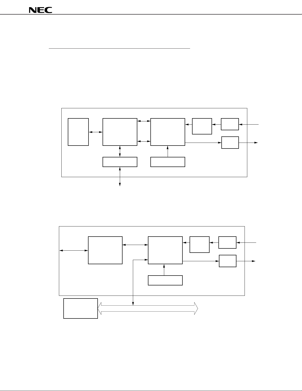
The followings are examples of the terminal equipment and the ATM Hub application using the µPD98402A.
NIC APPLICATION
DATA I/F (UTOPIA)
CONTROL
MEMORY
PD98401A
m
SAR CHIP
CNT I/F
PD98402A
m
PHY CHIP
155.52MHz
CLOCK
RECOVERY
CHIP
Rx PMD
TO HUB
Tx PMD
HOST BUS I/F
SWITCH
SYSTEM
SYNTHESIZER
HOST BUS
HUB APPLICATION (NIC SIDE)
DATA I/F
(UTOPIA)
CNT I/F
PD98402A
m
PHY CHIP
SYNTHESIZER
155.52MHz
CLOCK
RECOVERY
CHIP
Rx PMD
TO NIC
Tx PMD
CONTROLLER BUSCONTROLLER
3

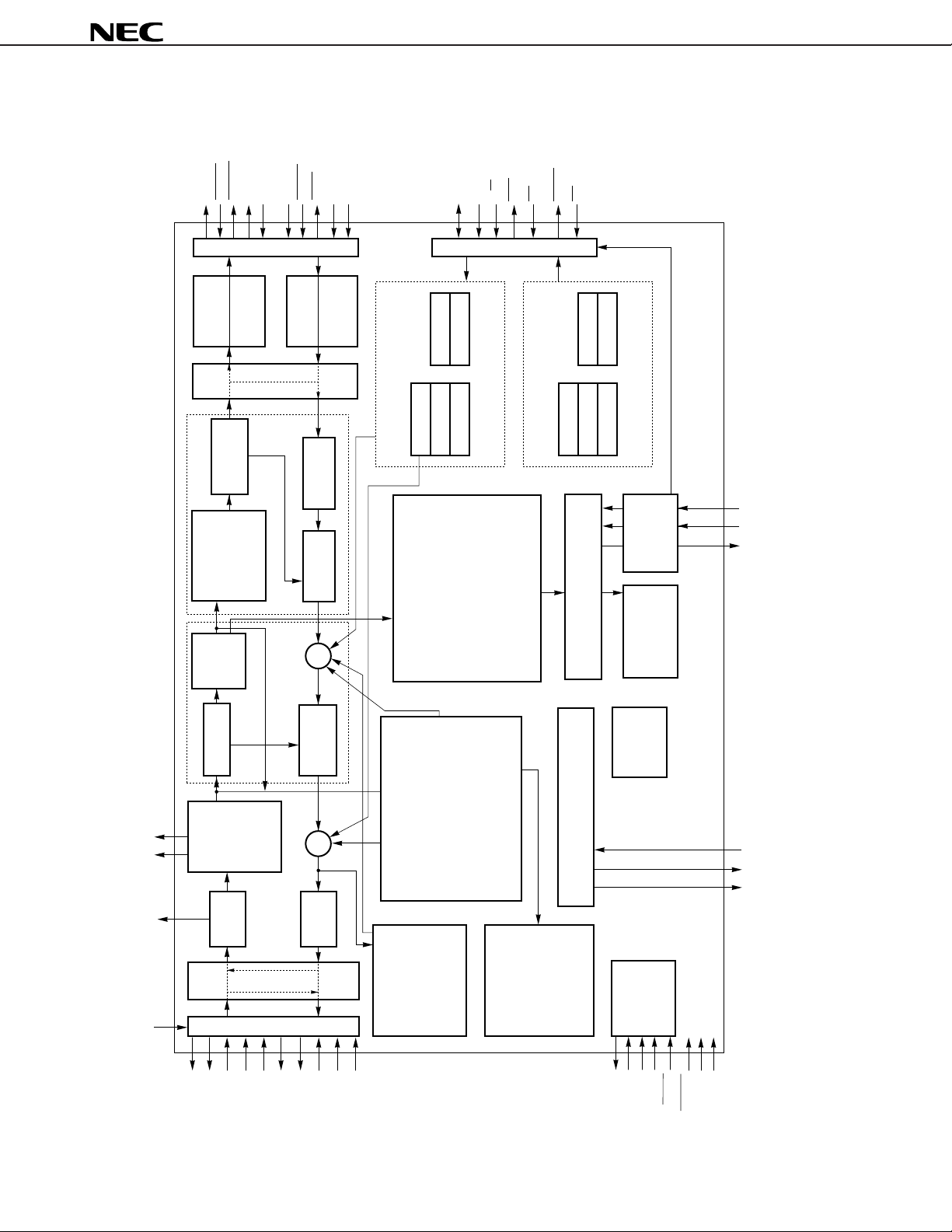
BLOCK DIAGRAM
RDO0—RDO7
RENBL
EMPTY
RSOC
RCLK
TDI0—TDI7
TENBL
FULL
TSOC
TCLK
D0—D7
A0—A5
R/W
ACK
CEOEPHINT
µ
PD98402A
ATM Layer Interface
Rx FIFO
4 Cell
Idle Cell
Drop
Loop Back
Cell
Descrambler
Cell Delineation
HEC Verification
HEC Correction
Generator
Rx Timing
Tx FIFO
4 Cell
HEC
Generator
Cell
Scrambler
+
Idle Cell
Insert
Management Interface
F2
C2
F1
Tx Overhead Registers
K2
C1(#1~#3)
Rx Overhead
Controller
F2
C2
F1
Rx Overhead Registers
K2
C1(#1~#3)
INT Cause
Registers
OAM Sequencer
Performance
Registers
RAL
TAL
LOS
Mode
Register
TFSS
TCL
TxFP
RxFP
OOF
RCL
Descrambler
A1, A2
SONET
Framing
Parallel
Serialfi
Scrambler
+
Parallel
fiSerial
Tx Overhead
Controller
Tx Timing Generator
Loop Back
BIP
Generator
PSEL
PMD Interface
RDIC, RDIT
TFKC, TFKT
TCOC, TCOT
TDOC, TDOT
TPC
TPD0-TPD7
RCIC, RCIT
TFC
RPC
RPD0-RPD7
(Tx)
BIP
Generator
(Rx)
TDO
Test
TJI
Block
TCK
TMS
TRST
DD
V
RESET
GND
4

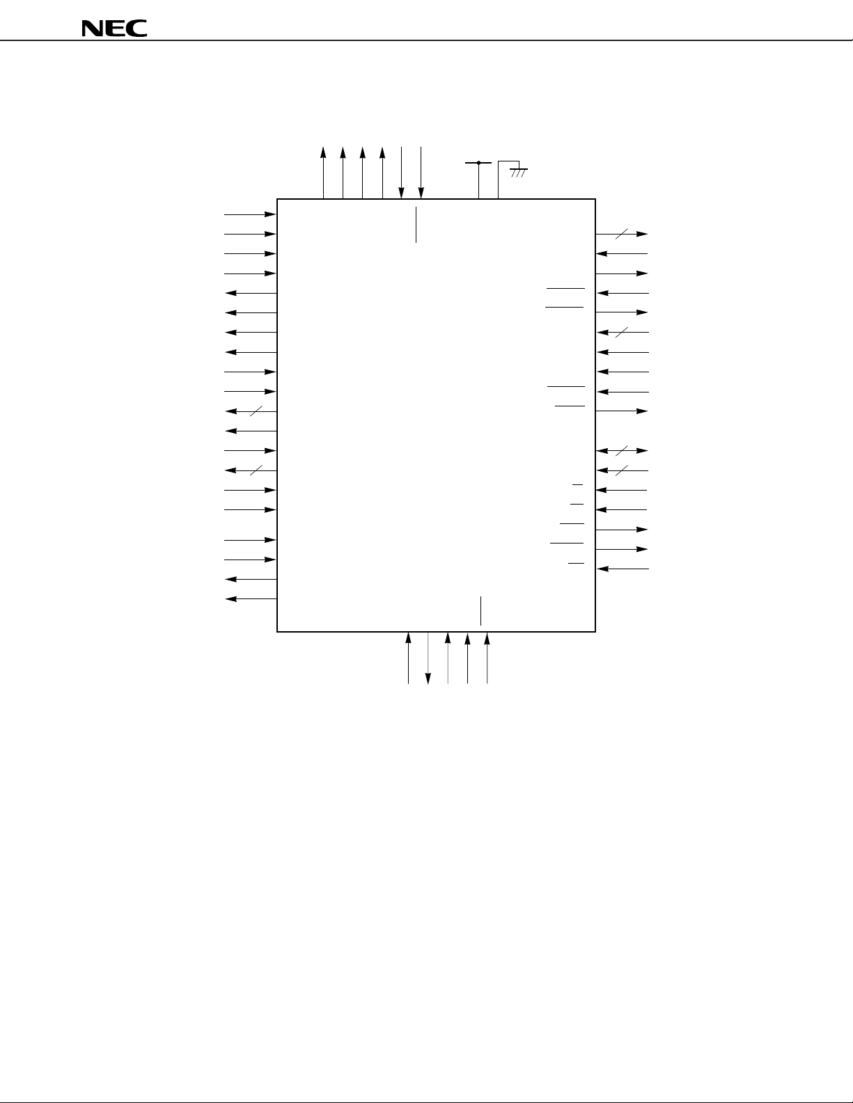
FUNCTIONAL PIN GROUPS
Control
µ
PD98402A
PMD
Interface
OAM
Interface
8
8
RDIC
RDIT
RCIC
RCIT
TDOC
TDOT
TCOC
TCOT
TFKC
TFKT
TPD0-TPD7
TPC
TFC
RPD0-RPD7
RPC
PSEL
RAL
TAL
LOS
OOF
RCL
TCL
TxFP
RxFP
TFSS
TJI
RESET
TDO
TCK
TMS
DD
V
TRST
GND
RDO0-RDO7
TDI0-TDI7
RCLK
RSOC
RENBL
EMPTY
TCLK
TSOC
TENBL
FULL
D0-D7
A0-A5
R/W
CE
ACK
PHINT
OE
8
ATM Layer
8
8
6
Interface
Management
Interface
Note
JTAG boundary scan
pin
Note This function can be supported at the customer’s request.
5

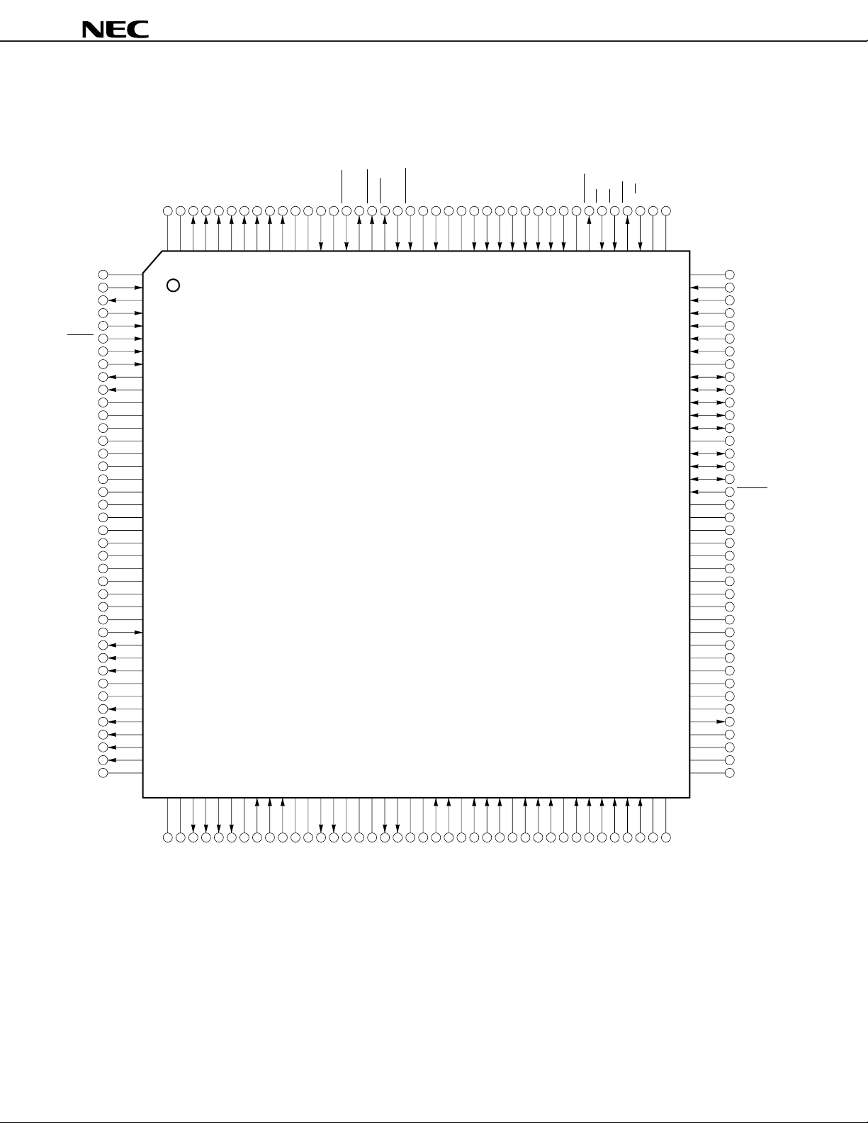
PIN CONFIGURATION
160-pin plastic QFP (FINE PITCH) (24 × 24 mm) (Top View)
µ
PD98402A
V
TCK
TDO
TJI
TMS
TRST
RAL
TAL
LOS
OOF
IC
IC
IC
IC
IC
IC
IC
IC
IC
V
GND
IC
IC
IC
IC
IC
IC
IC
TFSS
RxFP
TxFP
TCL
V
GND
TPD0
TPD1
TPD2
TPD3
TPD4
V
GND
GND
RDO7
RDO6
RDO5
RDO4
RDO3
RDO2
RDO1
DD
RDO0
V
GND
RCLK
GND
RENBL
RSOC
EMPTY
FULL
TSOC
TEMBL
GND
TCLK
GND
VDDTDI7
TDI6
TDI5
TDI4
TDI3
TDI2
TDI1
TDI0
GND
PHINTCEOE
ACK
R/W
GND
GND
121122123124125126127128129130131132133134135136137138139140141142143144145146147148149150151152153154155156157158159160
V
DD
1
2
3
4
5
6
7
8
9
10
11
12
13
14
15
16
µ
PD98402AGM-KED
17
18
19
DD
20
21
22
23
24
25
26
27
28
29
30
31
32
DD
33
34
35
36
37
38
39
DD
40
120
119
118
117
116
115
114
113
112
111
110
109
108
107
106
105
104
103
102
101
100
99
98
97
96
95
94
93
92
91
90
89
88
87
86
85
84
83
82
81
DD
A5
A4
A3
A2
A1
A0
GND
D7
D6
D5
D4
D3
GND
D2
D1
D0
RESET
CG
GND
DD
V
IC
IC
IC
IC
IC
GND
IC
IC
IC
IC
IC
IC
IC
IC
RCL
IC
IC
IC
DD
V
807978777675747372717069686766656462616059585756555453525150494847464544434241 63
GND
GND
TPD5
TPD6
TPC
TPD7
GND
TFC
TFKT
TFKC
GND
V
TCOT
TCOC
GND
V
DD
DD
DD
V
Remarks 1. IC : Internally Connected. Leave open.
2. CG : Connect to GND.
6
TDOT
TDOC
DD
V
GND
RCIT
RCIC
GND
RDIT
RPC
RDIC
GND
RPD7
RPD6
GND
RPD5
RPD4
RPD3
RPD2
RPD1
PSEL
RPD0
GND
GND

A0-A5 : Address Bus
ACK : Read/write Cycle Receive Acknowledge
CE : Chip Enable
D0–D7 : Data Bus
EMPTY : Output Buffer Empty
FULL : Buffer Full
GND : Ground
LOS : Loss of Signal
OE : Output Enable
OOF : Out of Frame
PHINT : Physical Interrupt
PSEL : PMD I/F Select
RAL : Receive Alarm
RCIC : Receive Clock Input Complement
RCIT : Receive Clock Input True
RCL : Internal Receive System Clock
RCLK : Receive Data Transferring Clock from the ATM Layer Device
RDIC : Receive Data Input Complement
RDIT : Receive Data Input True
RDO0-RDO7 : Receive Data Output
RENBL : Receive Data Enable
RESET : System Reset
RPC : Receive Parallel Data Clock
RPD0-RPD7 : Receive Parallel Data
RSOC : Receive Start Address of ATM Cell
R/W : Read/write Control
RxFP : Receive Frame Pulse
TAL : Transmit Alarm
TCK : Test Clock
TCL : Internal Transmit System Clock
TCLK : Transmit Data Transferring Clock from the ATM Layer Device
TCOC : Transmit Clock Output Complement
TCOT : Transmit Clock Output True
TDI0-TDI7 : Transmit Data Input from the ATM Layer
TDO : Test Data Output
TDOC : Transmit Data Output Complement
TDOT : Transmit Data Output True
TENBL : Transmit Data Enable
TFC : Transmit Reference Clock
TFKC : Transmit Reference Clock Complement
TFKT : Transmit Reference Clock True
TFSS : Transmit Frame Set Signal
TJI : Test JTAG Data Input
TPC : Transmit Parallel Data Clock
TPD0-TPD7 : Transmit Parallel Data
TMS : Test Mode Select
TRST : Test Reset
TSOC : Transmit Start Address of ATM Cell
TxFP : Transmit Frame Pulse
DD : Supply Voltage
V
µ
PD98402A
7

µ
PD98402A
1. PIN FUNCTIONS
• PMD Interface
Symbol Pin No. I/O I/O Level Function
RDIC 66 I Pseudo ECL These pins are used to input receive serial data when serial
Complement (–) interface mode is used (PSEL pin input = low level). Ground
RDIT 65 I Pseudo ECL
True (+)
RCIC 63 I Pseudo ECL These pins are used to input the receive system clock when
Complement (–) serial interface mode is used (PSEL pin input = low level).
RCIT 62 I Pseudo ECL
True (+)
TDOC 59 O Pseudo ECL These pins are used to output transmit serial data when serial
Complement (–) interface mode is used (PSEL pin input = low level). They are
TDOT 58 O Pseudo ECL
True (+)
TCOC 54 O Pseudo ECL These pins are used to output transmit clocks when serial
Complement (–) interface mode is used (PSEL pin input = low level). Transmit
TCOT 53 O Pseudo ECL
True (+)
TFKC 50 I Pseudo ECL These pins are used to input transmit system clocks when
Complement (–) serial interface mode is used (PSEL pin input = low level).
TFKT 49 I Pseudo ECL
True (+)
them when Parallel interface mode is used.
Clocks are input in synchronization with receive data. Ground
them when parallel interface mode is used.
open-drain pins. Terminate them with VDD –2 V via a 50 Ω
resistor. To be undefined after reset.
clocks to be input to the TFKC/TFKT pins are output passing
through internal gates. They are open-drain pins. Terminate
them with VDD –2 via a 50 Ω resistor. To be undefined after
reset.
Transmit data output from the TDOC/TDOT pins is output in
synchronization with clocks that are input to these pins.
Ground them when parallel interface mode is used.
RPD0-RPD7 77-73, 71-69 I TTL These pins are used to input receive parallel data when
parallel interface mode is used (PSEL pin input = high level).
Leave them open when serial interface mode is used.
RPC 67 I TTL This pin is used to input the receive system clock when
parallel interface mode is used (PSEL pin input = high level).
Input clocks synchronous with the receive data. Leave it open
when serial interface mode is used.
TPD0-TPD7 35-39, 43-45 O CMOS These pins are used to output transmit parallel data when
parallel interface mode is used (PSEL pin input = high level).
Leave them open when serial interface mode is used.
TPC 46 O CMOS This pin is used to output transmit clocks when parallel
interface mode is used (PSEL pin input = high level). Transmit
clocks to be input to the TFC pin are output passing through
internal gates. Leave it open when serial interface mode is
used.
TFC 48 I TTL This pins is used to input transmit system clocks when parallel
interface mode is used (PSEL pin input = high level). Transmit
data output from pins TPD0 to TPD7 are output in
synchronization with the clocks input to this pin. Leave it open
when serial interface mode is used.
PSEL 78 I CMOS This pin is used to select the mode for PMD interface serial/
parallel interface.
Low level: Serial interface mode
High level: Parallel interface mode
8
 Loading...