

DATA SHEET
MOS INTEGRATED CIRCUIT
µ
PD784915B, 784916B
16-BIT SINGLE-CHIP MICROCONTROLLERS
DESCRIPTION
The µPD784915B, 784916B are members of the NEC 78K/IV Series of microcontrollers equipped with a high-
speed 16-bit CPU and are versions with improved electrical characteristics of the
µ
PD784915 Subseries.
This series contains many peripheral hardware units ideal for VCR control, such as a multi-function timer unit
(super timer unit) suitable for software servo control and VCR analog circuits.
A one-time PROM version of the
µ
PD784916B, the µPD78P4916, is also available.
µ
PD784915A, 784916A of the
Detailed function descriptions are provided in the following user’s manuals. Be sure to read them before
designing.
µ
PD784915 Subseries User’s Manual - Hardware: U10444E
78K/IV Series User’s Manual - Instruction: U10905E
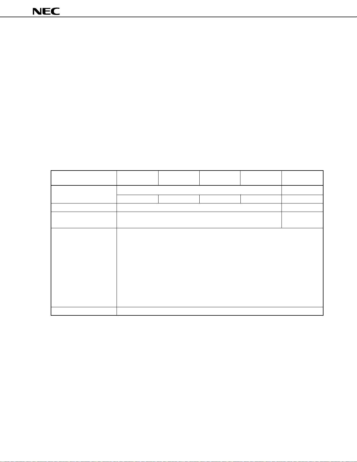
FEATURES
• High instruction execution speed realized by 16-bit CPU core
• Minimum instruction execution time: 250 ns (with 8-MHz internal clock)
• High internal memory capacity
Part Number ROM RAM
µ
PD784915B 49152 bytes 1280 bytes
µ
PD784916B 63488 bytes
• VCR analog circuits conforming to VHS Standard
• CTL amplifier
• RECCTL driver (rewritable)
• CFG amplifier
• DFG amplifier
• DPG comparator
• DPFG separation circuit (ternary separation circuit)
• Reel FG comparator (2 channels)
• CSYNC comparator
• Timer unit (super timer unit) for servo control
• Serial interface: 2 channels (3-wire serial I/O)
• A/D converter: 12 channels (conversion time: 10
• Low-frequency oscillation mode: main system clock frequency = internal clock frequency
• Low-power dissipation mode: CPU can operate with a subsystem clock.
• Supply voltage range: V
• Hardware watch function: watch operation at low voltage (VDD = 2.7 V (MIN.)) and low current
DD = 2.7 to 5.5 V
µ
s)
APPLICATIONS
Control system/servo/timer of VCR
Unless mentioned otherwise, the µPD784916B is described as the representative product.
Document No. U13118EJ1V0DS00 (1st edition)
Date Published January 1998 N CP(K)
Printed in Japan
The information in this document is subject to change without notice
©
1996
1998
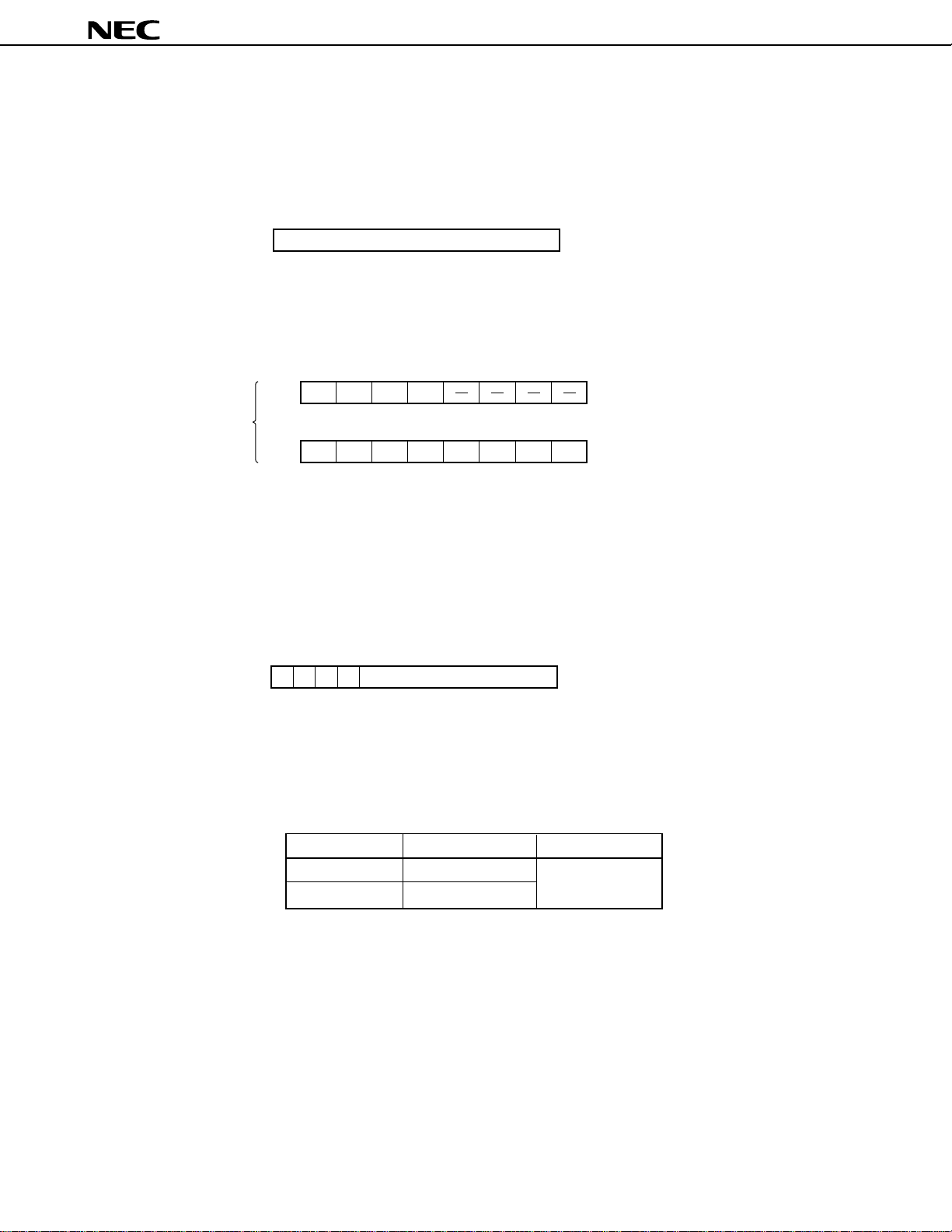
ORDERING INFORMATION
Part Number Package
µ
PD784915BGF-xxx-3BA 100-pin plastic QFP (14 x 20 mm)
µ
PD784916BGF-xxx-3BA 100-pin plastic QFP (14 x 20 mm)
Remark xxx indicates ROM code suffix.
Product Development of 78K/IV Series
: Under mass production
: Under development
2
I
C bus supported
PD784038Y
µ
Standard
PD784026
µ
Enhanced A/D,
16-bit timer,
and power
management
PD784038
µ
Internal memory capacity was enhanced
Pin compatible with PD784026
µ
PD784216Y
µ
PD784216
100-pin
I/O and internal memory capacity
was enhanced
µ
µ
PD784915B, 784916B
Multimaster I2C bus supported
PD784225Y
µ
PD784225
µ
80-pin,
ROM correction was enhanced
Multimaster I2C bus supportedMultimaster I2C bus supported
PD784218Y
µ
PD784218
µ
Internal memory capacity was enhanced
ROM correction was added
ASSP
µ
PD784955
DC inverter control
PD784908
µ
On-chip IEBus
Controller
µ
PD78F4943
For CD-ROM,
56 Kbytes of flash memory
PD784915
µ
On-chip software servo control
VCR analog circuit, enhanced timer
TM
Multimaster I2C bus supported
µ
PD784054
PD784046
µ
On-chip 10-bit A/D
PD784928Y
µ
PD784928
µ
Function of the PD784915 was
enhanced
µ
2
Function List (1/2)
µ
PD784915B, 784916B
Item
Internal ROM capacity
Internal RAM capacity
Operating clock
Minimum instruction
execution time
I/O ports
Real-time output port
Super Timer/counter
timer
unit
Capture register
VCR special
circuit
General-purpose
timer
PWM output
Serial interface
A/D converter
µ
PD784915B
49152 bytes 63488 bytes
1280 bytes
16 MHz (internal clock: 8 MHz)
Low frequency oscillation mode: 8 MHz (internal clock: 8 MHz)
Low power dissipation mode: 32.768 kHz (subsystem clock)
250 ns (with 8-MHz internal system clock)
input : 8
54
I/O : 46
11 (including one each for pseudo VSYNC, head amplifier switch, and chrominance rotation)
Timer/counter Compare register Capture register Remark
TM0 (16 bits) 3 TM1 (16 bits) 3 1
FRC (22 bits) - 6
TM3 (16 bits) 2 1
UDC (5 bits) 1 -
EC (8 bits) 4 - For HSW signal generation
EDV (8 bits) 1 - For CFG signal division
Input signal Number of bits Measurable cycle Operating edge
CFG 22 125 ns to 524 ms ↑↓
DFG 22 125 ns to 524 ms ↑
HSW 16 1 µs to 65.5 ms ↑↓
VSYNC 22 125 ns to 524 ms ↑
CTL 16 1 µs to 65.5 ms ↑↓
TREEL 22 125 ns to 524 ms ↑↓
SREEL 22 125 ns to 524 ms ↑↓
•VSYNC separation circuit, HSYNC separation circuit
• VISS detection, wide aspect detection circuits
• Field identification circuit
• Head amplifier switch/chroma rotation output circuit
Timer Compare register Capture register
TM2 (16 bits) 1 —
TM4 (16 bits) 1 (capture/compare) 1
TM5 (16 bits) 1 —
• 16-bit accuracy : 3 channels (carrier frequency: 62.5 kHz)
• 8-bit accuracy : 3 channels (carrier frequency: 62.5 kHz)
3-wire serial I/O: 2 channels
• BUSY/STRB control (1 channel only)
8-bit resolution × 12 channels, conversion time: 10 µs
µ
PD784916B
3
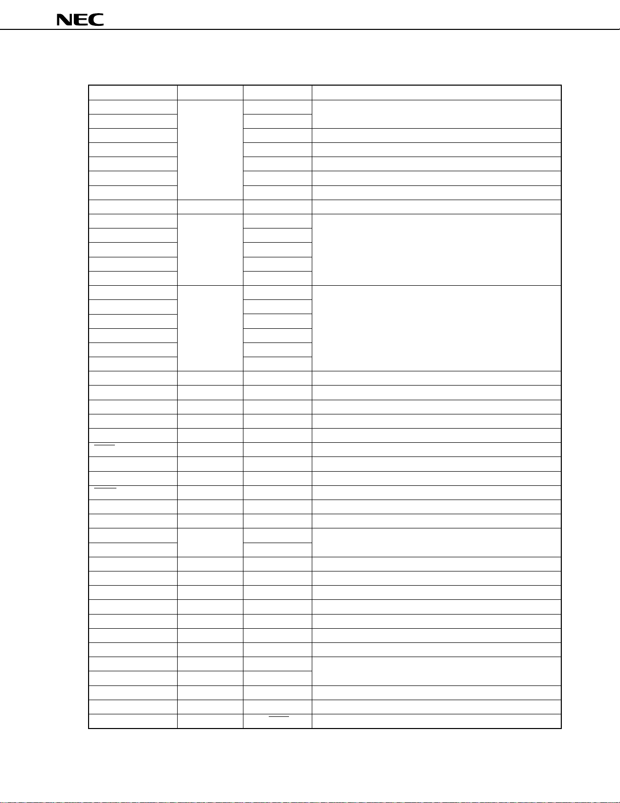
Function List (2/2)
µ
PD784915B, 784916B
Item
Analog circuit
Interrupt
External
Internal
Standby function
Watch function
Supply voltage
Package
µ
PD784915B
• CTL amplifier
• RECCTL driver (rewritable)
• DFG amplifier, DPG comparator, CFG amplifier
• DPFG separation circuit (ternary separation circuit)
• Reel FG comparator (2 channels)
• CSYNC comparator
4 levels (programmable), vector interrupt, macro service, context switching
9 (including NMI)
19 (including software interrupt)
HALT/STOP mode/low power dissipation mode/low power dissipation HALT mode
STOP mode can be released by input of valid edge of NMI pin, watch interrupt (INTW), or
INTP1/INTP2/KEY0-KEY4 pins
0.5-second measurement, low-voltage operation (VDD = 2.7 V)
VDD = 2.7 to 5.5 V
100-pin plastic QFP (14 × 20 mm)
µ
PD784916B
4
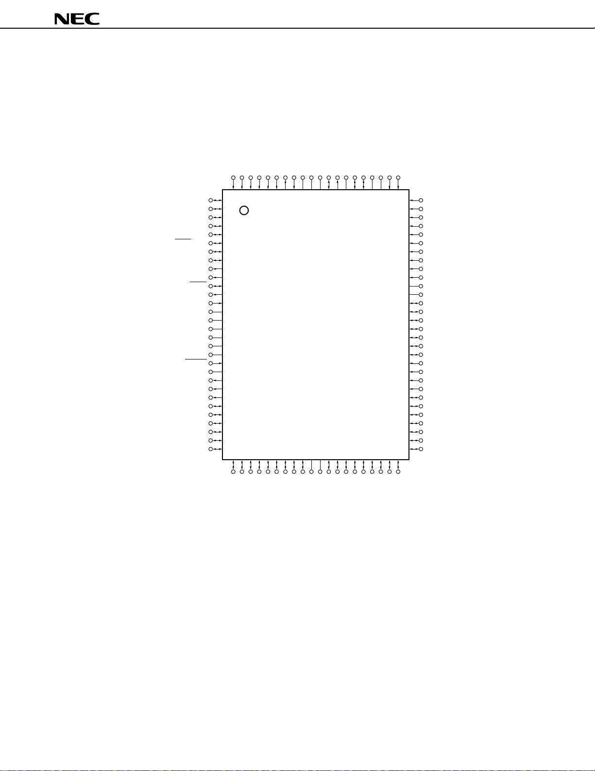
PIN CONFIGURATION (Top View)
• 100-pin plastic QFP (14 x 20 mm)
µ
PD784915BGF-xxx-3BA
µ
PD784916BGF-xxx-3BA
100
1
P64
V
XT1
XT2
V
X2
X1
2
3
4
5
6
7
8
9
10
11
12
13
DD
14
15
16
SS
17
18
19
20
IC
21
22
23
24
25
26
27
28
29
30
3132333435363738 39 40 41 42 4344454647484950
P65/HWIN
P66/PWM4
P67/PWM5
P60/STRB/CLO
P61/SCK1/BUZ
P62/SO1
P63/SI1
PWM0
PWM1
SCK2
SO2
SI2/BUSY
RESET
PTO02
PTO01
PTO00
P87/PTO11
P86/PTO10
P85/PWM3
P84/PWM2
P83/ROTC
P82/HASW
CSYNCIN
REEL0IN/INTP3
REEL1IN
DFGIN96DPGIN95CFGCPIN
99
98
97
CFGAMPO
CFGIN92AV
94
93
DD1
SS1
AV
91
90
VREFC89CTLOUT2
CTLOUT1
CTLIN86RECCTL
88
87
-
RECTTL+
85
84
µ
PD784915B, 784916B
SS2
CTLDLY83AV
ANI1181ANI10
82
80
ANI9
79
ANI8
78
P77/ANI7
77
P76/ANI6
76
P75/ANI5
75
P74/ANI4
74
P73/ANI3
73
P72/ANI2
72
P71/ANI1
71
P70/ANI0
70
69
68
67
66
65
64
63
62
61
60
59
58
57
56
55
54
53
52
51
REF
AV
AV
DD2
P96
P95/KEY4
P94/KEY3
P93/KEY2
P92/KEY1
P91/KEY0
P90/ENV
NMI
INTP0
INTP1
INTP2
P00
P01
P02
P03
P04
P05
P06
SS
DD
V
P80
P57
P56
P55
P54
P53
P52
P51
P50
V
P47
P46
P45
P44
Caution Directly connect the IC (Internally Connected) pin to V
P43
P42
SS.
P41
P40
P07
5

µ
PD784915B, 784916B
ANI0-ANI11 : Analog Input P00-P07 : Port0
AVDD1, AVDD2 : Analog Power Supply P40-P47 : Port4
AV
SS1, AVSS2 : Analog Ground P50-P57 : Port5
AVREF : Analog Reference Voltage P60-P67 : Port6
BUSY : Serial Busy P70-P77 : Port7
BUZ : Buzzer Output P80, P82-P87 : Port8
CFGAMPO : Capstan FG Amplifier Output P90-P96 : Port9
CFGCPIN : Capstan FG Capacitor Input PTO00-PTO02 : Programmable Timer Output
CFGIN : Analog Unit Input PTO10, PTO11
CLO : Clock Output PWM0-PWM5 : Pulse Width Modulation Output
CSYNCIN : Analog Unit Input RECCTL+, RECCTL– : RECCTL Output/PBCLT Input
CTLDLY : Control Delay Input REEL0IN, REEL1IN : Analog Unit Input
CTLIN : CTL Amplifier Input Capacitor RESET : Reset
CTLOUT1, CTLOUT2 : CTL Amplifier Output ROTC : Chrominance Rotate Output
DFGIN : Analog Unit Input SCK1, SCK2 : Serial Clock
DPGIN : Analog Unit Input SI1, SI2 : Serial Input
ENV : Envelope Input SO1, SO2 : Serial Output
HASW : Head Amplifier Switch Output STRB : Serial Strobe
HWIN : Hardware Timer External Input V
IC : Internally Connected VREFC : Reference Amplifier Capacitor
INTP0-INTP3 : Interrupt From Peripherals V
KEY0-KEY4 : Key Return X1, X2 : Crystal (Main System Clock)
NMI : Nonmaskable Interrupt XT1, XT2 : Crystal (Subsystem Clock)
DD : Power Supply
SS : Ground
6
INTERNAL BLOCK DIAGRAM
µ
PD784915B, 784916B
NMI
INTP0 to INTP3
PWM0 to PWM5
PTO00 to PTO02
PTO10, PTO11
VREFC
REEL0IN
REEL1IN
CSYNCIN
DFGIN
DPGIN
CFGIN
CFGAMPO
CFGCPIN
CTLOUT1
CTLOUT2
CTLIN
RECCTL+
RECCTL
CTLDLY
AVDD1, AVDD2
AVSS1, AVSS2
AVREF
ANI0 to ANI1
SI1
SO1
SCK1
INTERRUPT
SUPER TIMER
ANALOG UNIT
A/D CONVERTER
INTERFACE 1
CONTROL
UNIT
&
SERIAL
78K/IV
16-bit CPU CORE
(RAM: 512 bytes)
RAM
768 bytes
ROM
VDD
VSS
SYSTEM
CONTROL
CLOCK OUTPUT
BUZZER OUTPUT
KEY INPUT
REAL-TIME
OUTPUT PORT
PORT0 P00 to P07
PORT4 P40 to P47
PORT5 P50 to P57
PORT6 P60 to P67
PORT7 P70 to P77
X1
X2
XT1
XT2
RESET
CLO
BUZ
KEY0 to KEY4
P00 to P07
P80, P82, P83
SI2/BUSY
SO2
SCK2
STRB
SERIAL
INTERFACE 2
Remark Internal ROM capacity depends on the product.
PORT8 P80, P82 to P87
PORT9 P90 to P96
7
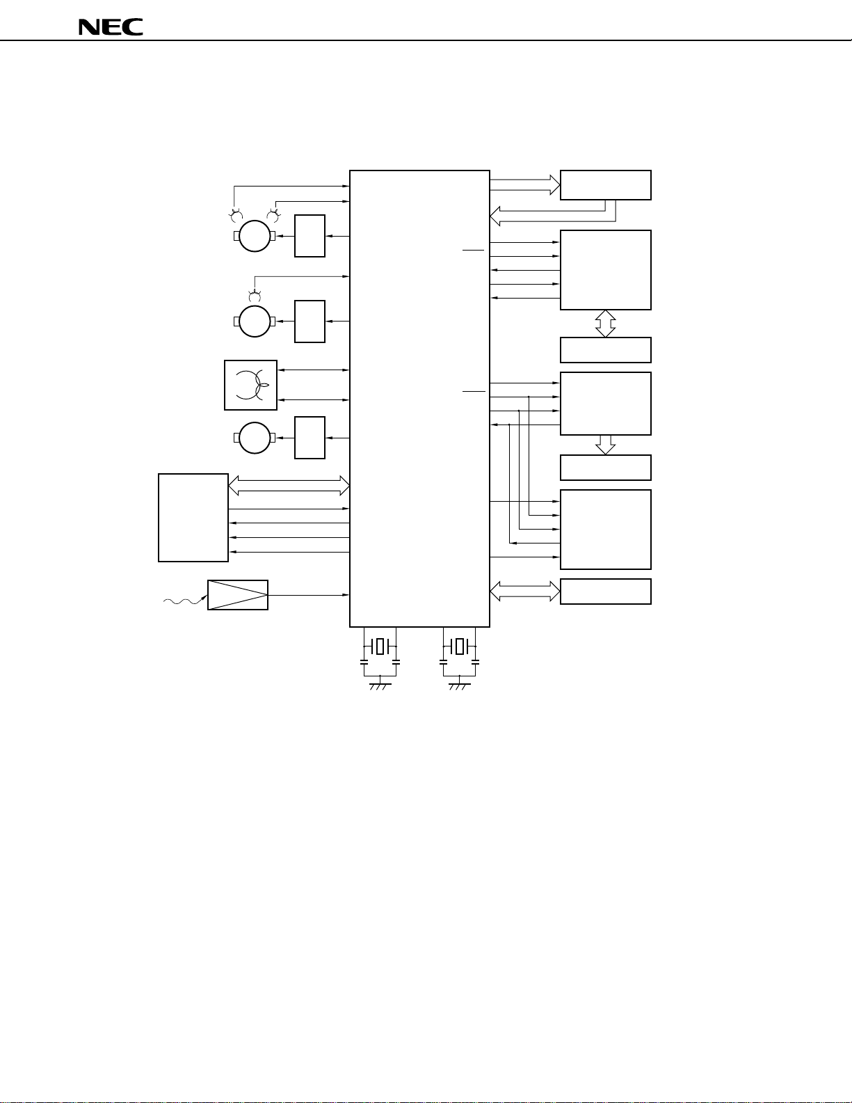
SYSTEM CONFIGURATION EXAMPLE
• Camera-contained VCR
Drum motor M
Capstan motor M
CTL head
Loading motor M
Driver
Driver
Driver
DFG
DPG
CFG
DFGIN
DPGIN
PWM0
CFGIN
PWM1
RECCTL+
RECCTL
PWM2
µ
PD784916B
-
PORT
PORT
PORT
SCK1
SI1
SO1
INTP0
PORT
SCK2
SO2
BUSY
µ
PD784915B, 784916B
Key matrix
INTP0
Camera-
SCK
controlling
SO
microcontroller
SI
PD784036
µ
PORT
Camera block
CS
CLK
LCD C/D
µ
PD7225
DATA
BUSY
Audio/video
signal
processing
circuit
Remote
controller
signal
Composite sync signal
Video head switch
Audio head switch
Pseudo vertical sync signal
Remote controller
reception signal
µ
PC2800A
PORT
CSYNCIN
PTO00
PTO01
P80
INTP2
XT1 XT2X1 X2
16 MHz 32.768 kHz
PORT
STRB
PORT
LCD display panel
CS
CLK
OSD
DATA
µ
PD6461
BUSY
STB
Mechanical block
8
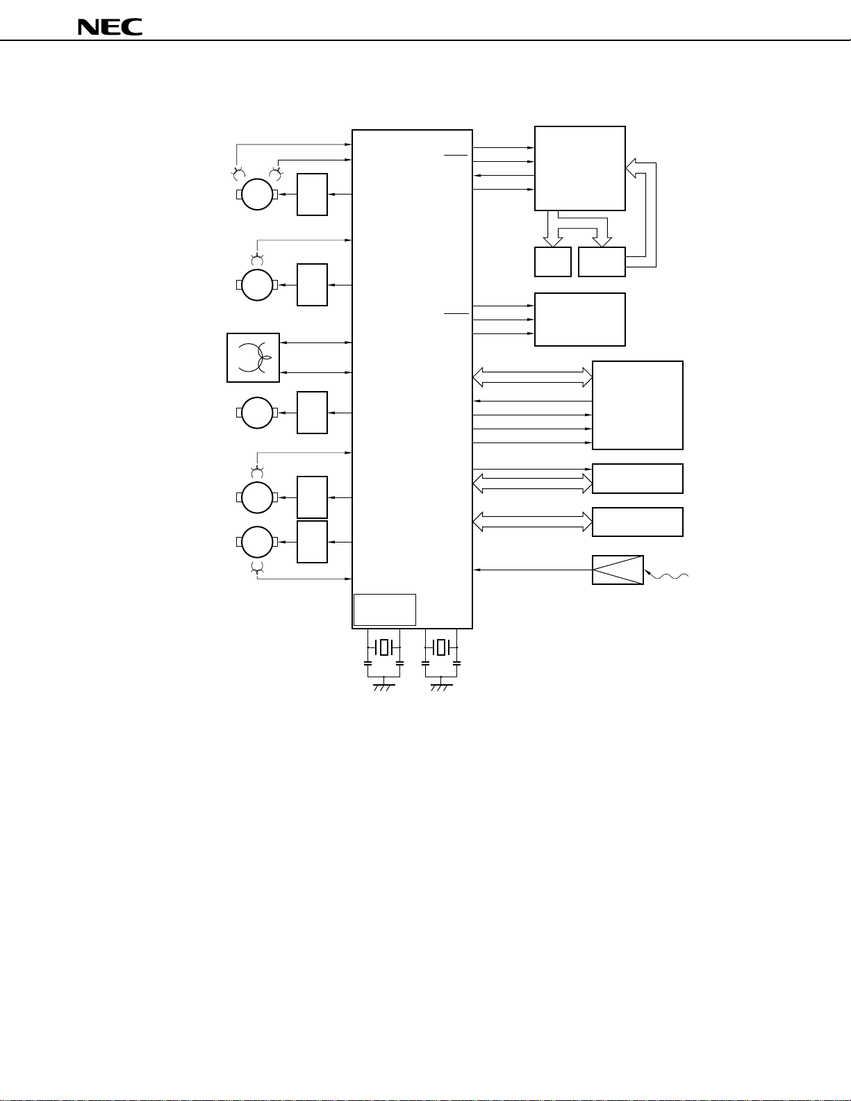
• Stationary VCR
Drum motor M
Capstan motor M
CTL head
Loading motor M
Reel motor
µ
PD784915B, 784916B
µ
PD784916B
DFG
DFGIN
DPGIN
DPG
Driver
Driver
Driver
Reel FG0
M
M
Driver
Driver
Reel FG1
PWM0
CFG
CFGIN
PWM1
RECCTL+
RECCTL
PWM2
REEL0IN
PWM3
PWM4
REEL1IN
Low frequency
oscillation mode
-
CSYNCIN
PTO00
PTO01
PWM5
XT1 XT2X1 X2
PORT
SCK1
SI1
SO1
PORT
SCK2
SO2
PORT
Composite sync signal
Video head switch
Audio head switch
Pseudo vertical sync signal
P80
PORT
PORT
Remote controller
INTP2
reception signal
STB
CLK
DOUT
DIN
FIP
CS
CLK
DATA
TM
C/D
FIP
µ
PD16311
Key matrix
OSD
µ
PD6464
Audio/video signal
processing circuit
Mechanical block
µ
PC2800A
Tuner
Remote controller
signal
8 MHz 32.768 kHz
9

µ
PD784915B, 784916B
CONTENTS
1. DIFFERENCES AMONG µPD784915 SUBSERIES PRODUCTS .................................................. 11
2. PIN FUNCTIONS.............................................................................................................................. 12
2.1 Port Pins ................................................................................................................................................ 12
2.2 Non-Port Pins ........................................................................................................................................ 13
2.3 I/O Circuits and Connection of Unused Pins...................................................................................... 15
3. INTERNAL BLOCK FUNCTIONS.................................................................................................... 19
3.1 CPU Registers ....................................................................................................................................... 19
3.1.1 General-purpose registers ......................................................................................................... 19
3.1.2 Other CPU registers.................................................................................................................... 20
3.2 Memory Space....................................................................................................................................... 20
3.3 Special Function Registers (SFRs) ..................................................................................................... 23
3.4 Ports ....................................................................................................................................................... 28
3.5 Real-time Output Port ........................................................................................................................... 29
3.6 Super Timer Unit ................................................................................................................................... 33
3.7 Serial Interface ...................................................................................................................................... 38
3.8 A/D Converter ........................................................................................................................................ 40
3.9 VCR Analog Circuits ............................................................................................................................. 41
3.10 Watch Function ..................................................................................................................................... 47
3.11 Clock Output Function ......................................................................................................................... 48
4. INTERNAL/EXTERNAL CONTROL FUNCTION............................................................................ 49
4.1 Interrupt Function ................................................................................................................................. 49
4.1.1 Vector interrupt ........................................................................................................................... 51
4.1.2 Context switching ....................................................................................................................... 51
4.1.3 Macro service .............................................................................................................................. 52
4.1.4 Application example of macro service .....................................................................................54
4.2 Standby Function.................................................................................................................................. 57
4.3 Clock Generator Circuit........................................................................................................................ 59
4.4 Reset Function ...................................................................................................................................... 60
5. INSTRUCTION SETS....................................................................................................................... 61
6. ELECTRICAL CHARACTERISTICS ............................................................................................... 65
7. PACKAGE DRAWING ..................................................................................................................... 77
8. RECOMMENDED SOLDERING CONDITIONS............................................................................... 78
APPENDIX A. DEVELOPMENT TOOLS ............................................................................................... 79
APPENDIX B. RELATED DOCUMENTS ............................................................................................... 81
10
µ
PD784915B, 784916B
1. DIFFERENCES AMONG µPD784915 SUBSERIES PRODUCTS
The µPD784915 Subseries consists of the six products listed in Table 1-1. The µPD784915A is a low-cost process-
shrinked version of the µPD784915. The µPD784916A expands the internal ROM capacity of the µPD784915 to 62
µ
Kbytes. The
and 784916A.
The µPD78P4916 features writable one-time PROM instead of the mask ROM of the µPD784915, 784915A,
784916A, 784915B, and 784916B. Except for this substitution of PROM for ROM and the fact that PROM capacity
differs from the ROM capacities offered in the other products, the
products.
In switching from the PROM product, used for debugging and testing application systems, to the mask ROM
products for mass production, be careful to check the differences among these products.
For details on the CPU functions and the internal hardware, refer to
Hardware (U10444E).
PD784915B and 784916B feature improved electrical characteristics compared to the µPD784915A
µ
PD78P4916 has the same functions as those
µ
PD784915 Subseries User’s Manual —
µ
Table 1-1. Differences among
PD784915 Subseries Products
Item
Internal ROM Mask ROM
Internal RAM 1280 bytes 2048 bytes
Internal memory capacity Not provided Provided
selection register (IMS)
Electrical characteristics The electrical characteristics of the µPD784915A/784916A, the µPD784915B/784916B,
Pin connections In the µPD78P4916, pin function for PROM read/write has been added.
µ
PD784915,
784915A
49152 bytes 63488 bytes 49152 bytes 63488 bytes 63232 bytes
and the µPD78P4916 differ with respect to the items listed below.
• P40 to P47, P50 to P57: Low-level input voltage
• VDD supply current
• Data hold current
• CTL amplifier: Phase signal elimination ratio
• CFG amplifier: CFGAMPO low-level output current
For details, refer to the data sheet of each product.
• µPD784915A/784916A Data Sheet (U11022J)
• µPD784915B/784916B Data Sheet (This document)
• µPD78P4916 Data Sheet (U11045J)
µ
PD784916A
µ
PD784915B
µ
PD784916B
µ
PD78P4916
Note
Note
Note The internal PROM and internal RAM capacities can be changed using the internal memory selection register
(IMS).
Caution The PROM version and mask ROM version differ in noise immunity and noise radiation, etc. When
considering replacing a PROM version with a mask ROM version when switching from preproduction
to volume production, perform sufficient evaluation using a CS version (not ES version) of the
mask ROM version.
11
2. PIN FUNCTIONS
2.1 Port Pins
µ
PD784915B, 784916B
Pin Name I/O
P00 to P07 I/O Real-time 8-bit I/O port (port 0).
P40 to P47 I/O
P50 to P57 I/O
P60 I/O STRB/CLO 8-bit I/O port (port 6).
P61 SCK1/BUZ • Can be set in input or output mode in 1-bit units.
P62 SO1 • Can be connected with software pull-up resistors.
P63 SI1
P64
P65 HWIN
P66 PWM4
P67 PWM5
P70 to P77 Input ANI0 to ANI7 8-bit input port (port 7)
P80 I/O Real-time Pseudo VSYNC output 7-bit I/O port (port 8).
P82 output port HASW output • Can be set in input or output mode in
P83 ROTC output • Can be connected with software pull-
P84 PWM2
P85 PWM3
P86 PTO10
P87 PTO11
P90 I/O ENV 7-bit I/O port (port 9).
P91 to P95 KEY0 to KEY4 • Can be set in input or output mode in 1-bit units.
P96
Alternate Function
output port • Can be set in input or output mode in 1-bit units.
• Can be connected with software pull-up resistors.
-
-
-
-
8-bit I/O port (port 4).
• Can be set in input or output mode in 1-bit units.
• Can be connected with software pull-up resistors.
8-bit I/O port (port 5).
• Can be set in input or output mode in 1-bit units.
• Can be connected with software pull-up resistors.
• Can be connected with software pull-up resistors.
Function
1-bit units.
up resistors.
12
2.2 Non-Port Pins (1/2)
µ
PD784915B, 784916B
Pin Name I/O
REEL0IN Input INTP3 Reel FG input
REEL1IN
DFGIN
DPGIN
CFGIN
CSYNCIN
CFGCPIN
CFGAMPO Output
PTO00 Output
PTO01
PTO02
PTO10 P86
PTO11 P87
PWM0 Output
PWM1
PWM2 P84
PWM3 P85
PWM4 P66
PWM5 P67
HASW Output P82 Head amplifier switch signal output
ROTC Output P83 Chroma rotation signal output
ENV Input P90 Envelope signal input
SI1 Input P63 Serial data input (serial interface channel 1)
SO1 Output P62 Serial data output (serial interface channel 1)
SCK1 I/O P61/BUZ Serial clock I/O (serial interface channel 1)
SI2 Input BUSY Serial data input (serial interface channel 2)
SO2 Output
SCK2 I/O
BUSY Input SI2 Serial busy signal input (serial interface channel 2)
STRB Output P60/CLO Serial strobe signal output (serial interface channel 2)
ANI0 to ANI7 Analog input P70 to P77 Analog signal input of A/D converter
ANI8 to ANI11
CTLIN
CTLOUT1 Output
CTLOUT2 I/O
RECCTL+, RECCTL– I/O
CTLDLY
VREFC
NMI Input
INTP0 to INTP2 Input
INTP3 Input REEL0IN
KEY0 to KEY4 Input P91 to P95 Key input signal input
CLO Output P60/STRB Clock output
BUZ Output P61/SCK1 Buzzer output
--
--
--
Alternate Function
-
-
-
-
-
-
-
-
-
-
-
-
-
-
-
-
-
-
-
-
Function
Drum FG, PFG input (ternary)
Drum PG input
Capstan FG input
Composite SYNC input
CFG comparator input
CFG amplifier output
Programmable timer output of super timer unit
PWM output of super timer unit
Serial data output (serial interface channel 2)
Serial clock I/O (serial interface channel 2)
CTL amplifier input capacitor connection
CTL amplifier output
Logic signal input/CTL amplifier output
RECCTL signal output/PBCTL signal input
External time constant connection (for RECCTL rewriting)
VREF amplifier AC connection
Non-maskable interrupt request input
External interrupt request input
13
2.2 Non-Port Pins (2/2)
µ
PD784915B, 784916B
Pin Name I/O
HWIN Input P65 External input of hardware watch counter
RESET Input
X1 Input
X2
XT1 Input
XT2
AVDD1, AVDD2
AVSS1, AVSS2
AVREF
VDD
VSS
IC
-
-
--
--
--
--
--
--
Alternate Function
-
-
-
Function
Reset input
Crystal connection for main system clock oscillation
Crystal connection for subsystem clock oscillation.
Crystal connection for watch clock oscillation
Positive power supply to analog circuits
GND of analog circuits
Reference voltage input to A/D converter
Positive power supply to digital circuits
GND of digital circuits
Internally connected. Directly connect to VSS.
14
µ
PD784915B, 784916B
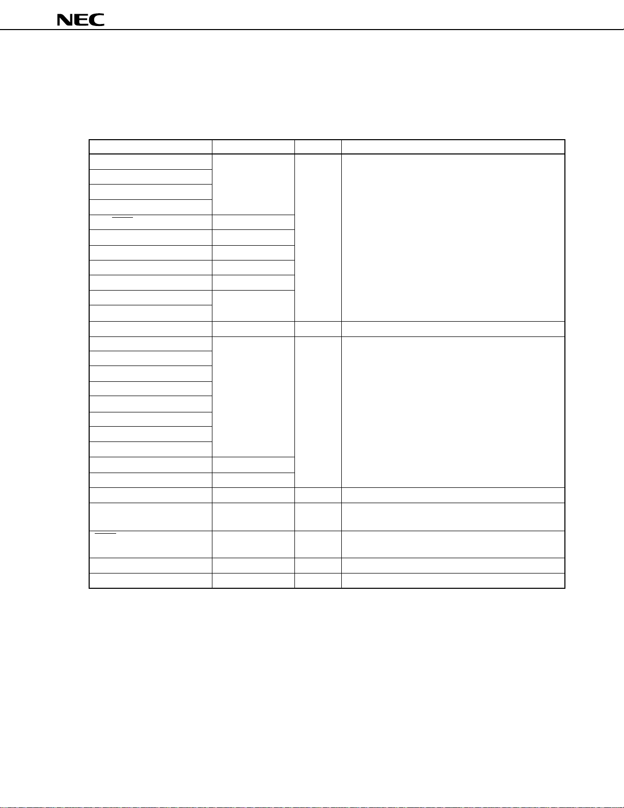
2.3 I/O Circuits and Connection of Unused Pins
Table 2-1 shows the I/O circuit type of each pin and the recommended connection of unused pins. For the
configuration of each type of I/O circuit, refer to Figure 2-1.
Table 2-1. I/O Circuit Type of each Pin and Recommended Connection of Unused Pins (1/2)
Pin I/O Circuit Type I/O Recommended Connection of Unused Pins
P00 to P07 5-A I/O Input: Connect to VDD
P40 to P47
P50 to P57
P60/STRB/CLO
P61/SCK1/BUZ 8-A
P62/SO1 5-A
P63/SI1 8-A
P64 5-A
P65/HWIN 8-A
P66/PWM4 5-A
P67/PWM5
P70/ANI0 to P77/ANI7 9 Input Connect to VSS
P80 5-A I/O Input: Connect to VDD
P82/HASW
P83/ROTC
P84/PWM2
P85/PWM3
P86/PTO10
P87/PTO11
P90/ENV
P91/KEY0 to P95/KEY4 8-A
P96 5-A
SI2/BUSY 2-A Input Connect to VDD
SO2 4 Output Hi-Z: Connect to VSS via a pull-down resistor
SCK2 8-A I/O Input: Connect to VDD
ANI8 to ANI11 7 Input Connect to VSS
RECCTL+, RECCTL– — I/O When ENCTL = 0 and ENREC = 0: Connect to VSS
Output: Leave open
Output: Leave open
Others: Leave open
Output: Leave open
Remark ENCTL : bit 1 of amplifier control register (AMPC)
ENREC: bit 7 of amplifier mode register 0 (AMPM0)
15
µ
PD784915B, 784916B
Table 2-1. I/O Circuit Type of each Pin and Recommended Connection of Unused Pins (2/2)
Pin I/O Circuit Type I/O Recommended Connection of Unused Pins
DFGIN — Input When ENDRUM = 0: Connect to VSS
DPGIN When ENDRUM = 0 or ENDRUM = 1 and SELPGSEPA
= 0: Connect to VSS
CFGIN, CFGCPIN When ENCAP = 0: Connect to VSS
CSYNCIN When ENCSYN = 0: Connect to VSS
REEL0IN/INTP3, REEL1IN When ENREEL = 0: Connect to VSS
CTLOUT1 — Output Leave open
CTLOUT2 — I/O When ENCTL = 0 and ENCOMP = 0: Connect to VSS
When ENCTL = 1: Leave open
CFGAMPO — Output Leave open
CTLIN — — When ENCTL = 0: Leave open
VREFC When ENCTL = 0 and ENCAP = 0 and ENCOMP = 0:
Leave open
CTLDLY Leave open
PWM0, PWM1 3 Output Leave open
PTO00 to PTO02
NMI 2 Input Connect to VDD
INTP0 Connect to VDD or VSS
INTP1, INTP2 2-A Input Connect to VDD
AVDD1, AVDD2 — — Connect to VDD
AVREF, AVSS1, AVSS2 Connect to VSS
RESET 2 — —
XT1 — — Connect to VSS
XT2 Leave open
IC Directly connect to VSS
Remark ENDRUM : bit 2 of amplifier control register (AMPC)
SELPGSEPA : bit 2 of amplifier mode register 0 (AMPM0)
ENCAP : bit 3 of amplifier control register (AMPC)
ENCSYN : bit 5 of amplifier control register (AMPC)
ENREEL : bit 6 of amplifier control register (AMPC)
ENCTL : bit 1 of amplifier control register (AMPC)
ENCOMP : bit 4 of amplifier control register (AMPC)
16
Figure 2-1. I/O Circuits of Pins (1/2)
µ
PD784915B, 784916B
Type 2
IN
Schmitt trigger input with hysteresis characteristics
Type 2-A
V
DD
P-ch
pullup
enable
IN
Schmitt trigger input with hysteresis characteristics
Type 3
DD
V
P-ch
data
N-ch
OUT
Type 5-A
pullup
enable
data
output
disable
input
enable
Type 7
IN
P-ch
N-ch
DD
V
P-ch
N-ch
Comparator
+
-
V
P-ch
DD
IN/
OUT
Type 4
DD
data
output
disable
Push-pull output that can make output high
impedance (both P-ch and N-ch are off)
V
P-ch
N-ch
OUT
Type 8-A
pullup
enable
data
output
disable
V
REF
(threshold voltage)
DD
V
P-ch
N-ch
V
P-ch
DD
IN/
OUT
17
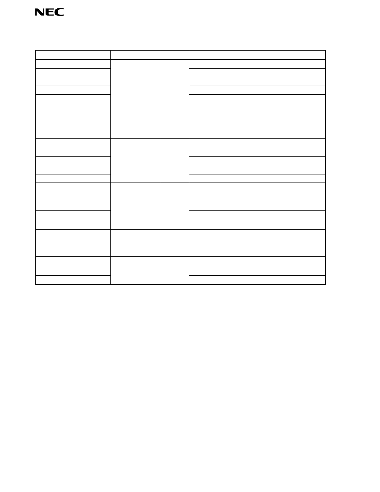
Type 9
Figure 2-1. I/O Circuits of Pins (2/2)
µ
PD784915B, 784916B
P-ch
IN
N-ch
V
Comparator
+
-
REF
(threshold voltage)
input enable
18
µ
PD784915B, 784916B
3. INTERNAL BLOCK FUNCTIONS
3.1 CPU Registers
3.1.1 General-purpose registers
µ
PD784916B has eight banks of general-purpose registers. One bank consists of sixteen 8-bit general-
The
purpose registers. Two of these 8-bit registers can be used in pairs as a 16-bit register. Four of the 16-bit generalpurpose registers can be used to specify a 24-bit address in combination with an 8-bit address expansion register.
These eight banks of general-purpose registers can be selected by software or context switching function.
The general-purpose registers, except for the address expansion registers V, U, T, and W, are mapped to the
internal RAM.
Figure 3-1. Configuration of General-Purpose Registers
A (R1) X (R0)
AX (RP0)
B (R3) C (R2)
BC (RP1)
R5 R4
RP2
R7 R6
RP3
R9 R8V
VP (RP4)
VVP (RG4)
R11 R10U
UP (RP5)
UUP (RG5)
D (R13) E (R12)T
DE (RP6)
TDE (RG6)
H (R15) L (R14)W
HL (RP7)
WHL (RG7)
( ): absolute name
8 banks
Caution Although R4, R5, R6, R7, RP2, and RP3 can be used as X, A, C, B, AX, and BC registers,
respectively, by setting the RSS bit of PSW to 1, do not use this function. The function of the
RSS bit is planned to be deleted from the future models in the 78K/IV Series.
19
µ
PD784915B, 784916B
3.1.2 Other CPU registers
(1) Program counter
µ
The program counter of the
PD784916B is 20 bits wide. The value of the program counter is automatically
updated as the program is executed.
19 0
PC
(2) Program status word
This is a register that holds the various statuses of the CPU. Its contents are automatically updated as the program
is executed.
12 11 10 9 8
PSWH UF15RBS214RBS113RBS0
PSW
PSWL S7Z
6
RSS
5AC4IE3
Note
0
P/V201CY
Note The RSS flag is provided to maintain compatibility with the microcontrollers in the 78K/III Series. Always
set this flag to 0 except when the software of the 78K/III Series is used.
(3) Stack pointer
This is a 24-bit pointer that holds the first address of the stack.
Be sure to write 0 to the high-order 4 bits.
23 0
SP
000200
3.2 Memory Space
The µPD784916B can access a 64 Kbyte memory space.
Table 3-1 shows the addresses of the internal ROM and internal data areas.
Table 3-1. Memory Space
Part Number Internal ROM Area Internal Data Area
µ
PD784915B 0000H-BFFFH FA00H-FFFFH
µ
PD784916B 0000H-F7FFH
Caution Some products in the 78K/IV Series can access up to 1 Mbyte of memory space in an address
expansion mode which is set by the LOCATION instruction. However, the memory space of the
µ
PD784916B is 64 Kbytes (0000H to FFFFH). Therefore, be sure to execute the LOCATION 0
instruction immediately after reset to set the memory space to 64 Kbytes (the LOCATION
instruction cannot be used more than twice).
20
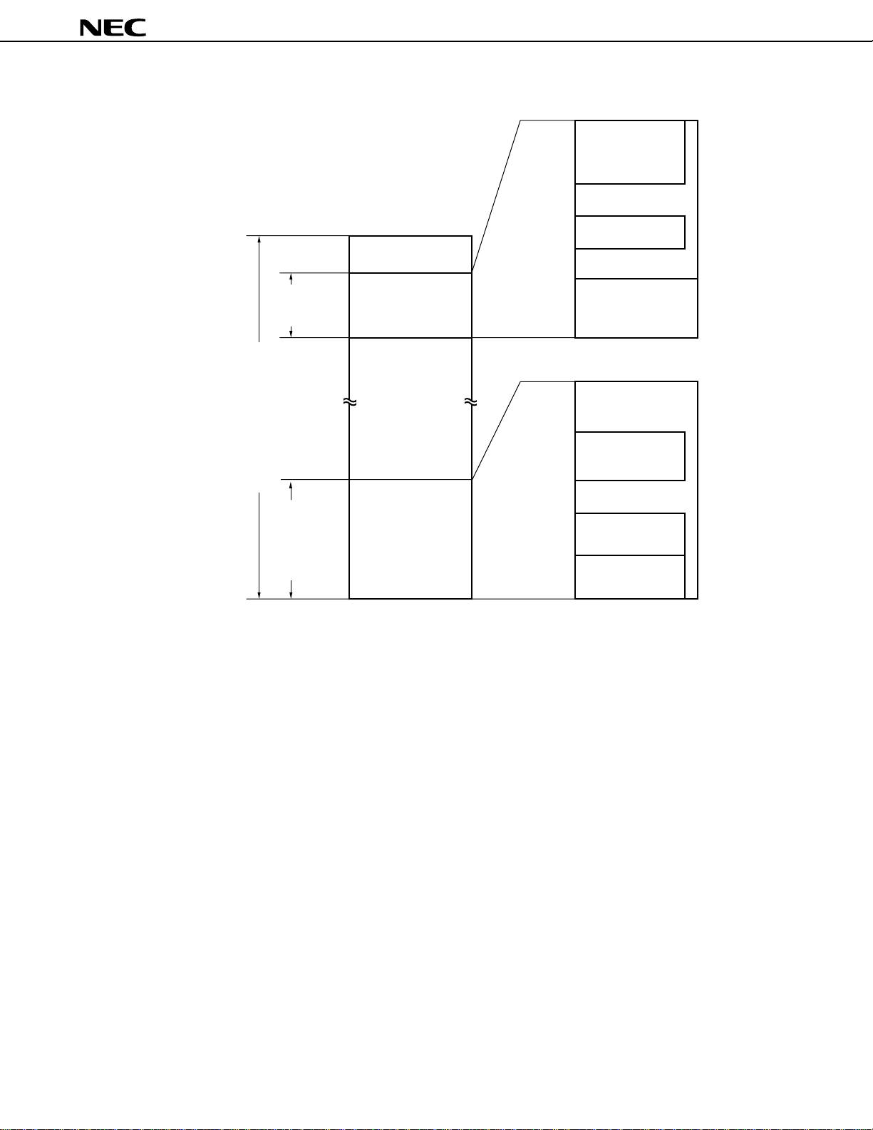
µ
Figure 3-2. Memory Map of µPD784915B
FEFFH
FE80H
FE7FH
PD784915B, 784916B
General-purpose
registers (128 bytes)
FFFFH
FF00H
FEFFH
Data
memory
FA00H
F9FFH
Memory space (64 Kbytes)
C000H
BFFFH
data memory
Program memory/
Special function register
(SFR) (256 bytes)
Internal RAM
(1280 bytes)
Cannot be used
Internal ROM
(49152 bytes)
0000H
FE3BH
FE06H
FD00H
FCFFH
FA00H
BFFFH
1000H
0FFFH
0800H
07FFH
0080H
007FH
0040H
003FH
0000H
Macro service control
word area (54 bytes)
Data area (512 bytes)
Program/data area
(768 bytes)
Program/data area
(49152 bytes)
CALLF entry area
(2048 bytes)
CALLT table area
(64 bytes)
Vector table area
(64 bytes)
21
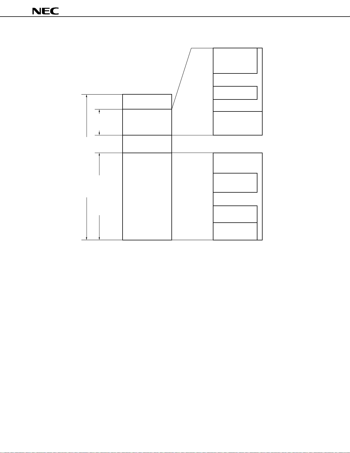
Figure 3-3. Memory Map of µPD784916B
FEFFH
FE80H
FE7FH
µ
PD784915B, 784916B
General-purpose
registers (128 bytes)
FFFFH
FEFFH
Data
memory
FA00H
F9FFH
F7FFH
Memory space (64 Kbytes)
data memory
Program memory/
Special function register
FF00H
F800H
0000H
(SFR) (256 bytes)
Internal RAM
(1280 bytes)
Cannot be used
Internal ROM
(63488 bytes)
FE3BH
FE06H
FD00H
FCFFH
FA00H
F7FFH
1000H
0FFFH
0800H
07FFH
0080H
007FH
0040H
003FH
0000H
Macro service control
word area (54 bytes)
Data area (512 bytes)
Program/data area
(768 bytes)
Program/data area
(63488 bytes)
CALLF entry area
(2048 bytes)
CALLT table area
(64 bytes)
Vector table area
(64 bytes)
22

µ
PD784915B, 784916B
3.3 Special Function Registers (SFRs)
Special function registers are assigned special functions and mapped to a 256-byte space from addresses FF00H
through FFFFH. These registers include mode registers and control registers that control the internal peripheral
hardware units.
Caution Do not access an address to which no SFR is assigned. If such an address is accessed by
µ
mistake, the
Table 3-2 lists the special function registers (SFRs). The meanings of the symbols in this table are as follows:
• Abbreviation............................ Abbreviation of an SFR. This abbreviation is reserved for NEC’s assembler
• R/W ......................................... Indicates whether the SFR in question can be read or written.
PD784916B may be deadlocked. This deadlock can be cleared only by reset input.
(RA78K4). With a C compiler (CC78K4), the abbreviation can be used as an sfr
variable by the #pragma sfr instruction.
R/W : Read/write
R : Read only
W : Write only
• Bit length ................................. Indicates the bit length (word length) of the SFR.
• Bit units for manipulation ....... Indicates bit units in which the SFR in question can be manipulated. An SFR that
can be manipulated in 16-bit units can be described as the operand sfrp of an
instruction. Specify an even address to manipulate this SFR.
An SFR that can be manipulated in 1-bit units can be described for a bit
manipulation instruction.
• After reset ............................... Indicates the status of each register after the RESET signal has been input.
23
µ
PD784915B, 784916B
Table 3-2. Special Function Registers (1/4)
Bit Bit Units for After
Address Special Function Register (SFR) Name Symbol R/W Length Manipulation Releasing
1 bit 8 bits 16 bits Reset
FF00H Port 0 P0 R/W 8 √√
FF04H Port 4 P4 8 √√
FF05H Port 5 P5 8 √√
FF06H Port 6 P6 8 √√
FF07H Port 7 P7 R 8 √√
FF08H Port 8 P8 R/W 8 √√
FF09H Port 9 P9 8 √√
FF0EH Port 0 buffer register L P0L 8 √√
FF0FH Port 0 buffer register H P0H 8 √√
FF10H Timer 0 compare register 0 CR00 16
FF11H Event counter compare register 0 ECC0 W 8
FF12H Timer 0 compare register 1 CR01 R/W 16
FF13H Event counter compare register 1 ECC1 W 8
FF14H Timer 0 compare register 2 CR02 R/W 16
FF15H Event counter compare register 2 ECC2 W 8
FF16H Timer 1 compare register 0 CR10 R/W 16
FF17H Event counter compare register 3 ECC3 W 8
FF18H Timer 1 compare register 1 CR11 R/W 16
FF1AH Timer 1 compare register 2 CR12 R 16
FF1CH Timer 1 compare register 3 CR13 R/W 16
FF1EH Timer 2 compare register 0 CR20 16
FF20H Port 0 mode register PM0 W 8
FF24H Port 4 mode register PM4 8
FF25H Port 5 mode register PM5 8
FF26H Port 6 mode register PM6 8
FF28H Port 8 mode register PM8 8
FF29H Port 9 mode register PM9 8
FF2EH Real-time output port 0 control register RTPC R/W 8 √√
FF30H Timer register 0 TM0 R 16
FF31H Event counter EC R/W 8
FF32H Timer register 1 TM1 R 16
FF34H Free running counter (bits 0 to 15) FRCL 16
FF35H Free running counter (bits 16 to 21) FRCH 8
FF36H Timer register 2 TM2 16
FF38H Timer control register 0 TMC0 R/W 8 √√
FF39H Timer control register 1 TMC1 8 √√
FF3AH Timer control register 2 TMC2 8 √√
FF3BH Timer control register 3 TMC3 8 √√
--
-
--
-
--
-
--
-
--
--
--
--
-
-
-
-
-
-
--
-
--
--
-
--
√
√
√
√
√
√
√
√
√
√
√
√
-
Undefined
-
-
-
-
-
-
-
√ Cleared to 0
-
√
-
√
-
√
-
√
√
√
√
-
-
-
-
-
-
√ Cleared to 0
-
√
√ 0000H
√ Cleared to 0
-
-
-
-
FFH
FDH
7FH
00H
00H
00H
00×00000
Remark Cleared to 0: Counter is initialized to 0 within 16 clocks after the reset signal has been deasserted (the
contents before initialization are undefined).
24
µ
PD784915B, 784916B
Table 3-2. Special Function Registers (2/4)
Bit Bit Units for After
Address Special Function Register (SFR) Name Symbol R/W Length Manipulation Releasing
1 bit 8 bits 16 bits Reset
FF3CH Timer register 3 TM3 R 16
FF3DH Timer control register 4 TMC4 R/W 8 √√
FF3EH Timer register 4 TM4 R 16
FF48H Port 8 mode control register PMC8 R/W 8 √√
FF4DH Trigger source select register TRGS0 8 √√
FF4EH Pull-up resistor option register L PUOL 8 √√
FF4FH Pull-up resistor option register H PUOH 8 √√
FF50H Input control register ICR 8 √√
FF51H Up/down counter count register UDC 8
FF52H Event divider counter EDV R 8
FF53H Capture mode register CPTM R/W 8 √√
FF54H Timer register 5 TM5 R 16
FF56H Timer 3 capture register 0 CPT30 16
FF58H Timer 0 output mode register TOM0 W 8
FF59H Timer 0 output control register TOC0 8
ADML
Note 1
Note 2
R/W 8
8 √√
FF5AH Timer 1 output mode register TOM1
FF5BH Timer 1 output control register TOC1 W 8
FF5CH Timer 3 compare register 0 CR30 R/W 16
FF5EH Timer 3 compare register 1 CR31 16
FF60H Port 8 buffer register L P8L 8 √√
FF63H Up/down counter compare register UDCC W 8
FF65H Trigger source select register 1 TRGS1 R/W 8 √√
FF66H Port 6 mode control register PMC6 8 √√
FF68H A/D converter mode register ADM 16
FF6AH A/D conversion result register ADCR R 8
FF6CH Hardware watch counter 0 HW0 R/W 16
FF6EH Hardware watch counter 1 HW1 R 16
FF6FH Watch mode register WM R/W 8 √√
FF70H PWM control register 0 PWMC0 R/W 8 √√
FF71H PWM control register 1 PWMC1 8 √√
FF72H PWM0 modulo register PWM0 16
FF73H PWM2 modulo register PWM2 8
FF74H PWM1 modulo register PWM1 16
FF75H PWM3 modulo register PWM3 8
--
--
-
-
--
--
-
-
-
-
--
--
-
--
-
--
--
--
-
--
-
√ Cleared to 0
-
××000000
√ Cleared to 0
-
-
-
-
-
√
√
√
√
√
√
√
√
√
√
-
-
-
√ Cleared to 0
√
-
-
-
-
√ Cleared to 0
√
-
-
-
√ 0000H
-
-
√ Not affected
√ by reset
-
-
√ 0000H
√ 0000H
-
00H
10H
Undefined
Cleared to 0
00H
××000000
00H
80H
00H
000×0×0×
Undefined
00H
Undefined
00××0×00
05H
15H
00H
00H
Notes 1. When the timer 1 output mode register (TOM1) is read, the write sequence of the REC driver is read
(bits 0 and 1).
2. ADML is the low-order 8 bits of the A/D converter mode register (ADM) and can be manipulated in 1or 8-bit units.
Remark Cleared to 0: Counter is initialized to 0 within 16 clocks after the reset signal has been deasserted (the
contents before initialization are undefined).
25
µ
PD784915B, 784916B
Table 3-2. Special Function Registers (3/4)
Bit Bit Units for After
Address Special Function Register (SFR) Name Symbol R/W Length Manipulation Releasing
1 bit 8 bits 16 bits Reset
FF76H PWM5 modulo register PWM5 R/W 16
FF77H PWM4 modulo register PWM4 8
FF78H Event divider control register EDVC W 8
FF79H Clock output mode register CLOM R/W 8 √√
FF7AH Timer 4 capture/compare register 0 CR40 16
FF7BH Clock control register CC 8 √√
FF7CH Timer 4 capture register 1 CR41 R 16
FF7DH Capture/compare control register CRC W 8
FF7EH Timer 5 compare register CR50 R/W 16
FF84H Serial mode register 1 CSIM1 8 √√
FF85H Serial shift register 1 SIO1 8
FF88H Serial mode register 2 CSIM2 8 √√
FF89H Serial shift register 2 SIO2 8
FF8AH Serial control register 2 CSIC2 8
FF91H Head amplifier switch output control register HAPC 8 √√
FF94H Amplifier control register AMPC 8 √√
FF95H Amplifier mode register 0 AMPM0 8 √√
FF96H Amplifier mode register 1 AMPM1 8 √√
FF97H Gain control register CTLM 8 √√
FFA0H External interrupt mode register INTM0 8 √√
FFA1H External capture mode register 1 INTM1 8 √√
FFA2H External capture mode register 2 INTM2 8 √√
FFA6H Key interrupt control register KEYC 8 √√
FFA8H In-service priority register ISPR R 8 √√
FFAAH Interrupt mode control register IMC R/W 8 √√
FFACH Interrupt mask flag register MK0L 8 √√√ FFH
FFADH MK0H 8 √√
FFAEH MK1L 8 √√√
FFAFH MK1H 8 √√
FFB0H FRC capture register 0L CPT0L R 16
FFB1H FRC capture register 0H CPT0H 8
FFB2H FRC capture register 1L CPT1L 16
FFB3H FRC capture register 1H CPT1H 8
FFB4H FRC capture register 2L CPT2L 16
FFB5H FRC capture register 2H CPT2H 8
FFB6H FRC capture register 3L CPT3L 16
FFB7H FRC capture register 3H CPT3H 8
FFB8H FRC capture register 4L CPT4L 16
MK0
MK1
--
-
-
--
--
-
--
-
-
-
--
-
--
-
--
-
--
-
--
√ 0000H
√
√
√
√
√
√
√
√
√
√
-
-
√ Cleared to 0
√ Cleared to 0
√ Cleared to 0
-
-
-
-
-
-
-
-
-
-
-
-
-
-
-
-
√ Cleared to 0
-
√
-
√
-
√
-
√
00H
00H
00H
00H
00H
00H
Undefined
00H
Undefined
00H
000000×0
00H
70H
00H
80H
Remark Cleared to 0: Counter is initialized to 0 within 16 clocks after the reset signal has been deasserted (the
contents before initialization are undefined).
26

µ
PD784915B, 784916B
Table 3-2. Special Function Registers (4/4)
Bit Bit Units for After
Address Special Function Register (SFR) Name Symbol R/W Length Manipulation Releasing
1 bit 8 bits 16 bits Reset
FFB9H FRC capture register 4H CPT4H R 8
FFBAH FRC capture register 5L CPT5L 16
FFBBH FRC capture register 5H CPT5H 8
FFC0H Standby control register STBC R/W 8
FFC4H Execution speed select register MM W 8
FFCEH CPU clock status register PCS R 8 √√
FFCFH
FFE0H Interrupt control register (INTP0) PIC0 R/W 8 √√
FFE1H Interrupt control register (INTCPT3) CPTIC3 8 √√
FFE2H Interrupt control register (INTCPT2) CPTIC2 8 √√
FFE3H Interrupt control register (INTCR12) CRIC12 8 √√
FFE4H Interrupt control register (INTCR00) CRIC00 8 √√
FFE5H Interrupt control register (INTCLR1) CLRIC1 8 √√
FFE6H Interrupt control register (INTCR10) CRIC10 8 √√
FFE7H Interrupt control register (INTCR01) CRIC01 8 √√
FFE8H Interrupt control register (INTCR02) CRIC02 8 √√
FFE9H Interrupt control register (INTCR11) CRIC11 8 √√
FFEAH Interrupt control register (INTCPT1) CPTIC1 8 √√
FFEBH Interrupt control register (INTCR20) CRIC20 8 √√
FFEDH Interrupt control register (INTTB) TBIC 8 √√
FFEEH Interrupt control register (INTAD) ADIC 8 √√
FFEFH Interrupt control register (INTP2)
FFF0H Interrupt control register (INTUDC) UDCIC 8 √√
FFF1H Interrupt control register (INTCR30) CRIC30 8 √√
FFF2H Interrupt control register (INTCR50) CRIC50 8 √√
FFF3H Interrupt control register (INTCR13) CRIC13 8 √√
FFF4H Interrupt control register (INTCSI1) CSIIC1 8 √√
FFF5H Interrupt control register (INTW) WIC 8 √√
FFF7H Interrupt control register (INTP1) PIC1 8 √√
FFF8H Interrupt control register (INTP3) PIC3 8 √√
FFFAH Interrupt control register (INTCSI2) CSIIC2 8 √√
Oscillation stabilization time specification register
Note
Interrupt control register (INTCR40)
Note
OSTS W 8
PIC2 8 √√
CRIC40
-
--
-
-
-
-
√
√
√
√
√
-
√
-
-
-
-
-
-
-
-
-
-
-
-
-
-
-
-
-
-
-
-
-
-
-
-
-
-
-
-
-
Cleared to 0
0000×000
20H
00H
43H
Note PIC2 and CRIC40 are at the same address (register).
Remark Cleared to 0: Counter is initialized to 0 within 16 clocks after the reset signal has been deasserted (the
contents before initialization are undefined).
27

µ
PD784915B, 784916B
3.4 PORTS
The µPD784916B is provided with the ports shown in Figure 3-4. Table 3-3 shows the function of each port.
Figure 3-4. Port Configuration
P00
Port 0
P07
P40
Port 4
P47
P50
Port 5
P57
P60
P67
P70-P77
P80
P82
P87
P90
P96
Port 6
8
Port 7
Port 8
Port 9
Table 3-3. Port Function
Name Pin Name Function Specification of Pull-up Resistor
Port 0 P00 to P07
Port 4 P40 to P47
Port 5 P50 to P57
Port 6 P60 to P67
Port 7 P70 to P77
Port 8 P80, P82 to P87
Port 9 P90 to P96
Can be set in input or output mode in 1bit units.
Input port
Can be set in input or output mode in 1-
bit units.
Pull-up resistors are connected to all
pins in input mode.
Pull-up resistor is not provided.
Pull-up resistors are connected to all
pins in input mode.
28

µ
PD784915B, 784916B
3.5 Real-time Output Port
A real-time output port consists of a port output latch and a buffer register (refer to Figure 3-5).
The function to transfer the data prepared in advance in the buffer register to the output latch when a trigger such
as a timer interrupt occurs, and output the data to an external device is called a real-time output function. A port used
in this way is called a real-time output port (RTP).
µ
Table 3-4 shows the real-time output ports of the
PD784916B.
Table 3-5 shows the trigger sources of RTPs.
Figure 3-5. Configuration of RTP
Buffer register
Output trigger
Port output latch
Port
Table 3-4. Bit Configuration of RTP
RTP
RTP0
RTP8
Alternate
Function
Port 0
Port 8
Number of Bits of
Real-Time Output Data
4 bits × 2 channels or
8 bits × 1 channel
1 bit × 1 channel and 2
bits × 1 channel
Number of Bits That
Can Be Specified as
RTP
4-bit units
1-bit units
Remark
—
Pseudo VSYNC output : 1 channel (RTP80)
Head amplifier switch : 1 channel (RTP82)
Chrominance rotation signal output: 1
channel (RTP83)
Table 3-5. Trigger Sources of RTP
Trigger Source INTCR00 INTCR01 INTCR02 INTCR13 INTCR50 INTP0 Remark
RTP
RTP0 High-order 4 bits √
Low-order 4 bits √√
All 8 bits √√
RTP8 Bit 0 √√√√ Note 1
Bits 2 and 3 √ Note 2
Notes 1. Select one of the four trigger sources.
2. When the real-time output port mode is set by the port mode control register 8 (PMC8), the HASW and
ROT-C signals that are set by the head amplifier switch output control register (HAPC) are directly output.
The HASW and ROT-C signals are synchronized with HSW output (TM0-CR00 coincidence signal).
However, the set signal is output immediately when the HAPC register is rewritten.
29

Figures 3-6 and 3-7 show the block diagrams of RTP0 and RTP8.
Figure 3-8 shows the types of RTP output trigger sources.
Figure 3-6. Block Diagram of RTP0
Internal bus
8 4 4
µ
PD784915B, 784916B
Real-time output port 0
control register
INTP0
INTCR01
INTCR02
Output trigger
Control circuit
Remark INTCR01: TM0-CR01 coincidence signal
INTCR02: TM0-CR02 coincidence signal
Figure 3-7. Block Diagram of RPT8
8
Head amplifier output control register (HAPC)
SEL
SEL
SEL
00
ROTC
ENV
HASW
PB
MOD2PBMOD1PBMOD0
Buffer register
P0H P0L
44
Output latch (P0)
P07 P00
Internal bus
8
Port 8 buffer register L (P8L)
0
P8L4
SEL
P8L20P8L0
MD80
00
8
8
30
TM0-CR00
coincidence signal
PMC80
0
PMC82
PMC83
PMC8
TRG
P80
HASW, ROT-C
control circuit
Output latch (P8)
HSYNC
superimposition
circuit
P83P82 P80
Pseudo V
SYNC
control circuit
output

INTP0
µ
PD784915B, 784916B
Figure 3-8. Types of RTP Output Trigger Sources
Real-time output port 0
control register (RTPC)
Capture
TM0
CR00
CR01
CR02
TM1
CR10
CR11
CR12
CR13
TM5
Interrupt and
timer output
Interrupt and
timer output
Interrupt
Selector
Selector
Trigger source select
register 0 (TRGS0)
Trigger of P0H
Trigger of P0L
Trigger of P82 and P83
Trigger of P80
CR50
Interrupt
31

µ
PD784915B, 784916B
RTP80 can output low-level, high-level, and high-impedance values real-time.
Because RTP80 can superimpose a horizontal sync signal, it can be used to create a pseudo vertical sync signal.
When RTP80 is set in the pseudo V
SYNC output mode, it repeatedly outputs a specific pattern when an output trigger
occurs.
Figure 3-9 shows the operation timing of RTP80.
Figure 3-9. Example of Operation Timing of RTP80
High impedance
P80
Trigger signal
High impedance
P80
Trigger signal
High level
Low level
High level
Low level
(a) When H
SYNC signal is superimposed
(b) Pseudo VSYNC output mode
32

µ
PD784915B, 784916B
3.6 Super Timer Unit
The µPD784916B is provided with a super timer unit that consists of the timers shown in Table 3-6.
Table 3-6. Configuration of Super Timer Unit
Unit Name
Timer 0
Free running
counter
Timer 1
Timer 2
Timer 4
Timer 5
Up/down
counter
PWM output
unit
Timer/Counter
TM0
(16-bit timer)
EC
(8-bit counter)
FRC
(22-bit counter)
TM1
(16-bit timer)
TM3
(16-bit timer)
EDV
(8-bit counter)
TM2
(16-bit timer)
TM4
(16-bit timer)
TM5
(16-bit timer)
UDC
(5-bit counter)
-
Resolution
1 µs
-
125 ns
1 µs
1 µs or 1.1 µs
-
1 µs
2 µs
2 µs
-
-
Maximum
Count Time
65.5 ms
-
524 ms
65.5 ms
65.5 ms or
71.5 ms
-
65.5 ms
131 ms
131 ms
-
-
Register
CR00
CR01
CR02
ECC0, ECC1,
ECC2, ECC3
CPT0
CPT1
CPT2
CPT3
CPT4, CPT5
CR10
CR11
CR12
CR13
CR30, CR31
CPT30
EDVC
CR20
CR40
CR41
CR50
UDCC
PWM0, PWM1,
PWM5
PWM2, PWM3,
PWM4
Remark
Controls delay of video head switching signal
Controls delay of audio head switching signal
Controls pseudo VSYNC output timing
Creates internal head switching signal
Detects reference phase (to control drum phase)
Detects phase of drum motor (to control drum
phase)
Detects speed of drum motor (to control drum
speed)
Detects speed of capstan motor (to control
speed of capstan motor)
Detects remaining tape for reel FG
Playback: Creates internal reference signal
Recording: Buffer oscillator in case VSYNC is
missing
Controls RECCTL output timing
Detects phase of capstan motor (to control
capstan phase)
Controls VSYNC mask as noise prevention
measures
Controls duty detection timing of PBCTL signal
Measures cycle of PBCTL signal
Divides CFG signal frequency
Can be used as interval timer (to control system)
Detects duty of remote controller signal (to
decode remote controller signal)
Measures cycle of remote controller signal (to
decode remote controller signal)
Can be used as interval timer (to control system)
Creates linear tape counter
16-bit resolution (carrier frequency: 62.5 kHz)
8-bit resolution (carrier frequency: 62.5 kHz)
33

µ
PD784915B, 784916B
(1) Timer 0 unit
Timer 0 unit creates head switching signal and pseudo VSYNC output timing from the PG and FG signals of the
drum motor.
This unit consists of an event counter (EC: 8 bits), four compare registers (ECC0 to ECC3), a timer (TM0: 16
bits), and three compare registers (CR00 to CR02).
A signal indicating coincidence between the value of timer 0 and the value of a compare register can be used
as the output trigger of the real-time output port.
(2) Free running counter unit
The free running counter unit detects the speed and phase of the drum motor, and the speed and reel speed
of the capstan motor.
This unit consists of a free running counter (FRC), six capture registers (CPT0 to CPT5), a V
and a HSYNC separation circuit.
(3) Timer 1 unit
Timer 1 unit is a reference timer unit synchronized with the frame cycle and creates the RECCTL signal, detects
the phase of the capstan motor, and detects the duty factor of the PBCTL signal. This unit consists of the following
three groups.
SYNC separation circuit,
• Timer 1 (TM1), compare registers (CR10, CR11, and CR13), and capture register (CR12)
• Timer 3 (TM3), compare registers (CR30 and CR31), and capture register (CPT30)
• Event divider counter (EDV) and compare register (EDVC)
The TM1-CR13 coincidence signal can be used for automatic unmasking of V
real-time output port.
SYNC or as the output trigger of the
34

PTO00
PTO01
PTO02
µ
PD784915B, 784916B
PTO10
PTO11
To PBCTL signal
input block
INTCR00
INTCR01
INTCR02
RTP
RTP, A/D
RTP, A/D
Output control circuit
Mask
Divider
Clear
TM0
Selector
Writes
00H to EC
SelectorSelector
Selector
Figure 3-10. Block Diagram of Super Timer Unit (TM0, FRC, TM1)
Output control circuit
Output control circuit
(Superimposition) (Superimposition)
CR00
CR01
CR02
Selector
Selector
F/F
F/F
Clear
EC
ECC3
ECC2
ECC1
ECC0
INTCLR1
To P80
separation
SYNC
circuit
H
separation
SYNC
circuit
V
INTCPT1
FRC
CPT0
CPT1
Capture
Selector
Selector
Mask
Selector
Analog circuit
INTCPT2
INTCPT3
CPT2
CPT3
Capture
Capture
Capture
Selector
CPT4
CPT5
Capture
Capture
INTP3
SelectorSelector
INTCR10
Output control circuit
Selector
Clear
TM1
EDV
EDVC
Clear
INTCR11
INTCR12
INTCR13
INTCR30
Output control circuit
CR10
CR11
CR12
CR13
Selector
Capture
Clear
Selector
TM3
Selector
CR30
CR31
FFLVL
F/F
CTL
CPT30
Capture
DPGIN
DFGIN
CSYNCIN
REEL0IN
REEL1IN
CFGIN
PTO10
PBCTL
PTO11
35

µ
PD784915B, 784916B
(4) Timer 2 unit
Timer 2 unit is a general-purpose 16-bit timer unit.
This unit consists of a timer 2 (TM2) and a compare register (CR20).
The timer is cleared when the TM2-CR20 coincidence signal occurs, and at the same time, an interrupt request
is generated.
Figure 3-11. Block Diagram of Timer 2 Unit
Clear
TM2
CR20
INTCR20
(5) Timer 4 unit
Timer 4 unit is a general-purpose 16-bit timer unit.
This unit consists of a timer 4 (TM4), a capture/compare register (CR40), and a capture register (CR41).
The value of the timer is captured to CR40/CR41 when the INTP2 signal is input. This timer can be used to decode
a remote controller signal.
Figure 3-12. Block Diagram of Timer 4 Unit
Mask
Clear
TM4
INTP2
Selector
CR40
CR41
INTCR40
(6) Timer 5 unit
Timer 5 unit is a general-purpose 16-bit timer unit.
This unit consists of a timer 5 (TM5) and a compare register (CR50).
The timer is cleared by the TM5-CR50 coincidence signal, and at the same time, an interrupt request is generated.
36
Figure 3-13. Block Diagram of Timer 5 Unit
Clear
TM5
CR50
INTCR50
RTP, A/D

µ
PD784915B, 784916B
(7) Up/down counter unit
The up/down counter unit is a counter that realizes a linear time counter.
This unit consists of an up/down counter (UDC) and a compare register (UDCC).
The up/down counter counts up the rising edges of PBCTL and counts down the falling edges of PBCTL. When
the value of the up/down counter coincides with the value of the compare register, or when the counter underflows,
an interrupt request is generated.
Figure 3-14. Block Diagram of Up/Down Counter Unit
SELUD
PTO10
PTO11
PBCTL
Selector
P77
EDVC output
Selector
Selector Selector
UP/DOWN
UDC
UDCC
INTUDC
(8) PWM output unit
The PWM output unit has three 16-bit accuracy output lines (PWM0, PWM1, and PWM5) and 8-bit accuracy
output lines (PWM2 to PWM4). The carrier frequency of all the output lines is 62.5 kHz (f
CLK = 8 MHz).
PWM0 and PWM1 can be used to control the drum motor and capstan motor.
Figure 3-15. Block Diagram of 16-Bit PWM Output Unit
(n = 0, 1, 5)
Internal bus
16 8
PWMn
15 8 7 0
88
Reload
Reload
Reload control
PWMC0
To selector
16 MHz
8-bit down counter
1/256
PWM pulse
generation circuit
8-bit counter
Output control
circuit
PWMn
RESET
37

µ
Figure 3-16. Block Diagram of 8-Bit PWM Output Unit
Internal bus
PD784915B, 784916B
PWM2
8-bit comparator
16 MHz
PWM3
8-bit comparator
PWM counter
PWM4
8-bit comparator
PWMC1
Output control
circuit
Output control
circuit
Output control
circuit
PWM4
PWM3
PWM2
3.7 Serial Interface
µ
PD784916B is provided with the serial interfaces shown in Table 3-7.
The
Data can be automatically transmitted or received through these serial interfaces, when the macro service is used.
Table 3-7. Types of Serial Interfaces
Name Function
Serial interface channel 1 • Clocked serial interface (3-wire)
• Bit length: 8 bits
• Clock rate: External clock/31.25 kHz/62.5 kHz/125 kHz/250 kHz/500 kHz/1 MHz
(fCLK = 8 MHz)
• MSB first/LSB first selectable
Serial interface channel 2 • Clocked serial interface (3-wire)
• Bit length: 8 bits
• Clock rate: External clock/31.25 kHz/62.5 kHz/125 kHz/250 kHz/500 kHz/1 MHz
(fCLK = 8 MHz)
• MSB first/LSB first selectable
• BUSY/STRB control function
38

SIn /BUSY
SOn
µ
PD784915B, 784916B
Figure 3-17. Block Diagram of Serial Interface Channel n (n = 1 or 2)
Internal bus
SIOn register CSIMn register
Selector
Serial clock counter
INTCSIn
SCKn
f
CLK
/8
f
CLK
/16
CLK
/32
f
f
CLK
/64
f
CLK
/128
CLK
/256
f
STRB
Busy detection circuit
Strobe generation circuit
Selector
CSIC2 register
Internal bus
Remark The circuits enclosed in the broken line are provided for serial interface channel 2 only.
39

µ
PD784915B, 784916B
3.8 A/D Converter
The µPD784916B has an analog-to-digital (A/D) converter with 12 multiplexed analog inputs (ANI0 to ANI11).
This A/D converter is of successive approximation type, and the conversion result is held by an 8-bit A/D conversion
µ
result register (ADCR) (conversion time: 10
A/D conversion can be started in the following two modes:
• Hardware start : Conversion is started by a hardware trigger
• Software start : Conversion is started by setting the A/D conversion mode register (ADM).
After conversion has been started, the A/D converter operates in the following modes:
• Scan mode : Sequentially selects more than one analog input to obtain data to be converted from all the pins.
• Select mode: Use only one pin for analog input to obtain successive data.
When the conversion result is transferred to ADCR, interrupt request INTAD is generated. By processing this
interrupt with the macro service, the conversion result can be successively transferred to memory.
A mode in which starting A/D conversion of the next pin is kept pending until the value of ADCR is read is also
available. When this mode is used, reading the conversion result by mistake when timing is shifted because an
interrupt is disabled can be prevented.
s at fCLK = 8 MHz).
Note
.
Note A hardware trigger can be one of the following coincidence signals, one of which is selected by the trigger
source select register 1 (TRGS1):
• TM0-CR01 coincidence signal
• TM0-CR02 coincidence signal
• TM1-CR13 coincidence signal
• TM5-CR50 coincidence signal
40

µ
PD784915B, 784916B
Figure 3-18. Block Diagram of A/D Converter
ANI0
ANI1
ANI2
ANI3
.
.
.
.
.
.
ANI11
TM0-CR01 coincidence
TM0-CR02 coincidence
TM1-CR13 coincidence
TM5-CR50 coincidence
Trigger source select register 1
(TRGS1)
A/D converter mode
Input selectorSelector
register (ADM)
Sample & hold circuit
Conversion
trigger
Trigger
enable
16
Voltage
comparator
Successive approximation
register (SAR)
Control circuit
8
Delay detection
circuit
A/D conversion result
register (ADCR)
8
Internal bus
3.9 VCR Analog Circuits
The µPD784916B is provided with the following VCR analog circuits:
INTAD
A/D conversion
end interrupt
Series resistor string
R/2
R
Tap selector
R/2
AV
AV
REF
SS2
• CTL amplifier
• RECCTL driver (rewritable)
• DPG comparator
• DFG amplifier
• DPFG separation circuit (ternary separation circuit)
• CFG amplifier
• Reel FG comparator (2 channels)
• CSYNC comparator
41

µ
PD784915B, 784916B
(1) CTL amplifier/RECCTL driver
The CTL amplifier is used to amplify the playback control (PBCTL) signal that is reproduced from the CTL signal
recorded on a VCR tape.
The gain of the CTL amplifier is set by the gain control register (CTLM). Thirty-two types of gains can be set
in increments of about 1.78 dB.
µ
PD784195 is also provided with a gain control signal generation circuit that monitors the status of the
The
amplifier output to perform optimum gain control by program. The gain control signal generation circuit generates
a CTL detection flag that identifies the amplitude status of the CTL amplifier output. By using this CTL detection
flag, the gain of the CTL amplifier can be optimized.
The RECCTL driver writes a control signal onto a VCR tape.
This driver operates in two modes: REC mode that is used for recording, and rewrite mode used to rewrite the
VISS signal. The output status of the RECCTL± pin is changed by hardware, by using the timer output from the
super timer unit as a trigger.
Figure 3-19. Block Diagram of CTL Amplifier and RECCTL Driver
ANI11
CTLDLY
TOM1.4-TOM1.6
CTL head
CTLOUT1
CTLOUT2
RECCTL+
RECCTL
CTLIN
TM1-CR11 coincidence signal
RECCTL driver
-
VREF
AMPC. 1
+
-
AMPC. 1
+
-
CTLM. 0-CTLM. 4
Gain control signal
generation circuit
Waveform
shaping circuit
TM1-CR13 coincidence signal
TM3-CR30 coincidence signal
Selector
CTL detection flag L (AMPM0. 1)
CTL detection flag S (AMPM0. 3)
CTL detection flag clear (1 write to AMPM0. 6)
PBCTL signal (to timer unit)
42

µ
PD784915B, 784916B
(2) DPG comparator, DFG amplifier, and DPFG separation circuit
The DPG comparator converts the drum PG (DPG) signal that indicates the phase information of the drum motor
into a logic signal.
The DFG amplifier amplifies the drum FG (DFG) signal that indicates the speed information of the drum motor.
The DPFG separation circuit (ternary separation circuit) separates a drum PFG (DPFG) signal having speed and
phase information into a DFG and DPG signals.
Figure 3-20. Block Diagram of DPG Comparator, DFG Amplifier, and DPFG Separation Circuit
V
Drum PG signal
DPGIN
AMPM0.0
REF
AMPC.2
DPG
comparator
V
REF
AMPC.2
AMPM0.2
1
0
Selector
AMPC.2
1
0
Selector
DPG signal
(to timer unit)
Drum FG signal or
drum PFG signal
AMPM0.0
DFGIN
AMPM0.2
10
+
DFG amplifier
-
AMPC.2
DPFG separation circuit
(ternary separation circuit)
AMPM0.2
AMPM0.2
1
0
Selector
AMPC.2
1
0
Selector
DFG signal
(to timer unit)
43

µ
PD784915B, 784916B
(3) CFG amplifier
The CFG amplifier amplifies the capstan FG (CFG) signal that indicates the speed information of the capstan
motor. This amplifier consists of an operational amplifier and a comparator. The gain of the operational amplifier
is set by using an external resistor.
When the gain of the operational amplifier is set to 50 dB, the output duty accuracy of the CFG signal can be
improved to 50.0 ± 0.3%.
Figure 3-21. Block Diagram of CFG Amplifier
V
REF
AMPC.3
+
CFG amplifier
Capstan FG signal
CFGIN
CFGAMPO
CFGCPIN
AMPM0.0
-
V
REF
AMPC.3
+
CFG
comparator
AMPC.3
1
Selector
0
CFG signal
(to timer unit)
44

µ
PD784915B, 784916B
(4) Reel FG comparators
The reel FG comparator converts a reel FG signal that indicates the speed information of the reel motor into a
logic signal. Two comparators, one for take-up and the other for supply, are provided.
Figure 3-22. Block Diagram of Reel FG Comparators
V
REF
AMPC.6
AMPM0.0
Supply reel signal
Take-up reel signal
REEL0IN
AMPM0.0
REEL1IN
Reel FG comparator
V
REF
AMPC.6
Reel FG comparator
1
SelectorSelector
0
AMPC.6
1
0
Reel FG0 signal
(to timer unit)
Reel FG1 signal
(to timer unit)
(5) CSYNC comparator
The CSYNC comparator converts the COMPSYNC signal into a logic signal.
Figure 3-23. Block Diagram of COMPSYNC Comparator
V
REF
AMPM1.7
AMPC.5
AMPM0.0
COMP
SYNC
signal
CSYNCIN
CSYNC comparator
AMPC.5
1
0
Selector
SYNC
signal
C
(to timer unit)
45

µ
PD784915B, 784916B
(6) Reference amplifier
The reference amplifier generates a reference voltage (VREF) to be supplied to the internal amplifiers and
µ
comparators of the
PD784916B.
Figure 3-24. Block Diagram of Reference Amplifier
ENCAP (AMPC.3)
V
REF
(CFG amplifier)
V
REF
(CFG amplifier)
ENCTL (AMPC.1)
V
REF
(CTL amplifier)
ENDRUM (AMPC.2)
ENREEL (AMPC.6)
ENCSYN (AMPC.5)
V
REF
DFG amplifier, DPG comparator,
reel FG comparator, and CSYNC
comparator)
VREFC
AV
AV
DD1
SS1
+
+
+
+
Remark Multiple reference amplifiers are provided to assure the accuracy of the amplifiers and comparators.
46

µ
PD784915B, 784916B
3.10 Watch Function
The µPD784916B has a watch function that counts the overflow signals of the watch timer by hardware. As the
clock, the subsystem clock (32.768 kHz) is used.
Because this watch function is independent from the CPU, it can be used even while the CPU is in the standby
mode (STOP mode) or is reset. In addition, this function can be used at a low voltage of V
DD = 2.7 V (MIN.).
Therefore, by using only the watch function with the CPU set in the standby mode or reset, a watch operation can
be performed at a low voltage and low current dissipation.
In addition, the watch function can also be used while the CPU is in the normal operation mode, because a dedicated
counter is provided.
The watch function can be used to count up to about 17 years of data.
The hardware watch counters (HW0 and HW1) are shared with external input counters. These counters execute
counting at the falling edge of input to the P65 pin, and can be used to count the H
SYNC signals.
Figure 3-25. Block Diagram of Watch Counter
PM65
P65
(32.768 kHz)
f
P65
WM.2
(enables/disables operation)
XT
013
Watch timer
Normal
Fast
forward
0
1
WM.1
WM.5
WM.4
1
0
SelectorSelector
WM.7
PMC65
015013
Selector
Edge detection
Pin level read
HW0 HW1
BUZ signal
WM.6
WM.2
Selector
WM.2
(enables/disables operation)
To NMI generation block
INTW
47

µ
PD784915B, 784916B
3.11 Clock Output Function
The µPD784916A can output a square wave (with a duty factor of 50%) to the P60/CLO pin as the operating clock
for the peripheral devices or other microccontrollers. To enable or disable the clock output, and to set the frequency
of the clock, the clock output mode register (CLOM) is used.
When setting the frequency, the division ratio can be set to f
CLK/n (where n = 2, 4, 8, or 16) (fCLK = fOSC/2: fOSC is
the oscillation frequency of the oscillator).
Figure 3-26 shows the configuration of the clock output circuit.
The clock output (CLO) pin is shared with P60.
Figure 3-26. Block Diagram of Clock Output Circuit
Remark f
CLOM
fCLK
fCLK/2
fCLK/4
fCLK/8
CLK: internal system clock
Selector
000
circuit
Output control
1/2
P60
ENCLO
00
SELFRQ1 SELFRQ0
P60/CLO
RESET
Caution Do not use the clock output function in the STOP mode. Clear ENCLO (CLOM.4) to 0 in the STOP
mode.
Figure 3-27 Application Example of Clock Output Function
PD784916B
µ
System clock
CLO
SCK1
SI1
SO1
PD75356
µ
CL1
SCK
SO
SI
LCD
24
48

µ
PD784915B, 784916B
4. INTERNAL/EXTERNAL CONTROL FUNCTION
4.1 Interrupt Function
The µPD784916B has as many as 30 interrupt sources, including internal and external sources. For 26 sources,
a high-speed interrupt processing mode such as context switching or macro service can be specified by software.
Table 4-1 lists the interrupt sources.
Table 4-1. Interrupt Sources
Interrupt
Request
Type
Reset
Nonmaskable
Maskable
Operand
error
Software
Priority
-
-
0
1
2
3
4
5
6
7
8
9
10
11
12
13
14
15
16
17
18
19
20
21
22
23
-
-
-
Name
RESET
NMI
INTP0
INTCPT3
INTCPT2
INTCR12
INTCR00
INTCLR1
INTCR10
INTCR01
INTCR02
INTCR11
INTCPT1
INTCR20
INTTB
INTAD
INTP2
INTCR40
INTUDC
INTCR30
INTCR50
INTCR13
INTCSI1
INTW
INTP1
INTP3
INTCSI2
-
-
-
Interrupt Request Source
Trigger
RESET pin input
NMI pin input edge
INTP0 pin input edge
EDVC output signal (CPT3 capture)
DFGIN pin input edge (CPT2 capture)
PBCTL signal input edge/EDVC output
signal (CR12 capture)
TM0-CR00 coincidence signal
CSYNCIN pin input edge
TM1-CR10 coincidence signal
TM0-CR01 coincidence signal
TM0-CR02 coincidence signal
TM1-CR11 coincidence signal
Pin input edge/EC output signal (CPT1
capture)
TM2-CR20 coincidence signal
Time base from FRC
A/D converter conversion end
INTP2 pin input edge
TM4-CR40 coincidence signal
UDC-UDCC coincidence/UDC underflow
TM3-CR30 coincidence signal
TM5-CR50 coincidence signal
TM1-CR13 coincidence signal
End of serial transfer (channel 1)
Overflow of watch timer
INTP1 pin input edge
INTP3 pin input edge
End of serial transfer (channel 2)
Illegal operand of MOV STBC, #byte or
LOCATION instruction
Execution of BRK instruction
Execution of BRKCS instruction
Interrupt
Control Register Name
-
-
PIC0
CPTIC3
CPTIC2
CRIC12
CRIC00
CLRIC1
CRIC10
CRIC01
CRIC02
CRIC11
CPTIC1
CRIC20
TBIC
ADIC
PIC2
CRIC40
UDCIC
CRIC30
CRIC50
CRIC13
CSIIC1
WIC
PIC1
PIC3
CSIIC2
-
-
-
Macro
Service
No
Yes
No
Context
Switching
No
Yes
No
Yes
Macro Service
Control Word
Address
-
-
FE06H
FE08H
FE0AH
FE0CH
FE0EH
FE10H
FE12H
FE14H
FE16H
FE18H
FE1AH
FE1CH
FE20H
FE22H
FE24H
FE26H
FE28H
FE2AH
FE2CH
FE2EH
FE30H
FE34H
FE36H
FE3AH
-
-
-
Vector
Table
Address
0000H
0002H
0006H
0008H
000AH
000CH
000EH
0010H
0012H
0014H
0016H
0018H
001AH
001CH
0020H
0022H
0024H
0026H
0028H
002AH
002CH
002EH
0030H
0034H
0036H
003AH
003CH
003EH
-
49

µ
PD784915B, 784916B
Figure 4-1. Differences in Operation Depending on Interrupt Processing Mode
Macro service
Context
switching
Vector interrupt
Vector
interrupt
Note 1
Note 2
Main
routine
Main
routine
Main
routine
Main
routine
Interrupt request generated
Macro service
processing
Note 2
Note 4
Note 4
SEL
RBn
Saving
general
register
Main routine
Interrupt
processing
Interrupt
processing
Initializing
general
register
Note 3
Interrupt
processing
Main routine
Restoring
PC and
PSW
Main routine
Restoring
general
register
Restoring
PC and
PSW
Main
routine
Notes 1. When the register bank switching function is used and when initial values are set in advance to the
registers
2. Selecting a register bank and saving PC and PSW by context switching
3. Restoring register bank, PC, and PSW by context switching
4. Saves PC and PSW to stack and loads vector address to PC
50

µ
PD784915B, 784916B
4.1.1 Vector interrupt
When an interrupt request is acknowledged, an interrupt processing program is executed according to the data
stored in the vector table area (the first address of the interrupt processing program created by the user).
µ
Four levels of priorities can be specified by software for the vector interrupts of the
PD784916B.
4.1.2 Context switching
When an interrupt request is generated or when the BRKCS instruction is executed, a specific register bank is
selected by hardware, and execution branches to a vector address set in advance in the register bank. At the same
time, the current contents of the program counter (PC) and program status word (PSW) are saved to the registers
in the register bank. Because the contents of PC and PSW are not saved to the stack area, execution can be branched
to an interrupt processing routine more quickly than the vector interrupt.
Figure 4-2. Context Switching Operation When Interrupt Request Is Generated
<7> 0H
PC19-16 PC15-0
<2> Save
Bits 8-11 of temporary
register
<1> Save
PSW
<6> Exchange
<5> Save
Temporary register
Register bank n (n = 0-7)
A
B
R5
R7
V
U
T
W
VP
UP
D
H
R4
R6
Register bank
(0-7)
X
C
<3>
Switching register bank
(RBS0 – RBS2 ← n)
<4>
RSS
← 0
IE
E
L
← 0
51

µ
PD784915B, 784916B
4.1.3 Macro service
The macro service is a function to transfer data between the memory and a special function register (SFR) without
intervention by the CPU. A macro service controller accesses the memory and SFR and directly transfers the data.
Because the status of the CPU is not saved or restored, data can be transferred more quickly than context switching.
The processing that can be executed with the macro service is described below.
Figure 4-3. Macro Service
CPU Memory SFR
Internal bus
Read
Write
Macro service
controller
Write
Read
(1) Counter mode
In this mode, the value of the macro service counter (MSC) is decremented when an interrupt request occurs.
This mode can be used to execute the division operation of an interrupt or count the number of times an interrupt
has occurred.
When the value of the macro service counter has been decremented to 0, a vector interrupt occurs.
MSC
-
1
(2) Compound data transfer mode
When an interrupt request occurs, data are simultaneously transferred from an 8-bit SFR to memory, a 16-bit
SFR to memory (word), memory (byte) to an 8-bit SFR, and memory (word) to a 16-bit SFR (3 points MAX. for
each transfer).
This mode can also be used to exchange data, instead of transferring data.
This mode can be used for automatic transfer/reception by the serial interface or automatic updating of data/timing
by the serial output port.
When the value of the macro service counter reaches to 0, a vector interrupt request occurs.
52
SFR<4>-1
SFR<2>-1
SFR<4>-2 SFR<4>-3 SFR<3>-1 SFR<3>-2 SFR<3>-3
Internal bus
SFR<2>-2 SFR<2>-3 SFR<1>-1 SFR<1>-2 SFR<1>-3
Internal bus
Memory
.
.
.

µ
PD784915B, 784916B
(3) Macro service type A
When an interrupt request occurs, data is transferred from an 8-/16-bit SFR to memory (byte/word) or from
memory (byte/word) to an 8-/16-bit SFR.
Data is transferred the number of times set in advance by the macro service counter.
This mode can be used to store the result of A/D conversion or for automatic transfer (or reception) by the serial
interface.
Because transfer data is stored at an address FE00H to FEFFH, if only a small quantity of data is to be transferred,
the data can be transferred at high speeds.
When the value of the macro service counter is decremented to 0, a vector interrupt request occurs.
Data storage buffer (memory)
Data n
-
Data n
Internal bus
1
Data 2
Data 1
SFR
Data storage buffer (memory)
Data n
-
Data n
Internal bus
1
Data 2
Data 1
SFR
(4) Data pattern identification mode (VISS detection mode)
This mode of macro service is for detection of the VISS signal and is used in combination with a pulse width
detection circuit.
When an interrupt request occurs, the content of bit 7 of an SFR (usually, TMC3) specified by SFR pointer 1 is
shifted into the buffer area. At the same time, the data in the buffer area is compared with the data in the compare
area. If the two data coincide, an interrupt request is generated. When the value of the macro service counter
is decremented to 0, a vector interrupt request occurs.
It can be specified by option that the value of an SFR (usually, CPT30) specified by SFR pointer 2 be multiplied
by a coefficient and the result of this multiplication be stored to an SFR (usually, CR30) specified by SFR pointer
3 (this operation is to automatically update an identification threshold value when the tape speed fluctuates).
Coefficient (memory)
Multiplier
CPT30
TM3
CR30
Buffer area (memory) Compare area (memory)
CTL F/F
(bit 7 of TMC3)
Coincidence
Vector interrupt
53

4.1.4 Application example of macro service
(1) Automatic transfer/reception of serial interface
Automatic transfer/reception of 3-byte data by serial interface channel 1
Setting of macro service register: compound data transfer mode (exchange mode)
µ
PD784915B, 784916B
Macro service channel
Macro service control word
SI1
SO1
70
Macro service counter (MSC = 2)
Memory pointer H (= FD)
Memory pointer L (= 50)
ddccbbaa (= 01000100B)
SFR pointer <2> (SFRP2 = 85H)
SFR pointer <4> (SFRP4 = 85H)
Channel pointer (= 50H)
Mode register (= 10110011B)
(Exchange 2)
SIO1 (FF85H) <3>
<2>
FE50H
FE2EH
(Before transfer)
Transmit data 3
Transmit data 2
Higher address
Lower address
FD52H
FD51H
(Exchange 1)
Transfer is started by writing
<1>
transmit data 1 to SIO1 by
software.
(Transmit data 1)
(After transfer)
Receive data 2 FD51H
Receive data 1
(Receive data 3 is the data of SIO1.)
FD50H
FD50H
54

µ
PD784915B, 784916B
(2) Reception operation of serial interface
Transfer of receive data by serial interface channel 1 (16 bytes)
Setting of macro service mode register: macro service type A (1-byte transfer from SFR to memory)
Internal RAM
FE7FH
FE2EH
MSC 0FH
SFR pointer 85H
Channel pointer (= 7FH)
Mode register (= 00010001B)
Setting of number of transfers
Low-order 8 bits of address of SIO1 register
Starts macro service when INTCSI1 occurs
SI1
SIO1
(FF85H)
55

µ
PD784915B, 784916B
(3) VISS detection operation
Setting of macro service mode register: data pattern identification mode (with multiplication, 8-byte comparison)
CPT30
Higher address
FE50H
8 bytes
Macro service counter (MSC = FFH)
SFR pointer 2 (SFRP2 = 56H)
Coefficient (6EH: 43%)
SFR pointer 3 (SFRP3 = 5CH)
SFR pointer 1 (SFRP1 = 3BH)
Buffer size specification
register (64 bits: 8H)
11111111
11111110
Compare area pointer (high): 10H
Compare area pointer (low): 50H
Coincidence (vector interrupt)
Multiplier
Bit 7
0
TM3
CR30
TMC3
00000000
00000000
1050H
8 bytes
FE0CH
Lower address
Mode register (= 00010100B)
Channel pointer (= 50H)
(CTL signal input edge detection interrupt)
56

µ
PD784915B, 784916B
4.2 Standby Function
The standby function serves to reduce the power dissipation of the chip and is used in the following modes:
Mode Function
HALT mode Stops operating clock of CPU. Reduces average power dissipation when
used in combination with normal mode for intermittent operation
STOP mode Stops oscillator. Stops all internal operations of chip to minimize current
dissipation to leakage current only
Low power dissipation mode Stops main system clock with subsystem clock used as system clock. CPU
can operate with subsystem clock to reduce power dissipation
Low power dissipation HALT mode Standby function in low power dissipation mode. Stops operating clock of
CPU. Reduces power dissipation of overall system
These modes are programmable.
The macro service can be started in the HALT mode.
Figure 4-4. Status Transition of Standby Mode
Macro service request
End of one processing
End of macro service
Sets HALT
Interrupt request
Note 2
Macro service request
End of one processing
HALT mode
(standby)
NMI input
INTW, INTP2 interrupt request
Low power
dissipation
HALT mode
(standby)
Low power
dissipation mode
(subsystem
clock operation)
Note 1
Sets low power dissipation HALT mode
Sets low power dissipation mode
Restores normal operation
Waits for
stabilization
of oscillation
Normal
operation
RESET input
End of oscillation stabilization period
RESET input
NMI input
Note 1
STOP mode
(standby)
Sets STOP
Unmasked
interrupt request
Notes 1. NMI input means starting NMI by NMI pin input, watch interrupt, or key interrupt input.
2. Unmasked interrupt request
Macro
service
57

µ
PD784915B, 784916B
Figure 4-5. Relations among NMI, Watch Interrupt, and Key Interrupt When STOP Mode Is Released
NMI
INTP1
INTP2
KEY0
KEY1
KEY2
KEY3
KEY4
INTM0.0
Selector
Mask
Mask
Mask
KEYC.6
KEYC.5
KEYC.4
Latch
Clear
SRQ KEYC.7
Cleared when "0" is
written to KEYC.7
SRQ KEYC.0
Cleared when "0" is
written to KEYC.0
Mask
WM.3
WM.6
Selector
Standby control
block
Interrupt control
block
Watch timer
INTW (OVF)
Divides INTW
by 128 (HW0L.7)
58

Figure 4-6. Block Diagram of Clock Generator Circuit
4.3 Clock Generator Circuit
peripheral circuits. Figure 4-6 shows the configuration of this circuit.
The clock generator circuit generates and controls the internal system clock (CLK) to be supplied to the CPU and
CC.7
Selector
Oscillation Stabilization Timer
1/2
Watch interrupt
1/2
1/2
fXX/16 (fXX/8)
fXX/8
(fXX/4)
fXX/4
(fXX/2)
fXX/2
X1
16 MHz or 8 MHz
32.768 kHz
X2
XT1
XT2
µ
PD784916B
Main
system
clock
oscillation
circuit
From standby control block
Subsystem
clock
oscillator
circuit
STBC.7
fXX
Oscillation stop
f
Oscillation stop
Low-frequency
oscillation mode
Normal mode
XT
1/2
Watch timer Hardware watch function
Notes 1. Oscillation frequency, values in parentheses indicate the low frequency oscillation mode.
2. The peripheral hardware units that can operate with the subsystem clock have some restrictions. For details, refer to 14.6 Low Power
Dissipation Mode in
µ
PD784915 Subseries User’s Manual.
(fXX)
STBC.4, 5
Note 1
Note 1
Note 1
Note 1
Selector
STBC.6
Selector
CPU
fCLK
Peripheral hardware
operation clock
Note 2
µ
PD784915B, 784916B
59

µ
PD784915B, 784916B
4.4 Reset Function
When a low-level signal is input to the RESET pin, the system is reset, and each hardware unit is initialized (reset
status). During the reset period, oscillation of the system clock is unconditionally stopped, so that the current
dissipation of the overall system can be reduced.
When the RESET pin goes high, the reset status is cleared. After the count time of the oscillation stabilization timer
(32.8 ms at 16 MHz or 65.6 ms at 8 MHz) has elapsed, the contents of the reset vector table are set to the program
counter (PC), and execution branches to the address set to the PC, and the program is executed starting from the
branch destination address. Therefore, execution can be reset and started from any address.
Figure 4-7. Oscillation of Main System Clock during Reset Period
Main system clock
oscillation circuit
During reset, oscillation
is unconditionally stopped.
f
CLT
RESET input
Oscillation stabilization
timer count time
The RESET pin is provided with an analog delay noise elimination circuit to prevent malfunctioning due to noise.
Figure 4-8. Accepting Reset Signal
delay
Oscillation
stabilization
time
Analog delay Analog delay
Analog
RESET input
Internal reset signal
Internal clock
60

µ
PD784915B, 784916B
5. INSTRUCTION SETS
(1) 8-bit instructions (( ): combination realized by describing A as r)
MOV, XCH, ADD, ADDC, SUB, SUBC, AND, OR, XOR, CMP, MULU, DIVUW, INC, DEC, ROR, ROL, RORC,
ROLC, SHR, SHL, ROR4, ROL4, DBNZ, PUSH, POP, MOVM, XCHM, CMPME, CMPMNE, CMPMNC, CMPMC,
MOVBK, XCHBK, CMPBKE, CMPBKNE, CMPBKNC, CMPBKC, CHKL, CHKLA
2nd Operand
1st Operand
A
r
saddr
sfr
!addr16
!!addr24
mem
[saddrp]
[%saddrg]
mem3
r3
PSWL
PSWH
B, C
STBC, WDM
[TDE+]
[TDE–]
# byte
(MOV)
ADD
MOV
ADD
MOV
ADD
MOV
ADD
MOV
MOV
MOV
Note 1
Note 1
Note 1
Note 1
A
(MOV)
(XCH)
Note 1
(ADD)
(MOV)
(XCH)
Note 1
(ADD)
Note 6
(MOV)
Note 1
(ADD)
MOV
Note 1
(ADD)
(MOV)
Note 1
ADD
MOV
Note 1
ADD
MOV
(MOV)
Note 1
(ADD)
Note 4
MOVM
(MOV)
Note 1
(ADD)
Note 4
MOVM
r
r'
MOV
XCH
(ADD)
MOV
XCH
Note 1
ADD
MOV
Note 1
ADD
MOV
Note 1
ADD
MOV
Note 1
saddr
saddr'
(MOV)
Note 6
(XCH)
Notes 1,6
(ADD)
MOV
XCH
Note 1
ADD
MOV
XCH
Note 1
ADD
Note 6
sfr
MOV
(XCH)
(ADD)
MOV
XCH
Note 1
ADD
Note 1
!addr16
!!addr24
(MOV)
(XCH)
Note 1
ADD
MOV
XCH
mem
[saddrp]
[%saddrg]
MOV
XCH
Note 1
ADD
r3
PSWL
PSWH
MOV
[WHL+]
(MOV)
(XCH)
Note 1
(ADD)
Note 5
MOVBK
[WHL–]
(MOV)
(XCH)
Note 1
(ADD)
Note 5
MOVBK
ROR
n
Note 3
Note 2
None
MULU
DIVUW
INC
DEC
INC
DEC
DBNZ
PUSH
POP
CHKL
CHKLA
ROR4
ROL4
DBNZ
Notes 1. ADDC, SUB, SUBC, AND, OR, XOR, and CMP are the same as ADD.
2. Either the second operand is not used, or the second operation is not an operand address.
3. ROL, RORC, ROLC, SHR, and SHL are the same as ROR.
4. XCHM, CMPME, CMPMNE, CMPMNC, and CMPMC are the same as MOVM.
5. XCHBK, CMPBKE, CMPBKNE, CMPBKNC, and CMPBKC are the same as MOVBK.
6. If saddr2 instead of saddr is used in this combination, the code length of some instructions is short.
61

µ
PD784915B, 784916B
(2) 16-bit instructions (( ): combination realized by describing AX as rp)
MOVW, XCHW, ADDW, SUBW, CMPW, MULUW, MULW, DIVUX, INCW, DECW, SHRW, SHLW, PUSH, POP,
ADDWG, SUBWG, PUSHU, POPU, MOVTBLW, MACW, MACSW, SACW
2nd Operand
1st Operand
AX
rp
saddrp
sfrp
!addr16
!!addr24
mem
[saddrp]
[%saddrg]
PSW
SP
post
[TDE+]
byte
# word
(MOVW)
ADDW
MOVW
ADDW
MOVW
ADDW
MOVW
ADDW
MOVW
ADDWG
SUBWG
Note 1
Note 1
Note 1
Note 1
AX
(MOVW)
(XCHW)
Note 1
(ADDW)
(MOVW)
(XCHW)
Note 1
(ADDW)
Note 3
(MOVW)
Note 1
(ADDW)
MOVW
Note 1
(ADDW)
(MOVW)
MOVW
(MOVW)
rp
rp'
(MOVW)
(XCHW)
Note 1
(ADDW)
MOVW
XCHW
Note 1
ADDW
MOVW
Note 1
ADDW
MOVW
Note 1
ADDW
MOVW
saddrp
saddrp'
Note 3
(MOVW)
Note 3
(XCHW)
Notes 1, 3
(ADDW)
MOVW
XCHW
Note 1
ADDW
MOVW
XCHW
Note 1
ADDW
sfrp
MOVW
(XCHW)
Note 1
(ADDW)
MOVW
XCHW
Note 1
ADDW
!addr16
!!addr24
(MOVW)
XCHW
MOVW
mem
[saddrp]
[%saddrg]
MOVW
XCHW
[WHL+]
(MOVW)
(XCHW)
SACW
byte
MOVTBLW
n
SHRW
SHLW
Note 2
None
Note 4
MULW
INCW
DECW
INCW
DECW
PUSH
POP
PUSH
POP
PUSH
POP
PUSHU
POPU
MACW
MACSW
Notes 1. SUBW and CMPW are the same as ADDW.
2. Either the second operand is not used, or the second operation is not an operand address.
3. If saddr2 instead of saddr is used in this combination, the code length of some instructions is short.
4. MULUW and DIVUX are the same as MULW.
62

µ
PD784915B, 784916B
(3) 24-bit instructions (( ): combination realized by describing WHL as rg)
MOVG, ADDG, SUBG, INCG, DECG, PUSH, POP
2nd Operand
1st Operand
WHL
rg
saddrg
!!addr24
mem1
[%saddrg]
SP
# imm24
(MOVG)
(ADDG)
(SUBG)
MOVG
ADDG
SUBG
MOVG
WHL
(MOVG)
(ADDG)
(SUBG)
(MOVG)
(ADDG)
(SUBG)
(MOVG)
(MOVG)
MOVG
MOVG
MOVG
rg
rg'
(MOVG)
(ADDG)
(SUBG)
MOVG
ADDG
SUBG
MOVG
MOVG
saddrg
(MOVG)
ADDG
SUBG
MOVG
!!addr24
(MOVG)
MOVG
mem1
MOVG
[%saddrg]
MOVG
MOVG
Note Either the second operand is not used, or the second operation is not an operand address.
(4) Bit manipulation instructions
MOV1, AND1, OR1, XOR1, SET1, CLR1, NOT1, BT, BF, BTCLR, BFSET
2nd Operand CY saddr.bit /saddr.bit None
sfr.bit /sfr.bit
A.bit /A.bit
X.bit /X.bit
PSWL.bit /PSWL.bit
PSWH.bit /PSWH.bit
mem2.bit /mem2.bit
iaddr16.bit /!addr16.bit
1st Operand !addr24.bit /!!addr24.bit
CY MOV1 AND1 NOT1
AND1 OR1 SET1
OR1 CLR1
XOR1
saddr.bit MOV1 NOT1
sfr.bit SET1
A.bit CLR1
X.bit BF
PSWL.bit BT
PSWH.bit BTCLR
mem2.bit BFSET
!addr16.bit
!!addr24.bit
Note
SP
None
INCG
DECG
PUSH
POP
INCG
DECG
Note
Note Either the second operand is not used, or the second operation is not an operand address.
63

µ
PD784915B, 784916B
(5) Call/return and branch instructions
CALL, CALLF, CALLT, BRK, RET, RETI, RETB, RETCS, RETCSB, BRKCS, BR, BNZ, BNE, BZ, BE, BNC, BNL,
BC, BL, BNV, BPO, BV, BPE, BP, BN, BLT, BGE, BLE, BGT, BNH, BH, BF, BT, BTCLR, BFSET, DBNZ
Operand of
instruction
address
Basic BC
instruction BR BR BR BR BR BR BR BR RET
Compound BF
instruction BT
$addr20 $!addr20 !addr16 !!addr20
Note
CALL CALL CALL CALL CALL CALL CALL CALLF CALLT BRKCS BRK
RETCS RETI
RETCSB
BTCLR
BFSET
DBNZ
rp rg [rp] [rg] !addr11 [addr5] RBn None
RETB
Note BNZ, BNE, BZ, BE, BNC, BNL, BL, BNV, BPO, BV, BPE, BP, BN, BLT, BGE, BLE, BGT, BNH, and BH
are the same as BC.
(6) Other instructions
ADJBA, ADJBS, CVTBW, LOCATION, SEL, NOT, EI, DI, SWRS
64

µ
PD784915B, 784916B
6. ELECTRICAL CHARACTERISTICS
Absolute Maximum Ratings (TA = 25°C)
Parameter Symbol Condition Ratings Unit
Supply voltage VDD | VDD – AVDD1 | ≤ 0.5 V –0.5 to +7.0 V
AVDD1
AVDD2
AVSS1 –0.5 to +0.5 V
AVSS2 –0.5 to +0.5 V
Input voltage VI –0.5 to VDD + 0.5 V
Analog input voltage VIAN VDD ≥ AVDD2 –0.5 to AVDD2 + 0.5 V
(ANI0 to ANI11)
Output voltage VO –0.5 to VDD + 0.5 V
Low-level output current IOL Pin 1 15 mA
High-level output current IOH Pin 1 –10 mA
Operating ambient temperature TA –10 to +70 °C
Storage temperature Tstg –65 to +150 °C
| VDD – AVDD2 | ≤ 0.5 V
| AVDD1 – AVDD2 | ≤ 0.5 V
VDD < AVDD2 –0.5 to VDD + 0.5 V
Total of all pins 100 mA
Total of all pins –50 mA
–0.5 to +7.0 V
–0.5 to +7.0 V
Caution If the rated value of even one of the above parameters is exceeded even momentarily, the quality
of the product may be degraded. Absolute maximum ratings therefore specify the values
exceeding which the product may be physically damaged. Never exceed these values when
using the product.
Operating Conditions
Clock Frequency Operating Temperature (TA) Operating Conditions Supply Voltage (VDD)
4 MHz ≤ fXX ≤ 16 MHz –10 to +70°C All functions +4.5 to +5.5 V
CPU function only +4.0 to +5.5 V
32 kHz ≤ fXT ≤ 35 kHz Subclock operation +2.7 to +5.5 V
(CPU, watch, and port
functions only)
65

µ
PD784915B, 784916B
Oscillator Characteristics (main clock) (TA = –10 to +70°C, VDD = AVDD = 4.0 to 5.5 V, VSS = AVSS = 0 V)
Oscillator Recommended Circuit Parameter MIN. MAX. Unit
Crystal oscillator Oscillation frequency (fXX) 4 16 MHz
X1 X2 V
C1 C2
SS
Oscillator Characteristics (subclock) (TA = –10 to +70°C, VDD = AVDD = 2.7 to 5.5 V, VSS = AVSS = 0 V)
Oscillator Recommended Circuit Parameter MIN. MAX. Unit
Crystal oscillator Oscillation frequency (fXT) 32 35 kHz
XT1 XT2 V
C1 C2
SS
Caution When using the main system clock and subsystem clock oscillation circuits, wire the portion
enclosed by the broken line in the above figures as follows to avoid the adverse influence of
wiring capacitance:
• Keep the wiring length as short as possible.
• Do not cross the wiring with the other signal lines. Do not route the wiring in the
neighborhood of a signal line through which a high alternating current flows.
• Always keep the ground point of the capacitor of the oscillator circuit to the same potential
SS. Do not ground the capacitor to a ground pattern to which a high current flows.
as V
• Do not extract signals from the oscillation circuit.
Exercise particular care in using the subsystem clock oscillation circuit because the amplification factor of this circuit is kept low to reduce the power dissipation.
66

µ
PD784915B, 784916B
DC Characteristics (TA = –10 to +70°C, VDD = AVDD = 4.5 to 5.5 V, VSS = AVSS = 0 V)
Parameter Symbol Conditions MIN. TYP. MAX. Unit
Low-level input voltage VIL1
High-level input voltage VIH1 Pins other than those listed in Note 1 below 0.7 VDD VDD V
Low-level output voltage VOL1 IOL = 5.0 mA (pins in Note 2) 0.6 V
High-level output voltage VOH1 IOH = –1.0 mA VDD – 1.0 V
Input leakage current ILI 0 ≤ VI ≤ VDD ±10
Output leakage current ILO 0 ≤ VO ≤ VDD ±10
VDD supply current IDD1 Operation fXX = 16 MHz 30 50 mA
Data hold voltage VDDDR STOP mode 2.5 V
Data hold current
Pull-up resistor RL VI = 0 V 25 55 110 kΩ
Note 3
Pins other than those listed in Note 1 below
VIL2 Pins listed in Note 1 below 0 0.2 VDD V
VIL3 X1, X2 0 0.4 V
VIH2 Pins listed in Note 1 below 0.8 VDD VDD V
VIH3 X1, X2 VDD – 0.5 VDD V
VOL2 IOL = 2.0 mA 0.45 V
VOL3 IOL = 100 µA 0.25 V
VOH2 IOH = –100 µAVDD – 0.4 V
mode fXX = 8 MHz (low-frequency os-
cillation mode)
Internally, 8-MHz main system
clock operation
fXT = 32.768 kHz 50 80
Subclock operation (CPU,
watch, port)
VDD = 2.7 V
IDD2 HALT mode fXX = 16 MHz 10 25 mA
fXX = 8 MHz (low-frequency
oscillation mode)
Internally, 8-MHz main clock
operation
fXT = 32.768 MHz 25 50
Subclock operation (CPU,
watch, port)
VDD = 2.7 V
IDDDR
STOP mode
VDDDR = 5.0 V
STOP mode
VDDDR = 2.7 V
STOP mode
VDDDR = 2.5 V
Subclock oscillates 18 50
Subclock oscillates 2.5 10
Subclock stops 0.2 7.0
0 0.3 VDD V
µ
A
µ
A
µ
A
µ
A
µ
A
µ
A
µ
A
Notes 1. RESET, IC, NMI, INTP0-INTP2, P61/SCK1/BUZ, P63/SI1, SCK2, SI2/BUSY, P65/HWIN, P91/KEY0-
P95/KEY4
2. P46, P47
3. In the STOP mode in which the subclock oscillation is stopped, disconnect the feedback resistor, and
connect the XT1 pin to VDD.
67

AC Characteristics
µ
PD784915B, 784916B
CPU and peripheral circuit operation clock (T
Parameter Symbol Condition TYP. Unit
CPU operation clock cycle time tCLK fXX = 16 MHz VDD = AVDD = 4.0 to 5.5 V 125 ns
Peripheral operation clock cycle time tCLK1 fXX = 16 MHz 125 ns
A = –10 to +70°C, VDD = AVDD = 4.5 to 5.5 V, VSS = AVSS = 0 V)
CPU Function only
fXX = 16 MHz
fXX = 8 MHz low-frequency oscillation mode
(Bit 7 of CC = 1)
fXX = 8MHz low-frequency oscillation mode
(Bit 7 of CC = 1)
Serial interface
(1) SIOn: n = 1 or 2 (TA = –10 to +70°C, VDD = AVDD = 4.5 to 5.5 V, VSS = AVSS = 0 V)
Parameter Symbol Condition MIN. MAX. Unit
Serial clock cycle time tCYSK Input External clock 1.0
Output f CLK1/8 1.0
fCLK1/16 2.0
fCLK1/32 4.0
fCLK1/64 8.0
fCLK1/128 16
fCLK1/256 32
Serial clock high- and low-level widths tWSKH Input External clock 420 ns
tWSKL Output Internal clock tCYSK/2 – 50 ns
SIn setup time (to SCKn ↑)tSSSK 100 ns
SIn hold time (from SCKn ↑ )tHSSK 400 ns
SOn output delay time (to SCKn ↓ )tDSSK 0 300 ns
µ
s
µ
s
µ
s
µ
s
µ
s
µ
s
µ
s
Remarks 1. fCLK1: operating clock of peripheral circuit (8 MHz)
2. n = 1 or 2
(2) SIO2 only (T
SCK2(8) ↑→STRB ↑ tDSTRB tWSKH tCYSK
Strobe high-level width tWSTRB tCYSK – 30 tCYSK + 30 ns
BUSY setup time tSBUSY 100 ns
(to BUSY detection timing)
BUSY hold time tHBUSY 100 ns
(to BUSY detection timing)
BUSY inactive →SCK2(1) ↓ tLBUSY
A = –10 to +70°C, VDD = AVDD = 4.5 to 5.5 V, VSS = AVSS = 0 V)
Parameter Symbol Condition MIN. MAX. Unit
tCYSK + tWSKH
Remarks 1. The value in parentheses following SCK2 indicates the number of SCK2.
BUSY is detected after the time (n+2) x t
2.
CYSK
(n = 0, 1, and so on) has elapsed relative to SCK2 (8) ↑.
3. BUSY inactive →SCK2 (1) ↓ is the value when data write to SIO2 has been completed.
68

µ
PD784915B, 784916B
Other operations (TA = –10 to +70°C, VDD = AVDD = 4.5 to 5.5 V, VSS = AVSS = 0 V)
Parameter Symbol Condition MIN. MAX. Unit
Timer input signal low-level width tWCTL When DFGIN, CFGIN, DPGIN, REEL0IN, t CLK1 ns
or REEL1IN logic level is input
Timer input signal high-level width tWCTH When DFGIN, CFGIN, DPGIN, REEL0IN, tCLK1 ns
or REEL1IN logic level is input
Timer input signal valid edge input cycle tPERIN When DFGIN, CFGIN, or DPGIN is input 2
CSYNCIN low-level width tWCR1L
CSYNCIN high-level width tWCR1H
Digital noise Eliminated pulse width tWSEP Bit 4 of INTM2 = 0 104tCLK1 ns
elimination Bit 4 of INTM2 = 1 176tCLK1 ns
circuit Passed pulse width Bit 4 of INTM2 = 0 108tCLK1 ns
NMI low-level width tWNIL VDD = AVDD = 2.7 to 5.5 V 10
NMI high-level width tWNIH V DD = AVDD = 2.7 to 5.5 V 10
INTP0, INTP3 low-level widths tWIPL0 2tCLK1 ns
INTP0, INTP3 high-level widths tWIPH0 2tCLK1 ns
INTP1, KEY0 to KEY4 low-level widths tWIPL1 Mode other than STOP mode 2tCLK1 ns
INTP1, KEY0 to KEY4 high-level widths tWIPH1 Mode other than STOP mode 2tCLK1 ns
INTP2 low-level width tWIPL2 In normal mode, Sampling = fCLK 2tCLK1 ns
INTP2 high-level width tWIPH2 In normal mode, Sampling = fCLK 2tCLK1 ns
RESET low-level width tWRSL 10
When digital noise elimination circuit is not used
When digital noise elimination circuit is used
(Bit 4 of INTM2 = 0)
When digital noise elimination circuit is used
(Bit 4 of INTM2 = 1)
When digital noise elimination circuit is not used
When digital noise elimination circuit is used
(Bit 4 of INTM2 = 0)
When digital noise elimination circuit is used
(Bit 4 of INTM2 = 1)
Bit 4 of INTM2 = 1 180tCLK1 ns
In STOP mode, for releasing STOP mode 1 0
In STOP mode, for releasing STOP mode 1 0
with main clock Sampling = fCLK/128 32
Normal mode, Sampling = fCLK 61
with subclock Sampling = fCLK/128 7.9
In STOP mode, for releasing STOP mode 1 0
with main clock Sampling = fCLK/128 32
Normal mode, Sampling = fCLK 61
with subclock Sampling = fCLK/128 7.9
In STOP mode, for releasing STOP mode 1 0
8tCLK1 ns
108tCLK1 ns
180tCLK1 ns
8tCLK1 ns
108tCLK1 ns
180tCLK1 ns
Note
Note
Note
Note
µ
µ
µ
µ
µ
µ
µ
ms
µ
µ
µ
ms
µ
µ
s
s
s
s
s
s
s
s
s
s
s
s
Note If a high or low level is successively input two times during the sampling period, a high or low level is
detected.
Remark t
CKL1: operating clock cycle time of peripheral circuit (125 ns)
69

µ
PD784915B, 784916B
Clock output operation (TA = –10 to +70°C, VDD = AVDD = 4.5 to 5.5 V, VSS = AVSS = 0 V)
Parameter Symbol Condition MIN. MAX. Unit
CLO cycle time tCYCL 250 2000 ns
CLO low-level width tCLL tCYCL/2 ± 50 75 1050 ns
CLO high-level width tCLH tCYCL/2 ± 50 75 1050 ns
CLO rise time tCLR 50 ns
CLO fall time tCLF 50 ns
Data hold characteristics (TA = –10 to +70°C, VDD = AVDD = 2.5 to 5.5 V, VSS = AVSS = 0 V)
Parameter Symbol Condition MIN. TYP. MAX. Unit
Low-level input voltage VIL Special pins (pins in Note) 0 0.1 VDDDR V
High-level input voltage VIH 0.9 VDDDR VDDDR V
Note RESET, IC, NMI, INTP0-INTP2, P61/SCK1/BUZ, P63/SI1, SCK2, SI2/BUSY, P65/HWIN, P91/KEY0-P95/
KEY4
Watch function (T
Subclock oscillation hold voltage VDDXT 2.7 V
Hardware watch function operating voltage
A = –10 to +70°C, VDD = AVDD = 2.7 to 5.5 V, VSS = AVSS = 0 V)
Parameter Symbol Condition MIN. MAX. Unit
VDDW 2.7 V
Subclock oscillation stop detection flag (TA = –10 to +70°C, VDD = AVDD = 4.5 to 5.5 V, VSS = AVSS = 0 V)
Parameter Symbol Condition MIN. MAX. Unit
Oscillation stop detection width tOSCF 45
A/D converter characteristics (TA = –10 to +70°C, VDD = AVDD = AVREF = 4.5 to 5.5 V, VSS = AVSS = 0 V)
Parameter Symbol Condition MIN. TYP. MAX. Unit
Resolution 8 bit
Total error AVREF = VDD 2.0 %
Quantization error ±1/2 LSB
Conversion time tCONV Bit 4 of ADM = 0 160tCLK1
Bit 4 of ADM = 1 80tCLK1
Sampling time tSAMP Bit 4 of ADM = 0 32tCLK1
Bit 4 of ADM = 1 16tCLK1
Analog input voltage VIAN 0AVREF V
Analog input impedance ZAN 1000 MΩ
AVREF current AIREF 0.4 1.2 mA
µ
s
µ
s
µ
s
µ
s
µ
s
VREF amplifier (TA = 25°C, VDD = AVDD = 5 V, VSS = AVSS = 0 V)
Parameter Symbol Condition MIN. TYP. MAX. Unit
Reference voltage VREF 2.35 2.50 2.65 V
Charge current ICHG Sets AMPM0.0 to 1 300
(pins in Note)
Note RECCTL+, RECCTL–, CFGIN, CFGCPIN, DFGIN, DPGIN, CSYNCIN, REEL0IN, REEL1IN
70
µ
A

µ
PD784915B, 784916B
CTL amplifier (TA = 25°C, VDD = AVDD = 5 V, VSS = AVSS = 0 V)
Parameter Symbol Condition MIN. TYP. MAX. Unit
CTL+, – input resistance RICTL 2510kΩ
Feedback resistance RFCTL 20 50 100 kΩ
Bias resistance RBCTL 20 50 100 kΩ
Minimum voltage gain GCTLMIN 17 20 22 dB
Maximum voltage gain GCTLMAX 71 75 dB
Gain selecting step SGAIN 1.77 dB
In-phase elimination ratio CMR DC, voltage gain: 20 dB 50 dB
High comparator set voltage of waveform shaping
High comparator reset voltage of waveform shaping
Low comparator set voltage of waveform shaping
Low comparator reset voltage of waveform shaping
Waveform shaping comparator Schmit width
High comparator voltage of CTL flag S VFSH
Low comparator voltage of CLT flag S VFSL
High comparator voltage of CTL flag L VFLH
Low comparator voltage of CTL flag L VFLL
VPBCTLHS
VPBCTLHR
VPBCTLLS
VPBCTLLR
VPBSH 150 200 250 mV
VREF + 0.47 VREF + 0.50 VREF + 0.53
VREF + 0.27 VREF + 0.30 VREF + 0.33
VREF – 0.53 VREF – 0.50 VREF – 0.47
VREF – 0.33 VREF – 0.30 VREF – 0.27
VREF + 1.00 VREF + 1.05 VREF + 1.10
VREF – 1.10 VREF – 1.05 VREF – 1.00
VREF + 1.40 VREF + 1.45 VREF + 1.50
VREF – 1.50 VREF – 1.45 VREF – 1.40
V
V
V
V
V
V
V
V
CFG amplifier (AC coupling) (TA = 25°C, VDD = AVDD = 5 V, VSS = AVSS = 0 V)
Parameter Symbol Condition MIN. TYP. MAX. Unit
Voltage gain 1 GCFG1 fi = 2 kHz, open loop 50 dB
Voltage gain 2 GCFG2 fi = 30 kHz, open loop 34 dB
CFGAMPO High-level output current IOHCFG DC –1 mA
CFGAMPO Low-level output current IOLCFG DC 0.1 mA
High comparator voltage VCFGH
Low comparator voltage VCFGL
Duty accuracy PDUTY Note 49.7 50.0 50.3 %
VREF + 0.09 VREF + 0.12 VREF + 0.15
VREF – 0.15 VREF – 0.12 VREF – 0.09
Note The conditions include the following circuit and input signal.
Input signal : Sine wave input (5 mV
p-p)
µ
PD784916B
fi = 1 kHz
–+
22 F
µ
1 kΩ
330 kΩ
CFGAMPO
µ
0.01 F
CFGIN
Voltage gain: 50 dB
V
V
CFGCPIN
71

µ
PD784915B, 784916B
DFG amplifier (AC coupling) (TA = 25°C, VDD = AVDD = 5 V, VSS = AVSS = 0 V)
Parameter Symbol Condition MIN. TYP. MAX. Unit
Voltage gain GDFG fi = 900 Hz, open loop 50 dB
Feedback resistance RFDFG 160 400 640 kΩ
Input protection resistance RIDFG 150 Ω
High comparator voltage VDFGH
Low comparator voltage VDFGL
VREF + 0.07 VREF + 0.10 VREF + 0.14
VREF – 0.14 VREF – 0.10 VREF – 0.07
Caution Set the input resistance connected to the DFGIN pin to 16 kΩ or below. Connecting a resistor
exceeding that value may cause the DFG amp to oscillate.
DPG comparator (AC coupling) (TA = 25°C, VDD = AVDD = 5 V, VSS = AVSS = 0 V)
Parameter Symbol Condition MIN. TYP. MAX. Unit
Input impedance ZIDPG 20 50 100 kΩ
High comparator voltage VDPGH
Low comparator voltage VDPGL
VREF + 0.02 VREF + 0.05 VREF + 0.08
VREF – 0.08 VREF – 0.05 VREF – 0.02
V
V
V
V
Ternary separation circuit (TA = 25°C, VDD = AVDD = 5 V, VSS = AVSS = 0 V)
Parameter Symbol Condition MIN. TYP. MAX. Unit
Input impedance ZIPFG 20 50 100 kΩ
High comparator voltage VPFGH VREF + 0.5 VREF + 0.7 VREF + 0.9 V
Low comparator voltage VPFGL VREF – 1.4 VREF – 1.2 VREF – 1.0 V
CSYNC comparator (AC coupling) (TA = 25°C, VDD = AVDD = 5 V, VSS = AVSS = 0 V)
Parameter Symbol Condition MIN. TYP. MAX. Unit
Input impedance ZICSYN 20 50 100 kΩ
High comparator voltage VCSYNH
Low comparator voltage VCSYNL
VREF + 0.07 VREF + 0.10 VREF + 0.13
VREF – 0.13 VREF – 0.10 VREF – 0.07
Reel FG comparator (AC coupling) (TA = 25°C, VDD = AVDD = 5 V, VSS = AVSS = 0 V)
Parameter Symbol Condition MIN. TYP. MAX. Unit
Input impedance ZIRLFG 20 50 100 kΩ
High comparator voltage VRLFGH
Low comparator voltage VRLFGL
VREF + 0.02 VREF + 0.05 VREF + 0.08
VREF – 0.08 VREF – 0.05 VREF – 0.02
V
V
V
V
RECCTL driver (TA = 25°C, VDD = AVDD = 5 V, VSS = AVSS = 0 V)
Parameter Symbol Condition MIN. TYP. MAX. Unit
RECCTL+, – high-level output voltage VOHREC IOH = –4 mA V DD – 0.8 V
RECCTL+, – low-level output voltage VOLREC IOL = 4 mA 0.8 V
CTLDLY internal resistance RCTL 40 70 140 kΩ
CTLDLY charge current IOHCTL Use of internal resistor –3 mA
CTLDLY discharge current IOLCTL –3 mA
72

Timing waveform
AC timing test point
µ
PD784915B, 784916B
0.8 VDD or 2.2 V
0.8 V
Serial transfer timing (SIOn: n = 1 or 2)
t
WSKL
SCKn
SIn
SOn
Test points
t
WSKH
t
CYSK
0.8 VDD or 2.2 V
t
DSSK
Output data
0.8 V
t
SSSKtHSSK
Input data
73

Serial transfer timing (SIO2 only)
No busy processing
tWSKL tWSKH
SCK2
BUSY
STRB
789101 2
tCYSK
Active high Busy invalid
Continuation of busy processing
t
WSKLtWSKH
SCK2
7 8 9 10 10+n
t
CYSK
tDSTRB
tWSTRB
t
SBUSY
µ
PD784915B, 784916B
t
HBUSY
BUSY
STRB
Active high
t
DSTRB
t
WSTRB
End of busy processing
tWSKL tWSKH
SCK2
BUSY
7 8 9 10+n 11+n
tCYSK
Active high
tHBUSY tLBUSY
1
Caution When an external clock is selected as the serial clock, do not use the busy control or strobe
control.
74

Super timer unit input timing
When DFGIN, CFGIN, DPGIN,
REEL0IN, or REEL1IN logic
level is input
When CSYNCIN logic level
is input
Interrupt input timing
NMI
0.8 V
0.8 V
0.8 V
µ
PD784915B, 784916B
t
WCTH
DD
t
WCTL
0.8 V
t
WCR1H
DD
t
WCR1L
0.8 V
t
WNIH
DD
t
WNIL
0.8 V
Reset input timing
INTP0, INTP3
INTP1, KEY0-KEY4
INTP2
RESET
0.8 V
0.8 V
0.8 V
t
WIPH0
DD
t
WIPL0
0.8 V
t
WIPH1
DD
t
WIPL1
0.8 V
t
WIPH2
DD
t
WIPL2
0.8 V
t
WRSL
0.8 V
75

Clock output timing
CLO
0.8 V
0.8 V
µ
PD784915B, 784916B
t
CLH
DD
t
t
CYCL
CLF
t
CLL
t
CLR
76

7. PACKAGE DRAWING
100 PIN PLASTIC QFP (14 × 20)
µ
PD784915B, 784916B
A
B
80
81
100
F
1
G
H
M
I
P
N
NOTE
Each lead centerline is located within 0.15
mm (0.006 inch) of its true position (T.P.) at
maximum material condition.
Remark
External Dimensions of the ES version are the
same as those of the mass-produced version.
51
50
C
D
detail of lead end
S
Q
31
30
J
K
M
L
P100GF-65-3BA1-2
ITEM MILLIMETERS INCHES
A
B
C
D
F
G
H
I
J
K
L
M
N
23.6±0.4
20.0±0.2
14.0±0.2
17.6±0.4
0.8
0.6
0.30±0.10
0.15
0.65 (T.P.)
1.8±0.2
0.8±0.2
+0.10
0.15
–0.05
0.10
0.929±0.016
+0.009
0.795
–0.008
+0.009
0.551
–0.008
0.693±0.016
0.031
0.024
+0.004
0.012
–0.005
0.006
0.026 (T.P.)
+0.008
0.071
–0.009
+0.009
0.031
–0.008
+0.004
0.006
–0.003
0.004
P 2.7 0.106
Q
0.1±0.1
0.004±0.004
S 3.0 MAX. 0.119 MAX.
5°
±
5°
77

µ
PD784915B, 784916B
8. RECOMMENDED SOLDERING CONDITIONS
The conditions listed below shall be met when soldering the µPD784915B and 784916B.
For details of the recommended soldering conditions, refer to the NEC document Semiconductor Device
Mounting Technology Manual (C10535E).
For soldering methods and conditions other than those recommended below, contact your NEC sales
representative.
Table 18-1. Soldering Conditions for Surface-Mount Type
µ
PD784915BGF-×××-3BA : 100-pin plastic QFP (14 × 20 mm)
µ
PD784916BGF-×××-3BA : 100-pin plastic QFP (14 × 20 mm)
Soldering Method Soldering Conditions
Infrared reflow Package peak temperature: 235°C, Duration: 30 sec. max. IR35-00-3
(at 210°C or above), Number of times: 3 times max.
VPS Package peak temperature: 215°C, Duration: 40 sec. max. VP15-00-3
(at 200°C or above), Number of times: 3 times max.
Wave soldering Solder bath temperature: 260°C max. Duration: 10 sec. max. WS60-00-1
Number of times: Once
Preliminary heat temperature: 120°C max.
(Package surface temperature)
Partial heating Pin temperature: 300°C max., –
Duration: 3 sec. max. (per pin row)
Recommended
Condition Symbol
Caution Using more than one soldering method should be avoided (except in the case of partial heating).
78

µ
PD784915B, 784916B
APPENDIX A. DEVELOPMENT TOOLS
The following development tools are available for system development using the µPD784916B.
Also refer to (5) Cautions on Using Development Tools.
(1) Language Processing Software
RA78K4 Assembler package common to 78K/IV Series
CC78K/4 C compiler package common to 78K/IV Series
DF784915 Device file for µPD784915 Subseries
CC78K/4-L C compiler library source file common to 78K/IV Series
(2) PROM Programming Tools
PG-1500 PROM programmer
PA-78P4916GF Program adapter connected to PG-1500.
PG-1500 controller Control program for PG-1500
(3) Debugging Tools
IE-784000-R In-circuit emulator common to 78K/IV Series
IE-784000-R-EM Emulation board common to 78K/IV Series
IE-70000-98-IF-B Interface adapter required when using PC-9800 series (except notebook PCs) as
IE-70000-98-IF-C
IE-70000-98N-IF-B Interface adapter and cable required when using PC-9800 series
IE-70000-PC-IF-B Interface adapter required when using IBM PC/AT or compatible as host machine.
IE-70000-PC-IF-C
IE-78000-R-SV3 Interface adapter and cable required when using EWS as host machine.
IE-784915-R-EM1 Emulation board for emulating µPD784915 Subseries
EP-784915GF-R Emulation probe for µPD784915 Subseries
EV-9200GF-100 Socket to be mounted on target system board manufactured for 100-pin plastic
NQPACK100RB Socket to be mounted on target system board manufactured for 100-pin plastic
ID78K4 Integrated debugger for IE-784000-R.
SM78K4 System simulator common to 78K/IV Series
DF784915 Device file for µPD784915 Subseries
Note
Note
host machine
(except notebook PCs) as host machine.
QFP (GF-3BA type). Used for LCC packages.
QFP (GF-3BA type). Used for QFP packages.
Note Under development
79

µ
PD784915B, 784916B
(4) Real-Time OS
RX78K/IV Real-time OS for 78K/IV Series
MX78K4 OS for 78/IV Series
(5) Cautions on Using Development Tools
• Use the ID78K4, SM78K4 in combination with the DF784915.
• Use the CC78K4, RX78K/IV in combination with the RA78K4 and DF784915.
• The NQPACK100RB is a product made by TOKYO ELETECH CORPORATION.
Tokyo Electronic Components Division (TEL(03)3820-7112)
Osaka Electronic Components Division (TEL(06)244-6672)
• The host machines and OS supported by each software product are as follows.
Host Machine PC EWS
[OS] PC-9800 series [WindowsTM] HP9000 series 700TM [HP-UXTM]
IBM PC/AT and Compatibles SPARCstationTM [SunOSTM]
Software [Japanese/English Windows] NEWSTM (RISC) [NEWS-OSTM]
RA78K4 √
CC78K4 √
PG-1500 controller √
ID78K4 √√
SM78K4 √ –
RX78K/IV √
MX78K4 √
Note
Note
Note
Note
Note
√
√
–
√
√
Note DOS-based software
80

APPENDIX B. RELATED DOCUMENTS
Documents related to devices
µ
PD784915B, 784916B
Document Name
µ
PD784915 Subseries User’s manual — Hardware U10444J U10444E
µ
PD784915 Data Sheet U11044J U11044E
µ
PD784915A, 784916A Data Sheet U11022E U11022J
µ
PD784915B, 784916B Data Sheet U13118J This document
µ
PD78P4916 Data Sheet U11045J U11045E
µ
PD784915 Subseries Appllication Note U11361J U11361E
µ
PD784915 Subseries Special function register table U10976J —
78K/IV Series User’s manual — Instruction U10905J U10905E
78K/IV Series Instruction table U10594J —
78K/IV Series Instruction set U10595J —
78K/IV Series Application note — Software basics U10095J U10095E
Document Number
Japanese English
Documents related to development tools (user’s manual)
Document Name
RA78K4 Series Assembler package Language U11162J U11162E
Operation U11334J U11334E
RA78K4 Series Structured assembler preprocessor U11743J U11743E
CC78K4 C compiler Language U11571J U11571E
Operation U11572J U11572E
CC78K Series Library source file U12322J —
PG-1500 PROM Programmer U11940J EEU-1335
PG-1500 Controller PC-9800 series (MS-DOSTM) based EEU-704 EEU-1291
PG-1500 Controller IBM PC series (PC DOSTM) based EEU-5008 U10540E
IE-784000-R U12903J EEU-1534
IE-784915-R-EMI, EP-784915-GF-R U10931J U10931E
SM78K4 System Simulator Windows based Reference U10093J U10093E
SM78K Series System Simulator External parts U10092J U10092E
user open
interface
specifications
ID78K4 Integrated debugger - Windows based Reference U10440J U10440E
ID78K4 Integrated debugger - HP-UX, SunOS, NEWS-OS based Reference U11960J U11960E
Document Number
Japanese English
Caution The above related documents are subject to change without notice. Be sure to read the latest
version of documents before designing.
81

Documents related to embedded software (user’s manual)
µ
PD784915B, 784916B
Document Name
RX78K/IV Real-time OS Basics U10603J U10603E
Installation U10604J U10604E
Debugger U10364J —
78K/IV Series OS MX78K4 Fundamental U11779J —
Document Number
Japanese English
Other related documents
Document Name
IC package manual C10943X
Semiconductor Device Mounting Technology Manual C10535J C10535E
Quality Grades on NEC Semiconductor Devices C11531J C11531E
NEC Semiconductor Device Reliability/Quality Control System C10983J C10983E
Guide to prevent damage for Semiconductor Devices by Electrostatic Discharge (ESD) C11892J C11892E
Guide to Quality Assurance for Semiconductor Devices — MEI-1202
Microcomputer Product Series Guide U11416J —
Document Number
Japanese English
Caution The above related documents are subject to change without notice. Be sure to read the latest
version of documents before designing.
82

[MEMO]
µ
PD784915B, 784916B
83

µ
PD784915B, 784916B
NOTES FOR CMOS DEVICES
1 PRECAUTION AGAINST ESD FOR SEMICONDUCTORS
Note: Strong electric field, when exposed to a MOS device, can cause destruction
of the gate oxide and ultimately degrade the device operation. Steps must
be taken to stop generation of static electricity as much as possible, and
quickly dissipate it once, when it has occurred. Environmental control must
be adequate. When it is dry, humidifier should be used. It is recommended
to avoid using insulators that easily build static electricity. Semiconductor
devices must be stored and transported in an anti-static container, static
shielding bag or conductive material. All test and measurement tools
including work bench and floor should be grounded. The operator should
be grounded using wrist strap. Semiconductor devices must not be touched
with bare hands. Similar precautions need to be taken for PW boards with
semiconductor devices on it.
2 HANDLING OF UNUSED INPUT PINS FOR CMOS
Note: No connection for CMOS device inputs can be cause of malfunction. If no
connection is provided to the input pins, it is possible that an internal input
level may be generated due to noise, etc., hence causing malfunction. CMOS
device behave differently than Bipolar or NMOS devices. Input levels of
CMOS devices must be fixed high or low by using a pull-up or pull-down
circuitry. Each unused pin should be connected to VDD or GND with a
resistor, if it is considered to have a possibility of being an output pin. All
handling related to the unused pins must be judged device by device and
related specifications governing the devices.
3 STATUS BEFORE INITIALIZATION OF MOS DEVICES
Note: Power-on does not necessarily define initial status of MOS device. Produc-
tion process of MOS does not define the initial operation status of the device.
Immediately after the power source is turned ON, the devices with reset
function have not yet been initialized. Hence, power-on does not guarantee
out-pin levels, I/O settings or contents of registers. Device is not initialized
until the reset signal is received. Reset operation must be executed immediately after power-on for devices having reset function.
84

µ
PD784915B, 784916B
Regional Information
Some information contained in this document may vary from country to country. Before using any NEC
product in your application, please contact the NEC office in your country to obtain a list of authorized
representatives and distributors. They will verify:
• Device availability
• Ordering information
• Product release schedule
• Availability of related technical literature
• Development environment specifications (for example, specifications for third-party tools and
components, host computers, power plugs, AC supply voltages, and so forth)
• Network requirements
In addition, trademarks, registered trademarks, export restrictions, and other legal issues may also vary
from country to country.
NEC Electronics Inc. (U.S.)
Santa Clara, California
Tel: 408-588-6000
800-366-9782
Fax: 408-588-6130
800-729-9288
NEC Electronics (Germany) GmbH
Duesseldorf, Germany
Tel: 0211-65 03 02
Fax: 0211-65 03 490
NEC Electronics (UK) Ltd.
Milton Keynes, UK
Tel: 01908-691-133
Fax: 01908-670-290
NEC Electronics (Germany) GmbH
Benelux Office
Eindhoven, The Netherlands
Tel:040-2445845
Fax: 040-2444580
NEC Electronics (France) S.A.
Velizy-Villacoublay, France
Tel:01-30-67 58 00
Fax: 01-30-67 58 99
NEC Electronics (France) S.A.
Spain Office
Madrid, Spain
Tel: 01-504-2787
Fax: 01-504-2860
NEC Electronics Hong Kong Ltd.
Hong Kong
Tel:2886-9318
Fax: 2886-9022/9044
NEC Electronics Hong Kong Ltd.
Seoul Branch
Seoul, Korea
Tel: 02-528-0303
Fax: 02-528-4411
NEC Electronics Singapore Pte. Ltd.
United Square, Singapore 1130
Tel:253-8311
Fax: 250-3583
NEC Electronics Taiwan Ltd.
NEC Electronics Italiana s.r.1.
Milano, Italy
Tel: 02-66 75 41
Fax: 02-66 75 42 99
NEC Electronics (Germany) GmbH
Scandinavia Office
Taeby, Sweden
Tel: 08-63 80 820
Fax: 08-63 80 388
Taipei, Taiwan
Tel: 02-719-2377
Fax: 02-719-5951
NEC do Brasil S.A.
Cumbica-Guarulhos-SP, Brasil
Tel: 011-6465-6810
Fax: 011-6465-6829
J97. 8
85

µ
PD784915B, 784916B
The documents referred to in this publication may include preliminary versions. However, preliminary versions are not
marked as such.
FIP is a registered trademark of NEC Corporation.
MS-DOS and Windows are either trademarks or registered trademarks of Microsoft Corporation
in the United States and/or other countries.
PC/AT, and PC-DOS are trademarks of International Business Machines Corporation.
HP9000 series 700 and HP-UX are trademarks of Hewlett-Packard Company.
SPARCstation is a trademark of SPARC International, Inc.
SunOS ia a trademark of Sun Microsystems, Inc.
NEWS and NEW-OS are trademarks of Sony Corporation.
The export of this product from Japan is regulated by the Japanese government. To export this product may be prohibited
without governmental license, the need for which must be judged by the customer. The export or re-export of this product
from a country other than Japan may also be prohibited without a license from that country. Please call an NEC sales
representative.
The application circuits and their parameters are for reference only and are not intended for use in actual design-in's.
No part of this document may be copied or reproduced in any form or by any means without the prior written
consent of NEC Corporation. NEC Corporation assumes no responsibility for any errors which may appear in
this document.
NEC Corporation does not assume any liability for infringement of patents, copyrights or other intellectual property
rights of third parties by or arising from use of a device described herein or any other liability arising from use
of such device. No license, either express, implied or otherwise, is granted under any patents, copyrights or other
intellectual property rights of NEC Corporation or others.
While NEC Corporation has been making continuous effort to enhance the reliability of its semiconductor devices,
the possibility of defects cannot be eliminated entirely. To minimize risks of damage or injury to persons or
property arising from a defect in an NEC semiconductor device, customers must incorporate sufficient safety
measures in its design, such as redundancy, fire-containment, and anti-failure features.
NEC devices are classified into the following three quality grades:
"Standard", "Special", and "Specific". The Specific quality grade applies only to devices developed based on a
customer designated "quality assurance program" for a specific application. The recommended applications of
a device depend on its quality grade, as indicated below. Customers must check the quality grade of each device
before using it in a particular application.
Standard: Computers, office equipment, communications equipment, test and measurement equipment,
audio and visual equipment, home electronic appliances, machine tools, personal electronic
equipment and industrial robots
Special: Transportation equipment (automobiles, trains, ships, etc.), traffic control systems, anti-disaster
systems, anti-crime systems, safety equipment and medical equipment (not specifically designed
for life support)
Specific: Aircrafts, aerospace equipment, submersible repeaters, nuclear reactor control systems, life
support systems or medical equipment for life support, etc.
The quality grade of NEC devices is "Standard" unless otherwise specified in NEC's Data Sheets or Data Books.
If customers intend to use NEC devices for applications other than those specified for Standard quality grade,
they should contact an NEC sales representative in advance.
Anti-radioactive design is not implemented in this product.
84
M4 96.5
 Loading...