NEC UPD3798CY Datasheet

DATA SHEET
MOS INTEGRATED CIRCUIT
µ
PD3798
5348 PIXELS × 3 COLOR CCD LINEAR IMAGE SENSOR
The µPD3798 is a color CCD (Charge Coupled Device) linear image sensor which changes optical images to
electrical signal and has the function of color separation.
µ
PD3798 has 3 rows of 5348 pixels, and each row has a single-sided readout type of charge transfer register.
The
And it has reset feed-through level clamp circuits and voltage amplifiers. Therefore, it is suitable for 600 dpi/A4 color
image scanners, color facsimiles and so on.
FEATURES
• Valid photocell : 5348 pixels × 3
• Photocell's pitch : 7 µm
• Line spacing : 28 µm (4 lines) Red line-Green line, Green line-Blue line
7
• Color filter : Primary colors (red, green and blue), pigment filter (with light resistance 10
• Resolution : 24 dot/mm A4 (210 × 297 mm) size (shorter side)
600 dpi US letter (8.5” × 11”) size (shorter side)
• Drive clock level : CMOS output under 5 V operation
• Data rate : 5 MHz MAX.
• Power supply : +12 V
• On-chip circuits : Reset feed-through level clamp circuits
Voltage amplifiers
lx•hour)
ORDERING INFORMATION
Part Number Package
µ
PD3798CY CCD linear image sensor 32-pin plastic DIP (400 mil)
The information in this document is subject to change without notice. Before using this document, please
confirm that this is the latest version.
Not all devices/types available in every country. Please check with local NEC representative for availability
and additional information.
Document No. S14314EJ1V0DS00 (1st edition)
Date published June 1999 N CP(K)
Printed in Japan
©
1999

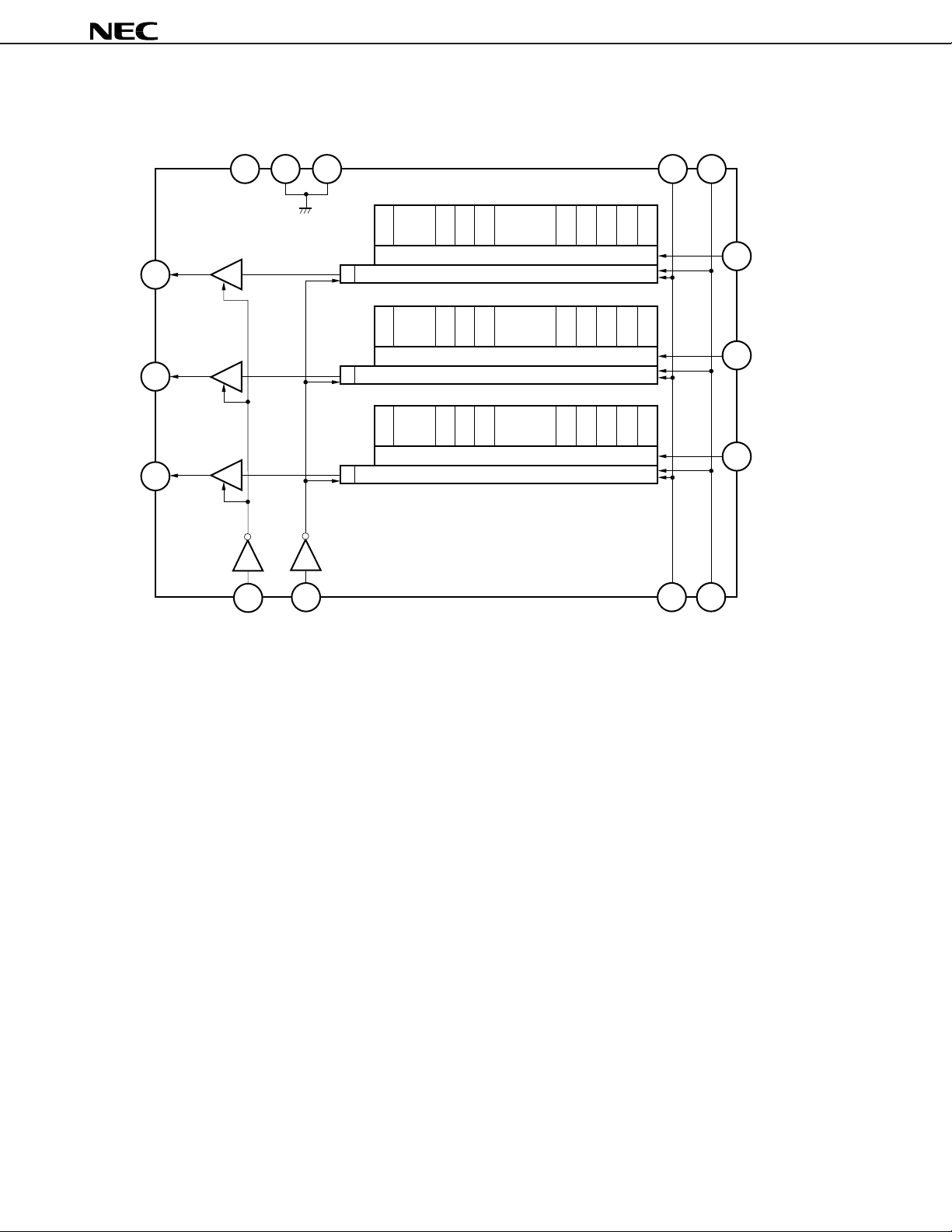
BLOCK DIAGRAM
30
GND GNDVOD
2 11
φ
2
25 24
µ
PD3798
φ
1
V
OUT1
(Blue)
V
OUT2
(Green)
VOUT3
(Red)
31
32
······
D14
······
D14
······
D14
1
3
φ
RB
φ
4
CLB
D31
CCD analog shift register
D31
CCD analog shift register
D31
CCD analog shift register
Photocell
S1
S2
(Blue)
Transfer gate
Photocell
S1
S2
(Green)
Transfer gate
Photocell
S1
S2
(Red)
Transfer gate
S5347
S5348
S5347
S5348
S5347
S5348
D32
D32
D32
D33
D33
D33
D34
D34
D34
φ
TG1
23
(Blue)
φ
TG2
22
(Green)
φ
TG3
10
(Red)
98
φ
φ
2
1
2
DATA SHEET S14314EJ1V0DS00

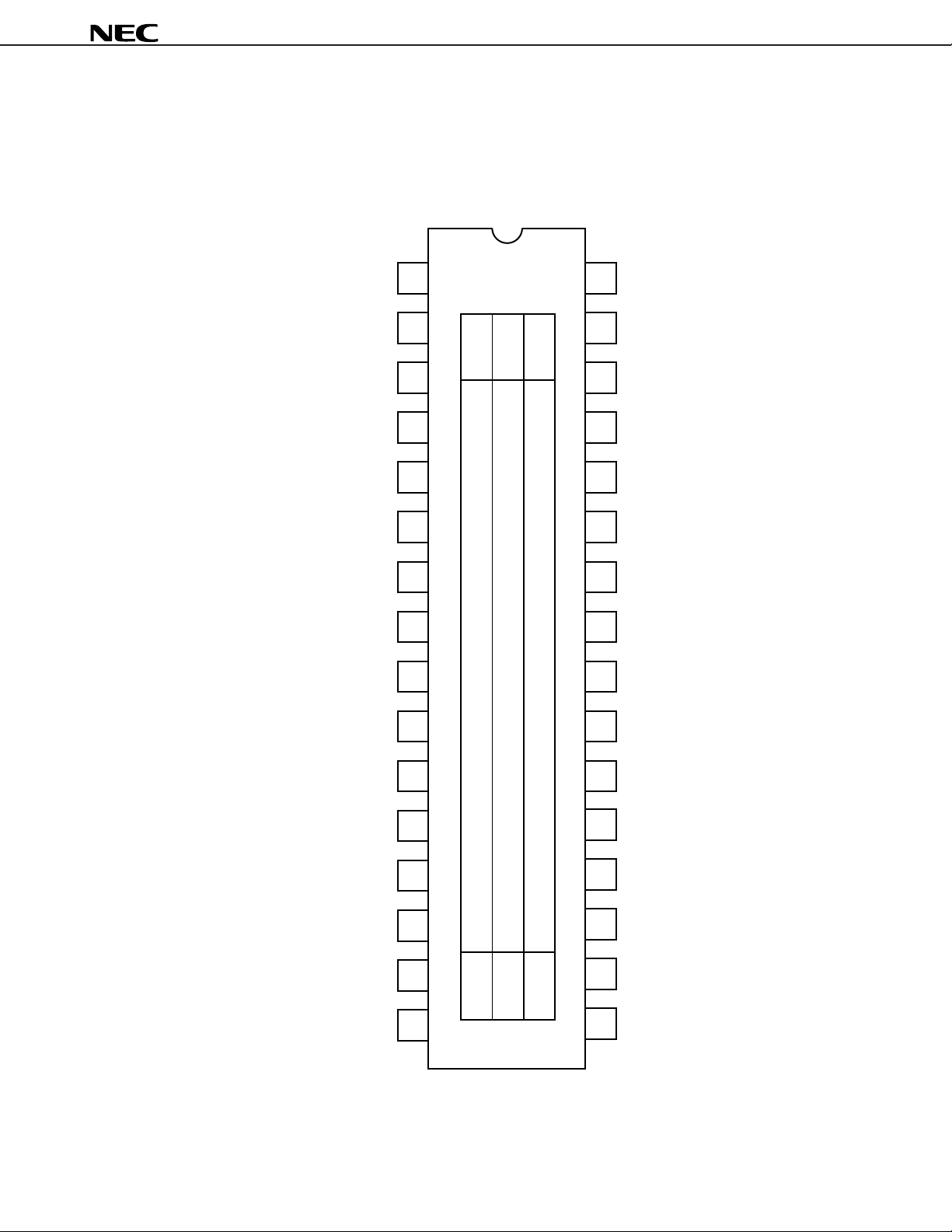
PIN CONFIGURATION (Top View)
CCD linear image sensor 32-pin plastic DIP (400 mil)
•µPD3798CY
OUT
3
Output signal 3 (Red)
V
1
32
µ
PD3798
V
OUT
2
Output signal 2 (Green)
Ground
Reset gate clock
Reset feed-through level
clamp clock
No connection
Internal connection
Internal connection
Shift register clock 2
Shift register clock 1
Transfer gate clock 3
(for Red)
Ground
GND
φ
φ
CLB
φ
TG3
GND
RB
NC
IC
IC
φ
φ
2
1
1
1
3
4
5
6
7
8
2
9
1
10
11
Red
Green
Blue
31
30
29
28
27
26
25
24
23
22
V
V
NC
NC
IC
IC
φ
φ
φ
φ
OUT
OD
2
1
TG1
TG2
1
Output signal 1 (Blue)
Output drain voltage
No connection
No connection
Internal connection
Internal connection
Shift register clock 2
Shift register clock 1
Transfer gate clock 1
(for Blue)
Transfer gate clock 2
(for Green)
12
Internal connection
Internal connection
No connection
No connection
No connection
IC
IC
NC
NC
NC
13
14
15
16
5348
5348
5348
Caution Leave pins 6, 7, 12, 13, 20, 21, 26, 27 (IC) unconnected.
DATA SHEET S14314EJ1V0DS00
IC
21
IC
20
NC
19
NC
18
17
NC No connection
Internal connection
Internal connection
No connection
No connection
3

µ
PD3798
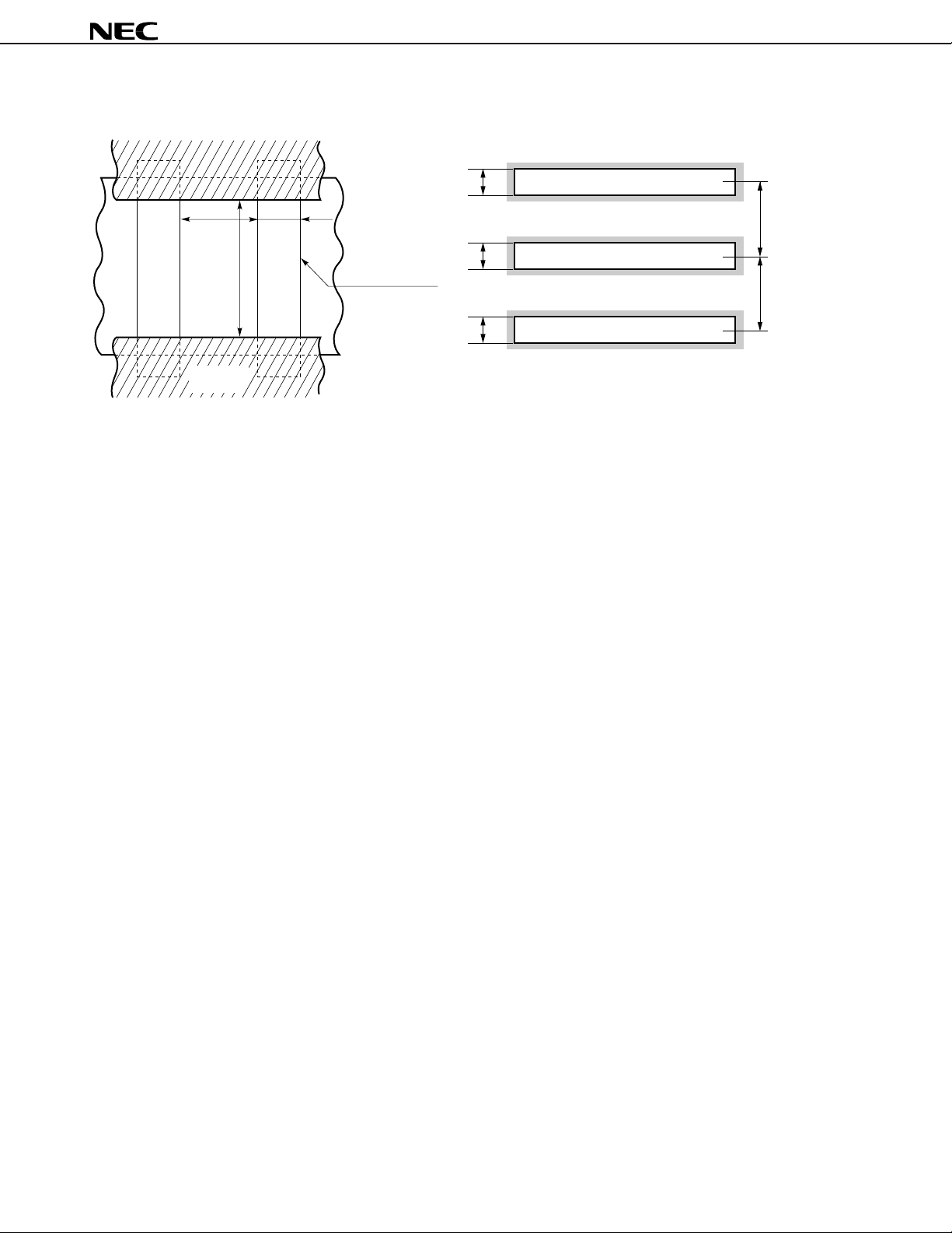
PHOTOCELL STRUCTURE DIAGRAM PHOTOCELL ARRAY STRUCTURE DIAGRAM
(Line spacing)
7 m
4 m
µ
Aluminum
shield
µ
7 m
3
m
µ
Channel stopper
µ
7 m
µ
7 m
µ
Blue photocell array
Green photocell array
Red photocell array
4 lines
(28 m)
µ
4 lines
(28 m)
µ
4
DATA SHEET S14314EJ1V0DS00

µ
PD3798
ABSOLUTE MAXIMUM RATINGS (TA = +25 °C)
Parameter Symbol Ratings Unit
Output drain voltage VOD –0.3 to +15 V
Shift register clock voltage V
Reset gate clock voltage V
Reset feed-through level clamp clock voltage V
Transfer gate clock voltage V
φ
1, Vφ2 –0.3 to +8 V
φ
RB –0.3 to +8 V
φ
CLB –0.3 to +8 V
φ
TG1
to V
φ
TG3 –0.3 to +8 V
Operating ambient temperature TA –25 to +60 °C
Storage temperature Tstg –40 to +70 °C
Caution Exposure to ABSOLUTE MAXIMUM RATINGS for extended periods may affect device reliability;
exceeding the ratings could cause permanent damage. The parameters apply independently.
RECOMMENDED OPERATING CONDITIONS (TA = +25 °C)
Parameter Symbol MIN. TYP. MAX. Unit
Output drain voltage VOD 11.4 12.0 12.6 V
Shift register clock high level V
Shift register clock low level V
Reset gate clock high level V
Reset gate clock low level V
Reset feed-through level clamp clock high level V
Reset feed-through level clamp clock low level V
Transfer gate clock high level V
Transfer gate clock low level V
Data rate f
φ
1H, Vφ2H 4.5 5.0 5.5 V
φ
1L, Vφ2L –0.3 0 +0.5 V
φ
RBH 4.5 5.0 5.5 V
φ
RBL –0.3 0 +0.5 V
φ
CLBH 4.5 5.0 5.5 V
φ
CLBL –0.3 0 +0.5 V
φ
TG1H
to V
φ
TG3H 4.5 V
φ
TG1L
to V
φ
TG3L –0.3 0 +0.5 V
φ
RB – 1.0 5.0 MHz
Note
φ
1H
Note
V
φ
1H
V
Note When Transfer gate clock high level (V
Image lag can increase.
DATA SHEET S14314EJ1V0DS00
φ
TG1H to VφTG3H) is higher than Shift register clock high level (Vφ1H),
5

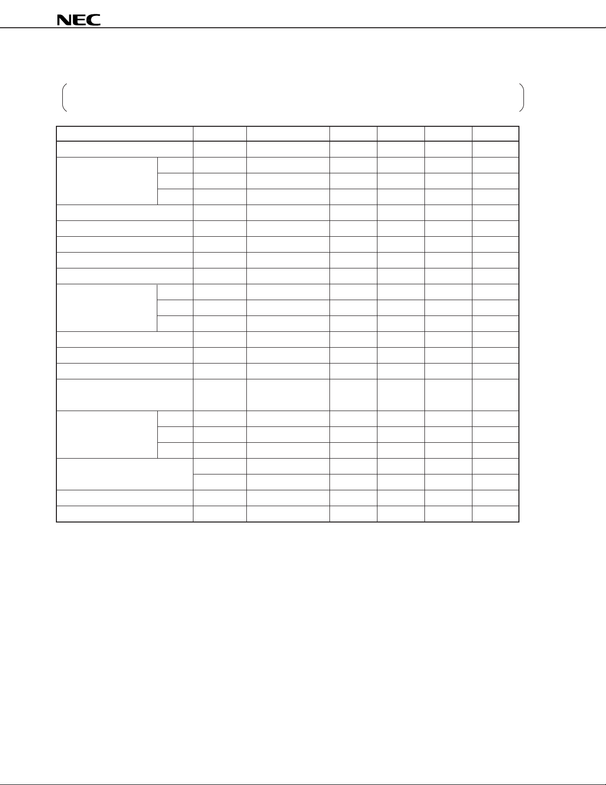
ELECTRICAL CHARACTERISTICS
µ
PD3798
TA = +25 °C, VOD = 12 V, data rate (f
φ
RB) = 1 MHz, storage time = 5.5 ms, input signal clock = 5 Vp-p
light source: 3200 K halogen lamp +C-500S (infrared cut filter, t = 1mm) + HA-50 (heat absorbing filter, t = 3 mm)
Parameter Symbol Test Conditions MIN. TYP. MAX. Unit
Saturation voltage Vsat 2.0 2.5 – V
Saturation exposure Red SER 0.223 lx•s
Green SEG 0.245 lx•s
Blue SEB 0.409 lx•s
Photo response non-uniformity PRNU VOUT = 1.0 V 6 20 %
Average dark signal ADS Light shielding 0.2 2.0 mV
Dark signal non-uniformity DSNU Light shielding 1.5 3.0 mV
Power consumption PW 360 540 mW
Output impedance ZO 0.5 1 kΩ
Response Red RR 7.8 11.2 14.6 V/lx•s
Green RG 7.1 10.2 13.3 V/lx•s
Blue RB 4.2 6.1 8.0 V/lx•s
Image lag IL VOUT = 1.0 V 1.5 7.0 %
Offset level
Output fall delay time
Total transfer efficiency TTE VOUT = 1.0 V, 92 98 %
Response peak Red 630 nm
Dynamic range DR1 Vsat /DSNU 1666 times
Reset feed-through noise
Random noise σ Light shielding – 1.0 – mV
Note1
VOS 4.0 5.5 7.0 V
Note2
Green 540 nm
Blue 460 nm
Note1
td VOUT = 1.0 V 40 ns
data rate = 5 MHz
DR2 Vsat /σ 2500 times
RFTN Light shielding –1000 –300 +500 mV
Notes 1. Refer to TIMING CHART 2.
2. When the fall time of
6
φ
1 (t1) is the TYP. value (refer to TIMING CHART 2).
DATA SHEET S14314EJ1V0DS00
 Loading...