NEC UPD3753CY Datasheet

DATA SHEET
MOS INTEGRATED CIRCUIT
µ
PD3753
2088-BIT CCD LINEAR IMAGE SENSOR WITH PERIPHERAL CIRCUIT
The µPD3753 is a 2088-bit high sensitivity CCD (Charge Coupled Device) linear image sensor which
changes optical images to electrical signal.
The µPD3753 consists of 2088-bit photocell array and a line of 2088-bit CCD charge transferred register.
It contains a reset a feed-through level clamp circuit, a pulse generator, and a voltage amplifier to provide
high sensitivity and low noise. It also supports low power consumption with single 5 V power supply. The
µ
PD3753 can be driven by power supply and three input clocks owing to the built-in reset pulse generator
and a clamp pulse generator.
FEATURES
• Valid photocell : 2088-bit
• Photocell's pitch : 14
• High response sensitivity : Providing a response equal with the existing equivalent NEC
• Low noise : Providing about two thirds register imbalance of the existing equivalent
• Peak response wavelength : 550 nm (green)
• Resolution : 8 dot/mm across the shorter side of a B4-size (257 × 364 mm) sheet
• Power supply : +5 V
• Drive clock level : CMOS output under +5 V operation
• Scanning speed : 1.0 ms/line
• Built-in circuit : Reset feed-through level clamp circuit, reset pulse generator, clamp pulse
ORDERING INFORMATION
Part Number Package Quality Grade
µ
PD3753CY CCD LINEAR IMAGE SENSOR 22 PIN PLASTIC DIP (400 mil) Standard
Please refer to "Quality grade on NEC Semiconductor Devices" (Document number IEI-1209) published by
NEC Corporation to know the specification of quality grade on the devices and its recommended applications.
µ
m
µ
product (
NEC product (µPD3743)
generator
PD3743) to the light from a daylight fluorescent lamp
Document No. IC-3429
(O. D. No. IC-9002)
Date Published August 1994 P
Printed in Japan
The information in this document is subject to change without notice.
©
1994

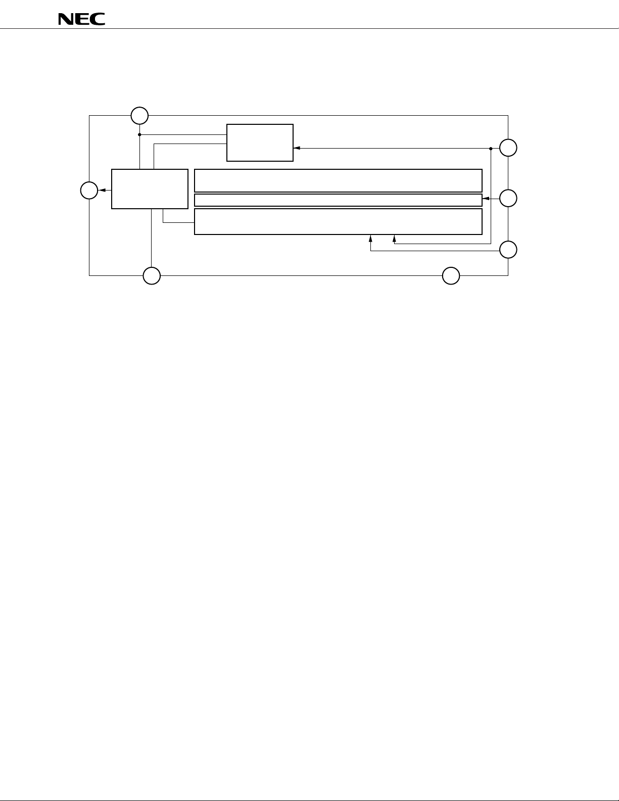
BLOCK DIAGRAM
VOD
3
Reset pulse/
clamp pulse
generator
µ
PD3753
φ
2
15
VOUT
•Voltage amplifier
•Reset feed-through
19
level clamp circuit
Optical black (OB) 18 bits, invalid 2 bits,
valid photocell 2088 bits, invalid 2 bits
CCD register
20 13
AGND DGND
14
9
φ
TG
φ
1
2

PIN CONFIGURATION (Top View)
CCD LINEAR IMAGE SENSOR 22 PIN PLASTIC DIP (400 mil)
µ
PD3753
No connection
No connection
Output unit drain voltage
No connection
No connection
No connection
No connection
No connection
Transfer gate clock
No connection
No connection
122
NC
221
NC
OD
320
V
419
NC
518
NC
617
NC
716
NC
815
NC
φ
914
TG
NC
10 13
11 12
NC NC
NC
NC
AGND
OUT
V
NC
NC
NC
φ
φ
DGND
2
1
No connection
No connection
Analog GND
Output
No connection
No connection
No connection
Shift register clock 2
Shift register clock 1
Digital GND
No connection
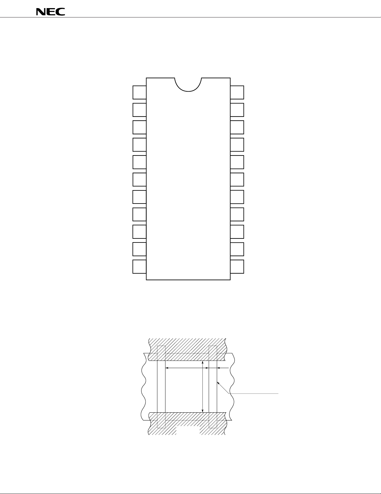
PHOTOCELL STRUCTURE DIAGRAM
12 m
µ
Aluminum
electrode
µ
14 m
2 m
µ
Channel stopper
3

ABSOLUTE MAXIMUM RATINGS (Ta = +25 °C)
Parameter Symbol Ratings Unit
Output unit drain voltage VOD –0.3 to +8 V
Shift register clock voltage V
Transfer gate signal voltage V
φ
1, φ2 –0.3 to +8 V
φ
TG –0.3 to +8 V
Operating ambient temperature Topt –25 to +60 °C
Storage temperature Tstg –40 to +70 °C
RECOMMENDED OPERATING CONDITIONS (Ta = –25 to + 60 °C)
Parameter Symbol MIN. TYP. MAX. Unit
Output unit drain voltage VOD 4.7 5.0 5.3 V
µ
PD3753
Shift register clock φ1, φ2 signal high level V
Shift register clock φ1, φ2 signal low level V
Transfer gate signal high level V
Transfer gate signal low level V
Data rate f
Caution When V
φ
TGH > Vφ1H, image lag increases.
φ
1H, φ2H 4.5 5.0 VOD + 0.2 V
φ
1L, φ2L –0.3 0 +0.5 V
φ
TGH 4.5 Vφ1H Vφ1H V
φ
TGL –0.3 0 +0.5 V
φ
R 0.2 1 2 MHz
4

µ
PD3753
ELECTRICAL CHARACTERISTICS
Ta = +25 °C, VOD = 5 V, f
light source: 3200 K halogen lamp + C500 (infrared cut filter), input clock = 5 V
Parameter Symbol Test Conditions MIN. TYP. MAX. Unit
Saturation voltage Vsat 1.0 1.2 V
Saturation exposure SE Daylight color fluorescent lamp 0.013 lx•s
Photo response non-uniformity PRNU VOUT = 500 mV ± 2 ± 8 %
Average dark signal ADS Light shielding 1.0 8.0 mV
Dark signal non-uniformity DSNU Light shielding – 8 ± 4 + 8 mV
Power consumption PW 30 50 mW
Output impedance ZO 0.5 1 kΩ
Response RF Daylight color fluorescent lamp 63 90 117 V/lx•s
Response peak wavelength 550 nm
Image lag IL VOUT = 1 V 7 14 %
φ
1 = 1 MHz, data rate = 1 MHz, storage time = 10 ms
P-P
Offset level VOS 2.5 3.0 3.5 V
C
φ
Input capacitance of shift register
clock pin
Input capacitance of transfer gate
signal pin
Output fall delay time td 130 ns
Total transfer efficiency TTE VOUT = 1 V, data rate = 2 MHz 92 %
Dynamic range DR Vsat /DSNU 375 times
Reset feed-through noise RFSN Light shielding 0 800 1500 mV
Bit noise BN Light shielding 10 mVP-P
Resolution MTF 65 %
1
C
φ
2
C
φ
TG 100 pF
Modulation transfer function at
nyquist frequency
300 pF
Remark When VOD = 4.7 V, the response typically decreases to 90 % of the value under 5 V operation.
5
 Loading...